EP3407145B1 - Fpga-based square-wave generator and square-wave generation method - Google Patents
Fpga-based square-wave generator and square-wave generation method Download PDFInfo
- Publication number
- EP3407145B1 EP3407145B1 EP16885492.5A EP16885492A EP3407145B1 EP 3407145 B1 EP3407145 B1 EP 3407145B1 EP 16885492 A EP16885492 A EP 16885492A EP 3407145 B1 EP3407145 B1 EP 3407145B1
- Authority
- EP
- European Patent Office
- Prior art keywords
- square wave
- delay
- wave signal
- clock
- waveform data
- Prior art date
- Legal status (The legal status is an assumption and is not a legal conclusion. Google has not performed a legal analysis and makes no representation as to the accuracy of the status listed.)
- Active
Links
- 238000000034 method Methods 0.000 title claims description 31
- 238000006243 chemical reaction Methods 0.000 claims description 23
- 230000003111 delayed effect Effects 0.000 claims description 16
- 230000000630 rising effect Effects 0.000 claims description 10
- 230000001934 delay Effects 0.000 claims description 3
- 238000007726 management method Methods 0.000 description 21
- 230000006870 function Effects 0.000 description 9
- 238000010586 diagram Methods 0.000 description 8
- 238000004891 communication Methods 0.000 description 7
- 238000005516 engineering process Methods 0.000 description 7
- 230000008569 process Effects 0.000 description 6
- 230000008901 benefit Effects 0.000 description 4
- 238000011161 development Methods 0.000 description 4
- 230000010354 integration Effects 0.000 description 4
- 230000005540 biological transmission Effects 0.000 description 3
- 230000008859 change Effects 0.000 description 3
- 238000013461 design Methods 0.000 description 3
- 238000005259 measurement Methods 0.000 description 3
- 238000012986 modification Methods 0.000 description 3
- 230000004048 modification Effects 0.000 description 3
- 230000001133 acceleration Effects 0.000 description 2
- 230000002093 peripheral effect Effects 0.000 description 2
- 238000011160 research Methods 0.000 description 2
- 230000007704 transition Effects 0.000 description 2
- 238000005481 NMR spectroscopy Methods 0.000 description 1
- 238000004458 analytical method Methods 0.000 description 1
- 230000005587 bubbling Effects 0.000 description 1
- 238000013500 data storage Methods 0.000 description 1
- 230000001419 dependent effect Effects 0.000 description 1
- 238000002059 diagnostic imaging Methods 0.000 description 1
- 238000000804 electron spin resonance spectroscopy Methods 0.000 description 1
- 238000002474 experimental method Methods 0.000 description 1
- 238000004949 mass spectrometry Methods 0.000 description 1
- 238000012545 processing Methods 0.000 description 1
- 230000004044 response Effects 0.000 description 1
Images
Classifications
-
- G—PHYSICS
- G06—COMPUTING; CALCULATING OR COUNTING
- G06F—ELECTRIC DIGITAL DATA PROCESSING
- G06F13/00—Interconnection of, or transfer of information or other signals between, memories, input/output devices or central processing units
- G06F13/38—Information transfer, e.g. on bus
- G06F13/382—Information transfer, e.g. on bus using universal interface adapter
- G06F13/387—Information transfer, e.g. on bus using universal interface adapter for adaptation of different data processing systems to different peripheral devices, e.g. protocol converters for incompatible systems, open system
-
- G—PHYSICS
- G04—HOROLOGY
- G04F—TIME-INTERVAL MEASURING
- G04F10/00—Apparatus for measuring unknown time intervals by electric means
-
- G—PHYSICS
- G06—COMPUTING; CALCULATING OR COUNTING
- G06F—ELECTRIC DIGITAL DATA PROCESSING
- G06F1/00—Details not covered by groups G06F3/00 - G06F13/00 and G06F21/00
- G06F1/04—Generating or distributing clock signals or signals derived directly therefrom
- G06F1/14—Time supervision arrangements, e.g. real time clock
-
- G—PHYSICS
- G06—COMPUTING; CALCULATING OR COUNTING
- G06F—ELECTRIC DIGITAL DATA PROCESSING
- G06F13/00—Interconnection of, or transfer of information or other signals between, memories, input/output devices or central processing units
- G06F13/38—Information transfer, e.g. on bus
Definitions
- the present disclosure relates to the technical field of square wave generation, and in particular, to a square wave generator and a method for generating a square wave based on a Field Programmable Gate Array (FPGA).
- FPGA Field Programmable Gate Array
- US 4 468 746 A discloses an apparatus for determining interval between two events.
- the interval between first and second events which may occur in a period less than a nanosecond interval, is determined with a square wave clock source started in response to the first event.
- the source derives a square wave having a first transition when started and equally spaced succeeding transitions spaced from each other by T/2, where T is the square wave period.
- a delay network having N taps is responsive to the square wave, whereby (N+1) square waves are derived.
- the taps are spaced from each other so the clock source square wave is delayed at tap k by kT/n, where n is a predetermined integer greater than 1 and k is selectively every integer from 1 to N.
- (N+1) memory elements respectively respond to the (N+1) square waves to generate a signal indicative of which half cycle of each of the (N+1) square wave is being derived when the second event occurs.
- the waveform generating device comprises a waveform generating management module based on a FPGA (Field Programmable Gate Array) and a peripheral circuit expansion module.
- the waveform generating management module comprises a core management unit, a data transmission control unit, a storage control unit, a system clock management unit and a data rate acceleration unit, wherein the data transmission control unit is connected to the core management unit; the storage control unit is connected to the core management unit; the system clock management unit is connected to the core management unit; and the data rate acceleration unit is used for outputting waveform data at an accelerated output rate.
- the peripheral circuit expansion module comprises a data transmission bus control unit, a storage unit, a digital-analog conversion unit and an output clock management unit. The invention is high in flexibility and can achieve a high-speed digital waveform generation and control function.
- CN 104 597 748 A discloses a FPGA (field programmable gate array) chip-based TDC (time-digital converter).
- the TDC comprises a pulse signal generator, a multi-tap signal delay chain, a trigger array, two parallel signal change edge search circuits, a rising edge 'one-hot' coding circuit, a falling edge 'one-hot' coding circuit, a calibration circuit and a conversion result output circuit, wherein the rising edge 'one-hot' coding circuit is parallel to the falling edge 'one-hot' coding circuit;
- the pulse signal generator is used for generating a negative pulse and feeding the negative pulse into the signal delay chain;
- the trigger array is used for latching states of all taps; after the taps are resorted, the states of the taps are transmitted to the signal change edge search circuits to search a rising edge and a falling edge of the negative pulse respectively, and corresponding 'one-hot' codes are generated.
- the TDC can remove 0 delay units on the delay chain to the maximum extent, reduce 'bubbling' phenomena in latch-state thermometer codes and enable performance indexes in three aspects of measurement precision, measurement dead time and resource occupancy to be reasonably balanced so as to realize a high-performance measurement system of the TDC.
- square wave generators have been widely applied in fields of electronic science and technology, communications, physics, chemistry, biology, and even medical science.
- Square waves with high-speed and high-precision can be applied to situations such as ultrasonic, radar, medical imaging, communications, and laser control, and to frontier scientific research fields such as electron paramagnetic resonance, nuclear magnetic resonance, and mass spectrometry.
- frontier scientific research fields such as electron paramagnetic resonance, nuclear magnetic resonance, and mass spectrometry.
- a resolution of the square wave may be controlled to be 2 ns by using a high-speed clock.
- a (Double Date Rate) DDR is adopted to store waveform data, and communication with a master computer for transmitting a waveform parameter is achieved via an Ethernet or a PCI bus.
- the digital logics of the FPGA reads the waveform parameters from the DDR, and outputs a waveform by using the high-speed serialization technology after completing the waveform analysis.
- a minimum limit of a width of the square wave is 12 ns according to a waveform data storage framework based on DDR3.
- DTC Digital to Time Convert, digital-to-time converter
- PLL Phase Locked Loop
- an issue for those skilled in the art to address is to provide a square wave generator which can continuously output the square wave with high precision, large dynamic range and low dead time and to provide a method for generating the square wave.
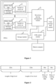
- FIG. 1 is a schematic structural diagram of a square wave generator based on an FPGA according to the present disclosure.
- the square wave generator includes a bus control module, a waveform playing management module 2, a parallel-in serial-out conversion module 3, a delay chain module 4, and a multiplex controller 5.
- the bus control module is configured to receive a playing instruction and a playing address which are sent by a master computer, and output the playing instruction and the playing address.
- the bus control module is a USB bus control module 1.
- USB bus control module 1 is arranged inside the FPGA, and the USB bus control module 1, which is based on a USB bus, is configured to establish communications between the FPGA and the master computer via the USB bus.
- the communications includes a downloading and updating of a control command and raw waveform data.
- bus control module herein may also be a bus control module of another type, which is not limited by the present disclosure.
- the waveform playing management module 2 is configured to receive the playing instruction and the playing address, read the raw waveform data from a storage module 6 according to the playing instruction and the playing address, decode the raw waveform data to obtain a waveform data, generate delay data according to the waveform data, and output the waveform data and the delay data.
- the storage module 6 is specifically configured to receive, via the bus control module, a storage command, a storage address, and the raw waveform data which are sent by the master computer, decode the storage address according to the storage command, and store the raw waveform data according to a decoded storage address.
- the master computer is configured to send the storage command, the storage address, and the raw waveform data to the USB bus control module 1 via the USB bus at first, and then the USB bus control module 1 sends the storage command, the storage address, and the raw waveform data to the storage module 6.
- the storage module 6 decodes the storage address, and then stores the raw waveform data into the storage module 6 according to the decoded storage address.
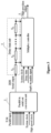
- each square wave signal in the raw waveform data occupies 80 bits in the storage module 6, where a first group of 32 bits in the 80 bits contains information of holding a high level in the each square wave signal, a second group of 32 bits in the 80 bits contains information of holding a low level in the each square wave signal, a third group of 8 bits in the 80 bits contains information of a delay time between a rising edge of the each square wave signal and a clock edge of the high-speed clock, and a fourth group of 8 bits in the 80 bits contains information of a delay time between a falling edge of the each square wave signal and another clock edge of the high-speed clock.
- Figure 2 is a schematic diagram of a storage structure of a square wave signal according to the present disclosure.
- the raw waveform data of the square wave with high precision is stored in the storage module 6 inside the FPGA.
- Data of each square wave signal in the raw waveform data is stored in the storage module 6 based on the structure shown in Figure 2 .
- the effective information is: a time duration for holding the high level (a logic "1"), a time duration for holding the low level (a logic "0"), and delay times for the rising edge and the falling edge of the square wave in relative to the clock edge of the high-speed clock.
- the each square wave signal occupies a total of 80 bits of data. In the 80 bits, a first group of 32 bits contains information on holding the high level (i.e.
- a second group of 32 bits contains information on holding the low level (i.e. the logic "0") in the each square wave signal, and a period T of the high-speed clock is represented by a lowest bit of these two groups of 32 bits.
- the information on the delay time between the rising edge of the each square wave signal and the clock edge of the high-speed clock i.e., a delay of a leading edge as shown in Figure 2 occupies the third group of 8 bits
- the information on the delay time between the falling edge of the each square wave signal and another clock edge of the high-speed clock i.e., a delay of a trailing edge as shown in Figure 2 occupies the fourth group of 8 bits
- a delay time of a single delay unit in the delay chain unit 4 is represented by a lowest bit of these two groups of 8 bits.
- a total delay time of the delay chain unit 4 is not shorter than the period of the high-speed clock.
- t indicating an arrival time of signal edge of the square wave signal is determined by two factors.
- One factor is time data of parallel input with relatively low precision, which is set as n 1 * T 2 , where n 1 represents total time duration of square wave signals before the current square wave signal arrives, and is determined by the sum of a high-level time and a low-level time.
- a relative delay and a pulse width of the square wave can be precisely adjusted.
- a minimum adjustable precision of the square wave is t 0 , in a case that t 0 is much shorter than T .
- the total time duration of the delay chain should cover at least the period T of the high-speed clock.
- a time interpolation for the high-speed clock is realized by using the parallel-in serial-out conversion unit 3 in the FPGA in conjunction with the delay chain unit 4, so that a time resolution that is equal to the delay time of the single delay unit in the delay chain unit 4 is obtained.
- T 2 n + 1 2 * t 0 , where n represents a positive integer.
- the two value are further analyzed and processed in the FPGA in real time, and then sent to a square wave outputting module (including the parallel-in serial-out conversion unit 3, the delay chain unit 4, and the multiplex controlling unit 5) for output.
- a square wave outputting module including the parallel-in serial-out conversion unit 3, the delay chain unit 4, and the multiplex controlling unit 5 for output.
- a precision 1/2* t 0 for adjusting the signal edge of the square wave signal is realized.
- the time precision of the square wave signal can be doubled by using time interpolation alternately. Meanwhile, a characteristic of an outputting square wave at a high speed is also ensured, without influencing other basic parameters of the square wave generator such as a dead time and a dynamic range.
- n is 12 and t 0 is 50 ps.
- T is 1.25 ns and the time resolution is t 0 2 , i.e. 25 ps. Hence, the precision is high.
- n and t 0 are determined according to a practical implementation, and different values may be set for different square wave generators.
- the parallel-in serial-out conversion unit 3 is configured to receive the waveform data inputted in parallel, and output the waveform data in serial to obtain a square wave signal.
- the parallel-in serial-out conversion unit 3 is configured to receive, according to a system clock, the waveform data inputted in parallel, and output, according to the high-speed clock, the square wave signal in serial in a DDR manner, where a frequency of the high-speed clock is 4 times as large as a frequency of the system clock.
- the delay chain unit 4 is configured to delay the square wave signal
- the delay chain unit 4 is capable to achieve high-precision delay on the square wave signal and obtain an output of the square wave signal with high time resolution.
- the multiplex controller 5 is configured to receive the delay data, determine an output node of the square wave signal on the delay chain unit 4 according to the delay data, obtain from the output node a delayed square wave signal corresponding to the output node, and output the delayed square wave signal.
- Figure 3 is a schematic structural diagram of a square wave outputting module according to the present disclosure.
- the square wave outputting module herein includes the parallel-in serial-out conversion unit 3, the delay chain unit 4, and the multiplex controller 5. Moreover, multiple square wave outputting modules may be included in the square wave generator. A specific quantity of the multiple square wave outputting modules is not limited herein according to the present disclosure.
- the square wave outputting module is an important part of the present disclosure.
- the square wave outputting module is configured to perform time interpolation on the high-speed clock to output the square wave signal having higher time resolution and no dead time.
- a diagram of an internal structural diagram of the square wave outputting module is shown in Figure 3 .
- An operating clock of the parallel-in serial-out conversion unit 3 and the multiplex controller 5 is a system clock.
- the high-speed clock is an output reference clock for the high-speed square wave, and the frequency of the high-speed clock is 4 times as large as the frequency of the system clock.
- the parallel-in serial-out conversion unit 3 outputs the square wave signal at both the rising edge and the falling edge of the high-speed clock, namely, outputs at a double-rate output (Double Data Rate, DDR).
- DDR Double Data Rate
- 8-bit parallel waveform data is inputted into the parallel-in serial-out conversion unit 3 according to the system clock.
- the parallel-in serial-out conversion unit 3 outputs, according to the high-speed clock a square wave signal with 8 bits per period of the system clock in the DDR manner.
- the square wave signal outputted in serial by the parallel conversion unit 3 is sent to the delay chain unit 4.
- the multiplex controller 5 determines, according to the inputted delay data in real time, a sequence number of the output node of the delay chain unit 4, obtains a delayed square wave signal corresponding to the output node from the output node, and outputs the delayed square wave signal. Different output nodes in the delay chain correspond to different delays.
- the time precision of the square wave is equal to the time delay t 0 of the single delay unit in the delay chain unit 4.
- a square wave with high precision can be generated. Meanwhile, the capability to output a sequence of square wave at a high speed is ensured, where the square wave has no dead time and a dynamic range from nanoseconds to seconds.
- the square wave generator further comprises a clock management module 7.
- the clock management module 7 is configured to receive a reference clock inputted externally, and generate, according to the reference clock, an operating clock for the bus control module, the waveform playing management module 2, the parallel-in serial-out conversion unit 3, and the multiplex controller 5, where the operating clock is the system clock.
- the clock management module 7 is further configured to generate, according to the reference clock, the high-speed clock for the parallel-in serial-out conversion unit 3.
- the square wave generator provided by the present disclosure is based on the FPGA.
- the FPGA selected in the present disclosure is a Virtex-7 FPGA of an SRAM type.
- the Virtex-7 FPGA is based on a look-up table having six inputs. A 28 nm CMOS process is applied in this FPGA so that more than 10 million gate circuits and thousands of customizable I/O can be integrated into a single chip.
- the Virtex-7 FPGA has a highest integration and a good performance.
- the storage module 6, which is generated by calling internal resources of the FPGA, is configured to store the waveform data for the square wave generator having a high-speed and high-precision based on the FPGA.
- the USB bus control module 1 is arranged inside the FPGA so as to establish communications between the FPGA and the master computer via the USB bus, where the communications includes a downloading and updating of a control command and waveform data.
- Data decoding, control and state management is performed in a playing process of the square wave waveform by the waveform playing management module 2 using logic resources of the FPGA.
- a function to output the high-precision square wave is further realized in conjunction with the high-speed parallel-in serial-out conversion unit 3 and the delay chain unit 4 in the FPGA.
- the clock management module 7 is designed by using clock management resources inside the FPGA.
- the operating clock for the USB bus control module 1, the memory module 6, the waveform playing management module 2, and the high-speed square wave outputting module (including the parallel-in serial-out conversion unit 3, the delay chain unit 4, and the multiplex controller 5) is generated based on the reference clock which is externally inputted.
- the square wave generator based on the Virtex-7 FPGA is of low cost.
- a multi-channel superposed waveform generator is achieved by using the Virtex-7 FPGA as a key processing chip.
- a cost of a single FPGA chip is about 20,000-30,000 Chinese yuan, and a total cost of a single device is about 40,000 Chinese yuan, where this price is equal to the price of a Pulseblaster with a time resolution of mere 1-2 ns.
- modifications may only be made to logic configurations inside the FPGA, rather than hardware configurations, which can greatly reduce a cost of secondary development.
- a square wave generating function having 10 channels with high-speed and high-resolution is achieved in a Virtex-7 FPGA XC7V485T-2 of a SRAM type.
- the time resolution of the square wave obtained by the time interpolation based on the delay chain can be approximate 50 ps, with no dead time in outputting the square wave and with a dynamic range from 5 ns to seconds. Time precision can be improved to 25 ps by using the time interpolation alternately further.
- the square wave generator based on the Virtex-7 FPGA is of high performance and high level of integration.
- the Virtex-7 FPGA with characteristics of high performance and a high speed are used as a basis of the design.
- a generating and outputting structure of a digital signal are optimized.
- Limitations of the conventional technology are broken, and a performance comparable to a customized ASIC can be obtained.
- Multiple square wave generating channels can be integrated into a single FPGA, which greatly improves an integration level of a system.
- a square wave generator with high speed, high precision, low cost, strong design flexibility and high integration level is realized based on the Virtex-7 FPGA, which can be applied to many implementations.
- the Virtex-7 FPGA By using the high performance and re-programmability of the Virtex-7 FPGA, various functions in various implementations can be realized according to this disclosure.
- the function to generate a high-performance square wave is improved while ensuring flexibility thereof.
- the square wave generator based on the FPGA has high precision and no dead time.
- the time interpolation is performed on the high-speed clock by using the delay chain method, which improves the time resolution of the square wave signal while retaining characteristics of continuously outputting the high-precision square wave with a high speed and without the dead time.
- Using the time interpolation alternately can double the precision of the square wave generator without influencing performance indexes.
- the square wave generator based on the FPGA has a large dynamic range.
- the level holding time of the outputted square wave signal has a very large dynamic range, so that the square wave generator can be applied to various application scenes.
- the square wave generator based on the FPGA is of flexibility in implementation. Flexibility is a biggest advantage for a superposed waveform generator based on the FPGA with a high speed and a high resolution. A similar high-performance waveform generator based on a customized ASIC chip generally has limited functions due to a fixed function of the ASIC. It is difficult to adapt to an application scene which requires high flexibility.
- the square wave generator based on the FPGA greatly utilizes a reprogrammable characteristic of the FPGA. Different requirements can be met by a few modifications to an FPGA code, which does not require any modification on hardware. Development based on the FPGA also simplifies a developing process and difficulties thereof. In addition, the present disclosure is applicable to most application scenes which require the square wave signal due to the characteristics of high precision, no dead time and large dynamic range, and thereby having a good flexibility in application.
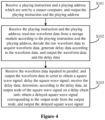
- FIG. 4 is a flowchart of a method for generating a square wave based on an FPGA according to the present disclosure. The method includes steps S101 to S103.
- step S101 a playing instruction and a playing address which are sent by a master computer are received, and the playing instruction and the playing address are outputted.
- step S102 the playing instruction and the playing address are received, raw waveform data is read from an storage module according to the playing instruction and the playing address, the raw waveform data is decoded to obtain waveform data, delay data is generated according to the waveform data, and the waveform data and the delay data are outputted.
- step S103 the waveform data inputted in parallel is received, the waveform data is outputted in serial to obtain a square wave signal, the square wave signal is delayed, the delay data is received, an output node of the square wave signal on a delay chain unit is determined according to the delay data, a delayed square wave signal corresponding to the output node is obtained from the output node, and the delayed square wave signal is outputted.
- a detailed description of the method for generating the square wave based on the FPGA may be referred to the description of the square wave generator, and is not further described herein.
- the method for generating the square wave based on the FPGA includes receiving the delay data, determining, according to the delay data, the output node of the square wave signal on the delay chain unit, obtaining the delayed square wave signal corresponding to the output node from the output node, and outputting the delayed square wave signal. Therefore, the precision of the square wave finally outputted by the square wave generator is a delay time of one single delay unit in the delay chain unit.
- the delay time of the single delay unit in the delay chain unit is as short as picoseconds, so that the square wave signal can be continuously outputted with high precision and no dead time.
- a process, a method, an article or a device including a combination of elements include the disclosed combination of elements, and may further include other elements that are not enumerated, or further include inherent elements of the process, the method, the article or the device. Unless specifically limited, the statement “including/comprising" does not exclude a case that other similar elements may exist in the process, the method, the article or the device other than the combination of elements.
Description
- The present disclosure relates to the technical field of square wave generation, and in particular, to a square wave generator and a method for generating a square wave based on a Field Programmable Gate Array (FPGA).
-
US 4 468 746 A discloses an apparatus for determining interval between two events. The interval between first and second events, which may occur in a period less than a nanosecond interval, is determined with a square wave clock source started in response to the first event. The source derives a square wave having a first transition when started and equally spaced succeeding transitions spaced from each other by T/2, where T is the square wave period. A delay network having N taps is responsive to the square wave, whereby (N+1) square waves are derived. The taps are spaced from each other so the clock source square wave is delayed at tap k by kT/n, where n is a predetermined integer greater than 1 and k is selectively every integer from 1 to N. (N+1) memory elements respectively respond to the (N+1) square waves to generate a signal indicative of which half cycle of each of the (N+1) square wave is being derived when the second event occurs. -
CN 105 162 437 A discloses a waveform generating device and method. The waveform generating device comprises a waveform generating management module based on a FPGA (Field Programmable Gate Array) and a peripheral circuit expansion module. The waveform generating management module comprises a core management unit, a data transmission control unit, a storage control unit, a system clock management unit and a data rate acceleration unit, wherein the data transmission control unit is connected to the core management unit; the storage control unit is connected to the core management unit; the system clock management unit is connected to the core management unit; and the data rate acceleration unit is used for outputting waveform data at an accelerated output rate. The peripheral circuit expansion module comprises a data transmission bus control unit, a storage unit, a digital-analog conversion unit and an output clock management unit. The invention is high in flexibility and can achieve a high-speed digital waveform generation and control function. -
CN 104 597 748 A discloses a FPGA (field programmable gate array) chip-based TDC (time-digital converter). The TDC comprises a pulse signal generator, a multi-tap signal delay chain, a trigger array, two parallel signal change edge search circuits, a rising edge 'one-hot' coding circuit, a falling edge 'one-hot' coding circuit, a calibration circuit and a conversion result output circuit, wherein the rising edge 'one-hot' coding circuit is parallel to the falling edge 'one-hot' coding circuit; the pulse signal generator is used for generating a negative pulse and feeding the negative pulse into the signal delay chain; the trigger array is used for latching states of all taps; after the taps are resorted, the states of the taps are transmitted to the signal change edge search circuits to search a rising edge and a falling edge of the negative pulse respectively, and corresponding 'one-hot' codes are generated. The TDC can remove 0 delay units on the delay chain to the maximum extent, reduce 'bubbling' phenomena in latch-state thermometer codes and enable performance indexes in three aspects of measurement precision, measurement dead time and resource occupancy to be reasonably balanced so as to realize a high-performance measurement system of the TDC. - With rapid development of electronic science and technology and related research fields in recent years, square wave generators have been widely applied in fields of electronic science and technology, communications, physics, chemistry, biology, and even medical science. Square waves with high-speed and high-precision can be applied to situations such as ultrasonic, radar, medical imaging, communications, and laser control, and to frontier scientific research fields such as electron paramagnetic resonance, nuclear magnetic resonance, and mass spectrometry. With rapid development of modern science and technology and experimental methods, there are new requirements on square waves generating function with high-speed and high-precision.
- In conventional technology, two common solutions are applied to generate the square waves with high-speed and high-precision. One solution is combining an FPGA and high-speed serialization technology, and a resolution of the square wave may be controlled to be 2 ns by using a high-speed clock. Generally, a (Double Date Rate) DDR is adopted to store waveform data, and communication with a master computer for transmitting a waveform parameter is achieved via an Ethernet or a PCI bus. The digital logics of the FPGA reads the waveform parameters from the DDR, and outputs a waveform by using the high-speed serialization technology after completing the waveform analysis. According to the above solution, square waves generating function with a high speed can be achieved, but the square wave only has a precision with an order of magnitude of nanosecond (ns), and thus failing to meet a requirement of high precision. Meanwhile, a minimum limit of a width of the square wave is 12 ns according to a waveform data storage framework based on DDR3. Another solution is using a DTC (Digital to Time Convert, digital-to-time converter) based on a vernier caliper method or a high-performance delay PLL (Phase Locked Loop), with which a time precision of picosecond or even sub-picosecond can be achieved. However, although square wave pulses with high precision can be outputted, there are some limitations for the high-precision DTC based on the vernier caliper method or based on the PLL. For example, a maximum width of an outputted pulse is limited, and a dead time of the output pulse is long, where the dead time can even reach microseconds.
- Therefore, an issue for those skilled in the art to address is to provide a square wave generator which can continuously output the square wave with high precision, large dynamic range and low dead time and to provide a method for generating the square wave.
- An objective of the present disclosure is to provide a square wave generator based on an FPGA, based on which a square wave signal having high precision and no dead time can be continuously outputted. Another objective of the present disclosure is to provide a method for generating a square wave based on an FPGA.
- To address the above technical issues, the invention is set out in the appended set of claims. According to the present invention there is provided a FPGA based square wave generator and a method for generating a square wave based on a FPGA in accordance with claims 1 and 10. Preferred embodiments are defined in dependent claims 2-9.
- For a clearer illustration of the technical solutions according to embodiments of the present disclosure, drawings used in the description of the embodiments are introduced briefly hereinafter. Apparently, the drawings described hereinafter merely illustrate some embodiments of the present disclosure, and other drawings may be obtained by those skilled in the art based on the provided drawings without creative efforts.
-
Figure 1 is a schematic structural diagram of a square wave generator based on an FPGA according to the present disclosure; -
Figure 2 is a schematic diagram of a storage structure of a square wave signal according to the present disclosure; -
Figure 3 is a schematic structural diagram of a square wave outputting module according to the present disclosure; and -
Figure 4 is a flowchart of a method for generating a square wave based on an FPGA according to the present disclosure. - An objective of the present disclosure is to provide a square wave generator based on an FPGA, which can continuously output a square wave signal with high precision and without a dead time. Another objective of the present disclosure is to provide a method for generating a square wave based on an FPGA.
- To make the objective, technical solutions and advantages of the present application clearer, the technical solutions according to the embodiments of the present application will be described clearly hereinafter in conjunction with the drawings for the embodiments of the present application. Apparently, only some embodiments rather than all embodiments, are described hereinafter. Any other embodiments obtained by those skilled in the art based on the embodiments in the present disclosure without any creative efforts fall within the protection scope of the present disclosure.
- Reference is made to
Figure 1 , which is a schematic structural diagram of a square wave generator based on an FPGA according to the present disclosure. The square wave generator includes a bus control module, a waveform playing management module 2, a parallel-in serial-out conversion module 3, adelay chain module 4, and amultiplex controller 5. - The bus control module is configured to receive a playing instruction and a playing address which are sent by a master computer, and output the playing instruction and the playing address.
- Preferably, the bus control module is a USB bus control module 1.
- It should be noted that the USB bus control module 1 is arranged inside the FPGA, and the USB bus control module 1, which is based on a USB bus, is configured to establish communications between the FPGA and the master computer via the USB bus. The communications includes a downloading and updating of a control command and raw waveform data.
- It is understood that the bus control module herein may also be a bus control module of another type, which is not limited by the present disclosure. The bus control modules of other types, which are capable to achieve the objective of the present disclosure, fall within the protection scope of the present disclosure.
- The waveform playing management module 2 is configured to receive the playing instruction and the playing address, read the raw waveform data from a
storage module 6 according to the playing instruction and the playing address, decode the raw waveform data to obtain a waveform data, generate delay data according to the waveform data, and output the waveform data and the delay data. - Further, the
storage module 6 is specifically configured to receive, via the bus control module, a storage command, a storage address, and the raw waveform data which are sent by the master computer, decode the storage address according to the storage command, and store the raw waveform data according to a decoded storage address. - It should be understood that, the master computer is configured to send the storage command, the storage address, and the raw waveform data to the USB bus control module 1 via the USB bus at first, and then the USB bus control module 1 sends the storage command, the storage address, and the raw waveform data to the
storage module 6. Thestorage module 6 decodes the storage address, and then stores the raw waveform data into thestorage module 6 according to the decoded storage address. - Preferably, each square wave signal in the raw waveform data occupies 80 bits in the
storage module 6, where a first group of 32 bits in the 80 bits contains information of holding a high level in the each square wave signal, a second group of 32 bits in the 80 bits contains information of holding a low level in the each square wave signal, a third group of 8 bits in the 80 bits contains information of a delay time between a rising edge of the each square wave signal and a clock edge of the high-speed clock, and a fourth group of 8 bits in the 80 bits contains information of a delay time between a falling edge of the each square wave signal and another clock edge of the high-speed clock. - Specifically, reference is made to
Figure 2 , which is a schematic diagram of a storage structure of a square wave signal according to the present disclosure. - The raw waveform data of the square wave with high precision is stored in the
storage module 6 inside the FPGA. Data of each square wave signal in the raw waveform data is stored in thestorage module 6 based on the structure shown inFigure 2 . For the raw waveform data with high precision of the square wave generator, the effective information is: a time duration for holding the high level (a logic "1"), a time duration for holding the low level (a logic "0"), and delay times for the rising edge and the falling edge of the square wave in relative to the clock edge of the high-speed clock. The each square wave signal occupies a total of 80 bits of data. In the 80 bits, a first group of 32 bits contains information on holding the high level (i.e. the logic "1") in the each square wave signal, a second group of 32 bits contains information on holding the low level (i.e. the logic "0") in the each square wave signal, and a period T of the high-speed clock is represented by a lowest bit of these two groups of 32 bits. The information on the delay time between the rising edge of the each square wave signal and the clock edge of the high-speed clock, i.e., a delay of a leading edge as shown inFigure 2 occupies the third group of 8 bits, and the information on the delay time between the falling edge of the each square wave signal and another clock edge of the high-speed clock, i.e., a delay of a trailing edge as shown inFigure 2 occupies the fourth group of 8 bits, and a delay time of a single delay unit in thedelay chain unit 4 is represented by a lowest bit of these two groups of 8 bits. - Preferably, the delay data includes a relationship t indicating an arrival time of signal edge of the square wave signal, where:

- n 1 represents a total time duration of square wave signals before a current square wave pulse signal arrives.
- T represents the period of the high-speed clock.
- n 2 represents a sequence number of the output node for outputting a signal in the
delay chain unit 4. - t 0 represents the delay time of the single delay unit in the
delay chain unit 4. - A total delay time of the
delay chain unit 4 is not shorter than the period of the high-speed clock. - It can be understood that the relationship t indicating an arrival time of signal edge of the square wave signal is determined by two factors. One factor is time data of parallel input with relatively low precision, which is set as


- Therefore, a time interpolation for the high-speed clock is realized by using the parallel-in serial-
out conversion unit 3 in the FPGA in conjunction with thedelay chain unit 4, so that a time resolution that is equal to the delay time of the single delay unit in thedelay chain unit 4 is obtained. - Further,

- The period T of the high-speed clock inputted into the parallel-in serial-
out conversion unit 3 is set to satisfy the equation
delay chain unit 4. For the arrival time of the signal edge of the square wave signal

out conversion unit 3, thedelay chain unit 4, and the multiplex controlling unit 5) for output. Thereby, a precision 1/2* t 0 for adjusting the signal edge of the square wave signal is realized. Namely, the time precision of the square wave signal can be doubled by using time interpolation alternately. Meanwhile, a characteristic of an outputting square wave at a high speed is also ensured, without influencing other basic parameters of the square wave generator such as a dead time and a dynamic range. - Preferably, n is 12 and t 0 is 50 ps.
- It should be understood that, in a case that n is 12 and t 0 is 50 ps, T is 1.25 ns and the time resolution is

- It should be understood that n and t 0 are determined according to a practical implementation, and different values may be set for different square wave generators.
- The parallel-in serial-
out conversion unit 3 is configured to receive the waveform data inputted in parallel, and output the waveform data in serial to obtain a square wave signal. - Preferably, the parallel-in serial-
out conversion unit 3 is configured to receive, according to a system clock, the waveform data inputted in parallel, and output, according to the high-speed clock, the square wave signal in serial in a DDR manner, where a frequency of the high-speed clock is 4 times as large as a frequency of the system clock. - The
delay chain unit 4 is configured to delay the square wave signal; - It should be understood that the
delay chain unit 4 is capable to achieve high-precision delay on the square wave signal and obtain an output of the square wave signal with high time resolution. - The
multiplex controller 5 is configured to receive the delay data, determine an output node of the square wave signal on thedelay chain unit 4 according to the delay data, obtain from the output node a delayed square wave signal corresponding to the output node, and output the delayed square wave signal. - Specifically, reference is made to
Figure 3 , which is a schematic structural diagram of a square wave outputting module according to the present disclosure. - It can be understood that the square wave outputting module herein includes the parallel-in serial-
out conversion unit 3, thedelay chain unit 4, and themultiplex controller 5. Moreover, multiple square wave outputting modules may be included in the square wave generator. A specific quantity of the multiple square wave outputting modules is not limited herein according to the present disclosure. - The square wave outputting module is an important part of the present disclosure. The square wave outputting module is configured to perform time interpolation on the high-speed clock to output the square wave signal having higher time resolution and no dead time. A diagram of an internal structural diagram of the square wave outputting module is shown in
Figure 3 . An operating clock of the parallel-in serial-out conversion unit 3 and themultiplex controller 5 is a system clock. The high-speed clock is an output reference clock for the high-speed square wave, and the frequency of the high-speed clock is 4 times as large as the frequency of the system clock. The parallel-in serial-out conversion unit 3 outputs the square wave signal at both the rising edge and the falling edge of the high-speed clock, namely, outputs at a double-rate output (Double Data Rate, DDR). 8-bit parallel waveform data is inputted into the parallel-in serial-out conversion unit 3 according to the system clock. The parallel-in serial-out conversion unit 3 outputs, according to the high-speed clock a square wave signal with 8 bits per period of the system clock in the DDR manner. The square wave signal outputted in serial by theparallel conversion unit 3 is sent to thedelay chain unit 4. Themultiplex controller 5 determines, according to the inputted delay data in real time, a sequence number of the output node of thedelay chain unit 4, obtains a delayed square wave signal corresponding to the output node from the output node, and outputs the delayed square wave signal. Different output nodes in the delay chain correspond to different delays. By the time interpolation using a delay time chain method, the time precision of the square wave is equal to the time delay t 0 of the single delay unit in thedelay chain unit 4. In this embodiment, a square wave with high precision can be generated. Meanwhile, the capability to output a sequence of square wave at a high speed is ensured, where the square wave has no dead time and a dynamic range from nanoseconds to seconds. - Preferably, the square wave generator further comprises a clock management module 7.
- The clock management module 7 is configured to receive a reference clock inputted externally, and generate, according to the reference clock, an operating clock for the bus control module, the waveform playing management module 2, the parallel-in serial-
out conversion unit 3, and themultiplex controller 5, where the operating clock is the system clock. The clock management module 7 is further configured to generate, according to the reference clock, the high-speed clock for the parallel-in serial-out conversion unit 3. - In addition, it should be noted that the square wave generator provided by the present disclosure is based on the FPGA. The FPGA selected in the present disclosure is a Virtex-7 FPGA of an SRAM type. The Virtex-7 FPGA is based on a look-up table having six inputs. A 28 nm CMOS process is applied in this FPGA so that more than 10 million gate circuits and thousands of customizable I/O can be integrated into a single chip. The Virtex-7 FPGA has a highest integration and a good performance.
- In the present disclosure, the
storage module 6, which is generated by calling internal resources of the FPGA, is configured to store the waveform data for the square wave generator having a high-speed and high-precision based on the FPGA. The USB bus control module 1 is arranged inside the FPGA so as to establish communications between the FPGA and the master computer via the USB bus, where the communications includes a downloading and updating of a control command and waveform data. Data decoding, control and state management is performed in a playing process of the square wave waveform by the waveform playing management module 2 using logic resources of the FPGA. A function to output the high-precision square wave is further realized in conjunction with the high-speed parallel-in serial-out conversion unit 3 and thedelay chain unit 4 in the FPGA. The clock management module 7 is designed by using clock management resources inside the FPGA. The operating clock for the USB bus control module 1, thememory module 6, the waveform playing management module 2, and the high-speed square wave outputting module (including the parallel-in serial-out conversion unit 3, thedelay chain unit 4, and the multiplex controller 5) is generated based on the reference clock which is externally inputted. - It should be understood that the square wave generator based on the Virtex-7 FPGA has the following advantages.
- The square wave generator based on the Virtex-7 FPGA is of low cost. A multi-channel superposed waveform generator is achieved by using the Virtex-7 FPGA as a key processing chip. A cost of a single FPGA chip is about 20,000-30,000 Chinese yuan, and a total cost of a single device is about 40,000 Chinese yuan, where this price is equal to the price of a Pulseblaster with a time resolution of mere 1-2 ns. For different implementations, modifications may only be made to logic configurations inside the FPGA, rather than hardware configurations, which can greatly reduce a cost of secondary development.
- With the principle of the present disclosure, a square wave generating function having 10 channels with high-speed and high-resolution is achieved in a Virtex-7 FPGA XC7V485T-2 of a SRAM type. The time resolution of the square wave obtained by the time interpolation based on the delay chain can be approximate 50 ps, with no dead time in outputting the square wave and with a dynamic range from 5 ns to seconds. Time precision can be improved to 25 ps by using the time interpolation alternately further.
- The square wave generator based on the Virtex-7 FPGA is of high performance and high level of integration. According to the present disclosure, the Virtex-7 FPGA with characteristics of high performance and a high speed are used as a basis of the design. A generating and outputting structure of a digital signal are optimized. Limitations of the conventional technology are broken, and a performance comparable to a customized ASIC can be obtained. Multiple square wave generating channels can be integrated into a single FPGA, which greatly improves an integration level of a system.
- According to present disclosure, a square wave generator with high speed, high precision, low cost, strong design flexibility and high integration level is realized based on the Virtex-7 FPGA, which can be applied to many implementations. By using the high performance and re-programmability of the Virtex-7 FPGA, various functions in various implementations can be realized according to this disclosure. The function to generate a high-performance square wave is improved while ensuring flexibility thereof.
- The advantages of the square wave generator based on the FPGA according to the present disclosure are described hereinafter.
- The square wave generator based on the FPGA has high precision and no dead time. The time interpolation is performed on the high-speed clock by using the delay chain method, which improves the time resolution of the square wave signal while retaining characteristics of continuously outputting the high-precision square wave with a high speed and without the dead time. Using the time interpolation alternately can double the precision of the square wave generator without influencing performance indexes.
- The square wave generator based on the FPGA has a large dynamic range. The level holding time of the outputted square wave signal has a very large dynamic range, so that the square wave generator can be applied to various application scenes.
- The square wave generator based on the FPGA is of flexibility in implementation. Flexibility is a biggest advantage for a superposed waveform generator based on the FPGA with a high speed and a high resolution. A similar high-performance waveform generator based on a customized ASIC chip generally has limited functions due to a fixed function of the ASIC. It is difficult to adapt to an application scene which requires high flexibility. The square wave generator based on the FPGA greatly utilizes a reprogrammable characteristic of the FPGA. Different requirements can be met by a few modifications to an FPGA code, which does not require any modification on hardware. Development based on the FPGA also simplifies a developing process and difficulties thereof. In addition, the present disclosure is applicable to most application scenes which require the square wave signal due to the characteristics of high precision, no dead time and large dynamic range, and thereby having a good flexibility in application.
- In order to address the above technical issue, a method for generating a square wave based on an FPGA is further provided according to the present disclosure. Reference is made to
Figure 4 , which is a flowchart of a method for generating a square wave based on an FPGA according to the present disclosure. The method includes steps S101 to S103. - In step S101, a playing instruction and a playing address which are sent by a master computer are received, and the playing instruction and the playing address are outputted.
- In step S102, the playing instruction and the playing address are received, raw waveform data is read from an storage module according to the playing instruction and the playing address, the raw waveform data is decoded to obtain waveform data, delay data is generated according to the waveform data, and the waveform data and the delay data are outputted.
- In step S103, the waveform data inputted in parallel is received, the waveform data is outputted in serial to obtain a square wave signal, the square wave signal is delayed, the delay data is received, an output node of the square wave signal on a delay chain unit is determined according to the delay data, a delayed square wave signal corresponding to the output node is obtained from the output node, and the delayed square wave signal is outputted.
- A detailed description of the method for generating the square wave based on the FPGA may be referred to the description of the square wave generator, and is not further described herein.
- The method for generating the square wave based on the FPGA is provided according to the present disclosure. The method includes receiving the delay data, determining, according to the delay data, the output node of the square wave signal on the delay chain unit, obtaining the delayed square wave signal corresponding to the output node from the output node, and outputting the delayed square wave signal. Therefore, the precision of the square wave finally outputted by the square wave generator is a delay time of one single delay unit in the delay chain unit. The delay time of the single delay unit in the delay chain unit is as short as picoseconds, so that the square wave signal can be continuously outputted with high precision and no dead time.
- It should be noted that, the terms such as "include", "comprise" or any other variants thereof means to be non-exclusive. Therefore, a process, a method, an article or a device including a combination of elements include the disclosed combination of elements, and may further include other elements that are not enumerated, or further include inherent elements of the process, the method, the article or the device. Unless specifically limited, the statement "including/comprising..." does not exclude a case that other similar elements may exist in the process, the method, the article or the device other than the combination of elements.
- The above description of the embodiments herein enables those skilled in the art to implement or use the present disclosure.
Claims (10)
- A square wave generator based on a Field Programmable Gate Array (FPGA), comprising:a bus control module (1), configured to receive a playing instruction and a playing address which are sent by a master computer, and output the playing instruction and the playing address;a waveform playing management module (2), configured to receive the playing instruction and the playing address, read raw waveform data from a storage module (6) according to the playing instruction and the playing address, decode the raw waveform data to obtain waveform data, generate delay data according to the waveform data, and output the waveform data and the delay data; anda square wave outputting module, configured to perform time interpolation on a high-speed clock through a delay time chain method, wherein the square wave outputting module comprises a parallel-in serial-out conversion unit (3), a delay chain unit (4), and a multiplex controller (5), whereinthe parallel-in serial-out conversion unit (3) is configured to receive the waveform data inputted in parallel, output in serial a square wave signal at both a rising edge and a falling edge of the high-speed clock, and send the square wave signal to the delay chain unit (4);the delay chain unit (4) is configured to delay the square wave signal; andthe multiplex controller (5) is configured to receive the delay data, determine, according to the inputted delay data in real time, a sequence number of an output node of the delay chain unit (4), obtain a delayed square wave signal corresponding to the output node from the output node, and output the delayed square wave signal,wherein different output nodes in a delay chain correspond to different delays, and a time precision of the delayed square wave signal is equal to a time delay of a single delay unit in the delay chain unit (4).
- The square wave generator based on the FPGA according to claim 1, wherein the parallel-in serial-out conversion unit (3) is configured to receive, according to a system clock, the waveform data inputted in parallel, and output in serial, according to the high-speed clock, the square wave signal in a Double Date Rate (DDR) manner; wherein a frequency of the high-speed clock is 4 times as high as a frequency of the system clock.
- The square wave generator based on the FPGA according to claim 2, wherein the delay data comprises a relationship t indicating an arrival time of signal edge of the square wave signal, wherein
 n 1 represents a total time duration of square wave signals before a current square wave signal arrives;T represents a period of the high-speed clock;n 2 represents a sequence number of the output node for outputting a signal in the delay chain unit;t 0 represents a delay time of the single delay unit in the delay chain unit; andwherein a total delay time of the delay chain unit is not shorter than the period of the high-speed clock.
 - The square wave generator based on the FPGA according to claim 3, wherein

- The square wave generator based on the FPGA according to claim 4, wherein n is 12 and t 0 is 50 ps.
- The square wave generator based on the FPGA according to claim 1, wherein the storage module (6) is configured to receive, via the bus control module (1), a storage command, a storage address and the raw waveform data which are sent by the master computer, decode the storage address based on the storage command, and store the raw waveform data according to a decoded storage address.
- The square wave generator based on the FPGA according to claim 7, wherein each square wave signal of the raw waveform data occupies 80 bits in the storage module (6), wherein a first group of 32 bits in the 80 bits contains information of holding a high level in the each square wave signal, a second group of 32 bits in the 80 bits contains information of holding a low level in the each square wave signal, a third group of 8 bits in the 80 bits contains information of a delay time between a rising edge of the each square wave signal and a clock edge of the high-speed clock, and a fourth group of 8 bits in the 80 bits contains information of a delay time between a falling edge of the each square wave signal and another clock edge of the high-speed clock.
- The square wave generator based on the FPGA according to claim 1, further comprising:
a clock management module (7), configured to:receive a reference clock inputted externally;generate, according to the reference clock, an operating clock for the bus control module (1), the waveform playing management module (2), the parallel-in serial-out conversion unit (3), and the multiplex controller (5); wherein the operating clock is the system clock; andgenerate the high-speed clock for the parallel-in serial-out conversion unit according to the reference clock. - The square wave generator based on the FPGA according to claim 1, wherein the bus control module (1) is a Universal Serial Bus (USB) bus control module.
- A method for generating a square wave based on an (FPGA) according to any of the claims 1-9, comprising the steps of:receiving a playing instruction and a playing address which are sent by a master computer, and outputting the playing instruction and the playing address (101);receiving the playing instruction and the playing address; reading, according to the playing instruction and the playing address, raw waveform data from an storage module; decoding the raw waveform data to obtain waveform data; generating delay data according to the waveform data, and outputting the waveform data and the delay data (102); andperforming time interpolation on a high-speed clock through a delay time chain method, wherein the step of performing time interpolation on a high-speed clock through a delay time chain method comprises:receiving the waveform data inputted in parallel, and outputting in serial, a square wave signal at both a rising edge and a falling edge of the high-speed clock;delaying the square wave signal; andreceiving the delay data; determining, according to the inputted delay data in real time, a sequence number of an output node of a delay chain unit, obtaining a delayed square wave signal corresponding to the output node from the output node, and outputting the delayed square wave signal (103),wherein different output nodes in a delay chain correspond to different delays, and a time precision of the delayed square wave signal is equal to a time delay of a single delay unit in the delay chain unit.
Applications Claiming Priority (1)
| Application Number | Priority Date | Filing Date | Title |
|---|---|---|---|
| PCT/CN2016/071182 WO2017124219A1 (en) | 2016-01-18 | 2016-01-18 | Fpga-based square-wave generator and square-wave generation method |
Publications (3)
| Publication Number | Publication Date |
|---|---|
| EP3407145A1 EP3407145A1 (en) | 2018-11-28 |
| EP3407145A4 EP3407145A4 (en) | 2019-09-11 |
| EP3407145B1 true EP3407145B1 (en) | 2024-05-01 |
Family
ID=59361102
Family Applications (1)
| Application Number | Title | Priority Date | Filing Date |
|---|---|---|---|
| EP16885492.5A Active EP3407145B1 (en) | 2016-01-18 | 2016-01-18 | Fpga-based square-wave generator and square-wave generation method |
Country Status (3)
| Country | Link |
|---|---|
| US (1) | US10733126B2 (en) |
| EP (1) | EP3407145B1 (en) |
| WO (1) | WO2017124219A1 (en) |
Families Citing this family (7)
| Publication number | Priority date | Publication date | Assignee | Title |
|---|---|---|---|---|
| US11188115B2 (en) | 2018-02-11 | 2021-11-30 | University Of Science And Technology Of China | Sequence signal generator and sequence signal generation method |
| CN109471354B (en) * | 2018-12-13 | 2020-09-08 | 中国科学院国家授时中心 | Dead zone compensation device and method for precise time interval measurement |
| CN111653302A (en) * | 2020-06-15 | 2020-09-11 | 浪潮集团有限公司 | High-performance DDR (double data rate) read data control circuit |
| CN112565778B (en) * | 2020-12-28 | 2022-04-26 | 山东神戎电子股份有限公司 | Data access method based on time slice management |
| CN115150004B (en) * | 2022-07-01 | 2024-02-13 | 国仪量子技术(合肥)股份有限公司 | Narrow pulse generator |
| CN115580275B (en) * | 2022-12-08 | 2023-08-01 | 国仪量子(合肥)技术有限公司 | High-precision pulse signal generating device, FPGA chip and signal processing equipment |
| CN116684722B (en) * | 2023-07-27 | 2023-10-20 | 武汉精立电子技术有限公司 | MIPI C-PHY signal receiving device, MIPI C-PHY signal receiving method and camera module testing system |
Family Cites Families (8)
| Publication number | Priority date | Publication date | Assignee | Title |
|---|---|---|---|---|
| US4468746A (en) * | 1981-12-01 | 1984-08-28 | Cincinnati Electronics Corporation | Apparatus for determining interval between two events |
| US5252867A (en) * | 1992-02-14 | 1993-10-12 | Vlsi Technology, Inc. | Self-compensating digital delay semiconductor device with selectable output delays and method therefor |
| CN101478308B (en) * | 2009-01-13 | 2011-03-30 | 北京时代民芯科技有限公司 | Configurable frequency synthesizer circuit based on time-delay lock loop |
| CN201409126Y (en) * | 2009-04-17 | 2010-02-17 | 苏州亮智科技有限公司 | Clock synchronous circuit in serialization of high-speed parallel data |
| CN102447477B (en) | 2010-10-15 | 2014-05-07 | 珠海全志科技股份有限公司 | Real-time conversion transmission method and device of parallel-series data stream for cross asynchronous clock domain |
| CN104597748B (en) | 2015-02-12 | 2017-05-03 | 中国科学技术大学 | FPGA (field programmable gate array)-based time-digital converter |
| CN105162437B (en) * | 2015-08-11 | 2018-01-30 | 中国科学技术大学 | A kind of waveshape generating device and method |
| CN105718404B (en) * | 2016-01-18 | 2018-12-14 | 中国科学技术大学 | A kind of square-wave generator and method based on FPGA |
-
2016
- 2016-01-18 EP EP16885492.5A patent/EP3407145B1/en active Active
- 2016-01-18 US US16/070,774 patent/US10733126B2/en active Active
- 2016-01-18 WO PCT/CN2016/071182 patent/WO2017124219A1/en active Application Filing
Also Published As
| Publication number | Publication date |
|---|---|
| US10733126B2 (en) | 2020-08-04 |
| WO2017124219A1 (en) | 2017-07-27 |
| EP3407145A1 (en) | 2018-11-28 |
| US20190196999A1 (en) | 2019-06-27 |
| EP3407145A4 (en) | 2019-09-11 |
Similar Documents
| Publication | Publication Date | Title |
|---|---|---|
| EP3407145B1 (en) | Fpga-based square-wave generator and square-wave generation method | |
| CN105718404B (en) | A kind of square-wave generator and method based on FPGA | |
| CN107402597B (en) | Method, device, medium and magnetic resonance equipment for aligning data and clock | |
| US5247656A (en) | Method and apparatus for controlling a clock signal | |
| CN109032498B (en) | Waveform quantization synchronization method of multi-FPGA multi-channel acquisition system | |
| CA2874459C (en) | Differential clock signal generator | |
| US20130257499A1 (en) | High speed duty cycle correction and double to single ended conversion circuit for pll | |
| CN111399588B (en) | Clock signal generation circuit, driving method and electronic device | |
| CN108919707B (en) | 64-channel high-precision data acquisition system | |
| US6064232A (en) | Self-clocked logic circuit and methodology | |
| TWI521891B (en) | High speed serializer | |
| JP2009246482A (en) | Priority encoder and time digital converter using it, and test device | |
| US11188115B2 (en) | Sequence signal generator and sequence signal generation method | |
| US8395946B2 (en) | Data access apparatus and associated method for accessing data using internally generated clocks | |
| US5018168A (en) | Clock signal conversion circuit | |
| US11275344B2 (en) | Time to digital converter | |
| CN111934655A (en) | Pulse clock generation circuit, integrated circuit and related method | |
| US7042267B1 (en) | Gated clock circuit with a substantially increased control signal delay | |
| US7436725B2 (en) | Data generator having stable duration from trigger arrival to data output start | |
| US20150171832A1 (en) | Clock regenerator | |
| CN111382093A (en) | Source synchronous circuit of data transmission interface | |
| KR101052699B1 (en) | Method and circuit of measuring a time interval between events | |
| JP2006525750A (en) | Waveform glitch prevention method | |
| Pengtian et al. | Improvement of peak detection for digital storage oscilloscope | |
| RU2450432C1 (en) | Controlled delay line |
Legal Events
| Date | Code | Title | Description |
|---|---|---|---|
| STAA | Information on the status of an ep patent application or granted ep patent |
Free format text: STATUS: THE INTERNATIONAL PUBLICATION HAS BEEN MADE |
|
| PUAI | Public reference made under article 153(3) epc to a published international application that has entered the european phase |
Free format text: ORIGINAL CODE: 0009012 |
|
| STAA | Information on the status of an ep patent application or granted ep patent |
Free format text: STATUS: REQUEST FOR EXAMINATION WAS MADE |
|
| 17P | Request for examination filed |
Effective date: 20180816 |
|
| AK | Designated contracting states |
Kind code of ref document: A1 Designated state(s): AL AT BE BG CH CY CZ DE DK EE ES FI FR GB GR HR HU IE IS IT LI LT LU LV MC MK MT NL NO PL PT RO RS SE SI SK SM TR |
|
| AX | Request for extension of the european patent |
Extension state: BA ME |
|
| STAA | Information on the status of an ep patent application or granted ep patent |
Free format text: STATUS: REQUEST FOR EXAMINATION WAS MADE |
|
| DAV | Request for validation of the european patent (deleted) | ||
| DAX | Request for extension of the european patent (deleted) | ||
| A4 | Supplementary search report drawn up and despatched |
Effective date: 20190813 |
|
| RIC1 | Information provided on ipc code assigned before grant |
Ipc: G04F 10/00 20060101AFI20190807BHEP Ipc: G06F 13/38 20060101ALI20190807BHEP |
|
| STAA | Information on the status of an ep patent application or granted ep patent |
Free format text: STATUS: EXAMINATION IS IN PROGRESS |
|
| 17Q | First examination report despatched |
Effective date: 20211118 |
|
| GRAP | Despatch of communication of intention to grant a patent |
Free format text: ORIGINAL CODE: EPIDOSNIGR1 |
|
| STAA | Information on the status of an ep patent application or granted ep patent |
Free format text: STATUS: GRANT OF PATENT IS INTENDED |
|
| INTG | Intention to grant announced |
Effective date: 20231214 |
|
| GRAS | Grant fee paid |
Free format text: ORIGINAL CODE: EPIDOSNIGR3 |
|
| GRAA | (expected) grant |
Free format text: ORIGINAL CODE: 0009210 |
|
| STAA | Information on the status of an ep patent application or granted ep patent |
Free format text: STATUS: THE PATENT HAS BEEN GRANTED |
|
| AK | Designated contracting states |
Kind code of ref document: B1 Designated state(s): AL AT BE BG CH CY CZ DE DK EE ES FI FR GB GR HR HU IE IS IT LI LT LU LV MC MK MT NL NO PL PT RO RS SE SI SK SM TR |
|
| REG | Reference to a national code |
Ref country code: GB Ref legal event code: FG4D |