EP3379333B1 - Detection apparatus, pattern forming apparatus, obtaining method, detection method, and article manufacturing method - Google Patents
Detection apparatus, pattern forming apparatus, obtaining method, detection method, and article manufacturing method Download PDFInfo
- Publication number
- EP3379333B1 EP3379333B1 EP18000231.3A EP18000231A EP3379333B1 EP 3379333 B1 EP3379333 B1 EP 3379333B1 EP 18000231 A EP18000231 A EP 18000231A EP 3379333 B1 EP3379333 B1 EP 3379333B1
- Authority
- EP
- European Patent Office
- Prior art keywords
- mark
- substrate
- optical system
- image
- substrate holder
- Prior art date
- Legal status (The legal status is an assumption and is not a legal conclusion. Google has not performed a legal analysis and makes no representation as to the accuracy of the status listed.)
- Active
Links
Images


Classifications
-
- G—PHYSICS
- G03—PHOTOGRAPHY; CINEMATOGRAPHY; ANALOGOUS TECHNIQUES USING WAVES OTHER THAN OPTICAL WAVES; ELECTROGRAPHY; HOLOGRAPHY
- G03F—PHOTOMECHANICAL PRODUCTION OF TEXTURED OR PATTERNED SURFACES, e.g. FOR PRINTING, FOR PROCESSING OF SEMICONDUCTOR DEVICES; MATERIALS THEREFOR; ORIGINALS THEREFOR; APPARATUS SPECIALLY ADAPTED THEREFOR
- G03F9/00—Registration or positioning of originals, masks, frames, photographic sheets or textured or patterned surfaces, e.g. automatically
- G03F9/70—Registration or positioning of originals, masks, frames, photographic sheets or textured or patterned surfaces, e.g. automatically for microlithography
- G03F9/7088—Alignment mark detection, e.g. TTR, TTL, off-axis detection, array detector, video detection
-
- G—PHYSICS
- G03—PHOTOGRAPHY; CINEMATOGRAPHY; ANALOGOUS TECHNIQUES USING WAVES OTHER THAN OPTICAL WAVES; ELECTROGRAPHY; HOLOGRAPHY
- G03F—PHOTOMECHANICAL PRODUCTION OF TEXTURED OR PATTERNED SURFACES, e.g. FOR PRINTING, FOR PROCESSING OF SEMICONDUCTOR DEVICES; MATERIALS THEREFOR; ORIGINALS THEREFOR; APPARATUS SPECIALLY ADAPTED THEREFOR
- G03F7/00—Photomechanical, e.g. photolithographic, production of textured or patterned surfaces, e.g. printing surfaces; Materials therefor, e.g. comprising photoresists; Apparatus specially adapted therefor
- G03F7/20—Exposure; Apparatus therefor
-
- G—PHYSICS
- G03—PHOTOGRAPHY; CINEMATOGRAPHY; ANALOGOUS TECHNIQUES USING WAVES OTHER THAN OPTICAL WAVES; ELECTROGRAPHY; HOLOGRAPHY
- G03F—PHOTOMECHANICAL PRODUCTION OF TEXTURED OR PATTERNED SURFACES, e.g. FOR PRINTING, FOR PROCESSING OF SEMICONDUCTOR DEVICES; MATERIALS THEREFOR; ORIGINALS THEREFOR; APPARATUS SPECIALLY ADAPTED THEREFOR
- G03F7/00—Photomechanical, e.g. photolithographic, production of textured or patterned surfaces, e.g. printing surfaces; Materials therefor, e.g. comprising photoresists; Apparatus specially adapted therefor
- G03F7/70—Microphotolithographic exposure; Apparatus therefor
- G03F7/70216—Mask projection systems
-
- G—PHYSICS
- G03—PHOTOGRAPHY; CINEMATOGRAPHY; ANALOGOUS TECHNIQUES USING WAVES OTHER THAN OPTICAL WAVES; ELECTROGRAPHY; HOLOGRAPHY
- G03F—PHOTOMECHANICAL PRODUCTION OF TEXTURED OR PATTERNED SURFACES, e.g. FOR PRINTING, FOR PROCESSING OF SEMICONDUCTOR DEVICES; MATERIALS THEREFOR; ORIGINALS THEREFOR; APPARATUS SPECIALLY ADAPTED THEREFOR
- G03F7/00—Photomechanical, e.g. photolithographic, production of textured or patterned surfaces, e.g. printing surfaces; Materials therefor, e.g. comprising photoresists; Apparatus specially adapted therefor
- G03F7/70—Microphotolithographic exposure; Apparatus therefor
- G03F7/70691—Handling of masks or workpieces
- G03F7/707—Chucks, e.g. chucking or un-chucking operations or structural details
-
- G—PHYSICS
- G03—PHOTOGRAPHY; CINEMATOGRAPHY; ANALOGOUS TECHNIQUES USING WAVES OTHER THAN OPTICAL WAVES; ELECTROGRAPHY; HOLOGRAPHY
- G03F—PHOTOMECHANICAL PRODUCTION OF TEXTURED OR PATTERNED SURFACES, e.g. FOR PRINTING, FOR PROCESSING OF SEMICONDUCTOR DEVICES; MATERIALS THEREFOR; ORIGINALS THEREFOR; APPARATUS SPECIALLY ADAPTED THEREFOR
- G03F7/00—Photomechanical, e.g. photolithographic, production of textured or patterned surfaces, e.g. printing surfaces; Materials therefor, e.g. comprising photoresists; Apparatus specially adapted therefor
- G03F7/70—Microphotolithographic exposure; Apparatus therefor
- G03F7/708—Construction of apparatus, e.g. environment aspects, hygiene aspects or materials
- G03F7/7085—Detection arrangement, e.g. detectors of apparatus alignment possibly mounted on wafers, exposure dose, photo-cleaning flux, stray light, thermal load
-
- G—PHYSICS
- G03—PHOTOGRAPHY; CINEMATOGRAPHY; ANALOGOUS TECHNIQUES USING WAVES OTHER THAN OPTICAL WAVES; ELECTROGRAPHY; HOLOGRAPHY
- G03F—PHOTOMECHANICAL PRODUCTION OF TEXTURED OR PATTERNED SURFACES, e.g. FOR PRINTING, FOR PROCESSING OF SEMICONDUCTOR DEVICES; MATERIALS THEREFOR; ORIGINALS THEREFOR; APPARATUS SPECIALLY ADAPTED THEREFOR
- G03F9/00—Registration or positioning of originals, masks, frames, photographic sheets or textured or patterned surfaces, e.g. automatically
- G03F9/70—Registration or positioning of originals, masks, frames, photographic sheets or textured or patterned surfaces, e.g. automatically for microlithography
- G03F9/7003—Alignment type or strategy, e.g. leveling, global alignment
- G03F9/7019—Calibration
-
- G—PHYSICS
- G03—PHOTOGRAPHY; CINEMATOGRAPHY; ANALOGOUS TECHNIQUES USING WAVES OTHER THAN OPTICAL WAVES; ELECTROGRAPHY; HOLOGRAPHY
- G03F—PHOTOMECHANICAL PRODUCTION OF TEXTURED OR PATTERNED SURFACES, e.g. FOR PRINTING, FOR PROCESSING OF SEMICONDUCTOR DEVICES; MATERIALS THEREFOR; ORIGINALS THEREFOR; APPARATUS SPECIALLY ADAPTED THEREFOR
- G03F9/00—Registration or positioning of originals, masks, frames, photographic sheets or textured or patterned surfaces, e.g. automatically
- G03F9/70—Registration or positioning of originals, masks, frames, photographic sheets or textured or patterned surfaces, e.g. automatically for microlithography
- G03F9/7073—Alignment marks and their environment
- G03F9/708—Mark formation
-
- G—PHYSICS
- G03—PHOTOGRAPHY; CINEMATOGRAPHY; ANALOGOUS TECHNIQUES USING WAVES OTHER THAN OPTICAL WAVES; ELECTROGRAPHY; HOLOGRAPHY
- G03F—PHOTOMECHANICAL PRODUCTION OF TEXTURED OR PATTERNED SURFACES, e.g. FOR PRINTING, FOR PROCESSING OF SEMICONDUCTOR DEVICES; MATERIALS THEREFOR; ORIGINALS THEREFOR; APPARATUS SPECIALLY ADAPTED THEREFOR
- G03F9/00—Registration or positioning of originals, masks, frames, photographic sheets or textured or patterned surfaces, e.g. automatically
- G03F9/70—Registration or positioning of originals, masks, frames, photographic sheets or textured or patterned surfaces, e.g. automatically for microlithography
- G03F9/7073—Alignment marks and their environment
- G03F9/7084—Position of mark on substrate, i.e. position in (x, y, z) of mark, e.g. buried or resist covered mark, mark on rearside, at the substrate edge, in the circuit area, latent image mark, marks in plural levels
-
- G—PHYSICS
- G03—PHOTOGRAPHY; CINEMATOGRAPHY; ANALOGOUS TECHNIQUES USING WAVES OTHER THAN OPTICAL WAVES; ELECTROGRAPHY; HOLOGRAPHY
- G03F—PHOTOMECHANICAL PRODUCTION OF TEXTURED OR PATTERNED SURFACES, e.g. FOR PRINTING, FOR PROCESSING OF SEMICONDUCTOR DEVICES; MATERIALS THEREFOR; ORIGINALS THEREFOR; APPARATUS SPECIALLY ADAPTED THEREFOR
- G03F9/00—Registration or positioning of originals, masks, frames, photographic sheets or textured or patterned surfaces, e.g. automatically
- G03F2009/005—Registration or positioning of originals, masks, frames, photographic sheets or textured or patterned surfaces, e.g. automatically for microlithography
Definitions
- the present invention in its third aspect provides an obtaining method as specified in claim 9.
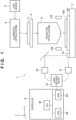
- step S6 the adjustment substrate 200 that has been used is reversed and placed on the substrate holder 101 (step S6).
- a plurality of marks 103 located on the upper surface (first height position) of the adjustment substrate 200 then shift to a position (second height position) on the substrate holder 101 side. That is, the position of each mark on an adjustment substrate is changed between the first and second height positions by reversing the adjustment substrate.
- stages 1 and 2 described above steps S1 to S4 are repeated in the same manner to obtain object-side visual field coordinates (Xi, Yi) and image-side visual field coordinates (X'i, Y'i) (step S7).
- a height sensor using reflected light is mounted in a general exposure apparatus.
- a difference ⁇ h1 between the height of a reference mark 502 on the stage and the height of the upper surface of the substrate 102 (thickness h0) before a process placed on a substrate holder 101 can be measured in advance by reflected light measurement.
- the substrate 102 whose thickness has changed along with process is placed on the substrate holder 101, and a difference ⁇ h2 from the height of the upper surface of the reference mark 502 on the stage is measured in the same manner.
- the height of a reference mark 503 on the substrate holder 101 may be measured instead of the height of the reference mark 502 on the stage.
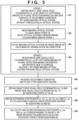
- An exposure method In order to execute this exposure method, information concerning the aberration and telecentricity of a relay optical system 100 is obtained in advance by processing complying with the flowchart of Fig. 4 according to the first embodiment or the method described in the second embodiment.
- a substrate subjected to actual exposure is fed into an exposure apparatus and placed on a mechanism for holding the substrate.
- An imaging optical system 110 then captures an image of a mark 103 provided on the substrate which is obtained via the relay optical system 100.
- a controller 8 then corrects the image shift amount of the observed mark 103 according to equations (7) based on information concerning the aberration and telecentricity of the relay optical system 100 which is read out from a RAM 83.
- the exposure apparatus executes positioning based on information concerning the position of the mark 103 obtained after correction and performs exposure.
Landscapes
- Physics & Mathematics (AREA)
- General Physics & Mathematics (AREA)
- Engineering & Computer Science (AREA)
- Multimedia (AREA)
- Health & Medical Sciences (AREA)
- Environmental & Geological Engineering (AREA)
- Epidemiology (AREA)
- Public Health (AREA)
- Exposure And Positioning Against Photoresist Photosensitive Materials (AREA)
- Length Measuring Devices By Optical Means (AREA)
Applications Claiming Priority (1)
| Application Number | Priority Date | Filing Date | Title |
|---|---|---|---|
| JP2017059923A JP6945316B2 (ja) | 2017-03-24 | 2017-03-24 | 検出装置、パターン形成装置、取得方法、検出方法、および物品製造方法 |
Publications (3)
| Publication Number | Publication Date |
|---|---|
| EP3379333A2 EP3379333A2 (en) | 2018-09-26 |
| EP3379333A3 EP3379333A3 (en) | 2018-10-17 |
| EP3379333B1 true EP3379333B1 (en) | 2023-07-19 |
Family
ID=61616738
Family Applications (1)
| Application Number | Title | Priority Date | Filing Date |
|---|---|---|---|
| EP18000231.3A Active EP3379333B1 (en) | 2017-03-24 | 2018-03-07 | Detection apparatus, pattern forming apparatus, obtaining method, detection method, and article manufacturing method |
Country Status (4)
| Country | Link |
|---|---|
| US (1) | US10545415B2 (enExample) |
| EP (1) | EP3379333B1 (enExample) |
| JP (1) | JP6945316B2 (enExample) |
| CN (1) | CN108681209B (enExample) |
Families Citing this family (6)
| Publication number | Priority date | Publication date | Assignee | Title |
|---|---|---|---|---|
| WO2018152202A1 (en) * | 2017-02-14 | 2018-08-23 | Massachusetts Institute Of Technology | Systems and methods for automated microscopy |
| JP7252322B2 (ja) * | 2018-09-24 | 2023-04-04 | エーエスエムエル ネザーランズ ビー.ブイ. | プロセスツール及び検査方法 |
| JP2020112605A (ja) * | 2019-01-08 | 2020-07-27 | キヤノン株式会社 | 露光装置およびその制御方法、および、物品製造方法 |
| JP7339826B2 (ja) * | 2019-09-19 | 2023-09-06 | キヤノン株式会社 | マーク位置決定方法、リソグラフィー方法、物品製造方法、プログラムおよびリソグラフィー装置 |
| CN113048905B (zh) * | 2019-12-27 | 2022-08-19 | 上海微电子装备(集团)股份有限公司 | 对准标记图像制作方法、对准标记测量方法及测量装置 |
| CN112539706B (zh) * | 2020-12-09 | 2022-09-30 | 深圳友讯达科技股份有限公司 | 一种晶圆薄片切割质量检测设备 |
Family Cites Families (18)
| Publication number | Priority date | Publication date | Assignee | Title |
|---|---|---|---|---|
| JPS5922325A (ja) | 1982-07-29 | 1984-02-04 | Toshiba Corp | 電子ビ−ム描画装置 |
| KR100579603B1 (ko) * | 2001-01-15 | 2006-05-12 | 에이에스엠엘 네델란즈 비.브이. | 리소그래피 장치 |
| US6525805B2 (en) * | 2001-05-14 | 2003-02-25 | Ultratech Stepper, Inc. | Backside alignment system and method |
| JP2003059807A (ja) * | 2001-08-20 | 2003-02-28 | Nikon Corp | 露光方法及び露光装置、並びにデバイス製造方法 |
| TW594431B (en) * | 2002-03-01 | 2004-06-21 | Asml Netherlands Bv | Calibration methods, calibration substrates, lithographic apparatus and device manufacturing methods |
| EP1341046A3 (en) * | 2002-03-01 | 2004-12-15 | ASML Netherlands B.V. | Calibration methods, calibration substrates, lithographic apparatus and device manufacturing methods |
| EP1477861A1 (en) * | 2003-05-16 | 2004-11-17 | ASML Netherlands B.V. | A method of calibrating a lithographic apparatus, an alignment method, a computer program, a lithographic apparatus and a device manufacturing method |
| JP4340638B2 (ja) * | 2004-03-02 | 2009-10-07 | エーエスエムエル ネザーランズ ビー.ブイ. | 基板の表側または裏側に結像するためのリソグラフィ装置、基板識別方法、デバイス製造方法、基板、およびコンピュータプログラム |
| US7420676B2 (en) * | 2004-07-28 | 2008-09-02 | Asml Netherlands B.V. | Alignment method, method of measuring front to backside alignment error, method of detecting non-orthogonality, method of calibration, and lithographic apparatus |
| US7398177B2 (en) * | 2004-10-15 | 2008-07-08 | Asml Netherlands B.V. | Measurement substrate, substrate table, lithographic apparatus, method of calculating an angle of an alignment beam of an alignment system, and alignment verification method |
| US7928591B2 (en) * | 2005-02-11 | 2011-04-19 | Wintec Industries, Inc. | Apparatus and method for predetermined component placement to a target platform |
| US7501215B2 (en) * | 2005-06-28 | 2009-03-10 | Asml Netherlands B.V. | Device manufacturing method and a calibration substrate |
| KR101477833B1 (ko) * | 2007-12-28 | 2014-12-30 | 가부시키가이샤 니콘 | 노광 장치, 이동체 구동 시스템, 패턴 형성 장치 및 노광 방법, 그리고 디바이스 제조 방법 |
| JP2010034331A (ja) * | 2008-07-29 | 2010-02-12 | Canon Inc | 露光装置およびデバイス製造方法 |
| JP5652105B2 (ja) * | 2010-10-13 | 2015-01-14 | 株式会社ニコン | 露光装置 |
| CN103488064B (zh) * | 2012-06-14 | 2015-11-18 | 上海微电子装备有限公司 | 一种背面对准装置及背面对准基底贴片方法 |
| NL2014941A (en) * | 2014-07-16 | 2016-04-12 | Asml Netherlands Bv | Lithographic apparatus, device manufacturing method and associated data processing apparatus and computer program product. |
| DE102015112651B3 (de) * | 2015-07-31 | 2016-07-28 | Carl Zeiss Industrielle Messtechnik Gmbh | Verfahren und Messgerät zum Bestimmen von dimensionalen Eigenschaften eines Messobjekts |
-
2017
- 2017-03-24 JP JP2017059923A patent/JP6945316B2/ja active Active
-
2018
- 2018-03-07 EP EP18000231.3A patent/EP3379333B1/en active Active
- 2018-03-20 US US15/926,258 patent/US10545415B2/en active Active
- 2018-03-22 CN CN201810242026.5A patent/CN108681209B/zh active Active
Also Published As
| Publication number | Publication date |
|---|---|
| EP3379333A3 (en) | 2018-10-17 |
| CN108681209A (zh) | 2018-10-19 |
| JP2018163247A (ja) | 2018-10-18 |
| US20180275535A1 (en) | 2018-09-27 |
| JP6945316B2 (ja) | 2021-10-06 |
| US10545415B2 (en) | 2020-01-28 |
| CN108681209B (zh) | 2021-01-01 |
| EP3379333A2 (en) | 2018-09-26 |
Similar Documents
| Publication | Publication Date | Title |
|---|---|---|
| EP3379333B1 (en) | Detection apparatus, pattern forming apparatus, obtaining method, detection method, and article manufacturing method | |
| KR101087515B1 (ko) | 얼라인먼트 조건 결정 방법 및 장치, 그리고 노광 방법 및장치 | |
| US20020145716A1 (en) | Exposure method and apparatus, and device manufacturing method | |
| JP2009192271A (ja) | 位置検出方法、露光装置、及びデバイス製造方法 | |
| US12241846B2 (en) | Detection apparatus, detection method, exposure apparatus, exposure system, and article manufacturing method | |
| US11947185B2 (en) | Autofocusing method for an imaging device | |
| US9910371B2 (en) | Exposure apparatus, exposure method, and device manufacturing method | |
| CN115628685B (zh) | 关键尺寸的测量方法、设备及关键尺寸的分级定位方法 | |
| US20180107125A1 (en) | Lithography apparatus and article manufacturing method | |
| JP2016100590A (ja) | フォーカス制御方法、パターン転写装置、および物品の製造方法 | |
| US10635005B2 (en) | Exposure apparatus, method thereof, and method of manufacturing article | |
| JP2009170559A (ja) | 露光装置およびデバイス製造方法 | |
| JP3040845B2 (ja) | アライメントマーク | |
| JP4290172B2 (ja) | 伝達特性算出装置及び伝達特性算出方法並びに露光装置 | |
| CN111413850A (zh) | 曝光装置、用于控制曝光装置的方法、以及物品制造方法 | |
| WO2015094818A1 (en) | A method for measuring positions of structures on a mask and thereby determining mask manufacturing errors | |
| US11822233B2 (en) | Image pickup apparatus and focus adjustment method using bending correction to adjust focusing | |
| US11194257B2 (en) | Exposure method, exposure apparatus, method of manufacturing article, and measurement method | |
| JP4891040B2 (ja) | 計測装置、計測方法、露光装置及びデバイス製造方法 | |
| JPH07226359A (ja) | 位置合わせ方法 | |
| JP5922927B2 (ja) | 位置を求める方法、情報処理装置、リソグラフィ装置及び物品の製造方法 | |
| JPH08102438A (ja) | 位置合わせ方法 | |
| JP2017156629A (ja) | 露光方法及び露光装置 |
Legal Events
| Date | Code | Title | Description |
|---|---|---|---|
| PUAI | Public reference made under article 153(3) epc to a published international application that has entered the european phase |
Free format text: ORIGINAL CODE: 0009012 |
|
| STAA | Information on the status of an ep patent application or granted ep patent |
Free format text: STATUS: THE APPLICATION HAS BEEN PUBLISHED |
|
| PUAL | Search report despatched |
Free format text: ORIGINAL CODE: 0009013 |
|
| AK | Designated contracting states |
Kind code of ref document: A2 Designated state(s): AL AT BE BG CH CY CZ DE DK EE ES FI FR GB GR HR HU IE IS IT LI LT LU LV MC MK MT NL NO PL PT RO RS SE SI SK SM TR |
|
| AX | Request for extension of the european patent |
Extension state: BA ME |
|
| AK | Designated contracting states |
Kind code of ref document: A3 Designated state(s): AL AT BE BG CH CY CZ DE DK EE ES FI FR GB GR HR HU IE IS IT LI LT LU LV MC MK MT NL NO PL PT RO RS SE SI SK SM TR |
|
| AX | Request for extension of the european patent |
Extension state: BA ME |
|
| RIC1 | Information provided on ipc code assigned before grant |
Ipc: G03F 9/00 20060101AFI20180912BHEP |
|
| STAA | Information on the status of an ep patent application or granted ep patent |
Free format text: STATUS: REQUEST FOR EXAMINATION WAS MADE |
|
| 17P | Request for examination filed |
Effective date: 20190417 |
|
| RBV | Designated contracting states (corrected) |
Designated state(s): AL AT BE BG CH CY CZ DE DK EE ES FI FR GB GR HR HU IE IS IT LI LT LU LV MC MK MT NL NO PL PT RO RS SE SI SK SM TR |
|
| STAA | Information on the status of an ep patent application or granted ep patent |
Free format text: STATUS: EXAMINATION IS IN PROGRESS |
|
| 17Q | First examination report despatched |
Effective date: 20210716 |
|
| GRAP | Despatch of communication of intention to grant a patent |
Free format text: ORIGINAL CODE: EPIDOSNIGR1 |
|
| STAA | Information on the status of an ep patent application or granted ep patent |
Free format text: STATUS: GRANT OF PATENT IS INTENDED |
|
| INTG | Intention to grant announced |
Effective date: 20230217 |
|
| GRAS | Grant fee paid |
Free format text: ORIGINAL CODE: EPIDOSNIGR3 |
|
| GRAA | (expected) grant |
Free format text: ORIGINAL CODE: 0009210 |
|
| STAA | Information on the status of an ep patent application or granted ep patent |
Free format text: STATUS: THE PATENT HAS BEEN GRANTED |
|
| AK | Designated contracting states |
Kind code of ref document: B1 Designated state(s): AL AT BE BG CH CY CZ DE DK EE ES FI FR GB GR HR HU IE IS IT LI LT LU LV MC MK MT NL NO PL PT RO RS SE SI SK SM TR |
|
| REG | Reference to a national code |
Ref country code: GB Ref legal event code: FG4D |
|
| REG | Reference to a national code |
Ref country code: CH Ref legal event code: EP |
|
| REG | Reference to a national code |
Ref country code: DE Ref legal event code: R096 Ref document number: 602018053473 Country of ref document: DE |
|
| REG | Reference to a national code |
Ref country code: IE Ref legal event code: FG4D |
|
| REG | Reference to a national code |
Ref country code: LT Ref legal event code: MG9D |
|
| REG | Reference to a national code |
Ref country code: NL Ref legal event code: MP Effective date: 20230719 |
|
| REG | Reference to a national code |
Ref country code: AT Ref legal event code: MK05 Ref document number: 1590068 Country of ref document: AT Kind code of ref document: T Effective date: 20230719 |
|
| PG25 | Lapsed in a contracting state [announced via postgrant information from national office to epo] |
Ref country code: NL Free format text: LAPSE BECAUSE OF FAILURE TO SUBMIT A TRANSLATION OF THE DESCRIPTION OR TO PAY THE FEE WITHIN THE PRESCRIBED TIME-LIMIT Effective date: 20230719 |
|
| PG25 | Lapsed in a contracting state [announced via postgrant information from national office to epo] |
Ref country code: GR Free format text: LAPSE BECAUSE OF FAILURE TO SUBMIT A TRANSLATION OF THE DESCRIPTION OR TO PAY THE FEE WITHIN THE PRESCRIBED TIME-LIMIT Effective date: 20231020 |
|
| PG25 | Lapsed in a contracting state [announced via postgrant information from national office to epo] |
Ref country code: IS Free format text: LAPSE BECAUSE OF FAILURE TO SUBMIT A TRANSLATION OF THE DESCRIPTION OR TO PAY THE FEE WITHIN THE PRESCRIBED TIME-LIMIT Effective date: 20231119 |
|
| PG25 | Lapsed in a contracting state [announced via postgrant information from national office to epo] |
Ref country code: SE Free format text: LAPSE BECAUSE OF FAILURE TO SUBMIT A TRANSLATION OF THE DESCRIPTION OR TO PAY THE FEE WITHIN THE PRESCRIBED TIME-LIMIT Effective date: 20230719 Ref country code: RS Free format text: LAPSE BECAUSE OF FAILURE TO SUBMIT A TRANSLATION OF THE DESCRIPTION OR TO PAY THE FEE WITHIN THE PRESCRIBED TIME-LIMIT Effective date: 20230719 Ref country code: PT Free format text: LAPSE BECAUSE OF FAILURE TO SUBMIT A TRANSLATION OF THE DESCRIPTION OR TO PAY THE FEE WITHIN THE PRESCRIBED TIME-LIMIT Effective date: 20231120 Ref country code: NO Free format text: LAPSE BECAUSE OF FAILURE TO SUBMIT A TRANSLATION OF THE DESCRIPTION OR TO PAY THE FEE WITHIN THE PRESCRIBED TIME-LIMIT Effective date: 20231019 Ref country code: LV Free format text: LAPSE BECAUSE OF FAILURE TO SUBMIT A TRANSLATION OF THE DESCRIPTION OR TO PAY THE FEE WITHIN THE PRESCRIBED TIME-LIMIT Effective date: 20230719 Ref country code: LT Free format text: LAPSE BECAUSE OF FAILURE TO SUBMIT A TRANSLATION OF THE DESCRIPTION OR TO PAY THE FEE WITHIN THE PRESCRIBED TIME-LIMIT Effective date: 20230719 Ref country code: IS Free format text: LAPSE BECAUSE OF FAILURE TO SUBMIT A TRANSLATION OF THE DESCRIPTION OR TO PAY THE FEE WITHIN THE PRESCRIBED TIME-LIMIT Effective date: 20231119 Ref country code: HR Free format text: LAPSE BECAUSE OF FAILURE TO SUBMIT A TRANSLATION OF THE DESCRIPTION OR TO PAY THE FEE WITHIN THE PRESCRIBED TIME-LIMIT Effective date: 20230719 Ref country code: GR Free format text: LAPSE BECAUSE OF FAILURE TO SUBMIT A TRANSLATION OF THE DESCRIPTION OR TO PAY THE FEE WITHIN THE PRESCRIBED TIME-LIMIT Effective date: 20231020 Ref country code: FI Free format text: LAPSE BECAUSE OF FAILURE TO SUBMIT A TRANSLATION OF THE DESCRIPTION OR TO PAY THE FEE WITHIN THE PRESCRIBED TIME-LIMIT Effective date: 20230719 Ref country code: AT Free format text: LAPSE BECAUSE OF FAILURE TO SUBMIT A TRANSLATION OF THE DESCRIPTION OR TO PAY THE FEE WITHIN THE PRESCRIBED TIME-LIMIT Effective date: 20230719 |
|
| PG25 | Lapsed in a contracting state [announced via postgrant information from national office to epo] |
Ref country code: PL Free format text: LAPSE BECAUSE OF FAILURE TO SUBMIT A TRANSLATION OF THE DESCRIPTION OR TO PAY THE FEE WITHIN THE PRESCRIBED TIME-LIMIT Effective date: 20230719 |
|
| REG | Reference to a national code |
Ref country code: DE Ref legal event code: R097 Ref document number: 602018053473 Country of ref document: DE |
|
| PG25 | Lapsed in a contracting state [announced via postgrant information from national office to epo] |
Ref country code: ES Free format text: LAPSE BECAUSE OF FAILURE TO SUBMIT A TRANSLATION OF THE DESCRIPTION OR TO PAY THE FEE WITHIN THE PRESCRIBED TIME-LIMIT Effective date: 20230719 |
|
| PG25 | Lapsed in a contracting state [announced via postgrant information from national office to epo] |
Ref country code: SM Free format text: LAPSE BECAUSE OF FAILURE TO SUBMIT A TRANSLATION OF THE DESCRIPTION OR TO PAY THE FEE WITHIN THE PRESCRIBED TIME-LIMIT Effective date: 20230719 Ref country code: RO Free format text: LAPSE BECAUSE OF FAILURE TO SUBMIT A TRANSLATION OF THE DESCRIPTION OR TO PAY THE FEE WITHIN THE PRESCRIBED TIME-LIMIT Effective date: 20230719 Ref country code: ES Free format text: LAPSE BECAUSE OF FAILURE TO SUBMIT A TRANSLATION OF THE DESCRIPTION OR TO PAY THE FEE WITHIN THE PRESCRIBED TIME-LIMIT Effective date: 20230719 Ref country code: EE Free format text: LAPSE BECAUSE OF FAILURE TO SUBMIT A TRANSLATION OF THE DESCRIPTION OR TO PAY THE FEE WITHIN THE PRESCRIBED TIME-LIMIT Effective date: 20230719 Ref country code: DK Free format text: LAPSE BECAUSE OF FAILURE TO SUBMIT A TRANSLATION OF THE DESCRIPTION OR TO PAY THE FEE WITHIN THE PRESCRIBED TIME-LIMIT Effective date: 20230719 Ref country code: CZ Free format text: LAPSE BECAUSE OF FAILURE TO SUBMIT A TRANSLATION OF THE DESCRIPTION OR TO PAY THE FEE WITHIN THE PRESCRIBED TIME-LIMIT Effective date: 20230719 Ref country code: SK Free format text: LAPSE BECAUSE OF FAILURE TO SUBMIT A TRANSLATION OF THE DESCRIPTION OR TO PAY THE FEE WITHIN THE PRESCRIBED TIME-LIMIT Effective date: 20230719 |
|
| PLBE | No opposition filed within time limit |
Free format text: ORIGINAL CODE: 0009261 |
|
| STAA | Information on the status of an ep patent application or granted ep patent |
Free format text: STATUS: NO OPPOSITION FILED WITHIN TIME LIMIT |
|
| 26N | No opposition filed |
Effective date: 20240422 |
|
| PG25 | Lapsed in a contracting state [announced via postgrant information from national office to epo] |
Ref country code: SI Free format text: LAPSE BECAUSE OF FAILURE TO SUBMIT A TRANSLATION OF THE DESCRIPTION OR TO PAY THE FEE WITHIN THE PRESCRIBED TIME-LIMIT Effective date: 20230719 |
|
| REG | Reference to a national code |
Ref country code: CH Ref legal event code: PL |
|
| PG25 | Lapsed in a contracting state [announced via postgrant information from national office to epo] |
Ref country code: BG Free format text: LAPSE BECAUSE OF FAILURE TO SUBMIT A TRANSLATION OF THE DESCRIPTION OR TO PAY THE FEE WITHIN THE PRESCRIBED TIME-LIMIT Effective date: 20230719 |
|
| PG25 | Lapsed in a contracting state [announced via postgrant information from national office to epo] |
Ref country code: LU Free format text: LAPSE BECAUSE OF NON-PAYMENT OF DUE FEES Effective date: 20240307 |
|
| PG25 | Lapsed in a contracting state [announced via postgrant information from national office to epo] |
Ref country code: MC Free format text: LAPSE BECAUSE OF FAILURE TO SUBMIT A TRANSLATION OF THE DESCRIPTION OR TO PAY THE FEE WITHIN THE PRESCRIBED TIME-LIMIT Effective date: 20230719 |
|
| GBPC | Gb: european patent ceased through non-payment of renewal fee |
Effective date: 20240307 |
|
| PG25 | Lapsed in a contracting state [announced via postgrant information from national office to epo] |
Ref country code: MC Free format text: LAPSE BECAUSE OF FAILURE TO SUBMIT A TRANSLATION OF THE DESCRIPTION OR TO PAY THE FEE WITHIN THE PRESCRIBED TIME-LIMIT Effective date: 20230719 Ref country code: LU Free format text: LAPSE BECAUSE OF NON-PAYMENT OF DUE FEES Effective date: 20240307 Ref country code: BG Free format text: LAPSE BECAUSE OF FAILURE TO SUBMIT A TRANSLATION OF THE DESCRIPTION OR TO PAY THE FEE WITHIN THE PRESCRIBED TIME-LIMIT Effective date: 20230719 |
|
| REG | Reference to a national code |
Ref country code: BE Ref legal event code: MM Effective date: 20240331 |
|
| PG25 | Lapsed in a contracting state [announced via postgrant information from national office to epo] |
Ref country code: BE Free format text: LAPSE BECAUSE OF NON-PAYMENT OF DUE FEES Effective date: 20240331 |
|
| PG25 | Lapsed in a contracting state [announced via postgrant information from national office to epo] |
Ref country code: GB Free format text: LAPSE BECAUSE OF NON-PAYMENT OF DUE FEES Effective date: 20240307 |
|
| PG25 | Lapsed in a contracting state [announced via postgrant information from national office to epo] |
Ref country code: IE Free format text: LAPSE BECAUSE OF NON-PAYMENT OF DUE FEES Effective date: 20240307 |
|
| PG25 | Lapsed in a contracting state [announced via postgrant information from national office to epo] |
Ref country code: IE Free format text: LAPSE BECAUSE OF NON-PAYMENT OF DUE FEES Effective date: 20240307 Ref country code: GB Free format text: LAPSE BECAUSE OF NON-PAYMENT OF DUE FEES Effective date: 20240307 Ref country code: BE Free format text: LAPSE BECAUSE OF NON-PAYMENT OF DUE FEES Effective date: 20240331 Ref country code: CH Free format text: LAPSE BECAUSE OF NON-PAYMENT OF DUE FEES Effective date: 20240331 |
|
| PG25 | Lapsed in a contracting state [announced via postgrant information from national office to epo] |
Ref country code: CY Free format text: LAPSE BECAUSE OF FAILURE TO SUBMIT A TRANSLATION OF THE DESCRIPTION OR TO PAY THE FEE WITHIN THE PRESCRIBED TIME-LIMIT; INVALID AB INITIO Effective date: 20180307 |
|
| PG25 | Lapsed in a contracting state [announced via postgrant information from national office to epo] |
Ref country code: HU Free format text: LAPSE BECAUSE OF FAILURE TO SUBMIT A TRANSLATION OF THE DESCRIPTION OR TO PAY THE FEE WITHIN THE PRESCRIBED TIME-LIMIT; INVALID AB INITIO Effective date: 20180307 |
|
| PG25 | Lapsed in a contracting state [announced via postgrant information from national office to epo] |
Ref country code: TR Free format text: LAPSE BECAUSE OF FAILURE TO SUBMIT A TRANSLATION OF THE DESCRIPTION OR TO PAY THE FEE WITHIN THE PRESCRIBED TIME-LIMIT Effective date: 20230719 |
|
| PGFP | Annual fee paid to national office [announced via postgrant information from national office to epo] |
Ref country code: DE Payment date: 20260219 Year of fee payment: 9 |
|
| PGFP | Annual fee paid to national office [announced via postgrant information from national office to epo] |
Ref country code: IT Payment date: 20260219 Year of fee payment: 9 |
|
| PGFP | Annual fee paid to national office [announced via postgrant information from national office to epo] |
Ref country code: FR Payment date: 20260220 Year of fee payment: 9 |