EP3379275A1 - Semiconductor integrated circuit and semiconductor integrated circuit diagnosis method - Google Patents
Semiconductor integrated circuit and semiconductor integrated circuit diagnosis method Download PDFInfo
- Publication number
- EP3379275A1 EP3379275A1 EP17188108.9A EP17188108A EP3379275A1 EP 3379275 A1 EP3379275 A1 EP 3379275A1 EP 17188108 A EP17188108 A EP 17188108A EP 3379275 A1 EP3379275 A1 EP 3379275A1
- Authority
- EP
- European Patent Office
- Prior art keywords
- scan
- value
- scan chains
- retention
- output data
- Prior art date
- Legal status (The legal status is an assumption and is not a legal conclusion. Google has not performed a legal analysis and makes no representation as to the accuracy of the status listed.)
- Withdrawn
Links
Images


Classifications
-
- G—PHYSICS
- G01—MEASURING; TESTING
- G01R—MEASURING ELECTRIC VARIABLES; MEASURING MAGNETIC VARIABLES
- G01R31/00—Arrangements for testing electric properties; Arrangements for locating electric faults; Arrangements for electrical testing characterised by what is being tested not provided for elsewhere
- G01R31/28—Testing of electronic circuits, e.g. by signal tracer
- G01R31/2851—Testing of integrated circuits [IC]
-
- G—PHYSICS
- G01—MEASURING; TESTING
- G01R—MEASURING ELECTRIC VARIABLES; MEASURING MAGNETIC VARIABLES
- G01R31/00—Arrangements for testing electric properties; Arrangements for locating electric faults; Arrangements for electrical testing characterised by what is being tested not provided for elsewhere
- G01R31/28—Testing of electronic circuits, e.g. by signal tracer
- G01R31/317—Testing of digital circuits
- G01R31/3181—Functional testing
- G01R31/3185—Reconfiguring for testing, e.g. LSSD, partitioning
- G01R31/318533—Reconfiguring for testing, e.g. LSSD, partitioning using scanning techniques, e.g. LSSD, Boundary Scan, JTAG
- G01R31/318544—Scanning methods, algorithms and patterns
-
- G—PHYSICS
- G01—MEASURING; TESTING
- G01R—MEASURING ELECTRIC VARIABLES; MEASURING MAGNETIC VARIABLES
- G01R31/00—Arrangements for testing electric properties; Arrangements for locating electric faults; Arrangements for electrical testing characterised by what is being tested not provided for elsewhere
- G01R31/28—Testing of electronic circuits, e.g. by signal tracer
- G01R31/317—Testing of digital circuits
- G01R31/31724—Test controller, e.g. BIST state machine
-
- G—PHYSICS
- G01—MEASURING; TESTING
- G01R—MEASURING ELECTRIC VARIABLES; MEASURING MAGNETIC VARIABLES
- G01R31/00—Arrangements for testing electric properties; Arrangements for locating electric faults; Arrangements for electrical testing characterised by what is being tested not provided for elsewhere
- G01R31/28—Testing of electronic circuits, e.g. by signal tracer
- G01R31/317—Testing of digital circuits
- G01R31/3181—Functional testing
- G01R31/3185—Reconfiguring for testing, e.g. LSSD, partitioning
- G01R31/318533—Reconfiguring for testing, e.g. LSSD, partitioning using scanning techniques, e.g. LSSD, Boundary Scan, JTAG
- G01R31/318536—Scan chain arrangements, e.g. connections, test bus, analog signals
-
- G—PHYSICS
- G01—MEASURING; TESTING
- G01R—MEASURING ELECTRIC VARIABLES; MEASURING MAGNETIC VARIABLES
- G01R31/00—Arrangements for testing electric properties; Arrangements for locating electric faults; Arrangements for electrical testing characterised by what is being tested not provided for elsewhere
- G01R31/28—Testing of electronic circuits, e.g. by signal tracer
- G01R31/317—Testing of digital circuits
- G01R31/3181—Functional testing
- G01R31/3185—Reconfiguring for testing, e.g. LSSD, partitioning
- G01R31/318533—Reconfiguring for testing, e.g. LSSD, partitioning using scanning techniques, e.g. LSSD, Boundary Scan, JTAG
- G01R31/318566—Comparators; Diagnosing the device under test
-
- G—PHYSICS
- G01—MEASURING; TESTING
- G01R—MEASURING ELECTRIC VARIABLES; MEASURING MAGNETIC VARIABLES
- G01R31/00—Arrangements for testing electric properties; Arrangements for locating electric faults; Arrangements for electrical testing characterised by what is being tested not provided for elsewhere
- G01R31/28—Testing of electronic circuits, e.g. by signal tracer
- G01R31/317—Testing of digital circuits
- G01R31/3181—Functional testing
- G01R31/3185—Reconfiguring for testing, e.g. LSSD, partitioning
- G01R31/318533—Reconfiguring for testing, e.g. LSSD, partitioning using scanning techniques, e.g. LSSD, Boundary Scan, JTAG
- G01R31/318575—Power distribution; Power saving
-
- G—PHYSICS
- G06—COMPUTING OR CALCULATING; COUNTING
- G06F—ELECTRIC DIGITAL DATA PROCESSING
- G06F11/00—Error detection; Error correction; Monitoring
- G06F11/22—Detection or location of defective computer hardware by testing during standby operation or during idle time, e.g. start-up testing
- G06F11/26—Functional testing
- G06F11/267—Reconfiguring circuits for testing, e.g. LSSD, partitioning
Definitions
- Embodiments described herein relate generally to a semiconductor integrated circuit and a semiconductor integrated circuit diagnosis method.
- a logic BIST may be conducted not only in initial diagnosis at the time of start-up of a semiconductor device, but also in regular diagnosis during operation of the semiconductor device.
- Each retention flip-flop includes a main unit and a retention section, and before power shut-down, can save data in the retention section and after power recovery, restore the data in the main unit from the saved data in the retention section.
- retention flip-flops are used for diagnosis of a semiconductor device, if a defect or a failure occurs in retention performance of the retention sections and/or save operation and restoration operation of the retention flip-flops, data is not correctly restored. Conventionally, no method for diagnosis of such retention performance of retention sections and save operation and restoration operation of retention flip-flops has been proposed.
- a semiconductor integrated circuit includes: at least one scan chain including a retention flip-flop; and a diagnosis circuit configured to perform restoration of data saved in a retention section of the retention flip-flop by reading the data from the retention section, and after the restoration of the data, perform diagnosis of the retention flip-flop by performing comparison to determine whether or not a first value of a first output data string obtained as a result of a scan shift in the at least one scan chain before the save and a second value of a second output data string obtained as a result of a scan shift of the data in the at least one scan chain after the restoration agree with each other.
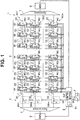
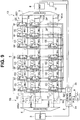
- Fig. 1 is a circuit block diagram of a semiconductor device according to a first embodiment.
- a semiconductor device 1 is a semiconductor integrated circuit including a plurality of combination circuits CC each configuring a logic section, and the semiconductor device 1 has a logic BIST function.
- the semiconductor device 1 includes a control section 2, a pattern generation circuit (PRPG: pseudo random pattern generator) 3, a decompressor 4, a selector 5, a plurality of scan chains 6, a compressor 7, a multiple input signature register (hereinafter abbreviated as MISR) 8 in addition to the plurality of combination circuits CC.
- the control section 2 includes a logic BIST controller 2a for a logic BIST.
- control section 2 can output a power control signal PCS for controlling a power switch 9 for controlling supply of power to the semiconductor device 1, which is a semiconductor chip.
- the plurality of scan chains 6 for a logic BIST are formed. Only a single scan chain 6 may be provided.
- the plurality of scan chains 6 include m (m is a positive integer) scan chains SC1 to SCm.
- m is a positive integer
- one arbitrary scan chain or all scan chains of the m scan chains SC1 to SCm refer to scan chain(s) SC.
- each of the scan chains SC1 to SCm configures a scan shift path formed by cascade connection of a plurality of retention flip-flops RF in the logic sections.
- Each retention flip-flop RF is disposed between combination circuits CC, and can retain an inner state of the relevant logic section.
- each retention flip-flop RF is provided by a configuration including a main unit MU and a retention section BL.
- the main unit MU which is required to perform high-speed operation, includes a flip-flop including a transistor having a low threshold voltage.
- the retention section BL includes a flip-flop including a transistor having a high threshold voltage. Since the threshold voltage of the flip-flop in the main unit MU is low, the flip-flop operates at high speed but causes large leakage current. The flip-flop of the retention section BL operates slowly and retains the inner state with small leakage current.
- the main unit MU includes six inputs, which are a D input, a shift-in (SI) input, a shift enable (SE) input, a clock (CLK) input, a store (S) input and a restore (R) input, and a Q output.
- SI shift-in
- SE shift enable
- CLK clock
- S store
- R restore
- a plurality of retention flip-flops RF are connected in a cascade form so that a Q output of a retention flip-flop RF is supplied to a shift-in (SI) input of a next retention flip-flop RF.
- SI shift-in
- the D input which is an output of a combination circuit CC, is retained in response to a clock (CLK) input, and is outputted as a Q output.
- the shift-in (SI) input is retained in response to a shift enable (SE) input, and is outputted to the Q output.
- the retention flip-flop RF retains the Q output in the retention section BL in response to the store (S) input.
- the retention flip-flop RF reads and retains data retained in the retention section BL and outputs the data as the Q output, in response to the restore (R) input.
- the control section 2 is a controller including a logic circuit, the controller performing processing for initial diagnosis of the logic sections at the time of start-up of the semiconductor device 1 and retention flip-flop diagnosis processing for confirming whether or not any defect occurs in, e.g., retention performance of the retention sections BL in the plurality of retention flip-flops RF.
- the initial diagnosis of the logic sections is performed by the logic BIST controller 2a.
- control section 2 may be configured by a central processing unit (CPU), a ROM and a RAM so that programs stored in the ROM are executed by the CPU to perform processing for diagnosis of the logic sections and processing for diagnosis of the plurality of retention flip-flops RF.
- CPU central processing unit
- ROM read-only memory
- RAM random access memory
- the pattern generation circuit 3 is a pseudo random pattern generation circuit (PRPG) configured to generate a pseudo random pattern as a test pattern.
- the pseudo random pattern is pseudo random number data.
- the decompressor 4 decompresses the pseudo random number data and supplies the pseudo random number data to the selector 5.
- the selector 5 includes a plurality of switches SW1 to SWm.
- the respective switches SW1 to SWm are provided corresponding to the plurality of scan chains SC1 to SCm, and are provided at respective test pattern input sections of the scan chains SC1 to SCm.
- Each of the switches SW1 to SWm is a circuit configured to select a signal from the pattern generation circuit 3, "0" or “1 ", and output the selected signal to the relevant scan chain SC. Which signal to be selected and outputted by each of the switches SW1 to SWm is determined based on a selection signal SS from the control section 2. In other words, each of the switches SW1 to SWm configures a switching circuit configured to perform switching so as to fix inputs to the plurality of scan chains SC to 1 or 0, which is a predetermined value.
- each of the switches SW1 to SWm selects "0" or "1", which is a fixed value, and supplies the selected "0" or "1" to the input section of the relevant scan chain SC.
- the compressor 7 compresses the output data from the plurality of scan chains SC1 to SCm and outputs the data to the MISR 8.
- the MISR 8 is an output response compressor including a register configured to be capable of retaining data with a width of a plurality of bits, the data storing an output of the compressor 7.
- a value (fixed value) of the MISR 8 where a scan shift is performed when a value of each retention flip-flop RF is "0" and a value (fixed value) of the MISR 8 where a scan shift is performed when the value of each retention flip-flop RF is "1" can be obtained by calculation, the control section 2 retains these two fixed values in advance in the circuit as expected values.
- control section 2 compares output data from the MISR 8 and these expected values to determine whether or not a failure occurs in the semiconductor device 1.
- control section 2 controls the logic BIST controller 2a, the pattern generation circuit 3 and the selector 5 to perform the initial diagnosis, and compares an output of the MISR 8 and expected values for initial diagnosis of the logic sections to perform diagnosis of the semiconductor device 1.
- a result of the diagnosis is outputted by the control section 2 to another CPU in the semiconductor device 1 or the outside.
- a test pattern for diagnosis of the logic sections is inputted from the selector 5 to each scan chain SC, and the logic BIST controller 2a performs diagnosis of the logic sections based on the test pattern.
- test pattern data from the pattern generation circuit 3 is set in the logic sections via the respective scan shift paths.
- a test pattern is set in the plurality of retention flip-flops RF via the scan shift paths, and initial diagnosis of the logic sections is then performed by determining whether or not the value of the MISR 8 is a predetermined expected value.
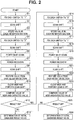
- FIG. 2 is a flowchart illustrating an example of a flow of processing for initial diagnosis of the retention flip-flops RF.
- the control section 2 controls operation of the selector 5 and the plurality of scan chains 6 at the time of diagnosis of the retention flip-flops RF.
- the semiconductor device 1 performs initial diagnosis of the respective retention flip-flops RF, which is described below, after or before performance of the above-described initial diagnosis using a logic BIST.
- diagnosis of whether or not retention performance of the retention sections BL in the retention flip-flops RF and save operation and restoration operation of the retention flip-flops RF function correctly is performed.
- control section 2 when a logic BIST of logic sections that are general circuits is conducted, the control section 2 outputs a selection signal SS for switching of the respective switches SW1 to SWm to the selector 5 to select the signal from the pattern generation circuit 3 and the decompressor 4 and supply the signal to the respective scan chains 6.
- the control section 2 outputs a selection signal SS for switching of the respective switches SW1 to SWm to the selector 5 so as to select a fixed value of "0" or "1" and supply the fixed value to the respective scan chains 6.
- control section 2 when the control section 2 performs diagnosis of retention performance of the retention sections BL in the respective retention flip-flops RF and save operation and restoration operation of the respective retention flip-flops RF, the control section 2 first outputs a selection signal SS for fixing an output of each switch SW to "1" to each switch SW (step (hereinafter abbreviated as "S") 1).
- the control section 2 supplies a shift enable (SE) signal to the respective retention flip-flops RF a predetermined number of times to perform a scan shift so that each retention flip-flop RF of each scan chain SC retains "1" (S2).
- SE shift enable
- the predetermined number of times is a number of times required to retain "1" in each retention flip-flop RF in each scan chain SC.
- the control section 2 supplies a store (S) signal to each retention flip-flop RF to store a value of the Q output in the retention section BL (S3).
- control section 2 outputs a selection signal SS for fixing an output of each switch SW to "0" to each switch SW (S4).
- the control section 2 supplies a shift enable (SE) signal to the respective retention flip-flops RF a predetermined number of times to perform a scan shift so that each retention flip-flop RF in each scan chain SC retains "0" (S5).
- SE shift enable
- the number of times is a number of times that is equal to the number of times required to retain "1" in each retention flip-flop RF in each scan chain SC.
- the control section 2 outputs a power control signal PCS for power-off to turn the power switch 9 off for power shut-down (S6).
- control section 2 outputs a power control signal PCS for power-on to turn the power switch 9 on for power recovery (S7).
- control section 2 supplies a shift enable (SE) signal to the respective retention flip-flops RF a predetermined number of times to perform a scan shift (S8).
- SE shift enable
- S8 scan shift
- the control section 2 supplies a restore (R) signal to each retention flip-flop RF to restore the value from the retention section BL (S9).
- the control section 2 clears the value of the MISR 8 and then supplies a shift enable (SE) signal to the respective retention flip-flops RF a predetermined number of times to perform a scan shift (S10).
- SE shift enable
- the control section 2 reads the value of the register in the MISR 8 and compares the value of the MISR 8 and a predetermined expected value (S 11).
- S 11 a predetermined expected value
- the control section 2 determines whether or not a result of the comparison between the value of the MISR 8 and the predetermined expected value is "OK", that is, whether or not the value of the MISR 8 and the predetermined expected value agree with each other (S12), and if the result of the comparison is "NG" (S12: NO), the control section 2 determines that a result of the initial diagnosis is "NG” (S 13).
- control section 2 If the result of the comparison between the value of the MISR 8 and the predetermined expected value is "OK" (S12: YES), the control section 2 outputs a selection signal SS for fixing an output of each switch SW to "0" to each switch SW (S14).
- the control section 2 supplies a shift enable (SE) signal to the respective retention flip-flops RF a predetermined number of times to perform a scan shift (S 15) so that each retention flip-flop RF of each scan chain SC retains "0". As a result of the processing in S15, "0" is retained in each switch SW.
- SE shift enable
- the control section 2 supplies a store (S) signal to each retention flip-flop RF to store the value of the Q output in the retention section BL (S16).
- control section 2 outputs a selection signal SS for fixing the output of each switch SW to "1" to each switch SW (S17).
- the control section 2 supplies a shift enable (SE) signal to the respective retention flip-flops RF a predetermined number of times to perform a scan shift so that each retention flip-flop RF in each scan chain SC retains "1" (S18). As a result of the processing in S18, "1" is retained in each switch SW.
- SE shift enable
- the control section 2 outputs a power control signal PCS to turn the power switch 9 off for power shut-down (S 19).
- control section 2 outputs a power control signal PCS to turn the power switch 9 on for power recovery (S20).
- control section 2 supplies a shift enable (SE) signal to the respective retention flip-flops RF the predetermined number of times to perform a scan shift (S21).
- SE shift enable
- control section 2 supplies a restore (R) signal to the respective retention flip-flops RF to restore the data from the retention sections BL (S22).
- the control section 2 clears the data in the MISR 8 and subsequently supplies a shift enable (SE) signal to the respective retention flip-flops RF the predetermined number of times to perform a scan shift (S23).
- SE shift enable
- the control section 2 reads the value of the register in the MISR 8 and compares the value of the MISR 8 and a predetermined expected value (S24).
- S24 a predetermined expected value
- the control section 2 determines whether or not a result of the comparison between the value of the MISR 8 and the predetermined expected value is "OK", that is, the value of the MISR 8 and the predetermined expected value agree with each other (S25), and if the result of the comparison is "NG" (S25: NO), the control section 2 determines that a result of the initial diagnosis is "NG” (S 13).
- control section 2 determines that the result of the initial diagnosis is "OK" (S26).
- control section 2 configures a diagnosis circuit configured to perform data restoration by restoring data (0 or 1) saved in the retention sections BL in the respective retention flip-flops RF from the retention sections BL, and after the data restoration, perform diagnosis of the retention flip-flops RF by performing comparison to determine whether or not a first value (expected value) of an output data string obtained as a result of a scan shift in the plurality of scan chains SC before the save, and a second value of an output data string obtained as a result of a scan shift of data in the plurality of scan chains SC after the restoration agree with each other.
- a diagnosis circuit configured to perform data restoration by restoring data (0 or 1) saved in the retention sections BL in the respective retention flip-flops RF from the retention sections BL, and after the data restoration, perform diagnosis of the retention flip-flops RF by performing comparison to determine whether or not a first value (expected value) of an output data string obtained as a result of a scan shift in the plurality of scan chains SC before the save, and a second value of an output data
- the first value is an expected value of an output data string obtained by setting of a predetermined value (0 or 1) in inputs of the plurality of scan chains SC via the selector 5 and a subsequent scan shift of the predetermined value in the plurality of scan chains SC.
- the second value is a value of an output data string obtained by input of the predetermined value (0 or 1) restored from the retention sections BL to the plurality of can chains SC and a subsequent scan shift.
- control section 2 which is a diagnosis circuit, performs diagnosis of the retention flip-flops RF by performing comparison to determine whether or not the first value and the second value agree with each other when the inputs to the plurality of scan chains SC are fixed to either one of "0" and "1" by the selector 5 and then performs diagnosis of the retention flip-flops RF by performing comparison to determine whether or not the first value and the second value agree with each other when the inputs to the plurality of scan chains SC are fixed to another of "0" and "1" by the selector 5.
- the above-described embodiment enables provision of a semiconductor device and a semiconductor device diagnosis method capable of performing diagnosis of whether or not a defect or a failure occurs in retention performance of retention sections in retention flip-flops and save operation and restoration operation of the retention flip-flop, as initial diagnosis.
- restoration is performed after causing the retention flip-flops RF to retain each of "0” and “1 ", and a value of the MISR 8 and an expected value are compared, and thus, diagnosis of whether or not the retention section BL of each retention flip-flop RF can reliably retain both logical values of "0" and "1" can be performed.
- processing for restoration from the retention sections BL is performed, enabling determination of whether or not a failure occurs due to a transition failure in the retention sections BL.
- S1 to S12 may further be performed after S1 to S25 are performed in Fig. 2 .
- each switch SW can select "0" or "1"
- a toggle flip-flop may be used in consideration of interference with an adjacent flip-flop.
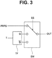
- Fig. 3 is a diagram illustrating an example configuration of a switch using a toggle flip-flop.
- Fig. 3 illustrates a configuration of one switch SW in the selector 5.
- the switch SW allows inputs of a test pattern from the pattern generation circuit 3 and two outputs of a toggle flip-flop TF, and the switch SW selects any of the three inputs, and outputs the selected input as an output signal OUT.
- the toggle flip-flop TF outputs a Q output and an inversion output of the Q output in response to an input T.
- the two outputs of the toggle flip-flop TF that is, the Q output and the inversion output of the Q output are alternately selected and outputted in response to a selection signal SS. Therefore, different values are retained in adjacent retention flip-flops RF.
- the power shut-down may be omitted if the retention flip-flop RF are mounted for retention and restoration for regular diagnosis of the retention flip-flops RF.
- control section 2 performs determination of agreement with an expected value using the MISR 8 configured to compress an output data string from the plurality of scan chains SC, whether or not values corresponding to fixed values "0" and "1" are obtained may be determined, without using the MISR 8.
- the first embodiment relates to a semiconductor device capable of performing initial diagnosis of respective retention flip-flops RF
- a second embodiment relates to a semiconductor device capable of performing regular diagnosis of respective retention flip-flops RF.
- Fig. 4 is a circuit block diagram of a semiconductor device according to a second embodiment.
- a semiconductor device 1A according to the second embodiment has a configuration that is similar to the configuration of the semiconductor device 1 according to the first embodiment, and thus, in Fig. 4 , components that are the same as the components of the semiconductor device 1 according to the first embodiment are provided with reference numerals that are the same as reference numerals in the first embodiment and description of the components will be omitted, and only components that are different from components in the first embodiment will be described.
- a selector 5A is provided at input sections of a plurality of scan chains SC in the semiconductor device 1 A according to the second embodiment.
- the selector 5A includes a plurality of switches SWa1 to SWam.
- the respective switches SWa1 to SWam are provided corresponding to a plurality of scan chains SC1 to SCm, and provided at test pattern input sections of the respective scan chains SC1 to SCm.
- Each of the switches SWa1 to SWam is a circuit configured to select either a signal from a pattern generation circuit 3 or a final output signal from a relevant scan chain SC and output the selected signal to the relevant scan chain SC. Which signal to be selected and outputted by the respective switches SWa1 to SWam is determined based on a selection signal SS from a control section 2. In other words, each of the switches SWa1 to SWam configures a switching circuit configured to fix an input of a relevant scan chain SC to an output data string of the relevant scan chain SC.
- the signal from the pattern generation circuit 3 is selected and outputted to the scan chains SC.
- the respective switches SWa1 to SWam select final output signals from the respective scan chains SC and supply the final output signals to the input sections of the scan chains SC.
- An output of each scan chain SC is supplied to an MISR 8 via a compressor 7.
- a value of the MISR 8 can be stored in a register 10 in response to a control signal (not illustrated) from the control section 2. Then, the control section 2 can read the value stored in the register 10.
- control section 2 saves data in retention sections BL of the plurality of retention flip-flops RF and then performs regular diagnosis of the logic sections. After the regular diagnosis, the operation of the semiconductor device 1 A is resumed after restoration of the saved data in the main units MU. A result of the diagnosis is outputted by the control section 2 to another CPU in the semiconductor device 1A or the outside.
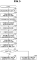
- FIG. 5 is a flowchart illustrating an example of a flow of processing for regular diagnosis of the retention flip-flops RF.
- control section 2 controls operation of the selector 5A and the plurality of scan chains 6.
- the semiconductor device 1A performs below-described regular diagnosis of the respective retention flip-flops RF after or before performance of regular diagnosis using a logic BIST.
- diagnosis of whether or not retention performance of the retention sections BL of the retention flip-flops RF and save operation and restoration operation of the retention flip-flops RF correctly function is performed.
- the control section 2 outputs a selection signal SS for performing switching of the respective switches SWa1 to SWam to the selector 5A so as to select a signal from the pattern generation circuit 3 and a decompressor 4 and supply the signal to the input sections of the respective scan chains 6.
- the control section 2 outputs a selection signal SS for performing switching of the respective switches SWa1 to SWam to the selector 5A so as to select final output signals, that is, shift-out signals, from the respective scan chains SC and supply the final output signals to the input sections of the respective scan chains 6.
- the control section 2 fixes the respective switches SWa1 to SWam to a shift-out (S31) so that inputs of the respective scan chains SC are shift-out signals that are final output signals of the respective scan chains, before power shut-down or before transition to store processing before start of regular diagnosis of the logic sections.
- S31 shift-out
- switching of the respective switches SWa1 to SWam is performed so that the final output signals of the respective scan chains SC are inputted to the input sections of the respective scan chains SC via feedback lines FB.
- the control section 2 clears the MISR 8 and performs a scan shift (S32).
- the scan shift is performed by supplying a shift enable (SE) signal to the respective retention flip-flops RF a predetermined number of times.
- SE shift enable
- the predetermined number of times is a number of times required for data in the respective retention flip-flops RF in the respective scan chains SC to retain respective values retained when the operation of the semiconductor device 1A is interrupted.
- control section 2 stores a value of a result in the MISR 8 obtained as a result of the scan shift in S32, in a register 10 (S33).
- the value of the MISR 8 obtained by the shift-out here is a value that is based on values retained in the main units MU of the respective retention flip-flops RF when the semiconductor device 1A is interrupted, and is retained in the register 10.
- the values retained in the main units MU of the respective retention flip-flops RF return to original values before the shift since the respective data are shifted around the respective scan chains SC.
- control section 2 performs store processing on the respective retention flip-flops RF to store the values of the main units MU in the retention sections BL (S34).
- control section 2 shuts down the power (S35).
- control section 2 may perform regular diagnosis of the logic sections.
- regular diagnosis is performed, the respective switches SWa are switched to the decompressor 4 side.
- the control section 2 performs power recovery (S36). Note that, when the regular diagnosis of the logic sections is finished, the values of the main units MU have been changed.
- control section 2 supplies a restore (R) signal to the respective retention flip-flops RF to restore values from the retention sections BL (S37). If no failure occurs in the retention flip-flops RF, the main units MU should be restored to a state before the power shut-down or before start of the regular diagnosis of the logic sections.
- R restore
- control section 2 clears the value of the MISR 8, performs a scan shift (S38) and compares the value of the register 10 and a result of the MISR 8 (S39).
- the control section 2 determines whether or not a result of the comparison between the value of the register 10 and the value of the MISR 8 is "OK", that is, the value of the MISR 8 and the value of the register 10 agree with each other (S40), and if the result of the comparison is "NG" (S40: NO), the control section 2 determines that a result of the regular diagnosis is "NG" (S41).
- control section 2 determines that the result of the regular diagnosis is "OK" (S42).
- results of the restore are equal to values of the main units MU before the store.
- the scan shift causes the data of the values to be shifted around the respective scan chains and the main units MU of the respective retention flip-flops RF return to respective original values, the data can be used as restored data immediately after re-start of the semiconductor device 1A.
- control section 2 configures a diagnosis circuit configured to perform data restoration by restoring data saved in the retention sections BL of the respective retention flip-flops RF (data when operation of the semiconductor device 1A is interrupted) from the retention sections BL, and after the data restoration, perform diagnosis of the retention flip-flops RF by performing comparison to determine whether or not a first value of an output data string obtained as a result of a scan shift in the plurality of scan chains SC before the save (data when operation of the semiconductor device 1A is interrupted) and a second value of an output data string obtained as a result of a scan shift of data in the plurality of scan chains SC after the restoration agree with each other.
- the first value is a value obtained as a result of a scan shift of an output data string of the plurality of scan chains SC, the output data string being inputted from the selector 5.
- the second value is a value of an output data string obtained as a result of a scan shift of data restored from the retention sections BL.
- a semiconductor device and a semiconductor device diagnosis method capable of performing diagnosis of whether or not a defect or a failure occurs in retention performance of retention sections of retention flip-flops and save operation and restoration operation of the retention flip-flops as regular diagnosis can be provided.
- FIG. 5A is a flowchart illustrating another example of a flow of processing for regular diagnosis of the retention flip-flops RF.
- steps of the processing that are the same as the steps in Fig. 5 are provided with step numbers that are the same as the step numbers in Fig. 5 , and description of the steps will be omitted.
- control section 2 before the processing in S32, the control section 2 performs subjects the respective retention flip-flops RF to store processing to store values of the main units MU in the respective retention sections BL (S43). Then, after the processing in S33, the control section 2 performs power shut-down (S35).
- the processing after S35 is similar to the processing in Fig. 5 , and if it is determined in S42 that a result of the regular diagnosis is "OK", the control section 2 supplies a restore (R) signal to the respective retention flip-flops RF to restore the values from the retention sections BL (S44).
- the processing in Fig. 5A also enables regular diagnosis of the retention flip-flops RF.
- the first embodiment relates to a semiconductor device capable of performing initial diagnosis of respective retention flip-flops RF and the second embodiment relates to a semiconductor device capable of performing regular diagnosis of respective retention flip-flops RF, the third embodiment relates to a semiconductor device capable of performing both initial diagnosis and regular diagnosis of respective retention flip-flops RF.
- Fig. 6 is a circuit block diagram of a semiconductor device according to a third embodiment.
- a semiconductor device 1 B according to a third embodiment has a configuration that is similar to the configuration of the semiconductor device 1A according to the second embodiment, and thus, in Fig. 6 , components that are the same as the components of the semiconductor device 1A according to the second embodiment are provided with reference numerals that are the same as reference numerals of the components of the semiconductor device 1A, and description of the components will be omitted, and only components that are different from the components of the semiconductor device 1 A will be described.
- a selector 5B is provided at input sections of a plurality of scan chains SC in the semiconductor device 1B according to the third embodiment.
- the selector 5B includes a plurality of switches SWb1 to SWbm.
- the respective switches SWb1 to SWbm are provided corresponding to the plurality of scan chains SC1 to SCm, and are provided at test pattern input sections of the scan chains SC1 to SCm.
- Each of the switches SWb1 to SWbm is a circuit configured to select a signal from a pattern generation circuit 3, "0", "1" or a final output signal of the relevant scan chain SC and output the selected signal to the relevant scan chain SC. Which signal to be selected by each of the switches SWb1 to SWbm is determined based on a selection signal SS from the control section 2.
- each of the switches SWb1 to SWbm configures a switching circuit capable of performing switching so as to fix inputs to a plurality of scan chain SC to a predetermined value (1 or 0) or an output data string of the plurality of scan chains SC.
- the signal from the pattern generation circuit 3 is selected and outputted to the relevant scan chain SC.
- "0" or "1" which is a fixed value, is selected and outputted to the relevant scan chain SC.
- a final output signal of each scan chain SC is selected and outputted to the scan chain SC.
- Initial diagnosis of the respective retention flip-flops RF in the semiconductor device 1B is performed by selection of "0" or "1" in each of the switches SWb1 to SWbm and operation of the control section 2 in such a manner as described with reference to Figs. 1 and 2 .
- control section 2 configures a diagnosis circuit configured to perform data restoration by restoring data saved in retention sections BL of the respective retention flip-flops RF from the retention sections BL, and after the data restoration, perform diagnosis of the retention flip-flops RF by performing comparison to determine whether or not a first value of an output data string obtained as a result of a scan shift in the plurality of the scan chain SC before the save and a second value of an output data string obtained as a result of a scan shift of data in the plurality of scan chains SC after the restoration agree with each other.
- a first value is an expected value of an output data string obtained as a result of a scan shift of a predetermined value (1 or 0) in the plurality of scan chains SC after setting of the predetermined value (1 or 0) as the inputs of the plurality of scan chains SC via the respective switches SWb
- the second value is a value of an output data string obtained as a result of input of a predetermined value (1 or 0) restored from the retention sections BL to the plurality of scan chains SC and a scan shift.
- the first value is a value obtained as a result of input of the output data strings of the respective scan chains SC to the plurality of scan chains SC via the respective switches SWb and a scan shift
- the second value is a value of a second output data string obtained as a result of input of data restored from the retention sections BL to the plurality of scan chains SC and a scan shift.
- a semiconductor device and a semiconductor device diagnosis method capable of performing diagnosis of whether or not a defect or a failure occurs in retention performance of retention sections of retention flip-flops and save operation and restoration operation of the retention flip-flops as initial diagnosis and regular diagnosis can be provided.
- each of all of the scan chains SC in the semiconductor device includes a plurality of retention flip-flops RF alone
- a semiconductor device according to present modification 1 includes a scan chain including a plurality of non-retention flip-flops alone.
- Fig. 7 is a circuit block diagram of a semiconductor device according to present modification 1.
- the semiconductor device 1C according to modification 1 includes a plurality of scan chains SC, but a part of the plurality of scan chains SC includes a plurality of retention flip-flops RF, and a remaining part of the plurality of scan chains SC includes a plurality of non-retention flip-flops NF.
- Fig. 7 illustrates that a scan chain SCm includes a plurality of non-retention flip-flops NF.
- the plurality of scan chains SC include a non-retention flip-flop scan chain including non-retention flip-flops NF alone.
- An AND circuit 11 is provided at an output section of the scan chain SCm.
- a final output signal of the scan chain SCm is inputted to one of two inputs of the AND circuit 11, and a predetermined output signal C1 from a control section 2 is inputted to the other of the two inputs of the AND circuit 11.
- the output signal C1 is inputted in an inverted manner to the AND circuit 11.
- the control section 2 sets the predetermined output signal C1 as “1 ", and the output of the scan chain SCm thus becomes constantly “0” and is inputted to an MISR 8.
- the AND circuit 11 configures a switching circuit configured to mask an output data string obtained as a result of a scan shift of data of a non-retention flip-flop scan chain to switch the output data string to a predetermined value.
- the output of the scan chain SCm including the non-retention flip-flops NF is fixed to a predetermined value.
- a value obtained from a data string including an output data string resulting from a scan shift in a non-retention flip-flop scan chain is stored in the MISR 8.
- control section 2 sets the predetermined output signal C1 to "0"
- the output of the AND circuit 11 becomes the final output signal of the scan chain SCm. Therefore, during normal operation, at the time of diagnosis of logic sections, the control section 2 sets the predetermined output signal C1 to "0".
- the retention flip-flops RF are large in circuit area compared to general flip-flops, and may cause an increase in chip costs. Therefore, in important circuits such as a circuit for initial setting processing performed in a semiconductor device, a scan chain SC is configured using retention flip-flops RF and in other circuits, a scan chain SC using non-retention flip-flops NF are used, enabling suppression of an increase in chip costs.
- the output of the scan chain SC of the non-retention flip-flops NF is fixed to "0"
- the output of the scan chain SC may be fixed to "1".
- the output of the AND circuit 11 may be set so as to agree with "0" or "1" shifted through the scan chains SC of all the retention flip-flops RF.
- Fig. 7 indicates a case where modification 1 is applied to the semiconductor device 1C having a configuration that is similar to the configuration of the semiconductor device according to the third embodiment, present modification 1 is applicable also to any of the semiconductor devices according to the first and second embodiments and the other modifications.
- all of the flip-flops are retention flip-flops RF
- retention flip-flops RF and non-retention flip-flops NF are mixed. Namely, retention flip-flops RF and non-retention flip-flops NF are included in a mixed manner in a same scan chain.
- a scan chain SC including retention flip-flops RF includes non-retention flip-flops NF.
- Fig. 8 is a circuit diagram of a part of scan chains SC according to present modification 2.
- a scan chain SCk is configured by cascade connection of retention flip-flops RF and non-retention flip-flops NF in a mixed manner.
- an AND circuit 12 is provided at an output section of each of the non-retention flip-flops NF.
- An output of an upstream flip-flop is inputted to one of two inputs of the AND circuit 12, and a predetermined output signal C2 from a control section 2 is inputted to the other of the two inputs of the AND circuit 12.
- the output signal C2 is inputted in an inverted manner to the other of the two inputs of the AND circuit 12.
- the control section 2 outputs "1" as the output signal C2 only at a first clock in a scan shift.
- the output signal C2 is "1"
- an output of each of the AND circuits 12 becomes “0". Therefore, each AND circuit 12 configures a switching circuit configured to switch an output of a non-retention flip-flop NF to a predetermined value.
- mask processing by the AND circuit 11 is consistently performed during a scan shift
- mask processing by the AND circuits 12 is performed only at a timing of a first clock at which a scan shift is started.
- the output of the scan chain SC including the non-retention flip-flops is fixed to "0"
- present modification 2 is applicable to any of the semiconductor devices according to the first and second embodiments and the other modifications.
- the plurality of scan chains SC have a same length, it is possible that a length of a part of a plurality of scan chains SC is not a maximum scan chain length of the plurality of scan chains SC.
- a shift enable (SE) input which provides shift clocks, is masked.
- Fig. 9 is a circuit block diagram of a semiconductor device according to present modification 3.
- a semiconductor device 1D according to the modification 3 includes a plurality of scan chains SC, but a part of the plurality of scan chains SC is shorter than a maximum scan chain length.
- the maximum scan chain length means a length of a scan chain including a largest number of flip-flops from among the plurality of scan chains SC.
- the plurality of scan chains SC except the scan chain SCm has a same scan chain length, and only the scan chain SCm does not have the maximum scan chain length.
- no retention flip-flop RF is provided in each of parts DF indicated by alternate long and two short dashes lines, and the scan chain SCm is shorter than the maximum scan chain length by a length corresponding to two retention flip-flops RF.
- a control section 2 masks a shift enable (SE) signal for the amount of the number of retention flip-flops RF (here, for the amount of two retention flip-flops RF) that is a difference between the length of the scan chain SCm and the maximum scan chain length so as to prevent output of the signal.
- SE shift enable
- the mask processing is performed by a mask circuit 2b in the control section 2.
- control section 2 which is a diagnosis circuit, includes a mask circuit 2b configured to mask a shift clock for a scan shift for an amount of a difference between a maximum chain length and a chain length of a scan chain that is shorter than the maximum chain length among a plurality of scan chains SC, for the scan chain SC that is shorter than the maximum chain length.
- shift operation for the amount of the maximum scan chain length is performed in the other scan chains SCm, but, as described above, the control section 2 performs mask processing of the amount of a difference between the maximum chain length and the chain length of the scan chain that is shorter than the maximum chain length for a shift enable (SE) signal for the scan chain SCm, and thus, data is not shifted in the scan chain SCm and original data is restored.
- SE shift enable
- a shift enable (SE) signal which provides shift clocks, is provided to a scan chain SC that is shorter than a maximum chain length in such a manner that the amount of a difference between the maximum chain length and the scan chain SC, of the shift enable (SE) signal is masked, to restore correct original data.
- Fig. 9 indicates a case where modification 3 is applied to the semiconductor device 1D having a configuration that is similar to the configuration of the semiconductor device according to the third embodiment, present modification 3 is applicable also to any of the semiconductor devices according to the first and second embodiments and the other modifications.
- Present modification 4 is a modification of modification 3.
- a shift enable (SE) signal which provides shift clocks, is provided to a scan chain SC that is shorter than a maximum chain length in such a manner that the amount corresponding to a difference between the maximum chain length and the scan chain SC, of the shift enable (SE) signal is masked
- dummy flip-flops are inserted to a scan chain SC that is shorter than a maximum chain length according to a difference between the maximum chain length and the scan chain SC.
- a dummy flip-flop is added and inserted in each of two parts of DF indicated by alternate long and two short dashes lines.
- Each of the dummy flip-flops is set so as to output "0" or "1".
- the semiconductor device includes one or two or more dummy flip-flops provided in a scan chain that is shorter than a maximum chain length from among a plurality of scan chains SC, to make the maximum chain length and a chain length of the scan chain that is shorter than the maximum chain length equal to each other.
- Fig. 9 indicates a case where modification 4 is applied to the semiconductor device 1D having a configuration that is similar to the configuration of the semiconductor device according to the third embodiment, present modification 4 is applicable also to any of the semiconductor devices according to the first and second embodiments and the other modifications.
- a semiconductor integrated circuit and a semiconductor integrated circuit diagnosis method capable of performing diagnosis of whether or not a defect or a failure occurs in retention performance of retention sections of retention flip-flops and save operation and restoration operation of the retention flip-flops.
Landscapes
- Engineering & Computer Science (AREA)
- General Engineering & Computer Science (AREA)
- Physics & Mathematics (AREA)
- General Physics & Mathematics (AREA)
- Theoretical Computer Science (AREA)
- Computer Hardware Design (AREA)
- Power Engineering (AREA)
- Quality & Reliability (AREA)
- Microelectronics & Electronic Packaging (AREA)
- Tests Of Electronic Circuits (AREA)
- Semiconductor Integrated Circuits (AREA)
Applications Claiming Priority (1)
| Application Number | Priority Date | Filing Date | Title |
|---|---|---|---|
| JP2017054930A JP6878071B2 (ja) | 2017-03-21 | 2017-03-21 | 半導体集積回路及び半導体集積回路の診断方法 |
Publications (1)
| Publication Number | Publication Date |
|---|---|
| EP3379275A1 true EP3379275A1 (en) | 2018-09-26 |
Family
ID=59745218
Family Applications (1)
| Application Number | Title | Priority Date | Filing Date |
|---|---|---|---|
| EP17188108.9A Withdrawn EP3379275A1 (en) | 2017-03-21 | 2017-08-28 | Semiconductor integrated circuit and semiconductor integrated circuit diagnosis method |
Country Status (4)
| Country | Link |
|---|---|
| US (1) | US10401430B2 (enExample) |
| EP (1) | EP3379275A1 (enExample) |
| JP (1) | JP6878071B2 (enExample) |
| CN (1) | CN108627757A (enExample) |
Cited By (1)
| Publication number | Priority date | Publication date | Assignee | Title |
|---|---|---|---|---|
| CN118364781A (zh) * | 2024-06-20 | 2024-07-19 | 中国人民解放军国防科技大学 | 集成电路测试模式下的时钟诊断修复方法、装置和设备 |
Families Citing this family (6)
| Publication number | Priority date | Publication date | Assignee | Title |
|---|---|---|---|---|
| DE112020000469T5 (de) | 2019-01-22 | 2021-10-07 | Advantest Corporation | Automatisierte testeinrichtung, die ein auf-chip-system-teststeuergerät verwendet |
| US11802807B2 (en) * | 2019-09-25 | 2023-10-31 | Dell Products L.P. | Leak detection apparatus for an information handling system |
| EP4361650A4 (en) * | 2021-07-30 | 2024-09-18 | Huawei Technologies Co., Ltd. | METHOD FOR DESIGNING A TEST CIRCUIT AND ELECTRONIC DEVICE |
| JP2023040646A (ja) | 2021-09-10 | 2023-03-23 | キオクシア株式会社 | 半導体装置及び半導体装置の検査方法 |
| JPWO2023228812A1 (enExample) * | 2022-05-26 | 2023-11-30 | ||
| JP2024138860A (ja) | 2023-03-27 | 2024-10-09 | 株式会社東芝 | 半導体集積回路及び半導体集積回路のテスト方法 |
Citations (5)
| Publication number | Priority date | Publication date | Assignee | Title |
|---|---|---|---|---|
| US20030188241A1 (en) * | 2002-03-29 | 2003-10-02 | International Business Machines Corporation | CMOS low leakage power-down data retention mechanism |
| US6691268B1 (en) * | 2000-06-30 | 2004-02-10 | Oak Technology, Inc. | Method and apparatus for swapping state data with scan cells |
| US20090326854A1 (en) * | 2008-06-26 | 2009-12-31 | Cadence Design Systems, Inc. | Testing state retention logic in low power systems |
| US8296703B1 (en) * | 2008-12-19 | 2012-10-23 | Cadence Design Systems, Inc. | Fault modeling for state retention logic |
| US20140289576A1 (en) * | 2013-03-25 | 2014-09-25 | Kabushiki Kaisha Toshiba | Semiconductor integrated circuit and method for self test of semiconductor integrated circuit |
Family Cites Families (10)
| Publication number | Priority date | Publication date | Assignee | Title |
|---|---|---|---|---|
| JP4228061B2 (ja) * | 2000-12-07 | 2009-02-25 | 富士通マイクロエレクトロニクス株式会社 | 集積回路の試験装置および試験方法 |
| JP2004093351A (ja) | 2002-08-30 | 2004-03-25 | Matsushita Electric Ind Co Ltd | 組み込み自己検査回路 |
| JP2004325124A (ja) | 2003-04-22 | 2004-11-18 | Matsushita Electric Ind Co Ltd | 半導体装置 |
| JP2006349548A (ja) | 2005-06-17 | 2006-12-28 | Matsushita Electric Ind Co Ltd | 組み込み自己検査回路 |
| US7596737B2 (en) * | 2006-11-10 | 2009-09-29 | Taiwan Semiconductor Manufacturing Co., Ltd. | System and method for testing state retention circuits |
| JP2010282411A (ja) | 2009-06-04 | 2010-12-16 | Renesas Electronics Corp | 半導体集積回路、半導体集積回路の内部状態退避回復方法 |
| KR102112367B1 (ko) | 2013-02-12 | 2020-05-18 | 가부시키가이샤 한도오따이 에네루기 켄큐쇼 | 반도체 장치 |
| US8841952B1 (en) * | 2013-05-27 | 2014-09-23 | Freescale Semiconductor, Inc. | Data retention flip-flop |
| CN105575438B (zh) * | 2014-10-16 | 2020-11-06 | 恩智浦美国有限公司 | 用于测试存储器的方法及装置 |
| KR102325388B1 (ko) * | 2015-06-04 | 2021-11-11 | 삼성전자주식회사 | 데이터 복원을 안정적으로 제어하는 파워 게이팅 제어 회로 |
-
2017
- 2017-03-21 JP JP2017054930A patent/JP6878071B2/ja active Active
- 2017-08-18 CN CN201710710254.6A patent/CN108627757A/zh active Pending
- 2017-08-28 EP EP17188108.9A patent/EP3379275A1/en not_active Withdrawn
- 2017-08-30 US US15/691,121 patent/US10401430B2/en active Active
Patent Citations (5)
| Publication number | Priority date | Publication date | Assignee | Title |
|---|---|---|---|---|
| US6691268B1 (en) * | 2000-06-30 | 2004-02-10 | Oak Technology, Inc. | Method and apparatus for swapping state data with scan cells |
| US20030188241A1 (en) * | 2002-03-29 | 2003-10-02 | International Business Machines Corporation | CMOS low leakage power-down data retention mechanism |
| US20090326854A1 (en) * | 2008-06-26 | 2009-12-31 | Cadence Design Systems, Inc. | Testing state retention logic in low power systems |
| US8296703B1 (en) * | 2008-12-19 | 2012-10-23 | Cadence Design Systems, Inc. | Fault modeling for state retention logic |
| US20140289576A1 (en) * | 2013-03-25 | 2014-09-25 | Kabushiki Kaisha Toshiba | Semiconductor integrated circuit and method for self test of semiconductor integrated circuit |
Cited By (1)
| Publication number | Priority date | Publication date | Assignee | Title |
|---|---|---|---|---|
| CN118364781A (zh) * | 2024-06-20 | 2024-07-19 | 中国人民解放军国防科技大学 | 集成电路测试模式下的时钟诊断修复方法、装置和设备 |
Also Published As
| Publication number | Publication date |
|---|---|
| JP6878071B2 (ja) | 2021-05-26 |
| US10401430B2 (en) | 2019-09-03 |
| JP2018155707A (ja) | 2018-10-04 |
| US20180275198A1 (en) | 2018-09-27 |
| CN108627757A (zh) | 2018-10-09 |
Similar Documents
| Publication | Publication Date | Title |
|---|---|---|
| US10401430B2 (en) | Semiconductor integrated circuit and semiconductor integrated circuit diagnosis method | |
| KR101127786B1 (ko) | 반도체 집적 회로 및 그 내부 상태를 세이브 및 복원하는 방법 | |
| US7941720B2 (en) | Scan test circuit and scan test control method | |
| JP3866436B2 (ja) | 半導体装置及びこれを備えた半導体システム | |
| JP5254093B2 (ja) | 電源制御可能領域を有する半導体集積回路 | |
| US8458540B2 (en) | Integrated circuit and diagnosis circuit | |
| JP4751216B2 (ja) | 半導体集積回路及びその設計装置 | |
| US9551749B2 (en) | Test circuit for very low voltage and bias scan testing of integrated circuit | |
| JP4355345B2 (ja) | 集積回路における電圧変動を抑制する回路 | |
| JP2014185981A (ja) | 半導体集積回路および半導体集積回路の自己テスト方法 | |
| US20090240996A1 (en) | Semiconductor integrated circuit device | |
| US8892971B2 (en) | Output control scan flip-flop, semiconductor integrated circuit including the same, and design method for semiconductor integrated circuit | |
| JP2019191064A (ja) | 半導体装置 | |
| KR20190061292A (ko) | 파워 게이팅 제어 시스템 및 그 제어 방법 | |
| US7284171B2 (en) | Integrated circuit device | |
| JP4234357B2 (ja) | 半導体集積回路の故障解析方法 | |
| JP5734485B2 (ja) | 電源制御可能領域を有する半導体集積回路 | |
| US12436192B2 (en) | Semiconductor integrated circuit and test method for semiconductor integrated circuit | |
| JP2012007910A (ja) | 半導体集積回路装置 | |
| JP5503048B2 (ja) | 電源制御可能領域を有する半導体集積回路 | |
| US20150323593A1 (en) | Scan compression architecture for highly compressed designs and associated methods | |
| JP2017199445A (ja) | メモリテストシステム及び半導体装置、並びにメモリテスト方法 | |
| KR100311500B1 (ko) | 스킵 가능한 바운더리 스캔 셀 | |
| JP2007315891A (ja) | 半導体装置 | |
| JP2001229696A (ja) | 半導体集積回路及びそのテスト方法 |
Legal Events
| Date | Code | Title | Description |
|---|---|---|---|
| PUAI | Public reference made under article 153(3) epc to a published international application that has entered the european phase |
Free format text: ORIGINAL CODE: 0009012 |
|
| STAA | Information on the status of an ep patent application or granted ep patent |
Free format text: STATUS: REQUEST FOR EXAMINATION WAS MADE |
|
| 17P | Request for examination filed |
Effective date: 20170828 |
|
| AK | Designated contracting states |
Kind code of ref document: A1 Designated state(s): AL AT BE BG CH CY CZ DE DK EE ES FI FR GB GR HR HU IE IS IT LI LT LU LV MC MK MT NL NO PL PT RO RS SE SI SK SM TR |
|
| AX | Request for extension of the european patent |
Extension state: BA ME |
|
| GRAP | Despatch of communication of intention to grant a patent |
Free format text: ORIGINAL CODE: EPIDOSNIGR1 |
|
| STAA | Information on the status of an ep patent application or granted ep patent |
Free format text: STATUS: GRANT OF PATENT IS INTENDED |
|
| INTG | Intention to grant announced |
Effective date: 20201106 |
|
| STAA | Information on the status of an ep patent application or granted ep patent |
Free format text: STATUS: THE APPLICATION IS DEEMED TO BE WITHDRAWN |
|
| 18D | Application deemed to be withdrawn |
Effective date: 20210317 |