EP3376565B1 - Batterie mit elektrodenlasche mit flacher oberfläche - Google Patents
Batterie mit elektrodenlasche mit flacher oberfläche Download PDFInfo
- Publication number
- EP3376565B1 EP3376565B1 EP18161791.1A EP18161791A EP3376565B1 EP 3376565 B1 EP3376565 B1 EP 3376565B1 EP 18161791 A EP18161791 A EP 18161791A EP 3376565 B1 EP3376565 B1 EP 3376565B1
- Authority
- EP
- European Patent Office
- Prior art keywords
- electrode
- electrode substrate
- electrode tab
- protrusions
- protrusion
- Prior art date
- Legal status (The legal status is an assumption and is not a legal conclusion. Google has not performed a legal analysis and makes no representation as to the accuracy of the status listed.)
- Active
Links
Images




Classifications
-
- H—ELECTRICITY
- H01—ELECTRIC ELEMENTS
- H01M—PROCESSES OR MEANS, e.g. BATTERIES, FOR THE DIRECT CONVERSION OF CHEMICAL ENERGY INTO ELECTRICAL ENERGY
- H01M4/00—Electrodes
- H01M4/02—Electrodes composed of, or comprising, active material
- H01M4/13—Electrodes for accumulators with non-aqueous electrolyte, e.g. for lithium-accumulators; Processes of manufacture thereof
- H01M4/139—Processes of manufacture
-
- H—ELECTRICITY
- H01—ELECTRIC ELEMENTS
- H01M—PROCESSES OR MEANS, e.g. BATTERIES, FOR THE DIRECT CONVERSION OF CHEMICAL ENERGY INTO ELECTRICAL ENERGY
- H01M50/00—Constructional details or processes of manufacture of the non-active parts of electrochemical cells other than fuel cells, e.g. hybrid cells
- H01M50/50—Current conducting connections for cells or batteries
- H01M50/531—Electrode connections inside a battery casing
- H01M50/533—Electrode connections inside a battery casing characterised by the shape of the leads or tabs
-
- H—ELECTRICITY
- H01—ELECTRIC ELEMENTS
- H01M—PROCESSES OR MEANS, e.g. BATTERIES, FOR THE DIRECT CONVERSION OF CHEMICAL ENERGY INTO ELECTRICAL ENERGY
- H01M10/00—Secondary cells; Manufacture thereof
- H01M10/04—Construction or manufacture in general
- H01M10/0431—Cells with wound or folded electrodes
-
- H—ELECTRICITY
- H01—ELECTRIC ELEMENTS
- H01M—PROCESSES OR MEANS, e.g. BATTERIES, FOR THE DIRECT CONVERSION OF CHEMICAL ENERGY INTO ELECTRICAL ENERGY
- H01M10/00—Secondary cells; Manufacture thereof
- H01M10/04—Construction or manufacture in general
- H01M10/0436—Small-sized flat cells or batteries for portable equipment
-
- H—ELECTRICITY
- H01—ELECTRIC ELEMENTS
- H01M—PROCESSES OR MEANS, e.g. BATTERIES, FOR THE DIRECT CONVERSION OF CHEMICAL ENERGY INTO ELECTRICAL ENERGY
- H01M10/00—Secondary cells; Manufacture thereof
- H01M10/04—Construction or manufacture in general
- H01M10/0481—Compression means other than compression means for stacks of electrodes and separators
-
- H—ELECTRICITY
- H01—ELECTRIC ELEMENTS
- H01M—PROCESSES OR MEANS, e.g. BATTERIES, FOR THE DIRECT CONVERSION OF CHEMICAL ENERGY INTO ELECTRICAL ENERGY
- H01M50/00—Constructional details or processes of manufacture of the non-active parts of electrochemical cells other than fuel cells, e.g. hybrid cells
- H01M50/50—Current conducting connections for cells or batteries
- H01M50/528—Fixed electrical connections, i.e. not intended for disconnection
-
- H—ELECTRICITY
- H01—ELECTRIC ELEMENTS
- H01M—PROCESSES OR MEANS, e.g. BATTERIES, FOR THE DIRECT CONVERSION OF CHEMICAL ENERGY INTO ELECTRICAL ENERGY
- H01M50/00—Constructional details or processes of manufacture of the non-active parts of electrochemical cells other than fuel cells, e.g. hybrid cells
- H01M50/50—Current conducting connections for cells or batteries
- H01M50/531—Electrode connections inside a battery casing
- H01M50/534—Electrode connections inside a battery casing characterised by the material of the leads or tabs
-
- H—ELECTRICITY
- H01—ELECTRIC ELEMENTS
- H01M—PROCESSES OR MEANS, e.g. BATTERIES, FOR THE DIRECT CONVERSION OF CHEMICAL ENERGY INTO ELECTRICAL ENERGY
- H01M50/00—Constructional details or processes of manufacture of the non-active parts of electrochemical cells other than fuel cells, e.g. hybrid cells
- H01M50/50—Current conducting connections for cells or batteries
- H01M50/531—Electrode connections inside a battery casing
- H01M50/536—Electrode connections inside a battery casing characterised by the method of fixing the leads to the electrodes, e.g. by welding
-
- H—ELECTRICITY
- H01—ELECTRIC ELEMENTS
- H01M—PROCESSES OR MEANS, e.g. BATTERIES, FOR THE DIRECT CONVERSION OF CHEMICAL ENERGY INTO ELECTRICAL ENERGY
- H01M50/00—Constructional details or processes of manufacture of the non-active parts of electrochemical cells other than fuel cells, e.g. hybrid cells
- H01M50/50—Current conducting connections for cells or batteries
- H01M50/531—Electrode connections inside a battery casing
- H01M50/538—Connection of several leads or tabs of wound or folded electrode stacks
-
- H—ELECTRICITY
- H05—ELECTRIC TECHNIQUES NOT OTHERWISE PROVIDED FOR
- H05K—PRINTED CIRCUITS; CASINGS OR CONSTRUCTIONAL DETAILS OF ELECTRIC APPARATUS; MANUFACTURE OF ASSEMBLAGES OF ELECTRICAL COMPONENTS
- H05K5/00—Casings, cabinets or drawers for electric apparatus
- H05K5/0017—Casings, cabinets or drawers for electric apparatus with operator interface units
- H05K5/0018—Casings, cabinets or drawers for electric apparatus with operator interface units having an electronic display
-
- H—ELECTRICITY
- H05—ELECTRIC TECHNIQUES NOT OTHERWISE PROVIDED FOR
- H05K—PRINTED CIRCUITS; CASINGS OR CONSTRUCTIONAL DETAILS OF ELECTRIC APPARATUS; MANUFACTURE OF ASSEMBLAGES OF ELECTRICAL COMPONENTS
- H05K5/00—Casings, cabinets or drawers for electric apparatus
- H05K5/0086—Casings, cabinets or drawers for electric apparatus portable, e.g. battery operated apparatus
-
- H—ELECTRICITY
- H01—ELECTRIC ELEMENTS
- H01M—PROCESSES OR MEANS, e.g. BATTERIES, FOR THE DIRECT CONVERSION OF CHEMICAL ENERGY INTO ELECTRICAL ENERGY
- H01M10/00—Secondary cells; Manufacture thereof
- H01M10/05—Accumulators with non-aqueous electrolyte
- H01M10/058—Construction or manufacture
- H01M10/0587—Construction or manufacture of accumulators having only wound construction elements, i.e. wound positive electrodes, wound negative electrodes and wound separators
-
- H—ELECTRICITY
- H01—ELECTRIC ELEMENTS
- H01M—PROCESSES OR MEANS, e.g. BATTERIES, FOR THE DIRECT CONVERSION OF CHEMICAL ENERGY INTO ELECTRICAL ENERGY
- H01M2220/00—Batteries for particular applications
- H01M2220/30—Batteries in portable systems, e.g. mobile phone, laptop
-
- Y—GENERAL TAGGING OF NEW TECHNOLOGICAL DEVELOPMENTS; GENERAL TAGGING OF CROSS-SECTIONAL TECHNOLOGIES SPANNING OVER SEVERAL SECTIONS OF THE IPC; TECHNICAL SUBJECTS COVERED BY FORMER USPC CROSS-REFERENCE ART COLLECTIONS [XRACs] AND DIGESTS
- Y02—TECHNOLOGIES OR APPLICATIONS FOR MITIGATION OR ADAPTATION AGAINST CLIMATE CHANGE
- Y02E—REDUCTION OF GREENHOUSE GAS [GHG] EMISSIONS, RELATED TO ENERGY GENERATION, TRANSMISSION OR DISTRIBUTION
- Y02E60/00—Enabling technologies; Technologies with a potential or indirect contribution to GHG emissions mitigation
- Y02E60/10—Energy storage using batteries
-
- Y—GENERAL TAGGING OF NEW TECHNOLOGICAL DEVELOPMENTS; GENERAL TAGGING OF CROSS-SECTIONAL TECHNOLOGIES SPANNING OVER SEVERAL SECTIONS OF THE IPC; TECHNICAL SUBJECTS COVERED BY FORMER USPC CROSS-REFERENCE ART COLLECTIONS [XRACs] AND DIGESTS
- Y02—TECHNOLOGIES OR APPLICATIONS FOR MITIGATION OR ADAPTATION AGAINST CLIMATE CHANGE
- Y02P—CLIMATE CHANGE MITIGATION TECHNOLOGIES IN THE PRODUCTION OR PROCESSING OF GOODS
- Y02P70/00—Climate change mitigation technologies in the production process for final industrial or consumer products
- Y02P70/50—Manufacturing or production processes characterised by the final manufactured product
Definitions
- This disclosure relates to a battery having an electrode assembled with an electrode substrate and an electrode tab, a production method thereof, and an electronic device including the battery.
- the batteries are manufactured in various methods, which may include packing in a "jelly roll.”
- US-6117589-A1 discloses a lithium battery and method for manufacturing the lithium battery.
- the battery includes electrodes formed of a layer of an active material, the active material being capable of occluding and discharging lithium electrochemically, provided on the surface of a current collector, electrode external terminals for providing electricity to the outside of the battery, and an electrode tab joined at an end thereof to a surface of said current collector and at another end thereof to an electrode external terminal.
- the electrode tab has a roughened surface at the end joined to the current collector, and the roughened surface is welded to the surface of said current collector.
- the roughened surface is produced by chemical etching, abrasion by an abrasive, abrasion by ultrasonic waves or by blasting with an abrasive.
- Configuring a battery for an electronic device where components are disposed integrally in a small space can generate unpredictable interference between electrodes and physical, electrical, or chemical interference with membranes and other members.
- an electrode assembly formed with uniform and smooth surfaces of welded parts of an electrode substrate and an electrode tab, and a production method thereof, can be provided that may reduce physical interference.
- a battery comprising: an electrode assembly, said electrode assembly comprising an electrode substrate comprising a first area and a second area; an active material deposited on the first area of the electrode substrate; and an electrode tab attached to the second area of the electrode substrate, wherein the electrode tab comprises a bonding surface having protrusions making contact with a bonding location of the second area of the electrode substrate, wherein a surface opposite to the bonding surface and a surface opposite the bonding location are substantially flat; wherein the protrusions comprise a first protrusion set including a plurality of protrusions having a first shape, and a second protrusion set including a plurality of protrusions having a second shape.
- an electronic device comprising a battery according to the first aspect of the present invention, the electronic device further comprising: a housing; a display partially accommodated in the housing; wherein the battery is partially accommodated in the housing.
- a method for manufacturing a battery comprising an anode assembly, a cathode assembly, and a membrane disposed between the anode assembly and the cathode assembly, the method comprising: supplying an electrode substrate to be used for a pole assembly corresponding to the anode assembly and the cathode assembly, depositing an active material in a partial area of the electrode substrate, and attaching an electrode tab in another area of the electrode substrate, wherein attaching an electrode tab comprises: forming protrusions in a bonding surface of the electrode tab opposite to a substantially flat surface; and combining the protrusions with the electrode substrate in order to attach a bonding surface of the electrode tab to the electrode substrate; wherein the protrusions comprise a first protrusion set including a plurality of protrusions having a first shape, and a second protrusion set including a plurality of protrusions having a second shape.
- the expression “and/or” includes any and all combinations of the associated listed words.
- the expression “A and/or B” may include A, may include B, or may include both A and B.
- the terms “1 st “ or “first” and “2 nd “ or “second” may use corresponding components regardless of importance or order and are used to distinguish a component from another without limiting the components.
- the above expressions do not limit the sequence and/or importance of the elements.
- the above expressions are used merely for the purpose to distinguish an element from the other elements.
- a first user device and a second user device indicate different user devices although both of them are user devices.
- a first element could be termed a second element, and similarly, a second element could be also termed a first element without departing from the scope of the present disclosure.
- no particular order shall be inferred unless explicitly stated. For example, a "first" condition does not necessarily occur prior to a "second” condition.
- An electronic device may be a communication device.
- the device can include any or a combination of at least one of a smartphone, a tablet Personal Computer (PC), a mobile phone, a video phone , an e-book reader, a desktop PC, a laptop PC, a netbook computer, a Personal Digital Assistant (PDA), a Portable Multimedia Player (PMP), a digital audio player, a mobile medical device, an electronic bracelet, an electronic necklace, an electronic accessory, a camera, a wearable device, an electronic clock, a wrist watch, home appliances (for example, an air-conditioner, vacuum, an oven, a microwave, a washing machine, an air cleaner, and the like), an artificial intelligence robot, a TeleVision (TV), a Digital Video Disk (DVD) player, an audio device, various medical devices (for example, Magnetic Resonance Angiography (MRA), Magnetic Resonance Imaging (MRI), Computed Tomography (CT), a scanning machine, a ultrasonic wave device, or the like),
- MRA Magnetic Re
- FIGS. 1 to 3 illustrate the manufacture of an electrode assembly 100 wherein a bonding part 113 of an electrode substrate 110 and an electrode tab 120 according to an embodiment of the present disclosure (refer to FIG. 3 ).
- the electrode assembly 100 may comprise a selected one of an anode assembly 101 or a cathode assembly 103 (refer to FIG. 4 ).
- the electrode assembly 100 may include an electrode tab 110, electrode substrate 120, and active material 125.
- the bonding part 113 shall refer to the bonding surface 113a (refer to FIG. 7 ) contacting and combining the electrode tab 110 and the electrode substrate 120, and surface 113b (refer to FIG. 7 ) opposite to the bonding surface 113a.
- surface 113b may refer to a surface opposite to the bonding surface 113a on the electronic tab 110.
- the bonding part 113, bonding surface 113a, and surface opposite the bonding surface 113b may include respectively a welding part 113, a welding surface 113a, and a surface opposite to the welding surface 113b according to an embodiment of the present disclosure (refer to FIGS. 3 and 7 ).
- the electrode substrate 120 forms a basic frame of an electrode and the active material 125 can be deposited in a first area 121 of the electrode substrate 120.
- the type of battery e.g., lithium-ion battery, nickel-hydride battery, and nickel-cadmium battery
- the polarity e.g., anode and cathode
- the active material 125 may include at least one material selected from the groups of lithium transition metal oxides such as lithium cobalt oxide, lithium nickel oxide, lithium nickel cobalt oxide, lithium nickel cobalt aluminum oxide, lithium nickel cobalt manganese oxide, lithium manganese oxide, and lithium iron phosphate; nickel sulfides; copper sulfides; sulfur; iron oxides; metals; carbon-containing materials; metal oxides; and lithium metal nitrides and vanadium oxides.
- lithium transition metal oxides such as lithium cobalt oxide, lithium nickel oxide, lithium nickel cobalt oxide, lithium nickel cobalt aluminum oxide, lithium nickel cobalt manganese oxide, lithium manganese oxide, and lithium iron phosphate
- nickel sulfides copper sulfides
- sulfur iron oxides
- metals carbon-containing materials
- metal oxides lithium metal nitrides and vanadium oxides.
- the electrode substrate 120 may be formed with a metallic material having a conductivity, and it may include at least one metal selected from the group of copper, stainless steel, nickel, aluminum, and titanium. Further, a plating process can be applied to a surface of the electrode substrate 120 according to the type of active material 125 to be deposited to the electrode substrate 120.
- An electrode tab sheet having a plate shape can be supplied with a roll formed by winding a sheet, and it can be used after unwinding the roll and cutting into a predetermined size.
- the cut electrode tab 110 can be transported by an electrode tab transfer device 150, and processed for a welding protrusion 111 shown in the following FIGS. 8 to 11 by pressing a welding part 113 of an electrode tab (refer to FIGS. 3 and 7 ) with a jig 140 formed with protrusions.
- the welding part 113 of the electrode tab may mean a welding surface 113a of the electrode tab 110 and the opposite surface 113b (refer to FIGS. 3 and 7 ).
- the electrode tab 110 processed with a welding protrusion 111 can be settled in location of the second area of the electrode substrate 123" (now referred to as the "bonding location"), and an electrode assembly 100 combining the electrode tab 110 and electrode substrate 120 can be formed by welding the settled part.
- the electrode tab 110 may be formed with a material identical or similar to the electrode substrate 120 for the uniformity of the opposite surface 113b on the welding part 113 and a lower surface of the electrode 123' directly under the bonding/welding surface 113 (now referred to as the "surface opposite the bonding location" 123') (refer to FIG. 7 ), which will be described later.
- the electrode tab 110 may be formed with an aluminum or copper material.
- FIG. 2 illustrates a procedure where an ultrasonic welding device 130 welds the electrode tab 110 onto the electrode substrate 120 according to an embodiment of the present disclosure.
- the ultrasonic welding device 130 can combine the electrode tab 110 and the electrode substrate 120 by pressing the settled part.
- the ultrasonic welding device 130 may include a horn 131 and an anvil 133. Surfaces of the horn 131 and the anvil 133 contacting with the electrode tab 110 or the electrode substrate 120 may be formed in a flat shape without having a concave-convex or an irregular protrusion.
- a welding protrusion 111 is formed on the welding surface 113a (refer to FIG. 7 ) of the electrode tab, and if the welding surface 113a of the electrode tab 110 formed with the welding protrusion(s) 111 is pressed by the horn 131 and the anvil 133 so that the welding protrusion(s) 111 settleon the electrode substrate 120, the surface opposite to the welding surface 113b (refer to FIG. 7 ) can be formed in substantially flat shapes.
- FIG. 3 illustrates an electrode assembly 100 having an electrode substrate 120 and an electrode tab 110 welded by an ultrasonic welding device 130 according to an embodiment of the present disclosure.
- the welding protrusion 111 formed on the electrode tab 110 can penetrate or damage the surface of the electrode substrate 120; however, the surface opposite the bonding surface 113b (refer to FIG. 7 ) and the lower surface of the electrode 120' directly under the bonding/welding surface 113 can be formed uniformly and smoothly by using the horn 131 and anvil 133 such that each have a flat shape,
- the surface opposite the bonding surface 113b and the lower surface of the electrode 120' directly under the bonding/welding surface 113 can be substantially flat.
- the bonding surface 113b and the lower surface of the electrode 120' directly under the bonding/welding surface 113 can form a plane having two dimensions, wherein deviation of the surface is no more than 10% of one of the two dimensions.
- FIG. 3 illustrated that the electrode substrate 120 is divided into a first area 121 deposited with an active material 125 and a second area 123 attached with the electrode tab 110, the present disclosure is not limited to this example.
- the first area 121 can be set away from the bonding location 123" (refer to FIG. 7 ) of the electrode substrate, and accordingly the active material 125 can be deposited in the first area 121 away the bonding location 123" (refer to FIG. 7 ) of the electrode substrate 120.
- FIG. 4 illustrates an anode assembly 101, membrane 200, and cathode assembly 103 according to an embodiment of the present disclosure.
- the anode assembly 101 and/or the cathode assembly 103 may include an electrode substrate 120, active material 125, and electrode tab 110.
- the anode assembly 101 and the cathode assembly 103 can be distinguished according to the type of active material 125.
- a membrane 200 may be disposed between the anode assembly 101 and the cathode assembly 103, and the anode assembly 101, cathode assembly 103, and membrane 200 can be packaged to a battery by combining in a form shown in the following FIG. 8 .
- FIGS. 5 and 6 are conceptual drawings illustrating a procedure of welding an electrode tab 110 and an electrode substrate 120 according to the prior art
- FIG. 7 illustrates a cross section of the electrode tab 110 and the electrode substrate 120 welded together.
- a welding surface 113a (refer to FIG. 7 ) of the electronic tab 110 formed with a welding protrusion 111 can be settled on a surface of the electrode substrate 120, and the settled part can be welded by pressing with a horn 131 and an anvil 133.
- the welding protrusion 111 may be formed at a bonding surface 113a of the electrode tab 110 facing the electrode substrate 120.
- the welding protrusion 111 strengthens the shear stress of a bonding force between surfaces 113a and bonding location 123".
- a frictional force might be the only force to strengthen the shear stress.
- the welding protrusion 111 is formed like an electrode tab 110 according to an embodiment of the present disclosure, the welding protrusion 111 penetrates or deforms the bonding location 123", and thereby strengthening the shear stress can take place by adding a physical bonding force to the frictional force.
- the welding protrusion 111 might be formed at only the bonding surface of the electrode tab 110 contacting the electrode substrate 120 at bonding location 123" because the welding protrusion 111 can influence other adjacent electrodes in the process of packing the electrode tab 110, the surface opposite the welding surface 113b, and the surface opposite the bonding location 123' (refer to FIG. 7 ) by winding in a jelly roll shape.
- the surface opposite the bonding surface 113b can be formed uniformly and smoothly, even though the welding protrusion 111 formed at the welding surface 113a of the electrode tab 110 penetrates deforms the bonding location 123' in the process of pressing with a horn 131 and an anvil 133. Like this, an influence of the surface opposite the bonding surface 113b and the surface opposite the bonding location 123' to other electrodes can be reduced in the process of winding for a battery package.
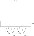
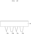
- FIGS. 9 and 10 illustrate shapes of protrusions of the electrode tab 110 according to various embodiments of the present disclosure.
- the protrusion of the electrode tab 110 may correspond to a welding protrusion 111.
- FIG. 8 illustrates protrusions 111 in case that the height of the protrusion 111 is formed smaller than the thickness of the electrode substrate 120 according to the prior art. If the height of the protrusion 111 is formed smaller than the thickness of the electrode substrate 120, the possibility of the protrusion 111 penetrating and damaging the electrode substrate 120 may decrease and the surface opposite the welding surface 113a and the surface opposite the bonding location 123' (refer to FIG. 7 ) can be formed substantially flat.
- FIG. 9 illustrates protrusions 111 in case that the lengths of protrusions are formed variously according to an embodiment of the present disclosure.
- the protrusion 111 may include a first protrusion set 111a having a first length and a second protrusion set 111b having a second length.
- the first protrusion set 111a or the second protrusion set 111b may include at least one protrusion.
- a bonding force can be adjusted by disposing protrusions 111 having different lengths and adjusting the depth of welding the electrode tab 110 and the electrode substrate 120.
- FIG. 10 illustrates protrusions 111 formed in various shapes according to an embodiment of the present disclosure.
- the protrusion 111 may include a third protrusion set 111c having a first shape and a fourth protrusion set 111d having a second shape.
- the protrusion having a first shape may be formed with a sharp end to increase a bonding depth with an electrode substrate.
- the protrusion 111 having a second shape may be formed with a flat end to increase a bonding area with an electrode substrate.
- the third protrusion set 111c and the fourth protrusion set 111d may include at least one protrusion.
- FIG. 11 illustrates one of protrusion shapes according to the prior art.
- protrusion 111 may be formed with a sharp end, flat end, angled end, or round end. Further, the whole shape of protrusion 111 may be formed in a funnel, diamond, rectangular column, rectangular horn, or cylinder shape.
- a bonding depth and a bonding area between an electrode tab and an electrode substrate can be adjusted and, accordingly, a bonding force between the electrode tab and the electrode substrate can be adjusted.
- FIG. 12 illustrates a battery packaged with an electrode assembly 100 and other members according to an embodiment of the present disclosure
- FIG. 13 illustrates an electronic device embedded with the packaged battery.
- the electrode assembly 100 may be used for an anode assembly 101 or a cathode assembly 103 (refer to FIG. 4 ) according to the active materials 125a and 125b deposited on a partial area of the electrode substrates 120a and 120b.
- an anode can be manufactured if a lithium-ion material, conductive material for improving a conductivity, and binder for improving a bonding force with the electrode substrate 120 are mixed and deposited
- a cathode can be manufactured if a conductive material, binder, and graphite are mixed and deposited.
- a membrane 200 may be located between an anode and a cathode, and a battery can be manufactured by winding and packing in a jelly roll shape as shown in FIG. 12 .
- an insulation film may be additionally disposed at a surface of the anode assembly 101 or the cathode assembly 103 according to the direction of winding the anode assembly 101, cathode assembly 103, and membrane 200.
- the surface opposite the bonding surface 113b and the surface opposite the bonding location 123' (refer to FIG. 7 ) of the electrode substrates 120a and 120b and the electrode tabs 110a and 110b are formed uniformly and smoothly, an influence of the surface opposite the bonding surface 113b and the surface opposite the bonding location 123' to other electrodes can be reduced in the process of winding and packing the electrode assembly.
- a battery according to an embodiment of the present disclosure may comprise an anode assembly 101, a cathode assembly 103, and a membrane disposed between the anode assembly and the cathode assembly.
- the anode assembly 101 or the cathode assembly 103 may comprise an electrode substrate, an active material 125 deposited in a first area 121 of the electrode substrate 120, and an electrode tab 110 attached in second area 123 of the electrode substrate where the active material 125 is not deposited.
- the bonding surface 113a of the electrode table 110 can comprise at least one protrusion 111 (refer to FIG. 5 ) formed, thereon contacting the bonding location of the second area of the electrode substrate 120, and a surface opposite the bonding surface 113b of the electrode tab 110 and a surface opposite the bonding location 123' may be substantially flat.
- the electrode assembly can be selected from one of a cathode assembly and an anode assembly.
- the battery further comprises the other of the cathode assembly and the anode assembly; and a membrane disposed between the electrode assembly and the other of the cathode assembly and the anode assembly.
- the electrode tab 110 may be fixed to the bonding location 123" by at least one protrusion 111.
- a surface of the electrode substrate 120 excluding the bonding location 123" may be substantially flat.
- the length of the at least one protrusion 111 (refer to FIG. 5 ) may be smaller than the thickness of the electrode substrate 120.
- the at least one protrusion 111 may comprise at least one first protrusion set 111a having a first length and at least one second protrusion set 111b having a second length (refer to FIG. 9 ).
- the at least one protrusion 111 may comprise at least one third protrusion set 111c having a first shape and at least one fourth protrusion set 111d having a second shape (refer to FIG. 10 ).
- the electrode tab 110 can be attached to the electrode substrate 120 by welding the at least one protrusion 111.
- a welding surface 113a (refer to FIG. 7 ) of the electrode tab 110 and the electrode substrate 120 may be formed in a part of a contacting area of the electrode tab 110 and the electrode substrate 120.
- An electronic device comprised according to an embodiment of the present disclosure may comprise a housing 1301, a display 1303 partially accommodated in the housing 1301, and a battery 1305 partially accommodated in the housing (refer to FIG. 13 ).
- the battery comprises an electrode assembly, the electrode assembly comprising an electrode substrate comprising a first area and a second area; an active material deposited on the first area of the electrode substrate; and an electrode tab attached to the second area of the electrode substrate, the electrode tab comprising a bonding surface having at least one protrusion contacting a bonding location of the second area of the electrode substrate, and wherein a surface opposite to the bonding surface of the electrode tab and a surface opposite to the bonding location are substantially flat.
- the electrode assembly can be selected from one of a cathode assembly and an anode assembly, wherein the battery further comprises the other of the cathode assembly and the anode assembly; and a membrane disposed between the electrode assembly and the other of the cathode assembly and the anode assembly.
- the electrode tab 110 can be fixed to the bonding location 123", preventing the membrane 200 (refer to FIG. 4 ) from being damaged by the at least one protrusion in a state of rolling up the battery.
- a surface of the electrode substrate 120 not contacting the electrode tab 110 may be substantially flat.
- the length of the at least one protrusion 111 (refer to FIG. 8 ) of the electronic tab 110 may be smaller than the thickness of the electrode substrate 120.
- the at least one protrusion 111 may comprise at least one first protrusion set 111a having a first length and at least one second protrusion set 111b having a second length (refer to FIG. 9 ).
- the at least one protrusion 111 may comprise at least one third protrusion set 111c having a first shape and at least one fourth protrusion set 111d having a second shape (refer to FIG. 10 ).
- the electrode tab 110 can be attached to the electrode substrate 120 by welding the at least one protrusion 111.
- a bonding surface 113a (refer to FIG. 7 ) of the electrode tab 110 can be formed in at least bonding location of the electrode tab 110 and the electrode substrate 120.
- FIG. 14 is a flowchart illustrating a procedure of manufacturing an electrode assembly according to an embodiment of the present disclosure.
- the electrode substrate can be manufactured through an operation 1401 of supplying an electrode substrate and an operation 1403 of depositing an active material to the supplied electrode substrate.
- the electrode tab can be manufactured through an operation of supplying an electrode tab sheet, an operation of cutting the supplied sheet according to a designed size of the electrode tab, and an operation 1409 of forming a welding protrusion on a welding surface of the electrode tab.
- the electrode tab sheet can be used by unwinding a roll at operation.
- the electrode tab sheet can be used by cutting into a predetermined size with a cutter at operation.
- the cut electrode tab 110 can be transported by an electrode tab transfer device 150 and processed for a welding protrusion 111 at operation 1409 by pressing with a jig 140 formed with protrusions.
- the welding part 113 of the electrode tab may mean a welding surface 113a of the electrode tab 110 and a non-welding surface 113b (refer to FIGS. 3 and 7 ).
- the operation 1401 of supplying an electrode substrate and the operation 1403 of depositing an active material on the electrode substrate can be performed after or at the same time as the operation of supplying an electrode tab sheet, the operation of cutting the supplied sheet according to a designed size of the electrode tab, and the operation 1409 of forming a welding protrusion on a welding surface of the electrode tab.
- the electrode tab 110 produced through the above procedure can be transported to an electrode substrate 120 with an electrode tab transfer device 150, and the electrode assembly can be manufactured by settling the electrode tab 110 on the electrode substrate 120 and welding the settled part at operation 1411.
- the surfaces of the horn 131 and the anvil 133 of the ultrasonic welding device 130 (refer to FIG. 5 ) used in an ultrasonic welding process may be formed in a practically flat shape corresponding to a contact with the electrode substrate 120 or the electrode tab 110.
- a non-welding surface 113b (refer to FIG. 7 ) can be formed uniformly and smoothly.
- a method for manufacturing a battery including an anode assembly 101, a cathode assembly 103, and a membrane 200 disposed between the anode assembly 101 and the cathode assembly 103 may comprise an operation 1401 of supplying an electrode substrate to be used for a pole assembly corresponding to the anode assembly 101 and the cathode assembly 103, an operation 1403 of depositing an active material 125 in a partial area of the electrode substrate, and an operation of attaching an electrode tab in another area of the electrode substrate.
- the operation of attaching an electrode tab may comprise an operation 1409 of forming at least one protrusion in at least one partial area of a second surface of the electrode tab opposite to a first area of the electrode tab having a practically flat shape, and an operation 1411 of combining the at least one protrusion with the electrode substrate in order to attach the at least one area of the second surface of the electrode tab to the electrode substrate.
- the operation 1409 of forming at least one protrusion may comprise an operation of pressing the electrode tab by using a jig formed with a protrusion.
- the operation 1411 of combining the at least one protrusion may comprise an operation of welding the at least one protrusion to the electrode substrate by using an ultrasonic wave.
- the operation of welding the at least one protrusion may comprise an operation of pressing the electrode tab onto the electrode substrate by using a horn or an anvil formed in a practically flat shape without having a concavo-convex or a protrusion.
- the combination of the electrode tab and the electrode substrate can be formed in at least one part of a contacting area between the electrode tab and the electrode substrate.
- the electrode assembly according to an embodiment of the present disclosure can be manufactured by forming a surface of a welding part uniformly and smoothly between an electrode substrate and an electrode tab.
Landscapes
- Chemical & Material Sciences (AREA)
- Chemical Kinetics & Catalysis (AREA)
- Electrochemistry (AREA)
- General Chemical & Material Sciences (AREA)
- Engineering & Computer Science (AREA)
- Manufacturing & Machinery (AREA)
- Microelectronics & Electronic Packaging (AREA)
- Materials Engineering (AREA)
- Connection Of Batteries Or Terminals (AREA)
Claims (14)
- Batterie (1305), umfassend:
eine Elektrodenanordnung (100), wobei die Elektrodenanordnung (100) umfasst:ein Elektrodensubstrat (120), umfassend einen ersten Bereich (121) und einem zweiten Bereich (123);ein aktives Material (125), das auf dem ersten Bereich (121) des Elektrodensubstrats (120) abgelagert ist; undeine Elektrodenlasche (110), die am zweiten Bereich (123) des Elektrodensubstrats (120) angebracht ist, wobei die Elektrodenlasche (110) eine Verbindungsfläche mit Vorsprüngen (111) umfasst, die Kontakt zu einer Verbindungsstelle des zweiten Bereichs (123) des Elektrodensubstrats (120) herstellen, wobei eine der Verbindungsfläche gegenüberliegende Fläche und eine der Verbindungsstelle gegenüberliegende Fläche im Wesentlichen flach sind;und dadurch gekennzeichnet,dass die Vorsprünge (111) einen ersten Satz Vorsprünge (111c), enthaltend eine Vielzahl von Vorsprüngen mit einer ersten Form, und einen zweiten Satz Vorsprünge (111d), enthaltend eine Vielzahl von Vorsprüngen mit einer zweiten Form, umfassen. - Batterie (1305) nach Anspruch 1, wobei die Vorsprünge (111) die Elektrodenlasche (110) an die Verbindungsstelle des zweiten Bereichs (123) des Elektrodensubstrats (120) befestigen.
- Batterie (1305) nach Anspruch 1, wobei eine Fläche des Elektrodensubstrats (120), mit Ausnahme der Verbindungsstelle des zweiten Bereichs (123), im Wesentlichen flach ist.
- Elektronische Vorrichtung, umfassend die Batterie (1305) nach Anspruch 1, wobei die elektronische Vorrichtung ferner umfasst:ein Gehäuse (1301); undeine Anzeige (1303), die teilweise im Gehäuse (1301) aufgenommen ist;wobei die Batterie (1305) teilweise im Gehäuse (1301) aufgenommen ist.
- Elektronische Vorrichtung nach Anspruch 4, wobei die Vorsprünge (111) die Elektrodenlasche (110) an die Verbindungsstelle des zweiten Bereichs (123) des Elektrodensubstrats (120) befestigen.
- Elektronische Vorrichtung nach Anspruch 4, wobei eine Fläche des Elektrodensubstrats (120), mit Ausnahme der Verbindungsstelle, im Wesentlichen flach ist.
- Elektronische Vorrichtung nach Anspruch 4, wobei die Länge der Vorsprünge (111) kleiner als die Dicke des Elektrodensubstrats (120) ist.
- Elektronische Vorrichtung nach Anspruch 4, wobei der Vorsprung (111) mindestens einen dritten Satz Vorsprünge (lila) mit einer ersten Länge und mindestens einen vierten Satz Vorsprünge (111b) mit einer zweiten Länge umfasst.
- Elektronische Vorrichtung nach Anspruch 4, wobei die Elektrodenlasche (110) an das Elektrodensubstrat (120) geschweißt ist.
- Elektronische Vorrichtung nach Anspruch 4, wobei eine Schweißfläche (113) zwischen der Elektrodenlasche (110) und dem Elektrodensubstrat (120) in einem Teil eines Kontaktbereichs zwischen der Elektrodenlasche (110) und dem Elektrodensubstrat (120) geformt ist.
- Verfahren zum Herstellen einer Batterie, umfassend eine Anodenanordnung, eine Kathodenanordnung und eine Membran (200), die zwischen der Anodenanordnung und der Kathodenanordnung angeordnet ist, wobei das Verfahren umfasst:ein Zuführen eines Elektrodensubstrats (120), das für eine Polanordnung entsprechend der Anodenanordnung und der Kathodenanordnung zu verwenden ist;ein Ablagern eines aktiven Materials (125) in einem Teilbereich des Elektrodensubstrats (120); undein Anbringen einer Elektrodenlasche (110) in einem anderen Bereich des Elektrodensubstrats (120), wobei das Anbringen einer Elektrodenlasche (110) umfasst:ein Formen von Vorsprüngen (111) in einer Verbindungsfläche der Elektrodenlasche (110) gegenüber einer im Wesentlichen flachen Fläche; undein Kombinieren der Vorsprünge (111) mit dem Elektrodensubstrat (120), um eine Verbindungsfläche der Elektrodenlasche (110) am Elektrodensubstrat (120) anzubringen;und dadurch gekennzeichnet, dassdie Vorsprünge (111) einen ersten Satz Vorsprünge (111c), enthaltend eine Vielzahl von Vorsprüngen mit einer ersten Form, und einen zweiten Satz Vorsprünge (111d), enthaltend eine Vielzahl von Vorsprüngen mit einer zweiten Form, umfassen.
- Verfahren nach Anspruch 11, wobei das Formen von Vorsprüngen (111) ein Drücken der Elektrodenlasche (110) mit einer mit einem Vorsprung (111) geformten Schablone (140) umfasst.
- Verfahren nach Anspruch 11, wobei das Kombinieren der Vorsprünge (111) ein Schweißen der Vorsprünge (111) an das Elektrodensubstrat (120) mithilfe einer Ultraschallwelle umfasst.
- Verfahren nach Anspruch 13, wobei das Schweißen der Vorsprünge (111) ein Drücken der Elektrodenlasche (110) auf das Elektrodensubstrat (120) mithilfe eines Horns (131) oder Ambosses (133), das bzw. der in einer im Wesentlichen flachen Form geformt ist, umfasst.
Applications Claiming Priority (1)
| Application Number | Priority Date | Filing Date | Title |
|---|---|---|---|
| KR1020170033381A KR102407054B1 (ko) | 2017-03-16 | 2017-03-16 | 평평한 일면을 갖는 전극 탭을 포함하는 배터리 |
Publications (2)
| Publication Number | Publication Date |
|---|---|
| EP3376565A1 EP3376565A1 (de) | 2018-09-19 |
| EP3376565B1 true EP3376565B1 (de) | 2019-12-25 |
Family
ID=61655672
Family Applications (1)
| Application Number | Title | Priority Date | Filing Date |
|---|---|---|---|
| EP18161791.1A Active EP3376565B1 (de) | 2017-03-16 | 2018-03-14 | Batterie mit elektrodenlasche mit flacher oberfläche |
Country Status (5)
| Country | Link |
|---|---|
| US (1) | US11050126B2 (de) |
| EP (1) | EP3376565B1 (de) |
| KR (1) | KR102407054B1 (de) |
| CN (1) | CN108630878B (de) |
| WO (1) | WO2018169271A1 (de) |
Families Citing this family (1)
| Publication number | Priority date | Publication date | Assignee | Title |
|---|---|---|---|---|
| KR20210114738A (ko) * | 2020-03-11 | 2021-09-24 | 주식회사 에보레이 | 피부질환 치료용 초소형 광 치료장치 |
Family Cites Families (20)
| Publication number | Priority date | Publication date | Assignee | Title |
|---|---|---|---|---|
| ZA986942B (en) | 1997-08-08 | 1999-02-08 | Duracell Inc | Reinforced coiled electrode assemblies and methods of producing same |
| JP3547959B2 (ja) * | 1997-11-21 | 2004-07-28 | 三洋電機株式会社 | リチウム電池及びその製造方法 |
| KR100890715B1 (ko) * | 2000-11-01 | 2009-03-27 | 소니 가부시끼 가이샤 | 전지, 전지의 제조 방법, 용접물의 제조 방법 및 페데스탈 |
| KR100601562B1 (ko) * | 2004-07-29 | 2006-07-19 | 삼성에스디아이 주식회사 | 전극 조립체 및 이를 이용한 리튬 이차 전지 |
| KR100601526B1 (ko) * | 2004-07-30 | 2006-07-19 | 삼성에스디아이 주식회사 | 리튬이온 이차전지 |
| JP5114950B2 (ja) * | 2006-02-13 | 2013-01-09 | 日産自動車株式会社 | 電池モジュール、組電池及びそれらの電池を搭載した車両 |
| KR100947982B1 (ko) * | 2006-03-28 | 2010-03-18 | 삼성에스디아이 주식회사 | 전극 조립체 및 이를 가지는 파우치형 리튬 이차 전지 |
| JP5063099B2 (ja) * | 2006-12-13 | 2012-10-31 | 三洋電機株式会社 | 太陽電池モジュール及び太陽電池モジュールの製造方法 |
| KR101101046B1 (ko) | 2009-12-01 | 2011-12-29 | 삼성에스디아이 주식회사 | 전극 조립체 및 그를 구비하는 이차 전지 |
| KR101473391B1 (ko) * | 2010-12-06 | 2014-12-16 | 주식회사 엘지화학 | 전극 조립체 및 이를 이용한 이차 전지 |
| CN102104134B (zh) * | 2011-01-28 | 2012-12-05 | 福建南平南孚电池有限公司 | 锂电池的极耳、具有该极耳的负极结构和锂电池 |
| KR101381674B1 (ko) | 2011-08-12 | 2014-04-04 | 주식회사 엘지화학 | 제조공정성이 향상된 젤리-롤 및 이를 포함하는 전지셀 |
| JP2014143230A (ja) * | 2013-01-22 | 2014-08-07 | Ibiden Co Ltd | 蓄電デバイス部品の製造方法、蓄電デバイスの製造方法、蓄電デバイス部品および蓄電デバイス。 |
| KR20140110353A (ko) * | 2013-03-07 | 2014-09-17 | 삼성에스디아이 주식회사 | 초음파 혼 및 이를 사용하여 제조된 이차 전지 |
| JP2014209525A (ja) * | 2013-03-26 | 2014-11-06 | ローム株式会社 | 電気キャパシタ、電気キャパシタモジュール、電気キャパシタの製造方法、および電気キャパシタモジュールの製造方法 |
| US9478829B2 (en) | 2013-05-16 | 2016-10-25 | Ec Power, Llc | Rechargeable battery with multiple resistance levels |
| KR102030110B1 (ko) | 2013-08-30 | 2019-11-08 | 삼성에스디아이 주식회사 | 이차 전지 |
| TWI646720B (zh) * | 2013-11-15 | 2019-01-01 | 日商半導體能源研究所股份有限公司 | 蓄電單元及電子裝置 |
| KR20160041645A (ko) * | 2014-10-08 | 2016-04-18 | 주식회사 엘지화학 | 2차 전지의 젤리롤형 전극 조립체 |
| KR102510882B1 (ko) * | 2015-07-16 | 2023-03-16 | 삼성에스디아이 주식회사 | 이차전지의 제조방법 |
-
2017
- 2017-03-16 KR KR1020170033381A patent/KR102407054B1/ko not_active Expired - Fee Related
-
2018
- 2018-03-13 WO PCT/KR2018/002908 patent/WO2018169271A1/en not_active Ceased
- 2018-03-14 EP EP18161791.1A patent/EP3376565B1/de active Active
- 2018-03-15 US US15/922,015 patent/US11050126B2/en not_active Expired - Fee Related
- 2018-03-16 CN CN201810217414.8A patent/CN108630878B/zh not_active Expired - Fee Related
Non-Patent Citations (1)
| Title |
|---|
| None * |
Also Published As
| Publication number | Publication date |
|---|---|
| KR20180105982A (ko) | 2018-10-01 |
| US20180269460A1 (en) | 2018-09-20 |
| CN108630878A (zh) | 2018-10-09 |
| EP3376565A1 (de) | 2018-09-19 |
| KR102407054B1 (ko) | 2022-06-10 |
| US11050126B2 (en) | 2021-06-29 |
| WO2018169271A1 (en) | 2018-09-20 |
| CN108630878B (zh) | 2022-09-20 |
Similar Documents
| Publication | Publication Date | Title |
|---|---|---|
| US11594752B2 (en) | Secondary battery and a method for fabricating the same | |
| CN103326028B (zh) | 蓄电装置及其制造方法 | |
| US8702818B2 (en) | Method of manufacturing an electrode assembly for a rechargeable battery | |
| US11043722B2 (en) | Flexible rechargeable battery | |
| CN105247726B (zh) | 弯曲的电极堆和包括该弯曲的电极堆的电池组 | |
| US9711763B2 (en) | Flexible secondary battery | |
| KR102520160B1 (ko) | 표면 실장 배터리 및 통합된 배터리 셀을 갖는 휴대용 전자 디바이스 | |
| KR102914039B1 (ko) | 배터리 및 이를 포함하는 전자 장치 | |
| US10873102B2 (en) | Methods and devices associated with bonding of solid-state lithium batteries | |
| CN103378337A (zh) | 蓄电装置以及其制造方法 | |
| JP2024120038A (ja) | 電極組立体、電池、及び電気機器 | |
| JP2005063958A (ja) | 薄膜固体リチウムイオン二次電池およびその製造方法 | |
| CN104350640A (zh) | 具有带的电极组件和包含所述电极组件的电化学装置 | |
| US10290892B2 (en) | Method of manufacturing rechargeable battery with curved surface | |
| JP5470335B2 (ja) | 捲回式二次電池 | |
| JP2015111566A (ja) | 電極部材、二次電池、及び電極部材の作製方法 | |
| EP3376565B1 (de) | Batterie mit elektrodenlasche mit flacher oberfläche | |
| US20040191622A1 (en) | Button type battery | |
| CN110114931B (zh) | 全固态电池的制造方法及其制造装置 | |
| KR20200142744A (ko) | 배터리 스택 및 그 제조방법 | |
| US7927746B2 (en) | Systems and methods for internal short circuit protection in battery cells | |
| KR20180037840A (ko) | 이차 전지 | |
| EP3309871A1 (de) | Elektrodenanordnung, lithium-ionen-batterie und elektronische vorrichtung damit | |
| KR20220104782A (ko) | 비수 전해질 이차 전지, 집전체, 및 이들의 제조 방법 | |
| JP2002198019A (ja) | 非水電解質電池およびその製造方法 |
Legal Events
| Date | Code | Title | Description |
|---|---|---|---|
| PUAI | Public reference made under article 153(3) epc to a published international application that has entered the european phase |
Free format text: ORIGINAL CODE: 0009012 |
|
| STAA | Information on the status of an ep patent application or granted ep patent |
Free format text: STATUS: THE APPLICATION HAS BEEN PUBLISHED |
|
| AK | Designated contracting states |
Kind code of ref document: A1 Designated state(s): AL AT BE BG CH CY CZ DE DK EE ES FI FR GB GR HR HU IE IS IT LI LT LU LV MC MK MT NL NO PL PT RO RS SE SI SK SM TR |
|
| AX | Request for extension of the european patent |
Extension state: BA ME |
|
| STAA | Information on the status of an ep patent application or granted ep patent |
Free format text: STATUS: REQUEST FOR EXAMINATION WAS MADE |
|
| 17P | Request for examination filed |
Effective date: 20181004 |
|
| RBV | Designated contracting states (corrected) |
Designated state(s): AL AT BE BG CH CY CZ DE DK EE ES FI FR GB GR HR HU IE IS IT LI LT LU LV MC MK MT NL NO PL PT RO RS SE SI SK SM TR |
|
| GRAJ | Information related to disapproval of communication of intention to grant by the applicant or resumption of examination proceedings by the epo deleted |
Free format text: ORIGINAL CODE: EPIDOSDIGR1 |
|
| STAA | Information on the status of an ep patent application or granted ep patent |
Free format text: STATUS: GRANT OF PATENT IS INTENDED |
|
| RIC1 | Information provided on ipc code assigned before grant |
Ipc: H01M 10/04 20060101ALI20190611BHEP Ipc: H01M 2/26 20060101ALI20190611BHEP Ipc: H05K 5/00 20060101ALI20190611BHEP Ipc: H01M 4/139 20100101ALI20190611BHEP Ipc: H01M 10/0587 20100101ALN20190611BHEP Ipc: H01M 2/30 20060101ALI20190611BHEP Ipc: H01M 2/22 20060101AFI20190611BHEP |
|
| GRAP | Despatch of communication of intention to grant a patent |
Free format text: ORIGINAL CODE: EPIDOSNIGR1 |
|
| INTG | Intention to grant announced |
Effective date: 20190719 |
|
| GRAS | Grant fee paid |
Free format text: ORIGINAL CODE: EPIDOSNIGR3 |
|
| GRAA | (expected) grant |
Free format text: ORIGINAL CODE: 0009210 |
|
| STAA | Information on the status of an ep patent application or granted ep patent |
Free format text: STATUS: THE PATENT HAS BEEN GRANTED |
|
| AK | Designated contracting states |
Kind code of ref document: B1 Designated state(s): AL AT BE BG CH CY CZ DE DK EE ES FI FR GB GR HR HU IE IS IT LI LT LU LV MC MK MT NL NO PL PT RO RS SE SI SK SM TR |
|
| REG | Reference to a national code |
Ref country code: GB Ref legal event code: FG4D |
|
| REG | Reference to a national code |
Ref country code: CH Ref legal event code: EP |
|
| REG | Reference to a national code |
Ref country code: AT Ref legal event code: REF Ref document number: 1218118 Country of ref document: AT Kind code of ref document: T Effective date: 20200115 |
|
| REG | Reference to a national code |
Ref country code: DE Ref legal event code: R096 Ref document number: 602018001721 Country of ref document: DE |
|
| REG | Reference to a national code |
Ref country code: IE Ref legal event code: FG4D |
|
| PG25 | Lapsed in a contracting state [announced via postgrant information from national office to epo] |
Ref country code: LT Free format text: LAPSE BECAUSE OF FAILURE TO SUBMIT A TRANSLATION OF THE DESCRIPTION OR TO PAY THE FEE WITHIN THE PRESCRIBED TIME-LIMIT Effective date: 20191225 Ref country code: NO Free format text: LAPSE BECAUSE OF FAILURE TO SUBMIT A TRANSLATION OF THE DESCRIPTION OR TO PAY THE FEE WITHIN THE PRESCRIBED TIME-LIMIT Effective date: 20200325 Ref country code: SE Free format text: LAPSE BECAUSE OF FAILURE TO SUBMIT A TRANSLATION OF THE DESCRIPTION OR TO PAY THE FEE WITHIN THE PRESCRIBED TIME-LIMIT Effective date: 20191225 Ref country code: LV Free format text: LAPSE BECAUSE OF FAILURE TO SUBMIT A TRANSLATION OF THE DESCRIPTION OR TO PAY THE FEE WITHIN THE PRESCRIBED TIME-LIMIT Effective date: 20191225 Ref country code: GR Free format text: LAPSE BECAUSE OF FAILURE TO SUBMIT A TRANSLATION OF THE DESCRIPTION OR TO PAY THE FEE WITHIN THE PRESCRIBED TIME-LIMIT Effective date: 20200326 Ref country code: FI Free format text: LAPSE BECAUSE OF FAILURE TO SUBMIT A TRANSLATION OF THE DESCRIPTION OR TO PAY THE FEE WITHIN THE PRESCRIBED TIME-LIMIT Effective date: 20191225 Ref country code: BG Free format text: LAPSE BECAUSE OF FAILURE TO SUBMIT A TRANSLATION OF THE DESCRIPTION OR TO PAY THE FEE WITHIN THE PRESCRIBED TIME-LIMIT Effective date: 20200325 |
|
| REG | Reference to a national code |
Ref country code: NL Ref legal event code: FP |
|
| REG | Reference to a national code |
Ref country code: LT Ref legal event code: MG4D |
|
| PG25 | Lapsed in a contracting state [announced via postgrant information from national office to epo] |
Ref country code: RS Free format text: LAPSE BECAUSE OF FAILURE TO SUBMIT A TRANSLATION OF THE DESCRIPTION OR TO PAY THE FEE WITHIN THE PRESCRIBED TIME-LIMIT Effective date: 20191225 Ref country code: HR Free format text: LAPSE BECAUSE OF FAILURE TO SUBMIT A TRANSLATION OF THE DESCRIPTION OR TO PAY THE FEE WITHIN THE PRESCRIBED TIME-LIMIT Effective date: 20191225 |
|
| PG25 | Lapsed in a contracting state [announced via postgrant information from national office to epo] |
Ref country code: AL Free format text: LAPSE BECAUSE OF FAILURE TO SUBMIT A TRANSLATION OF THE DESCRIPTION OR TO PAY THE FEE WITHIN THE PRESCRIBED TIME-LIMIT Effective date: 20191225 |
|
| PG25 | Lapsed in a contracting state [announced via postgrant information from national office to epo] |
Ref country code: EE Free format text: LAPSE BECAUSE OF FAILURE TO SUBMIT A TRANSLATION OF THE DESCRIPTION OR TO PAY THE FEE WITHIN THE PRESCRIBED TIME-LIMIT Effective date: 20191225 Ref country code: RO Free format text: LAPSE BECAUSE OF FAILURE TO SUBMIT A TRANSLATION OF THE DESCRIPTION OR TO PAY THE FEE WITHIN THE PRESCRIBED TIME-LIMIT Effective date: 20191225 Ref country code: PT Free format text: LAPSE BECAUSE OF FAILURE TO SUBMIT A TRANSLATION OF THE DESCRIPTION OR TO PAY THE FEE WITHIN THE PRESCRIBED TIME-LIMIT Effective date: 20200520 Ref country code: CZ Free format text: LAPSE BECAUSE OF FAILURE TO SUBMIT A TRANSLATION OF THE DESCRIPTION OR TO PAY THE FEE WITHIN THE PRESCRIBED TIME-LIMIT Effective date: 20191225 |
|
| PG25 | Lapsed in a contracting state [announced via postgrant information from national office to epo] |
Ref country code: IS Free format text: LAPSE BECAUSE OF FAILURE TO SUBMIT A TRANSLATION OF THE DESCRIPTION OR TO PAY THE FEE WITHIN THE PRESCRIBED TIME-LIMIT Effective date: 20200425 Ref country code: SK Free format text: LAPSE BECAUSE OF FAILURE TO SUBMIT A TRANSLATION OF THE DESCRIPTION OR TO PAY THE FEE WITHIN THE PRESCRIBED TIME-LIMIT Effective date: 20191225 Ref country code: SM Free format text: LAPSE BECAUSE OF FAILURE TO SUBMIT A TRANSLATION OF THE DESCRIPTION OR TO PAY THE FEE WITHIN THE PRESCRIBED TIME-LIMIT Effective date: 20191225 |
|
| REG | Reference to a national code |
Ref country code: DE Ref legal event code: R097 Ref document number: 602018001721 Country of ref document: DE |
|
| PG25 | Lapsed in a contracting state [announced via postgrant information from national office to epo] |
Ref country code: DK Free format text: LAPSE BECAUSE OF FAILURE TO SUBMIT A TRANSLATION OF THE DESCRIPTION OR TO PAY THE FEE WITHIN THE PRESCRIBED TIME-LIMIT Effective date: 20191225 Ref country code: ES Free format text: LAPSE BECAUSE OF FAILURE TO SUBMIT A TRANSLATION OF THE DESCRIPTION OR TO PAY THE FEE WITHIN THE PRESCRIBED TIME-LIMIT Effective date: 20191225 Ref country code: MC Free format text: LAPSE BECAUSE OF FAILURE TO SUBMIT A TRANSLATION OF THE DESCRIPTION OR TO PAY THE FEE WITHIN THE PRESCRIBED TIME-LIMIT Effective date: 20191225 |
|
| PLBE | No opposition filed within time limit |
Free format text: ORIGINAL CODE: 0009261 |
|
| STAA | Information on the status of an ep patent application or granted ep patent |
Free format text: STATUS: NO OPPOSITION FILED WITHIN TIME LIMIT |
|
| REG | Reference to a national code |
Ref country code: AT Ref legal event code: MK05 Ref document number: 1218118 Country of ref document: AT Kind code of ref document: T Effective date: 20191225 |
|
| REG | Reference to a national code |
Ref country code: DE Ref legal event code: R079 Ref document number: 602018001721 Country of ref document: DE Free format text: PREVIOUS MAIN CLASS: H01M0002220000 Ipc: H01M0050528000 |
|
| PG25 | Lapsed in a contracting state [announced via postgrant information from national office to epo] |
Ref country code: SI Free format text: LAPSE BECAUSE OF FAILURE TO SUBMIT A TRANSLATION OF THE DESCRIPTION OR TO PAY THE FEE WITHIN THE PRESCRIBED TIME-LIMIT Effective date: 20191225 |
|
| 26N | No opposition filed |
Effective date: 20200928 |
|
| REG | Reference to a national code |
Ref country code: BE Ref legal event code: MM Effective date: 20200331 |
|
| PG25 | Lapsed in a contracting state [announced via postgrant information from national office to epo] |
Ref country code: LU Free format text: LAPSE BECAUSE OF NON-PAYMENT OF DUE FEES Effective date: 20200314 |
|
| PG25 | Lapsed in a contracting state [announced via postgrant information from national office to epo] |
Ref country code: IT Free format text: LAPSE BECAUSE OF FAILURE TO SUBMIT A TRANSLATION OF THE DESCRIPTION OR TO PAY THE FEE WITHIN THE PRESCRIBED TIME-LIMIT Effective date: 20191225 Ref country code: IE Free format text: LAPSE BECAUSE OF NON-PAYMENT OF DUE FEES Effective date: 20200314 Ref country code: FR Free format text: LAPSE BECAUSE OF NON-PAYMENT OF DUE FEES Effective date: 20200331 Ref country code: AT Free format text: LAPSE BECAUSE OF FAILURE TO SUBMIT A TRANSLATION OF THE DESCRIPTION OR TO PAY THE FEE WITHIN THE PRESCRIBED TIME-LIMIT Effective date: 20191225 |
|
| PG25 | Lapsed in a contracting state [announced via postgrant information from national office to epo] |
Ref country code: PL Free format text: LAPSE BECAUSE OF FAILURE TO SUBMIT A TRANSLATION OF THE DESCRIPTION OR TO PAY THE FEE WITHIN THE PRESCRIBED TIME-LIMIT Effective date: 20191225 Ref country code: BE Free format text: LAPSE BECAUSE OF NON-PAYMENT OF DUE FEES Effective date: 20200331 |
|
| REG | Reference to a national code |
Ref country code: CH Ref legal event code: PL |
|
| PG25 | Lapsed in a contracting state [announced via postgrant information from national office to epo] |
Ref country code: CH Free format text: LAPSE BECAUSE OF NON-PAYMENT OF DUE FEES Effective date: 20210331 Ref country code: LI Free format text: LAPSE BECAUSE OF NON-PAYMENT OF DUE FEES Effective date: 20210331 |
|
| PGFP | Annual fee paid to national office [announced via postgrant information from national office to epo] |
Ref country code: GB Payment date: 20220221 Year of fee payment: 5 |
|
| PG25 | Lapsed in a contracting state [announced via postgrant information from national office to epo] |
Ref country code: TR Free format text: LAPSE BECAUSE OF FAILURE TO SUBMIT A TRANSLATION OF THE DESCRIPTION OR TO PAY THE FEE WITHIN THE PRESCRIBED TIME-LIMIT Effective date: 20191225 Ref country code: MT Free format text: LAPSE BECAUSE OF FAILURE TO SUBMIT A TRANSLATION OF THE DESCRIPTION OR TO PAY THE FEE WITHIN THE PRESCRIBED TIME-LIMIT Effective date: 20191225 Ref country code: CY Free format text: LAPSE BECAUSE OF FAILURE TO SUBMIT A TRANSLATION OF THE DESCRIPTION OR TO PAY THE FEE WITHIN THE PRESCRIBED TIME-LIMIT Effective date: 20191225 |
|
| PGFP | Annual fee paid to national office [announced via postgrant information from national office to epo] |
Ref country code: NL Payment date: 20220222 Year of fee payment: 5 |
|
| PG25 | Lapsed in a contracting state [announced via postgrant information from national office to epo] |
Ref country code: MK Free format text: LAPSE BECAUSE OF FAILURE TO SUBMIT A TRANSLATION OF THE DESCRIPTION OR TO PAY THE FEE WITHIN THE PRESCRIBED TIME-LIMIT Effective date: 20191225 |
|
| PGFP | Annual fee paid to national office [announced via postgrant information from national office to epo] |
Ref country code: DE Payment date: 20230220 Year of fee payment: 6 |
|
| REG | Reference to a national code |
Ref country code: NL Ref legal event code: MM Effective date: 20230401 |
|
| GBPC | Gb: european patent ceased through non-payment of renewal fee |
Effective date: 20230314 |
|
| PG25 | Lapsed in a contracting state [announced via postgrant information from national office to epo] |
Ref country code: NL Free format text: LAPSE BECAUSE OF NON-PAYMENT OF DUE FEES Effective date: 20230401 |
|
| PG25 | Lapsed in a contracting state [announced via postgrant information from national office to epo] |
Ref country code: GB Free format text: LAPSE BECAUSE OF NON-PAYMENT OF DUE FEES Effective date: 20230314 |
|
| PG25 | Lapsed in a contracting state [announced via postgrant information from national office to epo] |
Ref country code: GB Free format text: LAPSE BECAUSE OF NON-PAYMENT OF DUE FEES Effective date: 20230314 |
|
| REG | Reference to a national code |
Ref country code: DE Ref legal event code: R119 Ref document number: 602018001721 Country of ref document: DE |
|
| PG25 | Lapsed in a contracting state [announced via postgrant information from national office to epo] |
Ref country code: DE Free format text: LAPSE BECAUSE OF NON-PAYMENT OF DUE FEES Effective date: 20241001 |
|
| PG25 | Lapsed in a contracting state [announced via postgrant information from national office to epo] |
Ref country code: DE Free format text: LAPSE BECAUSE OF NON-PAYMENT OF DUE FEES Effective date: 20241001 |