EP3376532B1 - Procédé de fabrication d'une puce - Google Patents
Procédé de fabrication d'une puce Download PDFInfo
- Publication number
- EP3376532B1 EP3376532B1 EP17196040.4A EP17196040A EP3376532B1 EP 3376532 B1 EP3376532 B1 EP 3376532B1 EP 17196040 A EP17196040 A EP 17196040A EP 3376532 B1 EP3376532 B1 EP 3376532B1
- Authority
- EP
- European Patent Office
- Prior art keywords
- chip
- region
- chips
- circuit unit
- manufacturing
- Prior art date
- Legal status (The legal status is an assumption and is not a legal conclusion. Google has not performed a legal analysis and makes no representation as to the accuracy of the status listed.)
- Active
Links
Images



Classifications
-
- H—ELECTRICITY
- H10—SEMICONDUCTOR DEVICES; ELECTRIC SOLID-STATE DEVICES NOT OTHERWISE PROVIDED FOR
- H10D—INORGANIC ELECTRIC SEMICONDUCTOR DEVICES
- H10D89/00—Aspects of integrated devices not covered by groups H10D84/00 - H10D88/00
- H10D89/10—Integrated device layouts
-
- C—CHEMISTRY; METALLURGY
- C30—CRYSTAL GROWTH
- C30B—SINGLE-CRYSTAL GROWTH; UNIDIRECTIONAL SOLIDIFICATION OF EUTECTIC MATERIAL OR UNIDIRECTIONAL DEMIXING OF EUTECTOID MATERIAL; REFINING BY ZONE-MELTING OF MATERIAL; PRODUCTION OF A HOMOGENEOUS POLYCRYSTALLINE MATERIAL WITH DEFINED STRUCTURE; SINGLE CRYSTALS OR HOMOGENEOUS POLYCRYSTALLINE MATERIAL WITH DEFINED STRUCTURE; AFTER-TREATMENT OF SINGLE CRYSTALS OR A HOMOGENEOUS POLYCRYSTALLINE MATERIAL WITH DEFINED STRUCTURE; APPARATUS THEREFOR
- C30B15/00—Single-crystal growth by pulling from a melt, e.g. Czochralski method
-
- C—CHEMISTRY; METALLURGY
- C30—CRYSTAL GROWTH
- C30B—SINGLE-CRYSTAL GROWTH; UNIDIRECTIONAL SOLIDIFICATION OF EUTECTIC MATERIAL OR UNIDIRECTIONAL DEMIXING OF EUTECTOID MATERIAL; REFINING BY ZONE-MELTING OF MATERIAL; PRODUCTION OF A HOMOGENEOUS POLYCRYSTALLINE MATERIAL WITH DEFINED STRUCTURE; SINGLE CRYSTALS OR HOMOGENEOUS POLYCRYSTALLINE MATERIAL WITH DEFINED STRUCTURE; AFTER-TREATMENT OF SINGLE CRYSTALS OR A HOMOGENEOUS POLYCRYSTALLINE MATERIAL WITH DEFINED STRUCTURE; APPARATUS THEREFOR
- C30B29/00—Single crystals or homogeneous polycrystalline material with defined structure characterised by the material or by their shape
- C30B29/02—Elements
- C30B29/06—Silicon
-
- G—PHYSICS
- G06—COMPUTING OR CALCULATING; COUNTING
- G06F—ELECTRIC DIGITAL DATA PROCESSING
- G06F30/00—Computer-aided design [CAD]
- G06F30/30—Circuit design
- G06F30/39—Circuit design at the physical level
- G06F30/392—Floor-planning or layout, e.g. partitioning or placement
-
- H—ELECTRICITY
- H10—SEMICONDUCTOR DEVICES; ELECTRIC SOLID-STATE DEVICES NOT OTHERWISE PROVIDED FOR
- H10D—INORGANIC ELECTRIC SEMICONDUCTOR DEVICES
- H10D84/00—Integrated devices formed in or on semiconductor substrates that comprise only semiconducting layers, e.g. on Si wafers or on GaAs-on-Si wafers
- H10D84/01—Manufacture or treatment
-
- H—ELECTRICITY
- H10—SEMICONDUCTOR DEVICES; ELECTRIC SOLID-STATE DEVICES NOT OTHERWISE PROVIDED FOR
- H10D—INORGANIC ELECTRIC SEMICONDUCTOR DEVICES
- H10D84/00—Integrated devices formed in or on semiconductor substrates that comprise only semiconducting layers, e.g. on Si wafers or on GaAs-on-Si wafers
- H10D84/01—Manufacture or treatment
- H10D84/02—Manufacture or treatment characterised by using material-based technologies
- H10D84/03—Manufacture or treatment characterised by using material-based technologies using Group IV technology, e.g. silicon technology or silicon-carbide [SiC] technology
- H10D84/038—Manufacture or treatment characterised by using material-based technologies using Group IV technology, e.g. silicon technology or silicon-carbide [SiC] technology using silicon technology, e.g. SiGe
-
- H—ELECTRICITY
- H10—SEMICONDUCTOR DEVICES; ELECTRIC SOLID-STATE DEVICES NOT OTHERWISE PROVIDED FOR
- H10P—GENERIC PROCESSES OR APPARATUS FOR THE MANUFACTURE OR TREATMENT OF DEVICES COVERED BY CLASS H10
- H10P54/00—Cutting or separating of wafers, substrates or parts of devices
Definitions
- the present disclosure relates to a technical field of mobile terminals, and more particularly to a chip, a manufacturing method, and a mobile terminal.
- Related technologies are known from US 6 078 096 A and US 5 801 406 A .
- US 2004/245618 A1 discloses a method of forming a plurality of chips with subsequent cutting, wherein the chips include a first chip and a second chip, wherein the first chip and the second chip differ only in circuits at the edge of the chips.
- chip-manufacturing methods include following operations. Chips are processed according to highest specification to obtain high-specification chips. To form lower specification chips, part of functional units of the high-specification chips is disabled by melting fuses thereof or other methods, or main operation frequencies of the high-specification chips are lowered.
- a core size or a die size of the lower specification chip is identical to a core size or a die size of the high-specification chip.
- the die size of the high-specification chip is 10mm ⁇ 10mm and the die size of the lower specification chip is also the same. Therefore, the conventional method of manufacturing the lower specification chip is apparently disadvantageous regarding the reduction of the cost.
- Embodiments of the present disclosure provide a manufacturing method, so that the cost of the lower specification chip can be reduced, and configuration efficiency of the chips having different specifications can be improved.
- the present disclosure provides a method of manufacturing a chip that includes following actions.
- a chip substrate is divided into a plurality of chip regions.
- a first region of each of the chip regions is processed, for forming at least one first circuit unit set.
- a second region of each of the chip regions is process, for forming a second circuit unit set.
- the at least one first circuit unit set includes a plurality of same circuit units.
- a size of the first region of the chip is determined by a number of the circuit units in the first region. The number of the circuit units in the first region determines a specification of the chip.
- the chip substrate is cut for forming a plurality of chips.
- a specification of the chip and size of the first region are determined by the number of the circuit units in the first region.
- the number of the circuit units in the first region determines a specification of the chip.
- size of the lower specification chip is relatively less than size of the high-specification chip, so that the number of lower specification chips which is produced by a same chip substrate can be increased relatively, and the cost of single lower specification chip can be correspondingly reduced to decrease the chip cost.
- the lower specification chip is formed by physically adjusting the number of the circuit units in the first region for reducing specification level of chips, there is no need to form the lower specification chip by reducing performance of the high-specification chip using a fuse-melted manner, so that configuration efficiency of the chips having different specifications can be improved.
- first and second are used only for purposes of description, and cannot be understood to indicate or imply a relative importance or to implicitly indicate the number of technical features indicated.
- the features “first” and “second” can be expressly or implicitly included in one or more of the features.
- the meanings of “multiple” are two or more, unless specifically limited otherwise.
- FIG. 1 is an illustrative structural diagram of a chip 100 manufactured according to the present disclosure.
- the chip 100 includes a first region 110 and a second region 120.
- the first region 110 is formed by at least one first circuit unit set 110a.
- the second region 120 is formed by a second circuit unit set 120a.
- the at least one first circuit unit set 110a includes identical circuit units 10.
- a number of the circuit units 110 in the first region 110 determines a specification of the chip 100 and a size of the first region 110.
- the specification of the chip includes a number of logic circuits of the chip.
- the number of the logic circuits of a high-specification chip is greater than the number of the logic circuits of a lower specification chip.
- the specification of the chip includes an operational frequency of the chip.
- the operational frequency of the high-specification chip is greater than the operational frequency of the lower specification chip.
- the second circuit unit set 120a includes at least one circuit unit 10.
- the at least one circuit unit 10 of the second circuit unit set 120a is the same as circuit units 10 in the at least one first circuit unit set 110a.
- the at least one circuit unit 10 of the second circuit unit set 120a can be also different from the circuit units 10 in the at least one first circuit unit set 110a.
- second circuit unit sets 120a in different specification chips are the same each other.
- a specification of the chip and size of the first region 110 are determined by the number of the circuit units 10 in the first region 110.
- the sizes of the chips in various types of specifications are correspondingly different, so that the size of lower specification chip and the number of the circuit units 10 in the first region 110 are relatively small, and the cost of the lower specification chip can be reduced.
- the lower specification chip is formed by physically adjusting the number of the circuit units 10 in the first region 110 for reducing specification level of chips, there is no need to form the lower specification chip by reducing performance of the high-specification chip using a fuse-melted manner, so that configuration efficiency of the chips having different specifications can be improved.
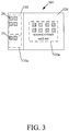
- the chip is a first chip 200 or a second chip 300.
- the specification of the first chip 200 is better than the specification of the second chip 300.
- the size of the first region 210 of the first chip 200 is greater than size of the first region 310 of the second chip 300.
- the first chip 200 has at least one more circuit unit 20 (e.g., three circuit units in FIG. 2 ) than the second chip 300.
- the at least one circuit unit 20 is arranged in a side region 211 of the first region 210, and except the side region 211, an area of an region of the first chip 200 is the same as an area of an region of the second chip 300.
- the first chip 200 is the same as the second chip 300 except the side region 211.
- the difference between the first chip 200 and the second chip 300 is the at least one circuit unit 20 in the side region 211.
- the second chip 300 can be regarded as part of the first chip 200.
- the side region 211 is easily distinguished from the first chip 200.
- the second chip 300 can be formed by only directly cutting the side region 211 of the first chip 200, so that the cost expenditure of the second chip 300 in the development and manufacturing stages is greatly reduced.
- the manufacturing methods of the first chip 200 and the second chip 300 can reduce the cost and improve the competitiveness of products.
- the circuit units include a plurality of analog circuits or digital circuits.
- each of the circuit units is selected from the group consisting of transistors, resistors, capacitors, inductors, and metal wirings.
- the transistors can be, for example, a diode, a triode, a field-effect transistor and the like.
- the number of components, such as transistors, resistors, capacitors, inductors, and metal wirings, in the circuit units of the present disclosure is not limited.
- a shape of the chip 100 is selected from the group consisting of a square shape, a rectangular shape, a circular shape, and an oval shape.
- size of the chip 100 is can be 10 square millimeters, 100 square millimeters or the like.
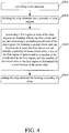
- FIG. 4 is an illustrative flowchart of a method of manufacturing the chip 100 according to one embodiment of the present disclosure.
- the method of manufacturing the chip 100 includes following action blocks.
- a chip substrate is provided.
- the chip substrate is divided into a plurality of chip regions.
- a first region of each of the chip regions is processed for forming at least one first circuit unit set.
- a second region of each of the chip regions is processed for forming a second circuit unit set.
- the at least one first circuit unit set includes a plurality of same circuit units.
- a size of the first region is determined by a number of the circuit units in the first region. The number of the circuit units in the first region determines a specification of the chip.
- the chip substrate is cut to form a plurality of chips.
- a specification of the chip 100 and size of the first region 110 are determined by the number of the circuit units in the first region 110.
- the number of the circuit units in the first region 110 determines a specification of the chip 100.
- size of the lower specification chip is relatively less than size of the high-specification chip, so that the number of lower specification chips which is produced by a same chip substrate can be increased relatively, and the cost of single lower specification chip can be correspondingly reduced to decrease the chip cost.
- the lower specification chip is formed by physically adjusting the number of the circuit units in the first region 110 for reducing specification level of chips, there is no need to form the lower specification chip by reducing performance of the high-specification chip using a fuse-melted manner, so that configuration efficiency of the chips having different specifications can be improved.
- a 12-inch chip substrate is fixed at the total price.
- larger number of chips produced by the chip substrate means that the cost of single chip is reduced.
- the number of chips which can be produced by the chip substrate is determined by the chip size (e.g., a core size or a die size).
- the die size of the chip A is 100 square millimeters, so that 660 chips A can be produced by the 12-inch chip substrate.
- the die size of the chip B is 10 square millimeters, so that number of 6600 chips B can be produced by the 12-inch chip substrate.
- the production cost difference between the chip A and the chip B is 10 multiples.
- the chip is a first chip 200 or a second chip 300.
- the specification of the first chip 200 is better than the specification of the second chip 300.
- the size of the first region 210 of the first chip 200 is greater than the size of the first region 310 of the second chip 300.
- the first chip 200 has at least one more circuit unit 20 (e.g., three circuit units in FIG. 2 ) than the second chip 300.
- the at least one circuit unit 20 is arranged in a side region 211 of the first region 210, and except the side region 211, an area of an region of the first chip 200 is the same as an area of an region of the second chip 300.
- the first chip 200 is the same as the second chip 300 except the side region 211.
- the first region 210 is formed by at least one first circuit unit set 210a.
- the second region 220 is formed by a second circuit unit set 220a.
- the first region 310 is formed by at least one first circuit unit set 310a.
- the second region 320 is formed by a second circuit unit set 320a.
- the difference between the first chip 200 and the second chip 300 is the at least one circuit unit 20 in the side region 211.
- the second chip 300 can be regarded as part of the first chip 200.
- the side region 211 is easily distinguished from the first chip 200.
- the second chip 300 can be formed by only directly cutting the side region 211 of the first chip 200, so that the cost expenditure of the second chip 300 in the development and manufacturing stages is greatly reduced.
- the manufacturing methods of the first chip 200 and the second chip 300 can reduce the cost and improve the competitiveness of products.
- the circuit units 20 include a plurality of analog circuits or digital circuits.
- each of the circuit units is selected from the group consisting of transistors, resistors, capacitors, inductors, and metal wirings.
- the transistors can be, for example, a diode, a triode, a field-effect transistor and the like.
- the number of components, such as transistors, resistors, capacitors, inductors, and metal wirings, in the circuit units of the present disclosure is not limited.
- a shape of the chip 100 is selected from the group consisting of a square shape, a rectangular shape, a circular shape, and an oval shape.
- size of the chip 100 is can be 10 square millimeters, 100 square millimeters or the like.
- the chip substrate is a wafer.
- providing the chip substrate further includes following actions.
- the silicon material is melted for forming liquid silicon.
- the liquid silicon is injected into a quartz container.
- the liquid silicon is rotated and stretched for forming a cylindrical silicon ingot.
- the cylindrical silicon ingot is sliced, to obtain a silicon ingot slice.
- the substance atoms are added into the silicon ingot slice for forming the chip substrate.
- a coating operation, an exposure operation, a developing operation, an etching operation, a particle implantation operation, and a metal sputtering operation are performed, for forming the at least one first circuit unit set.
- FIG. 5 is an illustrative structural diagram of a mobile terminal 500
- the mobile terminal 500 includes at least one chip, as shown illustrated in FIG. 1 to FIG. 3 .
- the at least one chip includes different components, such as at least one processor and memory, that are arranged in the mobile terminal 500.
- a smart phone having multiple cores are installed with the at least one processor, so that different configuration specifications of chips are achieved.
- the mobile terminal 500 can be a mobile phone, a tablet computer, a notebook computer and the like.
- the actions of the method disclosed by the embodiments of present disclosure can be embodied directly as a hardware decoding processor can be directly executed by a hardware decoding processor, or by combinations of hardware and software codes in a decoding processor.
- the software codes can be stored in a storage medium selected from one group consisting of random access memory, a flash memory, a read-only memory, a programmable read-only memory, an electrically erasable programmable memory, and registers.
- the processor read information (e.g., instructions) in the memory and completes the above-mentioned actions of the method in combination with hardware.
Landscapes
- Engineering & Computer Science (AREA)
- Chemical & Material Sciences (AREA)
- Theoretical Computer Science (AREA)
- Computer Hardware Design (AREA)
- Physics & Mathematics (AREA)
- Metallurgy (AREA)
- Crystallography & Structural Chemistry (AREA)
- Materials Engineering (AREA)
- Organic Chemistry (AREA)
- General Engineering & Computer Science (AREA)
- General Physics & Mathematics (AREA)
- Geometry (AREA)
- Evolutionary Computation (AREA)
- Architecture (AREA)
- Semiconductor Integrated Circuits (AREA)
- Design And Manufacture Of Integrated Circuits (AREA)
Claims (7)
- Procédé de fabrication d'une pluralité de puces (100), comprenant :la division d'un substrat de puce en une pluralité de régions de puce ;le traitement d'une première région (110) de chacune des régions de puce pour former au moins un premier ensemble d'unités de circuit (110a) ;le traitement d'une seconde région (120) de chacune des régions de puce pour former un second ensemble d'unités de circuit (120a),l'au moins un premier ensemble d'unités de circuit (110a) comprenant une pluralité d'unités de circuit identiques (10),une taille de la première région (110) de chaque puce (100) étant déterminée par un nombre d'unités de circuit (10) dans la première région (110), et le nombre d'unités de circuit (10) dans la première région (110) déterminant une spécification de la puce (100), la spécification de chaque puce (100) comprenant une fréquence opérationnelle de la puce (100),la pluralité de puces (100) comprenant une première puce (200) et une seconde puce (300), et la fréquence opérationnelle de la spécification de la première puce (200) étant supérieure à la fréquence opérationnelle de la spécification de la seconde puce (300) ; etle procédé comprenant en outre :la découpe du substrat de puce pour former la pluralité de puces,une taille de la première région (110) de la première puce (200) étant supérieure à une taille de la première région (110) de la seconde puce (300) ; etla première puce (200) ayant au moins une unité de circuit (10) de plus que la seconde puce (300), l'au moins une unité de circuit (10) de plus étant disposée dans une région latérale (211) de la première région (110), et la première puce (200) étant la même que la seconde puce (300) à l'exception de la région latérale (211) .
- Procédé de fabrication d'une pluralité de puces (100) selon la revendication 1, les unités de circuit (10) comprenant une pluralité de circuits analogiques ou une pluralité de circuits numériques.
- Procédé de fabrication d'une pluralité de puces (100) selon la revendication 1 ou 2, chacune des unités de circuit (10) étant choisie dans le groupe constitué par les transistors, les résistances, les condensateurs, les inductances et les câblages métalliques.
- Procédé de fabrication d'une pluralité de puces (100) selon l'une quelconque des revendications 1 à 3, une forme de chaque puce (100) étant choisie dans le groupe constitué par une forme carrée, une forme rectangulaire, une forme circulaire et une forme ovale.
- Procédé de fabrication d'une pluralité de puces (100) selon l'une quelconque des revendications 1 à 4, le substrat de puce étant une plaquette.
- Procédé de fabrication d'une pluralité de puces (100) selon l'une quelconque des revendications 1 à 5, comprenant en outre la fourniture du substrat de puce, la fourniture du substrat de puce comprenant :la fusion d'un matériau de silicium pour former du silicium liquide ;l'injection du silicium liquide dans un récipient en quartz ;la rotation du silicium liquide pour étirer le silicium liquide de manière à former un lingot de silicium cylindrique ;le tranchage du lingot de silicium cylindrique pour obtenir une tranche de lingot de silicium ; etl'ajout d'atomes de matière dans la tranche de lingot de silicium pour former le substrat de puce.
- Procédé de fabrication d'une pluralité de puces (100) selon l'une quelconque des revendications 1 à 6, le traitement de la première région (110) de chacune des régions de la puce pour former l'au moins un premier ensemble d'unités de circuit (110a), comprenant :
l'exécution d'une opération de revêtement, d'une opération d'exposition, d'une opération de développement, d'une opération de gravure, d'une opération d'implantation de particules et d'une opération de pulvérisation métallique, pour former l'au moins un premier ensemble d'unités de circuit (110a).
Applications Claiming Priority (1)
| Application Number | Priority Date | Filing Date | Title |
|---|---|---|---|
| CN201710147079.4A CN107068676B (zh) | 2017-03-13 | 2017-03-13 | 一种预设规格芯片、制造方法及移动终端 |
Publications (2)
| Publication Number | Publication Date |
|---|---|
| EP3376532A1 EP3376532A1 (fr) | 2018-09-19 |
| EP3376532B1 true EP3376532B1 (fr) | 2020-07-22 |
Family
ID=59622561
Family Applications (1)
| Application Number | Title | Priority Date | Filing Date |
|---|---|---|---|
| EP17196040.4A Active EP3376532B1 (fr) | 2017-03-13 | 2017-10-11 | Procédé de fabrication d'une puce |
Country Status (4)
| Country | Link |
|---|---|
| US (2) | US20180261588A1 (fr) |
| EP (1) | EP3376532B1 (fr) |
| CN (1) | CN107068676B (fr) |
| WO (1) | WO2018166211A1 (fr) |
Families Citing this family (2)
| Publication number | Priority date | Publication date | Assignee | Title |
|---|---|---|---|---|
| CN115132719B (zh) * | 2021-03-26 | 2025-01-28 | 世芯电子股份有限公司 | 集成电路产品及其芯片排布 |
| CN113690261A (zh) * | 2021-08-23 | 2021-11-23 | 锐芯微电子股份有限公司 | Cmos图像传感器的形成方法 |
Family Cites Families (17)
| Publication number | Priority date | Publication date | Assignee | Title |
|---|---|---|---|---|
| US5801406A (en) * | 1994-01-18 | 1998-09-01 | Asic Technical Solutions | Variable size integrated circuit, mask programmable gate array |
| JP3592885B2 (ja) * | 1997-03-31 | 2004-11-24 | シャープ株式会社 | 半導体集積回路装置 |
| US6040632A (en) * | 1998-01-14 | 2000-03-21 | Lsi Logic Corporation | Multiple sized die |
| US6509217B1 (en) * | 1999-10-22 | 2003-01-21 | Damoder Reddy | Inexpensive, reliable, planar RFID tag structure and method for making same |
| JP3787472B2 (ja) * | 1999-11-12 | 2006-06-21 | 信越半導体株式会社 | シリコンウエーハおよびその製造方法ならびにシリコンウエーハの評価方法 |
| DE10100344A1 (de) * | 2001-01-05 | 2002-07-25 | Infineon Technologies Ag | Integrierte Schaltung und Verfahren zum Herstellen einer integrierten Schaltung |
| US6594818B2 (en) * | 2001-03-21 | 2003-07-15 | Samsung Electronics Co., Ltd. | Memory architecture permitting selection of storage density after fabrication of active circuitry |
| DE10318847B4 (de) * | 2003-04-25 | 2008-03-27 | Infineon Technologies Ag | Verfahren zur Herstellung einer integrierten Schaltung mit zwei Schaltungsteilen |
| KR20050030778A (ko) * | 2003-09-26 | 2005-03-31 | 삼성전자주식회사 | 개선된 오버레이 키를 갖는 레티클 |
| US6955406B2 (en) * | 2004-02-18 | 2005-10-18 | Bludot, Inc. | Altitude compensating trailer brake system |
| US7763396B2 (en) | 2006-02-16 | 2010-07-27 | Oracle America, Inc. | Method and apparatus for fabricating semiconductor chips using varying areas of precision |
| US8792080B2 (en) | 2011-01-27 | 2014-07-29 | International Business Machines Corporation | Method and system to predict lithography focus error using simulated or measured topography |
| JP6377936B2 (ja) | 2014-04-01 | 2018-08-22 | エイブリック株式会社 | 半導体ウェハ |
| CN104461649B (zh) | 2014-12-19 | 2018-01-16 | 广东欧珀移动通信有限公司 | 芯片兼容方法及装置 |
| CN104600009B (zh) | 2015-01-16 | 2017-05-24 | 圆融光电科技有限公司 | 芯片的测量分选系统及方法 |
| CN104617753B (zh) | 2015-01-20 | 2017-06-16 | 江苏广义牵引技术研究所有限公司 | 门极驱动电路板、门极驱动单元及其驱动方法 |
| KR102321605B1 (ko) | 2015-04-09 | 2021-11-08 | 삼성전자주식회사 | 반도체 장치의 레이아웃 설계 방법 및 그를 이용한 반도체 장치의 제조 방법 |
-
2017
- 2017-03-13 CN CN201710147079.4A patent/CN107068676B/zh active Active
- 2017-10-10 US US15/728,830 patent/US20180261588A1/en not_active Abandoned
- 2017-10-11 EP EP17196040.4A patent/EP3376532B1/fr active Active
- 2017-10-27 WO PCT/CN2017/108152 patent/WO2018166211A1/fr not_active Ceased
-
2020
- 2020-05-08 US US16/870,115 patent/US11056479B2/en active Active
Non-Patent Citations (1)
| Title |
|---|
| None * |
Also Published As
| Publication number | Publication date |
|---|---|
| US20180261588A1 (en) | 2018-09-13 |
| WO2018166211A1 (fr) | 2018-09-20 |
| CN107068676A (zh) | 2017-08-18 |
| EP3376532A1 (fr) | 2018-09-19 |
| CN107068676B (zh) | 2019-08-27 |
| US20200266186A1 (en) | 2020-08-20 |
| US11056479B2 (en) | 2021-07-06 |
Similar Documents
| Publication | Publication Date | Title |
|---|---|---|
| US11437315B2 (en) | Integrated circuit having heterogeneous gate contacts over active regions | |
| US10108772B2 (en) | Methods of generating integrated circuit layout using standard cell library | |
| US9853112B2 (en) | Device and method to connect gate regions separated using a gate cut | |
| US20190138682A1 (en) | Engineering change order (eco) cell architecture and implementation | |
| US20160372316A1 (en) | Structure and method for tunable memory cells including fin field effect transistors | |
| US11056479B2 (en) | Chip, manufacturing method, and mobile terminal | |
| US20160027726A1 (en) | Semiconductor device having an airgap defined at least partially by a protective structure | |
| WO2015073209A1 (fr) | Inducteur multispirale | |
| CN108140642B (zh) | 混合扩散标准库单元以及相关的系统和方法 | |
| US9672311B2 (en) | Method and system for via retargeting | |
| US20170062526A1 (en) | Resistive random access memory device with resistance-based storage element and method of fabricating same | |
| WO2016122882A1 (fr) | Coupure de grille décentrée | |
| WO2016048611A1 (fr) | Grille métallique à couche métallique amorphe | |
| CN110785848B (zh) | 互补金氧半导体标准单元和计算机可读媒体 | |
| US9305977B1 (en) | Resistive random access memory and method for manufacturing the same | |
| US20160141250A1 (en) | Barrier structure | |
| TWI376013B (en) | Shallow trench avoidance in integrated circuits | |
| CN109155286B (zh) | 异构单元阵列 | |
| CN107112322B (zh) | 以减小电感的模式安排的金属-绝缘体-金属(mim)电容器以及相关方法 | |
| US20220336306A1 (en) | Fan out package with integrated peripheral devices and methods | |
| US9472632B2 (en) | Semiconductor device |
Legal Events
| Date | Code | Title | Description |
|---|---|---|---|
| PUAI | Public reference made under article 153(3) epc to a published international application that has entered the european phase |
Free format text: ORIGINAL CODE: 0009012 |
|
| STAA | Information on the status of an ep patent application or granted ep patent |
Free format text: STATUS: REQUEST FOR EXAMINATION WAS MADE |
|
| 17P | Request for examination filed |
Effective date: 20171011 |
|
| AK | Designated contracting states |
Kind code of ref document: A1 Designated state(s): AL AT BE BG CH CY CZ DE DK EE ES FI FR GB GR HR HU IE IS IT LI LT LU LV MC MK MT NL NO PL PT RO RS SE SI SK SM TR |
|
| AX | Request for extension of the european patent |
Extension state: BA ME |
|
| STAA | Information on the status of an ep patent application or granted ep patent |
Free format text: STATUS: EXAMINATION IS IN PROGRESS |
|
| 17Q | First examination report despatched |
Effective date: 20190612 |
|
| RAP1 | Party data changed (applicant data changed or rights of an application transferred) |
Owner name: GUANGDONG OPPO MOBILE TELECOMMUNICATIONS CORP., LT |
|
| GRAP | Despatch of communication of intention to grant a patent |
Free format text: ORIGINAL CODE: EPIDOSNIGR1 |
|
| STAA | Information on the status of an ep patent application or granted ep patent |
Free format text: STATUS: GRANT OF PATENT IS INTENDED |
|
| RIC1 | Information provided on ipc code assigned before grant |
Ipc: H01L 21/822 20060101AFI20200414BHEP Ipc: G06F 30/392 20200101ALI20200414BHEP |
|
| INTG | Intention to grant announced |
Effective date: 20200507 |
|
| GRAS | Grant fee paid |
Free format text: ORIGINAL CODE: EPIDOSNIGR3 |
|
| GRAA | (expected) grant |
Free format text: ORIGINAL CODE: 0009210 |
|
| STAA | Information on the status of an ep patent application or granted ep patent |
Free format text: STATUS: THE PATENT HAS BEEN GRANTED |
|
| AK | Designated contracting states |
Kind code of ref document: B1 Designated state(s): AL AT BE BG CH CY CZ DE DK EE ES FI FR GB GR HR HU IE IS IT LI LT LU LV MC MK MT NL NO PL PT RO RS SE SI SK SM TR |
|
| REG | Reference to a national code |
Ref country code: GB Ref legal event code: FG4D |
|
| REG | Reference to a national code |
Ref country code: CH Ref legal event code: EP |
|
| REG | Reference to a national code |
Ref country code: DE Ref legal event code: R096 Ref document number: 602017020089 Country of ref document: DE |
|
| REG | Reference to a national code |
Ref country code: AT Ref legal event code: REF Ref document number: 1294209 Country of ref document: AT Kind code of ref document: T Effective date: 20200815 |
|
| REG | Reference to a national code |
Ref country code: IE Ref legal event code: FG4D |
|
| REG | Reference to a national code |
Ref country code: LT Ref legal event code: MG4D |
|
| REG | Reference to a national code |
Ref country code: AT Ref legal event code: MK05 Ref document number: 1294209 Country of ref document: AT Kind code of ref document: T Effective date: 20200722 |
|
| PG25 | Lapsed in a contracting state [announced via postgrant information from national office to epo] |
Ref country code: GR Free format text: LAPSE BECAUSE OF FAILURE TO SUBMIT A TRANSLATION OF THE DESCRIPTION OR TO PAY THE FEE WITHIN THE PRESCRIBED TIME-LIMIT Effective date: 20201023 Ref country code: FI Free format text: LAPSE BECAUSE OF FAILURE TO SUBMIT A TRANSLATION OF THE DESCRIPTION OR TO PAY THE FEE WITHIN THE PRESCRIBED TIME-LIMIT Effective date: 20200722 Ref country code: SE Free format text: LAPSE BECAUSE OF FAILURE TO SUBMIT A TRANSLATION OF THE DESCRIPTION OR TO PAY THE FEE WITHIN THE PRESCRIBED TIME-LIMIT Effective date: 20200722 Ref country code: LT Free format text: LAPSE BECAUSE OF FAILURE TO SUBMIT A TRANSLATION OF THE DESCRIPTION OR TO PAY THE FEE WITHIN THE PRESCRIBED TIME-LIMIT Effective date: 20200722 Ref country code: HR Free format text: LAPSE BECAUSE OF FAILURE TO SUBMIT A TRANSLATION OF THE DESCRIPTION OR TO PAY THE FEE WITHIN THE PRESCRIBED TIME-LIMIT Effective date: 20200722 Ref country code: NO Free format text: LAPSE BECAUSE OF FAILURE TO SUBMIT A TRANSLATION OF THE DESCRIPTION OR TO PAY THE FEE WITHIN THE PRESCRIBED TIME-LIMIT Effective date: 20201022 Ref country code: ES Free format text: LAPSE BECAUSE OF FAILURE TO SUBMIT A TRANSLATION OF THE DESCRIPTION OR TO PAY THE FEE WITHIN THE PRESCRIBED TIME-LIMIT Effective date: 20200722 Ref country code: AT Free format text: LAPSE BECAUSE OF FAILURE TO SUBMIT A TRANSLATION OF THE DESCRIPTION OR TO PAY THE FEE WITHIN THE PRESCRIBED TIME-LIMIT Effective date: 20200722 Ref country code: PT Free format text: LAPSE BECAUSE OF FAILURE TO SUBMIT A TRANSLATION OF THE DESCRIPTION OR TO PAY THE FEE WITHIN THE PRESCRIBED TIME-LIMIT Effective date: 20201123 Ref country code: BG Free format text: LAPSE BECAUSE OF FAILURE TO SUBMIT A TRANSLATION OF THE DESCRIPTION OR TO PAY THE FEE WITHIN THE PRESCRIBED TIME-LIMIT Effective date: 20201022 |
|
| PG25 | Lapsed in a contracting state [announced via postgrant information from national office to epo] |
Ref country code: RS Free format text: LAPSE BECAUSE OF FAILURE TO SUBMIT A TRANSLATION OF THE DESCRIPTION OR TO PAY THE FEE WITHIN THE PRESCRIBED TIME-LIMIT Effective date: 20200722 Ref country code: LV Free format text: LAPSE BECAUSE OF FAILURE TO SUBMIT A TRANSLATION OF THE DESCRIPTION OR TO PAY THE FEE WITHIN THE PRESCRIBED TIME-LIMIT Effective date: 20200722 Ref country code: PL Free format text: LAPSE BECAUSE OF FAILURE TO SUBMIT A TRANSLATION OF THE DESCRIPTION OR TO PAY THE FEE WITHIN THE PRESCRIBED TIME-LIMIT Effective date: 20200722 Ref country code: IS Free format text: LAPSE BECAUSE OF FAILURE TO SUBMIT A TRANSLATION OF THE DESCRIPTION OR TO PAY THE FEE WITHIN THE PRESCRIBED TIME-LIMIT Effective date: 20201122 |
|
| PG25 | Lapsed in a contracting state [announced via postgrant information from national office to epo] |
Ref country code: NL Free format text: LAPSE BECAUSE OF FAILURE TO SUBMIT A TRANSLATION OF THE DESCRIPTION OR TO PAY THE FEE WITHIN THE PRESCRIBED TIME-LIMIT Effective date: 20200722 |
|
| REG | Reference to a national code |
Ref country code: DE Ref legal event code: R097 Ref document number: 602017020089 Country of ref document: DE |
|
| PG25 | Lapsed in a contracting state [announced via postgrant information from national office to epo] |
Ref country code: DK Free format text: LAPSE BECAUSE OF FAILURE TO SUBMIT A TRANSLATION OF THE DESCRIPTION OR TO PAY THE FEE WITHIN THE PRESCRIBED TIME-LIMIT Effective date: 20200722 Ref country code: CZ Free format text: LAPSE BECAUSE OF FAILURE TO SUBMIT A TRANSLATION OF THE DESCRIPTION OR TO PAY THE FEE WITHIN THE PRESCRIBED TIME-LIMIT Effective date: 20200722 Ref country code: RO Free format text: LAPSE BECAUSE OF FAILURE TO SUBMIT A TRANSLATION OF THE DESCRIPTION OR TO PAY THE FEE WITHIN THE PRESCRIBED TIME-LIMIT Effective date: 20200722 Ref country code: SM Free format text: LAPSE BECAUSE OF FAILURE TO SUBMIT A TRANSLATION OF THE DESCRIPTION OR TO PAY THE FEE WITHIN THE PRESCRIBED TIME-LIMIT Effective date: 20200722 Ref country code: EE Free format text: LAPSE BECAUSE OF FAILURE TO SUBMIT A TRANSLATION OF THE DESCRIPTION OR TO PAY THE FEE WITHIN THE PRESCRIBED TIME-LIMIT Effective date: 20200722 Ref country code: IT Free format text: LAPSE BECAUSE OF FAILURE TO SUBMIT A TRANSLATION OF THE DESCRIPTION OR TO PAY THE FEE WITHIN THE PRESCRIBED TIME-LIMIT Effective date: 20200722 |
|
| PLBE | No opposition filed within time limit |
Free format text: ORIGINAL CODE: 0009261 |
|
| STAA | Information on the status of an ep patent application or granted ep patent |
Free format text: STATUS: NO OPPOSITION FILED WITHIN TIME LIMIT |
|
| PG25 | Lapsed in a contracting state [announced via postgrant information from national office to epo] |
Ref country code: AL Free format text: LAPSE BECAUSE OF FAILURE TO SUBMIT A TRANSLATION OF THE DESCRIPTION OR TO PAY THE FEE WITHIN THE PRESCRIBED TIME-LIMIT Effective date: 20200722 |
|
| REG | Reference to a national code |
Ref country code: CH Ref legal event code: PL |
|
| 26N | No opposition filed |
Effective date: 20210423 |
|
| PG25 | Lapsed in a contracting state [announced via postgrant information from national office to epo] |
Ref country code: LU Free format text: LAPSE BECAUSE OF NON-PAYMENT OF DUE FEES Effective date: 20201011 Ref country code: MC Free format text: LAPSE BECAUSE OF FAILURE TO SUBMIT A TRANSLATION OF THE DESCRIPTION OR TO PAY THE FEE WITHIN THE PRESCRIBED TIME-LIMIT Effective date: 20200722 Ref country code: SK Free format text: LAPSE BECAUSE OF FAILURE TO SUBMIT A TRANSLATION OF THE DESCRIPTION OR TO PAY THE FEE WITHIN THE PRESCRIBED TIME-LIMIT Effective date: 20200722 |
|
| REG | Reference to a national code |
Ref country code: BE Ref legal event code: MM Effective date: 20201031 |
|
| PG25 | Lapsed in a contracting state [announced via postgrant information from national office to epo] |
Ref country code: CH Free format text: LAPSE BECAUSE OF NON-PAYMENT OF DUE FEES Effective date: 20201031 Ref country code: BE Free format text: LAPSE BECAUSE OF NON-PAYMENT OF DUE FEES Effective date: 20201031 Ref country code: SI Free format text: LAPSE BECAUSE OF FAILURE TO SUBMIT A TRANSLATION OF THE DESCRIPTION OR TO PAY THE FEE WITHIN THE PRESCRIBED TIME-LIMIT Effective date: 20200722 Ref country code: LI Free format text: LAPSE BECAUSE OF NON-PAYMENT OF DUE FEES Effective date: 20201031 |
|
| REG | Reference to a national code |
Ref country code: NL Ref legal event code: MP Effective date: 20200722 |
|
| PG25 | Lapsed in a contracting state [announced via postgrant information from national office to epo] |
Ref country code: IE Free format text: LAPSE BECAUSE OF NON-PAYMENT OF DUE FEES Effective date: 20201011 |
|
| PG25 | Lapsed in a contracting state [announced via postgrant information from national office to epo] |
Ref country code: TR Free format text: LAPSE BECAUSE OF FAILURE TO SUBMIT A TRANSLATION OF THE DESCRIPTION OR TO PAY THE FEE WITHIN THE PRESCRIBED TIME-LIMIT Effective date: 20200722 Ref country code: MT Free format text: LAPSE BECAUSE OF FAILURE TO SUBMIT A TRANSLATION OF THE DESCRIPTION OR TO PAY THE FEE WITHIN THE PRESCRIBED TIME-LIMIT Effective date: 20200722 Ref country code: CY Free format text: LAPSE BECAUSE OF FAILURE TO SUBMIT A TRANSLATION OF THE DESCRIPTION OR TO PAY THE FEE WITHIN THE PRESCRIBED TIME-LIMIT Effective date: 20200722 |
|
| PG25 | Lapsed in a contracting state [announced via postgrant information from national office to epo] |
Ref country code: MK Free format text: LAPSE BECAUSE OF FAILURE TO SUBMIT A TRANSLATION OF THE DESCRIPTION OR TO PAY THE FEE WITHIN THE PRESCRIBED TIME-LIMIT Effective date: 20200722 |
|
| P01 | Opt-out of the competence of the unified patent court (upc) registered |
Effective date: 20230412 |
|
| PGFP | Annual fee paid to national office [announced via postgrant information from national office to epo] |
Ref country code: GB Payment date: 20231024 Year of fee payment: 7 |
|
| PGFP | Annual fee paid to national office [announced via postgrant information from national office to epo] |
Ref country code: FR Payment date: 20231020 Year of fee payment: 7 Ref country code: DE Payment date: 20231023 Year of fee payment: 7 |
|
| REG | Reference to a national code |
Ref country code: DE Ref legal event code: R079 Ref document number: 602017020089 Country of ref document: DE Free format text: PREVIOUS MAIN CLASS: H01L0021822000 Ipc: H10D0089100000 |
|
| REG | Reference to a national code |
Ref country code: DE Ref legal event code: R119 Ref document number: 602017020089 Country of ref document: DE |
|
| GBPC | Gb: european patent ceased through non-payment of renewal fee |
Effective date: 20241011 |
|
| PG25 | Lapsed in a contracting state [announced via postgrant information from national office to epo] |
Ref country code: DE Free format text: LAPSE BECAUSE OF NON-PAYMENT OF DUE FEES Effective date: 20250501 |
|
| PG25 | Lapsed in a contracting state [announced via postgrant information from national office to epo] |
Ref country code: GB Free format text: LAPSE BECAUSE OF NON-PAYMENT OF DUE FEES Effective date: 20241011 |
|
| PG25 | Lapsed in a contracting state [announced via postgrant information from national office to epo] |
Ref country code: FR Free format text: LAPSE BECAUSE OF NON-PAYMENT OF DUE FEES Effective date: 20241031 |