EP3376321A1 - Stromversorgungsvorrichtung - Google Patents
Stromversorgungsvorrichtung Download PDFInfo
- Publication number
- EP3376321A1 EP3376321A1 EP17207728.1A EP17207728A EP3376321A1 EP 3376321 A1 EP3376321 A1 EP 3376321A1 EP 17207728 A EP17207728 A EP 17207728A EP 3376321 A1 EP3376321 A1 EP 3376321A1
- Authority
- EP
- European Patent Office
- Prior art keywords
- power
- lifespan
- time
- circuit
- display
- Prior art date
- Legal status (The legal status is an assumption and is not a legal conclusion. Google has not performed a legal analysis and makes no representation as to the accuracy of the status listed.)
- Granted
Links
Images



Classifications
-
- H—ELECTRICITY
- H02—GENERATION; CONVERSION OR DISTRIBUTION OF ELECTRIC POWER
- H02M—APPARATUS FOR CONVERSION BETWEEN AC AND AC, BETWEEN AC AND DC, OR BETWEEN DC AND DC, AND FOR USE WITH MAINS OR SIMILAR POWER SUPPLY SYSTEMS; CONVERSION OF DC OR AC INPUT POWER INTO SURGE OUTPUT POWER; CONTROL OR REGULATION THEREOF
- H02M3/00—Conversion of DC power input into DC power output
- H02M3/02—Conversion of DC power input into DC power output without intermediate conversion into AC
- H02M3/04—Conversion of DC power input into DC power output without intermediate conversion into AC by static converters
- H02M3/10—Conversion of DC power input into DC power output without intermediate conversion into AC by static converters using discharge tubes with control electrode or semiconductor devices with control electrode
- H02M3/145—Conversion of DC power input into DC power output without intermediate conversion into AC by static converters using discharge tubes with control electrode or semiconductor devices with control electrode using devices of a triode or transistor type requiring continuous application of a control signal
- H02M3/155—Conversion of DC power input into DC power output without intermediate conversion into AC by static converters using discharge tubes with control electrode or semiconductor devices with control electrode using devices of a triode or transistor type requiring continuous application of a control signal using semiconductor devices only
- H02M3/156—Conversion of DC power input into DC power output without intermediate conversion into AC by static converters using discharge tubes with control electrode or semiconductor devices with control electrode using devices of a triode or transistor type requiring continuous application of a control signal using semiconductor devices only with automatic control of output voltage or current, e.g. switching regulators
- H02M3/157—Conversion of DC power input into DC power output without intermediate conversion into AC by static converters using discharge tubes with control electrode or semiconductor devices with control electrode using devices of a triode or transistor type requiring continuous application of a control signal using semiconductor devices only with automatic control of output voltage or current, e.g. switching regulators with digital control
-
- G—PHYSICS
- G01—MEASURING; TESTING
- G01R—MEASURING ELECTRIC VARIABLES; MEASURING MAGNETIC VARIABLES
- G01R31/00—Arrangements for testing electric properties; Arrangements for locating electric faults; Arrangements for electrical testing characterised by what is being tested not provided for elsewhere
- G01R31/40—Testing power supplies
-
- G—PHYSICS
- G05—CONTROLLING; REGULATING
- G05B—CONTROL OR REGULATING SYSTEMS IN GENERAL; FUNCTIONAL ELEMENTS OF SUCH SYSTEMS; MONITORING OR TESTING ARRANGEMENTS FOR SUCH SYSTEMS OR ELEMENTS
- G05B19/00—Program-control systems
- G05B19/02—Program-control systems electric
- G05B19/18—Numerical control [NC], i.e. automatically operating machines, in particular machine tools, e.g. in a manufacturing environment, so as to execute positioning, movement or co-ordinated operations by means of program data in numerical form
- G05B19/406—Numerical control [NC], i.e. automatically operating machines, in particular machine tools, e.g. in a manufacturing environment, so as to execute positioning, movement or co-ordinated operations by means of program data in numerical form characterised by monitoring or safety
- G05B19/4065—Monitoring tool breakage, life or condition
-
- H—ELECTRICITY
- H02—GENERATION; CONVERSION OR DISTRIBUTION OF ELECTRIC POWER
- H02M—APPARATUS FOR CONVERSION BETWEEN AC AND AC, BETWEEN AC AND DC, OR BETWEEN DC AND DC, AND FOR USE WITH MAINS OR SIMILAR POWER SUPPLY SYSTEMS; CONVERSION OF DC OR AC INPUT POWER INTO SURGE OUTPUT POWER; CONTROL OR REGULATION THEREOF
- H02M1/00—Details of apparatus for conversion
Definitions
- the present invention relates to a power-supply device capable of displaying information about a lifespan.
- Power-supply devices include devices for displaying an accumulated operation time and devices for displaying a remaining lifespan time as a function of indicating a lifespan that is a replacement period.
- a user needs to decide whether to select the power-supply device for displaying the accumulated operation time to indicate the lifespan or the power-supply device for displaying the remaining lifespan time to indicate the lifespan according to the purpose at the time of purchase.
- the remaining lifespan time that decreases with the sequential passage of time is stored in a memory for the remaining lifespan time, and the remaining lifespan time that is displayed is calculated by subtracting an elapsed time of the lifespan, which also includes calculations of a temperature detected by a temperature sensor, from the remaining lifespan time (Patent Document 1).
- Patent Document 1 Japanese Unexamined Patent Application Publication No. 2001-91413
- a user can obtain no information about the lifespan of the device other than the remaining lifespan time, and cannot obtain the accumulated operation time. If the user buys the device and selects the device for displaying the accumulated operation time, although the user may later want to display the remaining lifespan time, there is no method other than to replace the device. Further, there is a problem that the user cannot know to what degree of the lifespan the device has been operated when only the accumulated operation time or the remaining lifespan time is displayed.
- the present invention is directed to provide a power-supply device in which a difference between a time that the device has been operated and an actual estimate of the remaining lifespan time can be understood.
- a power-supply device includes: a power-supply section; a timing part configured to check an operation time of the power-supply section; a computing part configured to accumulate the operation time checked by the timing part to calculate an accumulated operation time, and to compute a remaining lifespan time based on information from the power-supply section; and a display section configured to display information about the lifespan of the power-supply section.
- the display section enables display of the accumulated operation time and the remaining lifespan time as the information about the lifespan of the power-supply section.
- the power-supply device further includes an input part configured to input a switching signal for switching the information displayed by the display section.
- the display section switches display between the accumulated operation time and the remaining lifespan time based on the switching signal input to the input part as the information about the lifespan of the power-supply section.
- the input part is a display switching switch.
- the power-supply device further includes a communication part configured to perform communication with an external device. The input part inputs a received signal of the communication part as the switching signal.
- the communication part enables transmission of the accumulated operation time and the remaining lifespan time to the external device as the information about the lifespan of the power-supply section.
- the computing part computes a remaining ratio of the lifespan based on the accumulated operation time and the remaining lifespan time, and the display section displays the remaining ratio of the lifespan computed by the computing part.
- the power-supply device since an accumulated operation time and a remaining lifespan time can be displayed by a display section as information about a lifespan of a power-supply section, a difference between a time that the device has been operated and an actual estimate of the remaining lifespan time can be understood and used as reference for improving the device.
- FIG. 1 is a block diagram for describing a configuration of a power-supply device according to an embodiment of the present invention.
- a power-supply device 100 illustrated in FIG. 1 is a switching power-supply device, and includes a power-supply section 10 and a display section 20.
- the power-supply section 10 includes a noise filter 11, a rectifier circuit 12, a power factor improvement circuit 13, an inrush current limiting circuit 14, a smoothing circuit 15, a transformer 16, a drive control circuit 17, a MOSFET 18, an overcurrent detector circuit 19, a rectifying/smoothing circuit 31, a voltage detector circuit 32, and an overvoltage detector circuit 33.
- the noise filter 11 When an AC power supply (e.g., a commercial power supply of 100/200 V at 50/60 Hz) is connected to an INPUT, the noise filter 11 performs filtering on a high-frequency noise component superimposed on AC power, and supplies the AC power from which the noise component is removed to the rectifier circuit 12.
- an AC power supply e.g., a commercial power supply of 100/200 V at 50/60 Hz
- the rectifier circuit 12 is composed of a full-wave rectifier circuit of a diode bridge, and generates DC power of a primary side as a pulsating flow obtained by full-wave rectifying the AC power supplied from the noise filter 11.
- the power factor improvement circuit 13 is a circuit for inhibiting a high-frequency current generated at an input current, and is also called a power factor correction (PFC) circuit.
- the inrush current limiting circuit 14 is made up of, for instance, a resistor and a relay inserted with this resistor in parallel, and is configured to be able to prevent an inrush current when the relay is opened for tens of milliseconds from activation, and then activate power start when the relay is closed.
- the smoothing circuit 15 is composed of a smoothing capacitor, and smooths the full-wave rectified AC power.
- the drive control circuit 17 is composed of a control IC having a pulse width modulation (PWM) signal generator, a feedback control circuit, an overcurrent protect (OCP) terminal, a switching drive terminal, a drive power terminal, and so on, supplies a high-frequency PWM signal to a gate of the MOSFET 18, and drives the MOSFET 18.
- PWM pulse width modulation
- OCP overcurrent protect
- the drive control circuit 17 feeds back a voltage of a secondary side (an output side), which is detected by the voltage detector circuit 32, via a photo coupler (not shown).
- the drive control circuit 17 changes a duty ratio of the PWM signal on the basis of the voltage, and drives the MOSFET 18 to make an output voltage of the DC power become a specified value.
- the overcurrent detector circuit 19 is provided between the drive control circuit 17 and the MOSFET 18.
- the MOSFET 18 is connected to a primary winding of the transformer 16 in series, intermittently connects the primary-side DC power in response to the PWM signal supplied from the drive control circuit 17, and generates high-frequency pulse power (AC power) at the primary winding.
- the transformer 16 is composed of an insulated transformer in which a primary side and a secondary side are electrically insulated, includes a primary winding, a secondary winding, and an auxiliary winding, and induces the high-frequency pulse power (the AC power) generated at the primary winding in the secondary winding and the auxiliary winding.
- the high-frequency pulse power (the AC power) induced in the secondary winding is used for DC output power, and the high-frequency pulse power (the AC power) induced in the auxiliary winding is used to activate the drive control circuit 17.
- the rectifying/smoothing circuit 31 is made up of a half-wave rectifier circuit of a diode, and a smoothing capacitor, smooths the high-frequency pulse power (the AC power) induced in the secondary winding after the high-frequency pulse power (the AC power) is half-wave rectified, and generates DC output power of a specified output voltage and current.
- the generated DC output power is output from DC-OUTPUT.
- the voltage detector circuit 32 detects the output voltage of the DC output power using a corresponding drop voltage, and outputs it to the drive control circuit 17 via a photo coupler (not shown).
- the overvoltage detector circuit 33 is provided between an output side of the DC output power and the drive control circuit 17 via the photo coupler (not shown).
- the display section 20 includes a timing circuit 21, a computing circuit 22, a display circuit 23, a switch 24, a communication circuit 25, and a rectifying/smoothing circuit 26.
- the timing circuit 21 is a timer for checking an operation time of the power-supply section 10.
- the timing circuit 21 checks a time for which the DC output power is generated from the DC-OUTPUT, and does not check a non-conduction time.
- the computing circuit 22 is a circuit that accumulates the time checked by the timing circuit 21 to calculate the accumulated operation time or computes a remaining lifespan time and a remaining ratio of the lifespan. Further, the computing circuit 22 performs display control of the display circuit 23, reception of a switching signal input from the switch 24, control of the communication circuit 25, and so on.
- the computing circuit 22 is made up of a central processing unit (CPU) as a control center, a read only memory (ROM) in which a program for operating the CPU or control data is stored, a random access memory (RAM) that functions as a work area of the CPU, an input/output interface for maintaining consistency of a signal with a peripheral, and so on.
- CPU central processing unit
- ROM read only memory
- RAM random access memory
- the display circuit 23 is a display device provided on a surface of the power-supply device 100.
- FIG. 2 is a view schematically illustrating an example of an exterior of the power-supply device according to the embodiment of the present invention.
- the display circuit 23 and the switch 24 are provided on planes on which a terminal of the INPUT and a terminal of the DC-OUTPUT are provided.
- the display circuit 23 is for instance a 3-digit 7-segment display, and indicates a content of a value displayed by turning on LED lamps lined up at a lateral side of the display circuit 23.
- a value displayed on the display circuit 23 represents a voltage which the power-supply device 100 outputs.
- a value displayed on the display circuit 23 represents information about the lifespan of the power-supply device 100.
- the display circuit 23 may be an LCD or an organic EL display.
- the switch 24 is a display switching switch, and switches the content displayed by the display circuit 23. A user pushes the switch 24 down, and thereby a switching signal is input to the computing circuit 22.
- the computing circuit 22 controls the display of the display circuit 23 to switch and display an accumulated operation time and a remaining lifespan time as information about the lifespan of the power-supply section 10 based on the input switching signal.
- the communication circuit 25 is a circuit for performing communication with an external device, and can use well-known means such as Universal Serial Bus (USB) communication, serial communication, parallel communication, a wired network (e.g., Ethernet (registered trademark)), a wireless network (e.g., wireless LAN or BLUETOOTH (registered trademark)), or the like.
- a switching signal for switching the displayed content of the display circuit 23 can be input from the external device via the communication circuit 25, or the accumulated operation time and the remaining lifespan time acting as the information about the lifespan of the power-supply section 10 can be output from the computing circuit 22 to the external device.
- the rectifying/smoothing circuit 26 is made up of a half-wave rectifier circuit of a diode and a smoothing capacitor, smooths the high-frequency pulse power (the AC power) induced in the secondary winding after the high-frequency pulse power (the AC power) is half-wave rectified, and generates DC output power of specified output voltage and current.
- the generated DC output power is used to activate the display section 20.
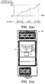
- FIG. 3(a) and FIG. 3(b) are a view illustrating an accumulated operation time displayed by the power-supply device according to the embodiment of the present invention and an example of display thereof.
- FIG. 3(a) represents a relation between a time and an accumulated operation time. The accumulated operation time is added to only in a period in which AC input is present in the power-supply section 10, and the accumulated operation time is not added to in a period in which no AC input is present.
- the computing circuit 22 accumulates the accumulated operation time only for a time for which the DC output power is generated at the power-supply section 10, and thereby can calculate the accumulated operation time.
- the accumulated operation time is obtained by accumulating the time for which the DC output power is generated, and an influence or the like of an amount of deterioration or an ambient temperature of an electrolytic capacitor mounted in a power supply is not considered.
- the computing circuit 22 controls the display circuit 23 such that "accumulated operation time” and "50kh” are displayed on the display circuit 23 ( FIG. 3(b) ).
- the display circuit 23 will be described as an LCD. That is, when a user wants to display the accumulated operation time as the information about the lifespan of the power-supply section 10, the user pushes the switch 24 down, and switches the displayed content of the display circuit 23 to the accumulated operation time, and thereby can obtain the display of FIG. 3(b) .
- the computing circuit 22 calculates the remaining lifespan time based on the amount of deterioration or the ambient temperature of the electrolytic capacitor, and computes information about the lifespan of the power-supply section 10.
- the electrolytic capacitor used in the smoothing circuit 15 or the like of the power-supply device 100 from the time of production, an impregnated electrolyte penetrates a sealing rubber, vaporization of the internal electrolyte advances over time, and deterioration of characteristics including a reduction in capacitance occurs.
- a lifespan of the electrolytic capacitor is greatly dependent on the lifespan of the power-supply section 10. Accordingly, the computing circuit 22 calculates the remaining lifespan time of the power-supply section 10 on the basis of the amount of deterioration of the electrolytic capacitor which is the information from the power-supply section 10.
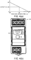
- FIG. 4(a) and FIG. 4(b) are a view illustrating a remaining lifespan time displayed by the power-supply device according to the embodiment of the present invention and an example of display thereof.
- FIG. 4(a) is a graph illustrating a relation between a capacity of the electrolytic capacitor and the remaining lifespan time of the power-supply section 10.
- the longitudinal axis of FIG. 4(a) indicates the capacity of the electrolytic capacitor when a capacity of the electrolytic capacitor at the time of replacement is set to 0%, and a capacity at the time of production is set to 100%. That is, a reduction in the capacity of the electrolytic capacitor indicates the amount of deterioration of the electrolytic capacitor.
- the transverse axis of FIG. 4(a) indicates the remaining lifespan time of the power-supply section 10.
- the remaining lifespan time of the power-supply section 10 is set to 100 kh.
- the remaining lifespan time of the power-supply section 10 is set to 0 kh.
- the computing circuit 22 calculates the remaining lifespan time of the power-supply section 10 at 50 kh as illustrated in FIG. 4(a) . For this reason, the computing circuit 22 controls the display circuit 23 such that "remaining lifespan time" and "50 kh” are displayed on the display circuit 23 ( FIG. 4(b) ). That is, when a user wants to display the remaining lifespan time as the information about the lifespan of the power-supply section 10, the user pushes the switch 24 down, and switches the displayed content of the display circuit 23 to the remaining lifespan time, and thereby can obtain display of FIG. 4(b) .
- the amount of deterioration of the electrolytic capacitor is greatly changed by the ambient temperature.
- the amount of deterioration of the electrolytic capacitor approximately doubles when the ambient temperature is changed by about 10°C according to the chemical reaction kinetics of Arrhenius.
- the graph illustrated in FIG. 4(a) is an ambient temperature of 40°C
- a slope (an absolute value) of the graph increases.
- the ambient temperature is lower than 40°C
- the slope (the absolute value) of the graph decreases.
- the computing circuit 22 may be configured to monitor a temperature inside the power supply during operation using a temperature sensor (not shown), and to calculate the amount of deterioration of the electrolytic capacitor from an operation time and an internal temperature.
- the computing circuit 22 may be configured to monitor an input voltage during operation or the load, and to calculate the amount of deterioration of the electrolytic capacitor from operation times and monitoring amounts thereof.
- the accumulated operation time indicates a time for which the power-supply section 10 has been operated
- the remaining lifespan time indicates a time for which the power-supply section 10 can be operated thereafter.
- it cannot be known to what degree of the lifespan the power-supply section 10 has been operated.
- the user himself/herself cannot switch the display to find out to what degree of the lifespan the power-supply section 10 has been operated.
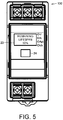
- the computing circuit 22 combines the calculated accumulated operation time and the calculated remaining lifespan time, and thereby can indicate a remaining ratio of the lifespan. To be specific, the computing circuit 22 calculates the remaining ratio of the lifespan as [Remaining lifespan time/(Remaining lifespan time + Accumulated operation time) ⁇ 100](%).
- FIG. 5 is a view illustrating an example of display of a remaining ratio of a lifespan displayed by the power-supply device according to the embodiment of the present invention and an example of display thereof.
- the user when the user wants to display the remaining ratio of the lifespan as the information about the lifespan of the power-supply section 10, the user pushes the switch 24 down and switches the displayed content of the display circuit 23 to the remaining ratio of the lifespan, and thereby can obtain the display of FIG. 5 .
- the remaining ratio of the lifespan is displayed on the display circuit 23, and thereby the user can know a time for which the device has been operated and a time for which it can be operated thereafter, and know to what degree of the lifespan the power-supply section 10 has been operated. Thereby, a difference between the time for which it has been operated and an actual estimate of the remaining lifespan time can be understood and used as a reference for improving the device.
- FIG. 6 is a flow chart for describing a process of displaying information about a lifespan with the power-supply device according to the embodiment of the present invention.
- the computing circuit 22 determines whether the switching signal is input by pushing the switch 24 down or is received by the communication circuit 25 (step S11). When it is determined that the switching signal is input or received (YES in step S11), the computing circuit 22 displays the calculated remaining ratio of the lifespan ( FIG. 5 ) on the display circuit 23 (step S12). When it is determined that the switching signal is not input or received (NO in step S11), the computing circuit 22 enters a waiting state for the input or the reception of the switching signal. That is, when the switching signal is input without the information about the lifespan of the power-supply section 10 displayed on the display circuit 23, the input or the like is triggered to display the information about the lifespan of the power-supply section 10 on the display circuit 23.
- the computing circuit 22 determines whether the switching signal is input by pushing the switch 24 down or is received by the communication circuit 25 within a predetermined time (step S13). When it is determined that the switching signal is input or received within a predetermined time (YES in step S13), the computing circuit 22 displays the calculated accumulated operation time ( FIG. 3(b) ) on the display circuit 23 (step S14). When it is determined that the switching signal is not input or received within a predetermined time (NO in step S13), the computing circuit 22 completes the display of the information about the lifespan of the power-supply section 10.
- step S11 once the information about the lifespan of the power-supply section 10 is temporarily displayed by the input or the like of the switching signal in step S11, if there is an input or the like of the switching signal, the information about the lifespan of the power-supply section 10 is switched.
- the computing circuit 22 determines whether the switching signal is input by pushing the switch 24 down or is received by the communication circuit 25 within a predetermined time (step S15). When it is determined that the switching signal is input or received within a predetermined time (YES in step S15), the computing circuit 22 displays the calculated remaining lifespan time ( FIG. 4(b) ) on the display circuit 23 (step S16). When it is determined that the switching signal is not input or received within a predetermined time (NO in step S15), the computing circuit 22 completes the display of the information about the lifespan of the power-supply section 10.
- the computing circuit 22 determines whether the switching signal is input by pushing the switch 24 down or is received by the communication circuit 25 within a predetermined time (step S17). When it is determined that the switching signal is input or received within a predetermined time (YES in step S17), the process returns to step 12, and the computing circuit 22 displays the calculated remaining ratio of the lifespan ( FIG. 5 ) on the display circuit 23. When it is determined that the switching signal is not input or received within a predetermined time (NO in step S17), the computing circuit 22 completes the display of the information about the lifespan of the power-supply section 10.
- the display can be switched in the order of the remaining ratio of the lifespan, the accumulated operation time, and the remaining lifespan time by the input or the like of the switching signal.
- the power-supply device 100 includes the power-supply section 10, the timing circuit 21, the computing circuit 22, and the display circuit 23.
- the display circuit 23 can display the accumulated operation time and the remaining lifespan time as the information about the lifespan of the power-supply section 10. For this reason, according to the power-supply device 100, the difference between the time for which the device has been operated and an estimate of the actual remaining lifespan time can be understood and used as a reference for improving the device.
- the display circuit 23 has been described as switching display of the remaining ratio of the lifespan, the accumulated operation time, and the remaining lifespan time in that order. However, without being limited thereto, the remaining ratio of the lifespan, the accumulated operation time, and the remaining lifespan time may be displayed on the same display circuit 23.
- the display circuit 23 has been described as switching display in the order of the remaining ratio of the lifespan, the accumulated operation time, and the remaining lifespan time with the input or the like of the switching signal within a predetermined time. However, without being limited thereto, the display circuit 23 may automatically switch the display in the order of the remaining ratio of the lifespan, the accumulated operation time, and the remaining lifespan time even without the input or the like of the switching signal within a predetermined time.
- the switch 24 functions as operating means for displaying the information about the lifespan of the power-supply section 10 on the display circuit 23 or switching the display. However, a function of another operation (e.g., displaying a voltage value) may be assigned.
Landscapes
- Engineering & Computer Science (AREA)
- Power Engineering (AREA)
- Physics & Mathematics (AREA)
- General Physics & Mathematics (AREA)
- Human Computer Interaction (AREA)
- Manufacturing & Machinery (AREA)
- Automation & Control Theory (AREA)
- Dc-Dc Converters (AREA)
- Control Of Indicators Other Than Cathode Ray Tubes (AREA)
Applications Claiming Priority (1)
| Application Number | Priority Date | Filing Date | Title |
|---|---|---|---|
| JP2017047400A JP6844343B2 (ja) | 2017-03-13 | 2017-03-13 | 電源装置 |
Publications (2)
| Publication Number | Publication Date |
|---|---|
| EP3376321A1 true EP3376321A1 (de) | 2018-09-19 |
| EP3376321B1 EP3376321B1 (de) | 2020-04-15 |
Family
ID=60937509
Family Applications (1)
| Application Number | Title | Priority Date | Filing Date |
|---|---|---|---|
| EP17207728.1A Active EP3376321B1 (de) | 2017-03-13 | 2017-12-15 | Stromversorgungsvorrichtung |
Country Status (3)
| Country | Link |
|---|---|
| EP (1) | EP3376321B1 (de) |
| JP (1) | JP6844343B2 (de) |
| CN (1) | CN108696100B (de) |
Families Citing this family (3)
| Publication number | Priority date | Publication date | Assignee | Title |
|---|---|---|---|---|
| JP7014121B2 (ja) * | 2018-10-03 | 2022-02-01 | オムロン株式会社 | 電源システム、電源装置の動作状態表示法、およびプログラム |
| JP7826280B2 (ja) * | 2021-03-01 | 2026-03-09 | 能美防災株式会社 | 煙監視システム |
| CN114019853A (zh) * | 2021-10-27 | 2022-02-08 | 广州祥驰电气有限公司 | 导轨式5g开关电源 |
Citations (3)
| Publication number | Priority date | Publication date | Assignee | Title |
|---|---|---|---|---|
| JP2001091413A (ja) | 1999-09-20 | 2001-04-06 | Hitachi Ltd | 電子機器の寿命監視装置 |
| GB2430039A (en) * | 2005-09-07 | 2007-03-14 | Motorola Inc | Product age monitoring device and method of use of the device |
| US20120136587A1 (en) * | 2010-11-30 | 2012-05-31 | Roopesh Bhaskaran Nagathil | Method and system for machine condition monitoring |
Family Cites Families (9)
| Publication number | Priority date | Publication date | Assignee | Title |
|---|---|---|---|---|
| JPH04186285A (ja) * | 1990-11-21 | 1992-07-03 | Toshiba Corp | 表示端末の寿命情報提供装置 |
| JPH05281001A (ja) * | 1992-04-03 | 1993-10-29 | Fuji Electric Co Ltd | 部品の寿命時間予測装置 |
| JPH09305441A (ja) * | 1996-05-13 | 1997-11-28 | Dainippon Printing Co Ltd | 寿命表示装置 |
| JP2004177156A (ja) * | 2002-11-25 | 2004-06-24 | Topy Ind Ltd | 疲労診断機能付き構造物及びその疲労診断方法 |
| JP5840850B2 (ja) * | 2011-03-25 | 2016-01-06 | 東芝シュネデール・インバータ株式会社 | インバータ装置及び電解コンデンサの寿命時間推定方法 |
| JP5663393B2 (ja) * | 2011-04-28 | 2015-02-04 | 日立建機株式会社 | 稼働機械及び保守点検情報生成装置 |
| CN105938183B (zh) * | 2016-05-06 | 2018-11-02 | 思创数码科技股份有限公司 | 一种预测ups电池寿命的智能监测系统 |
| CN105978150B (zh) * | 2016-06-16 | 2019-07-23 | 顺特电气设备有限公司 | 智能变压器终端的监控方法 |
| WO2018109831A1 (ja) * | 2016-12-13 | 2018-06-21 | 株式会社Fuji | 作業機 |
-
2017
- 2017-03-13 JP JP2017047400A patent/JP6844343B2/ja active Active
- 2017-12-15 EP EP17207728.1A patent/EP3376321B1/de active Active
- 2017-12-18 CN CN201711370143.1A patent/CN108696100B/zh active Active
Patent Citations (3)
| Publication number | Priority date | Publication date | Assignee | Title |
|---|---|---|---|---|
| JP2001091413A (ja) | 1999-09-20 | 2001-04-06 | Hitachi Ltd | 電子機器の寿命監視装置 |
| GB2430039A (en) * | 2005-09-07 | 2007-03-14 | Motorola Inc | Product age monitoring device and method of use of the device |
| US20120136587A1 (en) * | 2010-11-30 | 2012-05-31 | Roopesh Bhaskaran Nagathil | Method and system for machine condition monitoring |
Also Published As
| Publication number | Publication date |
|---|---|
| CN108696100A (zh) | 2018-10-23 |
| JP2018152994A (ja) | 2018-09-27 |
| EP3376321B1 (de) | 2020-04-15 |
| CN108696100B (zh) | 2020-07-31 |
| JP6844343B2 (ja) | 2021-03-17 |
Similar Documents
| Publication | Publication Date | Title |
|---|---|---|
| US8593837B2 (en) | Power supply device and method, based on power supply mode, for image forming apparatus | |
| EP3376321B1 (de) | Stromversorgungsvorrichtung | |
| KR100806774B1 (ko) | Ac/dc 변환기 및 이를 이용한 ac/dc 변환 방법 | |
| WO2007078911A3 (en) | Ripple reduction method for electronic ballasts | |
| JP2004101518A (ja) | 消費電力測定装置、消費電力計算方法、消費電力計算装置、スイッチングモード電源 | |
| CN112534699A (zh) | 电源装置及电源系统 | |
| TWI662393B (zh) | Power supply unit | |
| EP2702674B1 (de) | Leistungsfaktorkorrektur | |
| EP1494342A2 (de) | Schaltungsanordung zur Unterspannungserkennung | |
| EP3609296A1 (de) | Stromversorgungsvorrichtung | |
| US10054647B2 (en) | Fault detection | |
| CN104412707A (zh) | 用于发光装置的操作设备以及操作设备的操作方法 | |
| JP2008306889A (ja) | 無停電電源装置 | |
| JP2000308339A (ja) | スイッチング電源装置 | |
| KR101745102B1 (ko) | 친환경차량용 전력변환기의 출력제어장치 및 방법 | |
| JP5660656B2 (ja) | 電源装置、照明装置、及び、電力計測システム | |
| KR102059204B1 (ko) | Ac-오프 상태를 감지하는 전원공급장치 | |
| US8374013B2 (en) | Power supply with an interface for AC and DC signals | |
| KR101564449B1 (ko) | 전원 공급 장치 | |
| JP6724337B2 (ja) | 点灯装置 | |
| WO2012146695A2 (en) | Electronic driver for a lightsource | |
| JP5803004B2 (ja) | Led点灯装置 | |
| US8441200B2 (en) | Electronic ballast and method for operating at least one first and second discharge lamp | |
| JP2024055427A (ja) | 降圧型定電流回路及び点灯装置 | |
| JP4413659B2 (ja) | 電源装置 |
Legal Events
| Date | Code | Title | Description |
|---|---|---|---|
| PUAI | Public reference made under article 153(3) epc to a published international application that has entered the european phase |
Free format text: ORIGINAL CODE: 0009012 |
|
| STAA | Information on the status of an ep patent application or granted ep patent |
Free format text: STATUS: REQUEST FOR EXAMINATION WAS MADE |
|
| 17P | Request for examination filed |
Effective date: 20171215 |
|
| AK | Designated contracting states |
Kind code of ref document: A1 Designated state(s): AL AT BE BG CH CY CZ DE DK EE ES FI FR GB GR HR HU IE IS IT LI LT LU LV MC MK MT NL NO PL PT RO RS SE SI SK SM TR |
|
| AX | Request for extension of the european patent |
Extension state: BA ME |
|
| RBV | Designated contracting states (corrected) |
Designated state(s): AL AT BE BG CH CY CZ DE DK EE ES FI FR GB GR HR HU IE IS IT LI LT LU LV MC MK MT NL NO PL PT RO RS SE SI SK SM TR |
|
| REG | Reference to a national code |
Ref country code: DE Ref legal event code: R079 Ref document number: 602017014754 Country of ref document: DE Free format text: PREVIOUS MAIN CLASS: G05B0019406500 Ipc: H02M0001000000 |
|
| GRAP | Despatch of communication of intention to grant a patent |
Free format text: ORIGINAL CODE: EPIDOSNIGR1 |
|
| STAA | Information on the status of an ep patent application or granted ep patent |
Free format text: STATUS: GRANT OF PATENT IS INTENDED |
|
| RIC1 | Information provided on ipc code assigned before grant |
Ipc: H02M 1/00 20060101AFI20191015BHEP Ipc: G05B 19/4065 20060101ALI20191015BHEP Ipc: H02M 3/157 20060101ALI20191015BHEP |
|
| INTG | Intention to grant announced |
Effective date: 20191118 |
|
| GRAS | Grant fee paid |
Free format text: ORIGINAL CODE: EPIDOSNIGR3 |
|
| GRAA | (expected) grant |
Free format text: ORIGINAL CODE: 0009210 |
|
| STAA | Information on the status of an ep patent application or granted ep patent |
Free format text: STATUS: THE PATENT HAS BEEN GRANTED |
|
| AK | Designated contracting states |
Kind code of ref document: B1 Designated state(s): AL AT BE BG CH CY CZ DE DK EE ES FI FR GB GR HR HU IE IS IT LI LT LU LV MC MK MT NL NO PL PT RO RS SE SI SK SM TR |
|
| REG | Reference to a national code |
Ref country code: CH Ref legal event code: EP |
|
| REG | Reference to a national code |
Ref country code: DE Ref legal event code: R096 Ref document number: 602017014754 Country of ref document: DE |
|
| REG | Reference to a national code |
Ref country code: IE Ref legal event code: FG4D |
|
| REG | Reference to a national code |
Ref country code: AT Ref legal event code: REF Ref document number: 1258459 Country of ref document: AT Kind code of ref document: T Effective date: 20200515 |
|
| REG | Reference to a national code |
Ref country code: NL Ref legal event code: MP Effective date: 20200415 |
|
| REG | Reference to a national code |
Ref country code: LT Ref legal event code: MG4D |
|
| PG25 | Lapsed in a contracting state [announced via postgrant information from national office to epo] |
Ref country code: LT Free format text: LAPSE BECAUSE OF FAILURE TO SUBMIT A TRANSLATION OF THE DESCRIPTION OR TO PAY THE FEE WITHIN THE PRESCRIBED TIME-LIMIT Effective date: 20200415 Ref country code: PT Free format text: LAPSE BECAUSE OF FAILURE TO SUBMIT A TRANSLATION OF THE DESCRIPTION OR TO PAY THE FEE WITHIN THE PRESCRIBED TIME-LIMIT Effective date: 20200817 Ref country code: NL Free format text: LAPSE BECAUSE OF FAILURE TO SUBMIT A TRANSLATION OF THE DESCRIPTION OR TO PAY THE FEE WITHIN THE PRESCRIBED TIME-LIMIT Effective date: 20200415 Ref country code: FI Free format text: LAPSE BECAUSE OF FAILURE TO SUBMIT A TRANSLATION OF THE DESCRIPTION OR TO PAY THE FEE WITHIN THE PRESCRIBED TIME-LIMIT Effective date: 20200415 Ref country code: IS Free format text: LAPSE BECAUSE OF FAILURE TO SUBMIT A TRANSLATION OF THE DESCRIPTION OR TO PAY THE FEE WITHIN THE PRESCRIBED TIME-LIMIT Effective date: 20200815 Ref country code: SE Free format text: LAPSE BECAUSE OF FAILURE TO SUBMIT A TRANSLATION OF THE DESCRIPTION OR TO PAY THE FEE WITHIN THE PRESCRIBED TIME-LIMIT Effective date: 20200415 Ref country code: NO Free format text: LAPSE BECAUSE OF FAILURE TO SUBMIT A TRANSLATION OF THE DESCRIPTION OR TO PAY THE FEE WITHIN THE PRESCRIBED TIME-LIMIT Effective date: 20200715 Ref country code: GR Free format text: LAPSE BECAUSE OF FAILURE TO SUBMIT A TRANSLATION OF THE DESCRIPTION OR TO PAY THE FEE WITHIN THE PRESCRIBED TIME-LIMIT Effective date: 20200716 |
|
| REG | Reference to a national code |
Ref country code: AT Ref legal event code: MK05 Ref document number: 1258459 Country of ref document: AT Kind code of ref document: T Effective date: 20200415 |
|
| PG25 | Lapsed in a contracting state [announced via postgrant information from national office to epo] |
Ref country code: RS Free format text: LAPSE BECAUSE OF FAILURE TO SUBMIT A TRANSLATION OF THE DESCRIPTION OR TO PAY THE FEE WITHIN THE PRESCRIBED TIME-LIMIT Effective date: 20200415 Ref country code: LV Free format text: LAPSE BECAUSE OF FAILURE TO SUBMIT A TRANSLATION OF THE DESCRIPTION OR TO PAY THE FEE WITHIN THE PRESCRIBED TIME-LIMIT Effective date: 20200415 Ref country code: BG Free format text: LAPSE BECAUSE OF FAILURE TO SUBMIT A TRANSLATION OF THE DESCRIPTION OR TO PAY THE FEE WITHIN THE PRESCRIBED TIME-LIMIT Effective date: 20200715 Ref country code: HR Free format text: LAPSE BECAUSE OF FAILURE TO SUBMIT A TRANSLATION OF THE DESCRIPTION OR TO PAY THE FEE WITHIN THE PRESCRIBED TIME-LIMIT Effective date: 20200415 |
|
| PG25 | Lapsed in a contracting state [announced via postgrant information from national office to epo] |
Ref country code: AL Free format text: LAPSE BECAUSE OF FAILURE TO SUBMIT A TRANSLATION OF THE DESCRIPTION OR TO PAY THE FEE WITHIN THE PRESCRIBED TIME-LIMIT Effective date: 20200415 |
|
| REG | Reference to a national code |
Ref country code: DE Ref legal event code: R097 Ref document number: 602017014754 Country of ref document: DE |
|
| PG25 | Lapsed in a contracting state [announced via postgrant information from national office to epo] |
Ref country code: ES Free format text: LAPSE BECAUSE OF FAILURE TO SUBMIT A TRANSLATION OF THE DESCRIPTION OR TO PAY THE FEE WITHIN THE PRESCRIBED TIME-LIMIT Effective date: 20200415 Ref country code: RO Free format text: LAPSE BECAUSE OF FAILURE TO SUBMIT A TRANSLATION OF THE DESCRIPTION OR TO PAY THE FEE WITHIN THE PRESCRIBED TIME-LIMIT Effective date: 20200415 Ref country code: CZ Free format text: LAPSE BECAUSE OF FAILURE TO SUBMIT A TRANSLATION OF THE DESCRIPTION OR TO PAY THE FEE WITHIN THE PRESCRIBED TIME-LIMIT Effective date: 20200415 Ref country code: EE Free format text: LAPSE BECAUSE OF FAILURE TO SUBMIT A TRANSLATION OF THE DESCRIPTION OR TO PAY THE FEE WITHIN THE PRESCRIBED TIME-LIMIT Effective date: 20200415 Ref country code: SM Free format text: LAPSE BECAUSE OF FAILURE TO SUBMIT A TRANSLATION OF THE DESCRIPTION OR TO PAY THE FEE WITHIN THE PRESCRIBED TIME-LIMIT Effective date: 20200415 Ref country code: IT Free format text: LAPSE BECAUSE OF FAILURE TO SUBMIT A TRANSLATION OF THE DESCRIPTION OR TO PAY THE FEE WITHIN THE PRESCRIBED TIME-LIMIT Effective date: 20200415 Ref country code: AT Free format text: LAPSE BECAUSE OF FAILURE TO SUBMIT A TRANSLATION OF THE DESCRIPTION OR TO PAY THE FEE WITHIN THE PRESCRIBED TIME-LIMIT Effective date: 20200415 Ref country code: DK Free format text: LAPSE BECAUSE OF FAILURE TO SUBMIT A TRANSLATION OF THE DESCRIPTION OR TO PAY THE FEE WITHIN THE PRESCRIBED TIME-LIMIT Effective date: 20200415 |
|
| PLBE | No opposition filed within time limit |
Free format text: ORIGINAL CODE: 0009261 |
|
| STAA | Information on the status of an ep patent application or granted ep patent |
Free format text: STATUS: NO OPPOSITION FILED WITHIN TIME LIMIT |
|
| PG25 | Lapsed in a contracting state [announced via postgrant information from national office to epo] |
Ref country code: SK Free format text: LAPSE BECAUSE OF FAILURE TO SUBMIT A TRANSLATION OF THE DESCRIPTION OR TO PAY THE FEE WITHIN THE PRESCRIBED TIME-LIMIT Effective date: 20200415 Ref country code: PL Free format text: LAPSE BECAUSE OF FAILURE TO SUBMIT A TRANSLATION OF THE DESCRIPTION OR TO PAY THE FEE WITHIN THE PRESCRIBED TIME-LIMIT Effective date: 20200415 |
|
| 26N | No opposition filed |
Effective date: 20210118 |
|
| PG25 | Lapsed in a contracting state [announced via postgrant information from national office to epo] |
Ref country code: SI Free format text: LAPSE BECAUSE OF FAILURE TO SUBMIT A TRANSLATION OF THE DESCRIPTION OR TO PAY THE FEE WITHIN THE PRESCRIBED TIME-LIMIT Effective date: 20200415 |
|
| REG | Reference to a national code |
Ref country code: CH Ref legal event code: PL |
|
| PG25 | Lapsed in a contracting state [announced via postgrant information from national office to epo] |
Ref country code: MC Free format text: LAPSE BECAUSE OF FAILURE TO SUBMIT A TRANSLATION OF THE DESCRIPTION OR TO PAY THE FEE WITHIN THE PRESCRIBED TIME-LIMIT Effective date: 20200415 |
|
| REG | Reference to a national code |
Ref country code: BE Ref legal event code: MM Effective date: 20201231 |
|
| PG25 | Lapsed in a contracting state [announced via postgrant information from national office to epo] |
Ref country code: LU Free format text: LAPSE BECAUSE OF NON-PAYMENT OF DUE FEES Effective date: 20201215 Ref country code: IE Free format text: LAPSE BECAUSE OF NON-PAYMENT OF DUE FEES Effective date: 20201215 Ref country code: FR Free format text: LAPSE BECAUSE OF NON-PAYMENT OF DUE FEES Effective date: 20201231 |
|
| PG25 | Lapsed in a contracting state [announced via postgrant information from national office to epo] |
Ref country code: CH Free format text: LAPSE BECAUSE OF NON-PAYMENT OF DUE FEES Effective date: 20201231 Ref country code: LI Free format text: LAPSE BECAUSE OF NON-PAYMENT OF DUE FEES Effective date: 20201231 |
|
| PG25 | Lapsed in a contracting state [announced via postgrant information from national office to epo] |
Ref country code: TR Free format text: LAPSE BECAUSE OF FAILURE TO SUBMIT A TRANSLATION OF THE DESCRIPTION OR TO PAY THE FEE WITHIN THE PRESCRIBED TIME-LIMIT Effective date: 20200415 Ref country code: MT Free format text: LAPSE BECAUSE OF FAILURE TO SUBMIT A TRANSLATION OF THE DESCRIPTION OR TO PAY THE FEE WITHIN THE PRESCRIBED TIME-LIMIT Effective date: 20200415 Ref country code: CY Free format text: LAPSE BECAUSE OF FAILURE TO SUBMIT A TRANSLATION OF THE DESCRIPTION OR TO PAY THE FEE WITHIN THE PRESCRIBED TIME-LIMIT Effective date: 20200415 |
|
| PG25 | Lapsed in a contracting state [announced via postgrant information from national office to epo] |
Ref country code: MK Free format text: LAPSE BECAUSE OF FAILURE TO SUBMIT A TRANSLATION OF THE DESCRIPTION OR TO PAY THE FEE WITHIN THE PRESCRIBED TIME-LIMIT Effective date: 20200415 |
|
| PG25 | Lapsed in a contracting state [announced via postgrant information from national office to epo] |
Ref country code: BE Free format text: LAPSE BECAUSE OF NON-PAYMENT OF DUE FEES Effective date: 20201231 |
|
| GBPC | Gb: european patent ceased through non-payment of renewal fee |
Effective date: 20211215 |
|
| PG25 | Lapsed in a contracting state [announced via postgrant information from national office to epo] |
Ref country code: GB Free format text: LAPSE BECAUSE OF NON-PAYMENT OF DUE FEES Effective date: 20211215 |
|
| PGFP | Annual fee paid to national office [announced via postgrant information from national office to epo] |
Ref country code: DE Payment date: 20251222 Year of fee payment: 9 |