EP3373330B1 - Aufbau eines elektronischen chips - Google Patents
Aufbau eines elektronischen chips Download PDFInfo
- Publication number
- EP3373330B1 EP3373330B1 EP17187590.9A EP17187590A EP3373330B1 EP 3373330 B1 EP3373330 B1 EP 3373330B1 EP 17187590 A EP17187590 A EP 17187590A EP 3373330 B1 EP3373330 B1 EP 3373330B1
- Authority
- EP
- European Patent Office
- Prior art keywords
- flip
- well
- flops
- logic level
- chip
- Prior art date
- Legal status (The legal status is an assumption and is not a legal conclusion. Google has not performed a legal analysis and makes no representation as to the accuracy of the status listed.)
- Active
Links
Images

Classifications
-
- G—PHYSICS
- G06—COMPUTING OR CALCULATING; COUNTING
- G06K—GRAPHICAL DATA READING; PRESENTATION OF DATA; RECORD CARRIERS; HANDLING RECORD CARRIERS
- G06K19/00—Record carriers for use with machines and with at least a part designed to carry digital markings
- G06K19/06—Record carriers for use with machines and with at least a part designed to carry digital markings characterised by the kind of the digital marking, e.g. shape, nature, code
- G06K19/067—Record carriers with conductive marks, printed circuits or semiconductor circuit elements, e.g. credit or identity cards also with resonating or responding marks without active components
- G06K19/07—Record carriers with conductive marks, printed circuits or semiconductor circuit elements, e.g. credit or identity cards also with resonating or responding marks without active components with integrated circuit chips
- G06K19/073—Special arrangements for circuits, e.g. for protecting identification code in memory
- G06K19/07309—Means for preventing undesired reading or writing from or onto record carriers
- G06K19/07372—Means for preventing undesired reading or writing from or onto record carriers by detecting tampering with the circuit
- G06K19/07381—Means for preventing undesired reading or writing from or onto record carriers by detecting tampering with the circuit with deactivation or otherwise incapacitation of at least a part of the circuit upon detected tampering
-
- G—PHYSICS
- G06—COMPUTING OR CALCULATING; COUNTING
- G06F—ELECTRIC DIGITAL DATA PROCESSING
- G06F21/00—Security arrangements for protecting computers, components thereof, programs or data against unauthorised activity
- G06F21/70—Protecting specific internal or peripheral components, in which the protection of a component leads to protection of the entire computer
- G06F21/71—Protecting specific internal or peripheral components, in which the protection of a component leads to protection of the entire computer to assure secure computing or processing of information
- G06F21/75—Protecting specific internal or peripheral components, in which the protection of a component leads to protection of the entire computer to assure secure computing or processing of information by inhibiting the analysis of circuitry or operation
- G06F21/755—Protecting specific internal or peripheral components, in which the protection of a component leads to protection of the entire computer to assure secure computing or processing of information by inhibiting the analysis of circuitry or operation with measures against power attack
-
- H—ELECTRICITY
- H10—SEMICONDUCTOR DEVICES; ELECTRIC SOLID-STATE DEVICES NOT OTHERWISE PROVIDED FOR
- H10D—INORGANIC ELECTRIC SEMICONDUCTOR DEVICES
- H10D84/00—Integrated devices formed in or on semiconductor substrates that comprise only semiconducting layers, e.g. on Si wafers or on GaAs-on-Si wafers
- H10D84/90—Masterslice integrated circuits
- H10D84/903—Masterslice integrated circuits comprising field effect technology
- H10D84/907—CMOS gate arrays
-
- H—ELECTRICITY
- H10—SEMICONDUCTOR DEVICES; ELECTRIC SOLID-STATE DEVICES NOT OTHERWISE PROVIDED FOR
- H10D—INORGANIC ELECTRIC SEMICONDUCTOR DEVICES
- H10D89/00—Aspects of integrated devices not covered by groups H10D84/00 - H10D88/00
-
- H—ELECTRICITY
- H10—SEMICONDUCTOR DEVICES; ELECTRIC SOLID-STATE DEVICES NOT OTHERWISE PROVIDED FOR
- H10W—GENERIC PACKAGES, INTERCONNECTIONS, CONNECTORS OR OTHER CONSTRUCTIONAL DETAILS OF DEVICES COVERED BY CLASS H10
- H10W42/00—Arrangements for protection of devices
- H10W42/40—Arrangements for protection of devices protecting against tampering, e.g. unauthorised inspection or reverse engineering
- H10W42/405—Arrangements for protection of devices protecting against tampering, e.g. unauthorised inspection or reverse engineering using active circuits
-
- H—ELECTRICITY
- H10—SEMICONDUCTOR DEVICES; ELECTRIC SOLID-STATE DEVICES NOT OTHERWISE PROVIDED FOR
- H10W—GENERIC PACKAGES, INTERCONNECTIONS, CONNECTORS OR OTHER CONSTRUCTIONAL DETAILS OF DEVICES COVERED BY CLASS H10
- H10W74/00—Encapsulations, e.g. protective coatings
- H10W74/01—Manufacture or treatment
- H10W74/012—Manufacture or treatment of encapsulations on active surfaces of flip-chip devices, e.g. forming underfills
-
- H—ELECTRICITY
- H10—SEMICONDUCTOR DEVICES; ELECTRIC SOLID-STATE DEVICES NOT OTHERWISE PROVIDED FOR
- H10W—GENERIC PACKAGES, INTERCONNECTIONS, CONNECTORS OR OTHER CONSTRUCTIONAL DETAILS OF DEVICES COVERED BY CLASS H10
- H10W74/00—Encapsulations, e.g. protective coatings
- H10W74/10—Encapsulations, e.g. protective coatings characterised by their shape or disposition
- H10W74/15—Encapsulations, e.g. protective coatings characterised by their shape or disposition on active surfaces of flip-chip devices, e.g. underfills
-
- H—ELECTRICITY
- H03—ELECTRONIC CIRCUITRY
- H03K—PULSE TECHNIQUE
- H03K19/00—Logic circuits, i.e. having at least two inputs acting on one output; Inverting circuits
- H03K19/003—Modifications for increasing the reliability for protection
- H03K19/00315—Modifications for increasing the reliability for protection in field-effect transistor circuits
-
- H—ELECTRICITY
- H03—ELECTRONIC CIRCUITRY
- H03K—PULSE TECHNIQUE
- H03K3/00—Circuits for generating electric pulses; Monostable, bistable or multistable circuits
- H03K3/02—Generators characterised by the type of circuit or by the means used for producing pulses
- H03K3/353—Generators characterised by the type of circuit or by the means used for producing pulses by the use, as active elements, of field-effect transistors with internal or external positive feedback
- H03K3/356—Bistable circuits
-
- Y—GENERAL TAGGING OF NEW TECHNOLOGICAL DEVELOPMENTS; GENERAL TAGGING OF CROSS-SECTIONAL TECHNOLOGIES SPANNING OVER SEVERAL SECTIONS OF THE IPC; TECHNICAL SUBJECTS COVERED BY FORMER USPC CROSS-REFERENCE ART COLLECTIONS [XRACs] AND DIGESTS
- Y04—INFORMATION OR COMMUNICATION TECHNOLOGIES HAVING AN IMPACT ON OTHER TECHNOLOGY AREAS
- Y04S—SYSTEMS INTEGRATING TECHNOLOGIES RELATED TO POWER NETWORK OPERATION, COMMUNICATION OR INFORMATION TECHNOLOGIES FOR IMPROVING THE ELECTRICAL POWER GENERATION, TRANSMISSION, DISTRIBUTION, MANAGEMENT OR USAGE, i.e. SMART GRIDS
- Y04S40/00—Systems for electrical power generation, transmission, distribution or end-user application management characterised by the use of communication or information technologies, or communication or information technology specific aspects supporting them
- Y04S40/20—Information technology specific aspects, e.g. CAD, simulation, modelling, system security
Definitions
- the present application concerns a particular electronic chip architecture.
- fault injection attack It is desirable to have electronic chips protected against this type of attack, called fault injection attack, the known devices having various drawbacks and implementation difficulties. Reference is made to document F2 2 958 078 A1.
- One embodiment provides a device making it possible to overcome all or part of the drawbacks described above.
- one embodiment provides an electronic chip comprising: a semiconductor substrate doped with a first type of conductivity; boxes of a second type of conductivity on the side of the front face of the chip, in and on which circuit elements are formed; one or more slabs of the second type of conductivity buried under the boxes and separated from the boxes by part of the substrate; for each buried slab, a well of the second type of conductivity, polarizable, which extends from the front face of the substrate to the buried slab; P for each well, at least one flip-flop of the chip comprising, in the upper part of each well, a first channel MOS transistor of the first conductivity type, the first transistor being an element of said at least one flip-flop; and a circuit for detecting a change in logic level of one of the flip-flops.
- the detection circuit is adapted to initialize the flip-flops at a first logic level, and to detect the passage of one of the flip-flops to a second logic level.
- the chip comprises, in the upper part of each well, a second MOS channel transistor of the first conductivity type, the second transistor being an element of an additional flip-flop, the detection circuit being further adapted to initialize the additional flip-flops at the second logic level, and detect the passage of one of the additional flip-flops to the first logic level.
- the chip comprises, in the upper part of each well, a plurality of channel MOS transistors of the first conductivity type, each transistor being an element of a flip-flop, the detection circuit being adapted to detect a change of the logic level of a majority of flip-flops.
- each of said flip-flops comprises several channel MOS transistors of the first conductivity type located in the upper part of the well.
- the buried slabs have a thickness of between 1 and 2 ⁇ m and are separated from the boxes by 1 to 2 ⁇ m.
- the buried slabs are rectangular with sides of more than 40 ⁇ m.
- the buried slabs are rectangular with sides of less than 80 ⁇ m.
- each well has lateral dimensions of between 1 and 3 ⁇ m.
- each well comprises a polarization contact with lateral dimensions of between 100 and 300 nm.
- the detection circuit is adapted to trigger, in the event of detection, countermeasures intended to stop an attack.
- Another embodiment provides a method of protection against an attack on a chip above, comprising successively: a) biasing the wells and initializing the logic levels of the flip-flops; b) detect a change in logic level of one of the flip-flops; and c) trigger countermeasures intended to stop the attack if a change in logic level is detected in step b).
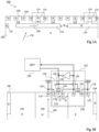
- FIG. 1A is a partial and schematic sectional view of an embodiment of a chip 100 protected against attacks.
- the chip 100 comprises a doped semiconductor substrate 102, for example made of P-type doped silicon.
- the substrate comprises N-type doped boxes 104 which extend from the front face of the chip (upper face).
- the boxes have for example the shape of elongated strips perpendicular to the plane of the figure, as will be described in relation to the figure 3 .
- the boxes 104 of type N are separated from each other by regions 106 of the substrate, of type P.
- Sensitive circuits containing confidential information wished by a hacker, are likely to be formed in and on the boxes 104 and/or or the regions 106.
- the sensitive circuits not shown, include P-channel MOS transistors in and on the wells 104, and N-channel MOS transistors in and on the regions 106.
- N-type doped semiconductor tiles 110 are buried in the substrate 102 under the sensitive circuits.
- the buried slabs are separated from the N boxes 104 by a part 112 of the substrate, doped with type P.
- An N-type doped semiconductor well 114 which extends from the front face of the substrate 102 comes into contact with each of the buried slabs 110, preferably in the center of the buried slab.
- the wells 114 are distinct from the boxes 104, and are separated from the boxes 104 by regions 116 of the P-type substrate.
- FIG. 1B is a schematic enlarged sectional view of the upper part of a well 114.
- Each well 114 is provided with a contact zone 118, connected to a node 120 for applying a high polarization potential VDD.
- a P-type region 116 surrounds the well 114 and is provided with a contact zone 122 connected to a node 124 for applying a reference potential, for example a ground GND.
- a P-channel MOS type transistor TP is located in the upper part of each N well 114.
- the transistor TP comprises source 130 and drain 132 zones, on either side of a channel region 134 located under a isolated gate 136.
- Channel region 134 is an upper part of well N 114.
- Source zone 130 is connected to node 120.
- the transistor TP is connected to an N-channel MOS type transistor TN, preferably located in the region 116 surrounding the well 114, so as to form with it an inverter 138.
- the gates of the interconnected transistors TP and TN correspond to the input node 140 of the inverter 138, and the drains of the interconnected TP and TN transistors correspond to the output node 142 of the inverter 138.
- an inverter 150 represented symbolically, has its input connected to the node 142 and its output connected to node 140.
- the inverter 150 consists of a P-channel MOS transistor, preferably located in well 114, and an N-channel MOS transistor, preferably located in region 116.
- the assembly of the inverter 138 and the inverter 150 connected head to tail constitutes a flip-flop 152, that is to say a logic circuit intended, when an initial logic level is applied to it, to start at this logic level, and, when no logic level is applied to it, to remain at the initial logic level.
- Nodes 140 and 142 are connected to a detection circuit 160 (DET).
- the detection circuit 160 is common to the various flip-flops 152 of the various wells 114.
- the detection circuit is designed to temporarily apply a high logic level to node 140 during a startup phase of the chip, for example when powering up.
- Flip-flop 152 is thus initialized and provides the high level on node 140 and the low level on node 142.
- circuit 160 does not apply any logic level to node 140.
- the detection circuit is designed to detect a change in logic level of the flip-flop, for example on node 142. In the event of a change in this level, the chip takes countermeasures intended to stop an attack, for example by stopping operating, or by destroying confidential data.
- a hacker seeks to disrupt sensitive circuits located above one of the buried slabs 110, from the rear side, for example by laser 170. Due to the fact that the slab 110 is polarized at the potential VDD, it collects photogenerated electrons, and these electrons move towards the contact zone 118 (arrows 180 illustrated in Figures 1A and 1B ). The presence of electrons near zone 118 reduces the potential of region 114 located under transistor TP, which becomes conducting (current I1). The potential of node 142 goes high, and the flip-flop changes logic level. This change in logic level triggers the implementation of countermeasures, and the attack is countered.
- the sensitive circuits located above one of the buried slabs 110 are thus protected against laser attacks.
- a distance D smaller than the diameter of the laser can be provided between neighboring tiles 110, for example the smallest possible distance, for example less than 4 ⁇ m. We thus obtain protection of all of the sensitive circuits of the chip against laser attacks.
- the attack is detected and countered in the same way as a laser attack. Indeed, the PN junction between the slab 110 and the substrate 102 enters into an avalanche and electrons are collected by the slab 110 towards the upper part of the well.
- the PN junction between the panel 110 and the substrate 102 is conducting, and the attack is also detected and countered.
- the chip is protected against various types of fault injection attacks in a particularly simple to implement manner.
- the use of flip-flop 152 makes it possible to counter attacks without using analog components such as various current sources or various resistors, which are difficult to implement and adjust.
- the contact zone 118 is small, with lateral dimensions for example less than 300 nm, for example between 100 and 300 nm. Therefore, the The resistance that zone 118 opposes to the evacuation of electrons towards potential VDD is high, which makes it possible to detect the attack in a particularly sensitive manner. We obtain particularly effective protection against attacks.
- the boxes 104 extend to a depth of between 1 and 2 ⁇ m.
- the thickness of the P-type part 112, between the N boxes 104 and the slabs 110, is between 1 and 2 ⁇ m.
- the thickness of buried slabs is between 1 and 2 ⁇ m.
- the detection circuit can be provided to temporarily apply to node 140, during the start-up phase, the low logic level, thus initializing the flip-flop in the opposite manner to that described previously.
- the circuit 160 detects a transition to a low logic level of the node 142. Indeed, in the event of an attack by laser, or in the event of an attack by a high negative potential probe, the presence of electrons in the well 114 turns on the bipolar transistor consisting of the drain region 132 of the transistor TP, the well N 114, and the region P 116 (current I2), which causes a drop in the potential of the node 142.
- attacks are detected which cause node 142 to go to the low logic level, instead of to the high logic level described above.
- the direction of the logic level change depends in fact on various parameters of the attack such as its duration and/or its intensity, and on the configuration of the transistor TP, of the zone 118 and of the upper part of the well 114, in particular their shapes and arrangement. We can choose this configuration to favor one direction of change of logical level compared to the other direction.
- a single contact zone 118 is represented in Figure 1B , several contact zones 118 can be used for the same well 114, in order to influence the sensitivity and direction of the logic level change.
- FIG 2 illustrates an embodiment of a chip 200 protected against attacks, comprising the same elements as the chip 100 of the Figures 1A and 1B , arranged in a similar way.
- the chip 200 includes a second flip-flop 152' similar to the flip-flop 152.
- the second flip-flop 152' includes in particular a transistor TP 'P-channel MOS type located in and on the upper part of well 114.
- the detection circuit is designed to initialize, during the start-up phase of the chip, flip-flop 152 at the low logic level on the drain node 142 of transistor TP, and flip-flop 152' at the high logic level on node 142 'drain of transistor TP'. Flip-flops 152 and 152' are thus initialized at different logic levels.
- the detection circuit is designed to detect the change in logic level of flip-flop 152 and/or flip-flop 152'.
- the level of detection sensitivity of the attack corresponds to the direction of change which occurs with the greatest sensitivity. Attacks are thus detected with particularly high sensitivity, and the level of protection is particularly high. In addition, we obtain a level of high protection without choosing to favor one or the other direction of logic level change by a particular configuration of the elements in the upper part of the well, which makes it possible to obtain this level of protection in a particularly simple manner.
- FIG. 3 is a partial and schematic top view of a chip of the type of chip 100 of the Figures 1A and 1B or chip 200 of the figure 2 .
- the N boxes 104 and the P regions 106 form alternating parallel strips above the buried slabs 110.
- the sensitive circuits are for example logic circuits comprising, as mentioned above, P-channel MOS transistors and N-channel MOS transistors located in and on neighboring bands 104 and 106.
- the widths of the bands are between 1 and 3 ⁇ m.
- the buried slabs are rectangular, preferably square.
- the dimensions of the sides of the buried slabs are for example between 40 and 80 ⁇ m.
- the buried slabs are preferably arranged regularly.
- the wells 114 are preferably located at the centers of the slabs.
- the wells 114, surrounded by the regions 116, are located at the location of bands 104 which are interrupted to make room for them.
- the wells 114 preferably have, in top view, a square shape of the same dimensions as the width of the strips 104, aligned with the strips 104.
- the surface of the chip occupied by the protection elements is particularly small. Indeed, the protection elements associated with only one of the wells 114 make it possible to protect all the sensitive circuits located above the buried slab 110 considered, the latter having for example more than 40 ⁇ m side.
- the dimensions of the sides of the slabs are for example less than 80 ⁇ m, and the fact that the wells 114 are in a central position on the buried slabs, a possible attack is detected quickly.
- the electrons collected by the slab 110 concerned then have a short distance to travel to reach the upper part of the well 114.
- the protection device is particularly simple to produce at the same time as the logic circuits of the chip.
- the flip-flops are logic circuits comprising N-channel and P-channel MOS transistors which can be produced in and on the wells 114 and the regions 116 at the same time and in the same manner as the MOS transistors of the logic circuits of the chip.
- any type of flip-flop can be used comprising a P-channel MOS transistor whose channel region is a part of the well 114, this flip-flop being such that the change in on/off state of the transistor causes the change in the logic level of the flip-flop.
- the flip-flop may include several P-channel MOS transistors whose channel regions are portions of well 114.
- the chip 100 includes a flip-flop for each well 114 and the chip 200 includes two flip-flops for each well 114, more than two flip-flops can be provided for each well 114, each flip-flop comprising each, like the flip-flops of the chips 100 and 200, at least one transistor in and on the well 114.
- the detection circuit can then be adapted to detect for one of the wells 114 a change in logic level of a majority of the flip-flops. This eliminates the risk that only one of the flip-flops causes, through excessive sensitivity, the countermeasures to be triggered in the absence of an attack.
- the embodiments described include several buried slabs 110, each connected to a well 114, it will be noted that it is possible to provide a single slab buried under all of the sensitive circuits, connected to a single well 114.
- the tiles can have dimensions greater than 80 ⁇ m, for example more than 1 mm.
- the slab can be rectangular with sides of more than 1 mm.
Landscapes
- Engineering & Computer Science (AREA)
- Computer Hardware Design (AREA)
- Physics & Mathematics (AREA)
- Theoretical Computer Science (AREA)
- General Physics & Mathematics (AREA)
- General Engineering & Computer Science (AREA)
- Computer Security & Cryptography (AREA)
- Microelectronics & Electronic Packaging (AREA)
- Software Systems (AREA)
- Mathematical Physics (AREA)
- Semiconductor Integrated Circuits (AREA)
- Storage Device Security (AREA)
- Automation & Control Theory (AREA)
Claims (12)
- Elektronischer Chip, der Folgendes aufweist:ein dotiertes Halbleitersubstrat (102) eines ersten Leitfähigkeitstyps; Kästen (104) eines zweiten Leitfähigkeitstyps auf der Vorderseite des Chips, in und auf denen Schaltungselemente ausgebildet sind;eine oder mehrere Platten (110) des zweiten Leitfähigkeitstyps, die unter den Kästen vergraben und von den Kästen durch einen Teil des Substrats getrennt sind;für jede vergrabene Platte eine polarisierbare Wanne (114) des zweiten Leitfähigkeitstyps, die sich von der Vorderseite des Substrats bis zur vergrabenen Platte erstreckt;für jede Wanne mindestens ein Flip-Flop des Chips, das in einem oberen Abschnitt der Wanne einen ersten MOS-Transistor (TP) mit einem Kanal des ersten Leitfähigkeitstyps aufweist, wobei der erste Transistor ein Element des mindestens einen Flip-Flops (152) ist; undeine Schaltung zum Detektieren (160) einer Änderung des Logigpegels eines der Flip-Flops.
- Chip nach Anspruch 1, wobei die Detektierschaltung (160) so ausgelegt ist, dass sie die Flip-Flops (152) auf einem ersten Logikpegel initialisiert und den Übergang eines der Flip-Flops auf einen zweiten Logikpegel detektiert.
- Chip nach Anspruch 2, der im oberen Teil jeder Wanne einen zweiten MOS-Transistor (TP') mit einem Kanal des ersten Leitfähigkeitstyps aufweist, wobei der zweite Transistor ein Element eines zusätzlichen Flip-Flops (152') ist, wobei die Detektierschaltung (160) außerdem so beschaffen ist, dass sie die zusätzlichen Flip-Flops auf dem zweiten Logikpegel initialisiert und den Übergang eines der zusätzlichen Flip-Flops auf den ersten Logikpegel detektiert.
- Chip nach einem der Ansprüche 1 bis 3, der im oberen Teil jeder Wanne eine Vielzahl von MOS-Transistoren (TP, TP') mit Kanälen des ersten Leitfähigkeitstyps aufweist, wobei jeder Transistor ein Element eines Flip-Flops (152, 152') ist, wobei die Detektierschaltung so beschaffen ist, dass sie eine Änderung des Logikpegels einer Mehrheit der Flip-Flops detektiert.
- Chip nach einem der Ansprüche 1 bis 4, wobei für jede Wanne (114) jedes der Flip-Flops (152) mehrere MOS-Transistoren mit Kanälen des ersten Leitfähigkeitstyps aufweist, die im oberen Teil der Wanne angeordnet sind.
- Chip nach einem der Ansprüche 1 bis 5, wobei die vergrabenen Platten (114) eine Dicke zwischen 1 und 2 µm aufweisen und von den Kästen um 1 bis 2 µm beabstandet sind.
- Chip nach einem der Ansprüche 1 bis 6, wobei die vergrabenen Platten (114) Rechtecke mit einer Seitenlänge von mehr als 40 µm sind.
- Chip nach einem der Ansprüche 1 bis 7, bei dem die vergrabenen Platten (114) Rechtecke mit einer Seitenlänge von weniger als 80 µm sind.
- Chip nach einem der Ansprüche 1 bis 8, wobei jede Wanne (114) seitliche Abmessungen zwischen 1 und 3 µm aufweist.
- Chip nach einem der Ansprüche 1 bis 9, wobei jede Wanne (114) einen Vorspannkontakt (118) mit seitlichen Abmessungen zwischen 100 und 300 nm aufweist.
- Chip nach einem der Ansprüche 1 bis 10, wobei die Detektierschaltung (160) geeignet ist, im Falle einer Detektierung Gegenmaßnahmen auszulösen.
- Verfahren zum Schutz eines Chips nach einem der Ansprüche 1 bis 11 vor einem Angriff, wobei das Verfahren nacheinander Folgendes aufweist:a) Vorspannen der Wannen und Initialisieren der Logikpegel der Flip-Flops;b) Detektieren einer Änderung des Logikpegels eines der Flip-Flops; undc) Auslösen von Gegenmaßnahmen, die dazu bestimmt sind, den Angriff zu stoppen, wenn in Schritt b) eine Änderung des Logikpegels detektiert wird.
Applications Claiming Priority (1)
| Application Number | Priority Date | Filing Date | Title |
|---|---|---|---|
| FR1751788A FR3063597A1 (fr) | 2017-03-06 | 2017-03-06 | Architecture de puce electronique |
Publications (2)
| Publication Number | Publication Date |
|---|---|
| EP3373330A1 EP3373330A1 (de) | 2018-09-12 |
| EP3373330B1 true EP3373330B1 (de) | 2024-06-19 |
Family
ID=59381361
Family Applications (1)
| Application Number | Title | Priority Date | Filing Date |
|---|---|---|---|
| EP17187590.9A Active EP3373330B1 (de) | 2017-03-06 | 2017-08-23 | Aufbau eines elektronischen chips |
Country Status (3)
| Country | Link |
|---|---|
| US (1) | US10734329B2 (de) |
| EP (1) | EP3373330B1 (de) |
| FR (1) | FR3063597A1 (de) |
Family Cites Families (12)
| Publication number | Priority date | Publication date | Assignee | Title |
|---|---|---|---|---|
| US5736777A (en) * | 1995-12-29 | 1998-04-07 | Intel Corporation | Method and apparatus for fast self-destruction of a CMOS integrated circuit |
| DE10254325A1 (de) * | 2002-11-21 | 2004-06-03 | Philips Intellectual Property & Standards Gmbh | Elektronisches Speicherbauteil |
| JP4497874B2 (ja) * | 2002-12-13 | 2010-07-07 | 株式会社ルネサステクノロジ | 半導体集積回路及びicカード |
| DE102004009622A1 (de) * | 2004-02-27 | 2005-06-16 | Infineon Technologies Ag | Halbleiterbauelement mit einer CMOS-Schaltung |
| US7847581B2 (en) * | 2008-04-03 | 2010-12-07 | Stmicroelectronics (Rousset) Sas | Device for protecting an integrated circuit against a laser attack |
| US8510700B2 (en) * | 2009-02-24 | 2013-08-13 | Syphermedia International, Inc. | Method and apparatus for camouflaging a standard cell based integrated circuit with micro circuits and post processing |
| JP5519308B2 (ja) * | 2010-02-05 | 2014-06-11 | ルネサスエレクトロニクス株式会社 | 半導体集積回路及びデータ処理システム |
| FR2958078B1 (fr) * | 2010-03-24 | 2012-04-20 | St Microelectronics Rousset | Procede et dispositif de contremesure contre une attaque par injection d'erreur dans un microcircuit electronique |
| EP2369622B1 (de) * | 2010-03-24 | 2015-10-14 | STMicroelectronics Rousset SAS | Verfahren und Vorrichtung für Gegenmassnahme gegenüber einem Angriff durch Fehlerinjektion in einem elektronischen Mikroschaltungskarte |
| FR2981783B1 (fr) * | 2011-10-19 | 2014-05-09 | St Microelectronics Rousset | Systeme de detection d'une attaque par laser d'une puce de circuit integre |
| DE102013112552B4 (de) * | 2013-11-14 | 2017-05-24 | Infineon Technologies Ag | Schaltungsanordnung und Verfahren zum Sichern einer Schaltungsanordnung gegen wiederholte Lichtangriffe |
| US9559066B2 (en) * | 2014-06-12 | 2017-01-31 | Broadcom Corporation | Systems and methods for detecting and preventing optical attacks |
-
2017
- 2017-03-06 FR FR1751788A patent/FR3063597A1/fr not_active Withdrawn
- 2017-08-23 EP EP17187590.9A patent/EP3373330B1/de active Active
- 2017-11-02 US US15/801,517 patent/US10734329B2/en active Active
Also Published As
| Publication number | Publication date |
|---|---|
| EP3373330A1 (de) | 2018-09-12 |
| FR3063597A1 (fr) | 2018-09-07 |
| US20180253633A1 (en) | 2018-09-06 |
| US10734329B2 (en) | 2020-08-04 |
Similar Documents
| Publication | Publication Date | Title |
|---|---|---|
| EP2535932B1 (de) | Chip mit einem integrierten Schaltkreis und einer Schutzvorrichtung gegen Angriffe | |
| FR2981783A1 (fr) | Systeme de detection d'une attaque par laser d'une puce de circuit integre | |
| EP2369622B1 (de) | Verfahren und Vorrichtung für Gegenmassnahme gegenüber einem Angriff durch Fehlerinjektion in einem elektronischen Mikroschaltungskarte | |
| EP2535933B1 (de) | Chip mit einem integrierten Schaltkreis und einer Schutzvorrichtung gegen Angriffe | |
| EP2866259B1 (de) | Elektronischer Chip mit Mitteln zum Schutz dessen Rückseite | |
| EP0551038B1 (de) | Allgemeine Schutzvorrichtung eines integrierten Schaltkreises gegen Überlastungen und elektrostatische Entladungen | |
| FR2986356A1 (fr) | Dispositif de protection d'un circuit integre contre des attaques en face arriere | |
| FR2998419A1 (fr) | Protection d'un circuit integre contre des attaques | |
| FR2986633A1 (fr) | Dispositif de detection d'une attaque par laser dans une puce de circuit integre | |
| FR2812972A1 (fr) | Dispositif a semiconducteur consistant en un thyristor pour la protection contre les decharges electrostatiques | |
| EP3301605B1 (de) | Geschützter elektronischer chip | |
| EP3159872B1 (de) | Gesicherter elektronischer chip unter verwendung von multiple-well technologie | |
| EP3151277B1 (de) | Gesicherter integrierter schaltkreis | |
| FR2993404A1 (fr) | Circuit integre sur soi comprenant un thyristor (scr) de protection contre des decharges electrostatiques | |
| FR3005203A1 (fr) | Circuit integre sur soi comprenant un transistor de protection contre des decharges electrostatiques | |
| EP3236496B1 (de) | Elektronischer chip mit schutz gegen angriffe von der rückseite | |
| FR2991083A1 (fr) | Procede et dispositif de protection d'un circuit integre contre des attaques par sa face arriere | |
| EP2685501A1 (de) | Integrierter SOI-Schaltkreis, der einen darunterliegenden Schutztransistor umfasst | |
| FR3055471A1 (fr) | Puce protegee contre les attaques face arriere | |
| EP3373330A1 (de) | Aufbau eines elektronischen chips | |
| FR3112004A1 (fr) | Détection d'une impulsion électromagnétique | |
| FR3071100A1 (fr) | Procede de detection d'un amincissement d'un substrat de circuit integre par sa face arriere, et circuit integre correspondant | |
| FR3074605A1 (fr) | Procede de detection d'un amincissement eventuel d'un substrat d'un circuit integre par sa face arriere, et dispositif associe | |
| EP3593380A1 (de) | Elektronischer chip | |
| EP3594999B1 (de) | Geschützter elektronischer chip |
Legal Events
| Date | Code | Title | Description |
|---|---|---|---|
| PUAI | Public reference made under article 153(3) epc to a published international application that has entered the european phase |
Free format text: ORIGINAL CODE: 0009012 |
|
| STAA | Information on the status of an ep patent application or granted ep patent |
Free format text: STATUS: REQUEST FOR EXAMINATION WAS MADE |
|
| 17P | Request for examination filed |
Effective date: 20170823 |
|
| AK | Designated contracting states |
Kind code of ref document: A1 Designated state(s): AL AT BE BG CH CY CZ DE DK EE ES FI FR GB GR HR HU IE IS IT LI LT LU LV MC MK MT NL NO PL PT RO RS SE SI SK SM TR |
|
| AX | Request for extension of the european patent |
Extension state: BA ME |
|
| STAA | Information on the status of an ep patent application or granted ep patent |
Free format text: STATUS: EXAMINATION IS IN PROGRESS |
|
| 17Q | First examination report despatched |
Effective date: 20210317 |
|
| GRAP | Despatch of communication of intention to grant a patent |
Free format text: ORIGINAL CODE: EPIDOSNIGR1 |
|
| STAA | Information on the status of an ep patent application or granted ep patent |
Free format text: STATUS: GRANT OF PATENT IS INTENDED |
|
| RIC1 | Information provided on ipc code assigned before grant |
Ipc: H03K 19/003 20060101ALN20240207BHEP Ipc: H03K 3/356 20060101ALN20240207BHEP Ipc: G06F 21/75 20130101ALI20240207BHEP Ipc: G06K 19/073 20060101ALI20240207BHEP Ipc: H01L 23/00 20060101AFI20240207BHEP |
|
| INTG | Intention to grant announced |
Effective date: 20240222 |
|
| GRAS | Grant fee paid |
Free format text: ORIGINAL CODE: EPIDOSNIGR3 |
|
| GRAA | (expected) grant |
Free format text: ORIGINAL CODE: 0009210 |
|
| STAA | Information on the status of an ep patent application or granted ep patent |
Free format text: STATUS: THE PATENT HAS BEEN GRANTED |
|
| AK | Designated contracting states |
Kind code of ref document: B1 Designated state(s): AL AT BE BG CH CY CZ DE DK EE ES FI FR GB GR HR HU IE IS IT LI LT LU LV MC MK MT NL NO PL PT RO RS SE SI SK SM TR |
|
| REG | Reference to a national code |
Ref country code: GB Ref legal event code: FG4D Free format text: NOT ENGLISH |
|
| REG | Reference to a national code |
Ref country code: CH Ref legal event code: EP |
|
| REG | Reference to a national code |
Ref country code: DE Ref legal event code: R096 Ref document number: 602017082663 Country of ref document: DE |
|
| PG25 | Lapsed in a contracting state [announced via postgrant information from national office to epo] |
Ref country code: BG Free format text: LAPSE BECAUSE OF FAILURE TO SUBMIT A TRANSLATION OF THE DESCRIPTION OR TO PAY THE FEE WITHIN THE PRESCRIBED TIME-LIMIT Effective date: 20240619 |
|
| PG25 | Lapsed in a contracting state [announced via postgrant information from national office to epo] |
Ref country code: FI Free format text: LAPSE BECAUSE OF FAILURE TO SUBMIT A TRANSLATION OF THE DESCRIPTION OR TO PAY THE FEE WITHIN THE PRESCRIBED TIME-LIMIT Effective date: 20240619 Ref country code: HR Free format text: LAPSE BECAUSE OF FAILURE TO SUBMIT A TRANSLATION OF THE DESCRIPTION OR TO PAY THE FEE WITHIN THE PRESCRIBED TIME-LIMIT Effective date: 20240619 |
|
| REG | Reference to a national code |
Ref country code: LT Ref legal event code: MG9D |
|
| PG25 | Lapsed in a contracting state [announced via postgrant information from national office to epo] |
Ref country code: GR Free format text: LAPSE BECAUSE OF FAILURE TO SUBMIT A TRANSLATION OF THE DESCRIPTION OR TO PAY THE FEE WITHIN THE PRESCRIBED TIME-LIMIT Effective date: 20240920 |
|
| REG | Reference to a national code |
Ref country code: NL Ref legal event code: MP Effective date: 20240619 |
|
| PG25 | Lapsed in a contracting state [announced via postgrant information from national office to epo] |
Ref country code: LV Free format text: LAPSE BECAUSE OF FAILURE TO SUBMIT A TRANSLATION OF THE DESCRIPTION OR TO PAY THE FEE WITHIN THE PRESCRIBED TIME-LIMIT Effective date: 20240619 |
|
| PG25 | Lapsed in a contracting state [announced via postgrant information from national office to epo] |
Ref country code: NO Free format text: LAPSE BECAUSE OF FAILURE TO SUBMIT A TRANSLATION OF THE DESCRIPTION OR TO PAY THE FEE WITHIN THE PRESCRIBED TIME-LIMIT Effective date: 20240919 Ref country code: LV Free format text: LAPSE BECAUSE OF FAILURE TO SUBMIT A TRANSLATION OF THE DESCRIPTION OR TO PAY THE FEE WITHIN THE PRESCRIBED TIME-LIMIT Effective date: 20240619 Ref country code: HR Free format text: LAPSE BECAUSE OF FAILURE TO SUBMIT A TRANSLATION OF THE DESCRIPTION OR TO PAY THE FEE WITHIN THE PRESCRIBED TIME-LIMIT Effective date: 20240619 Ref country code: GR Free format text: LAPSE BECAUSE OF FAILURE TO SUBMIT A TRANSLATION OF THE DESCRIPTION OR TO PAY THE FEE WITHIN THE PRESCRIBED TIME-LIMIT Effective date: 20240920 Ref country code: FI Free format text: LAPSE BECAUSE OF FAILURE TO SUBMIT A TRANSLATION OF THE DESCRIPTION OR TO PAY THE FEE WITHIN THE PRESCRIBED TIME-LIMIT Effective date: 20240619 Ref country code: BG Free format text: LAPSE BECAUSE OF FAILURE TO SUBMIT A TRANSLATION OF THE DESCRIPTION OR TO PAY THE FEE WITHIN THE PRESCRIBED TIME-LIMIT Effective date: 20240619 Ref country code: RS Free format text: LAPSE BECAUSE OF FAILURE TO SUBMIT A TRANSLATION OF THE DESCRIPTION OR TO PAY THE FEE WITHIN THE PRESCRIBED TIME-LIMIT Effective date: 20240919 |
|
| PG25 | Lapsed in a contracting state [announced via postgrant information from national office to epo] |
Ref country code: NL Free format text: LAPSE BECAUSE OF FAILURE TO SUBMIT A TRANSLATION OF THE DESCRIPTION OR TO PAY THE FEE WITHIN THE PRESCRIBED TIME-LIMIT Effective date: 20240619 |
|
| REG | Reference to a national code |
Ref country code: AT Ref legal event code: MK05 Ref document number: 1696514 Country of ref document: AT Kind code of ref document: T Effective date: 20240619 |
|
| PG25 | Lapsed in a contracting state [announced via postgrant information from national office to epo] |
Ref country code: NL Free format text: LAPSE BECAUSE OF FAILURE TO SUBMIT A TRANSLATION OF THE DESCRIPTION OR TO PAY THE FEE WITHIN THE PRESCRIBED TIME-LIMIT Effective date: 20240619 |
|
| PG25 | Lapsed in a contracting state [announced via postgrant information from national office to epo] |
Ref country code: PT Free format text: LAPSE BECAUSE OF FAILURE TO SUBMIT A TRANSLATION OF THE DESCRIPTION OR TO PAY THE FEE WITHIN THE PRESCRIBED TIME-LIMIT Effective date: 20241021 |
|
| PG25 | Lapsed in a contracting state [announced via postgrant information from national office to epo] |
Ref country code: PT Free format text: LAPSE BECAUSE OF FAILURE TO SUBMIT A TRANSLATION OF THE DESCRIPTION OR TO PAY THE FEE WITHIN THE PRESCRIBED TIME-LIMIT Effective date: 20241021 |
|
| PG25 | Lapsed in a contracting state [announced via postgrant information from national office to epo] |
Ref country code: PL Free format text: LAPSE BECAUSE OF FAILURE TO SUBMIT A TRANSLATION OF THE DESCRIPTION OR TO PAY THE FEE WITHIN THE PRESCRIBED TIME-LIMIT Effective date: 20240619 |
|
| PG25 | Lapsed in a contracting state [announced via postgrant information from national office to epo] |
Ref country code: EE Free format text: LAPSE BECAUSE OF FAILURE TO SUBMIT A TRANSLATION OF THE DESCRIPTION OR TO PAY THE FEE WITHIN THE PRESCRIBED TIME-LIMIT Effective date: 20240619 |
|
| PG25 | Lapsed in a contracting state [announced via postgrant information from national office to epo] |
Ref country code: IS Free format text: LAPSE BECAUSE OF FAILURE TO SUBMIT A TRANSLATION OF THE DESCRIPTION OR TO PAY THE FEE WITHIN THE PRESCRIBED TIME-LIMIT Effective date: 20241019 Ref country code: AT Free format text: LAPSE BECAUSE OF FAILURE TO SUBMIT A TRANSLATION OF THE DESCRIPTION OR TO PAY THE FEE WITHIN THE PRESCRIBED TIME-LIMIT Effective date: 20240619 |
|
| PG25 | Lapsed in a contracting state [announced via postgrant information from national office to epo] |
Ref country code: CZ Free format text: LAPSE BECAUSE OF FAILURE TO SUBMIT A TRANSLATION OF THE DESCRIPTION OR TO PAY THE FEE WITHIN THE PRESCRIBED TIME-LIMIT Effective date: 20240619 |
|
| PG25 | Lapsed in a contracting state [announced via postgrant information from national office to epo] |
Ref country code: RO Free format text: LAPSE BECAUSE OF FAILURE TO SUBMIT A TRANSLATION OF THE DESCRIPTION OR TO PAY THE FEE WITHIN THE PRESCRIBED TIME-LIMIT Effective date: 20240619 Ref country code: SK Free format text: LAPSE BECAUSE OF FAILURE TO SUBMIT A TRANSLATION OF THE DESCRIPTION OR TO PAY THE FEE WITHIN THE PRESCRIBED TIME-LIMIT Effective date: 20240619 |
|
| PG25 | Lapsed in a contracting state [announced via postgrant information from national office to epo] |
Ref country code: ES Free format text: LAPSE BECAUSE OF FAILURE TO SUBMIT A TRANSLATION OF THE DESCRIPTION OR TO PAY THE FEE WITHIN THE PRESCRIBED TIME-LIMIT Effective date: 20240619 Ref country code: SM Free format text: LAPSE BECAUSE OF FAILURE TO SUBMIT A TRANSLATION OF THE DESCRIPTION OR TO PAY THE FEE WITHIN THE PRESCRIBED TIME-LIMIT Effective date: 20240619 |
|
| PG25 | Lapsed in a contracting state [announced via postgrant information from national office to epo] |
Ref country code: SM Free format text: LAPSE BECAUSE OF FAILURE TO SUBMIT A TRANSLATION OF THE DESCRIPTION OR TO PAY THE FEE WITHIN THE PRESCRIBED TIME-LIMIT Effective date: 20240619 Ref country code: SK Free format text: LAPSE BECAUSE OF FAILURE TO SUBMIT A TRANSLATION OF THE DESCRIPTION OR TO PAY THE FEE WITHIN THE PRESCRIBED TIME-LIMIT Effective date: 20240619 Ref country code: RO Free format text: LAPSE BECAUSE OF FAILURE TO SUBMIT A TRANSLATION OF THE DESCRIPTION OR TO PAY THE FEE WITHIN THE PRESCRIBED TIME-LIMIT Effective date: 20240619 Ref country code: PL Free format text: LAPSE BECAUSE OF FAILURE TO SUBMIT A TRANSLATION OF THE DESCRIPTION OR TO PAY THE FEE WITHIN THE PRESCRIBED TIME-LIMIT Effective date: 20240619 Ref country code: IS Free format text: LAPSE BECAUSE OF FAILURE TO SUBMIT A TRANSLATION OF THE DESCRIPTION OR TO PAY THE FEE WITHIN THE PRESCRIBED TIME-LIMIT Effective date: 20241019 Ref country code: ES Free format text: LAPSE BECAUSE OF FAILURE TO SUBMIT A TRANSLATION OF THE DESCRIPTION OR TO PAY THE FEE WITHIN THE PRESCRIBED TIME-LIMIT Effective date: 20240619 Ref country code: EE Free format text: LAPSE BECAUSE OF FAILURE TO SUBMIT A TRANSLATION OF THE DESCRIPTION OR TO PAY THE FEE WITHIN THE PRESCRIBED TIME-LIMIT Effective date: 20240619 Ref country code: CZ Free format text: LAPSE BECAUSE OF FAILURE TO SUBMIT A TRANSLATION OF THE DESCRIPTION OR TO PAY THE FEE WITHIN THE PRESCRIBED TIME-LIMIT Effective date: 20240619 Ref country code: AT Free format text: LAPSE BECAUSE OF FAILURE TO SUBMIT A TRANSLATION OF THE DESCRIPTION OR TO PAY THE FEE WITHIN THE PRESCRIBED TIME-LIMIT Effective date: 20240619 |
|
| PG25 | Lapsed in a contracting state [announced via postgrant information from national office to epo] |
Ref country code: IT Free format text: LAPSE BECAUSE OF FAILURE TO SUBMIT A TRANSLATION OF THE DESCRIPTION OR TO PAY THE FEE WITHIN THE PRESCRIBED TIME-LIMIT Effective date: 20240619 |
|
| REG | Reference to a national code |
Ref country code: DE Ref legal event code: R097 Ref document number: 602017082663 Country of ref document: DE |
|
| REG | Reference to a national code |
Ref country code: CH Ref legal event code: PL |
|
| PG25 | Lapsed in a contracting state [announced via postgrant information from national office to epo] |
Ref country code: DK Free format text: LAPSE BECAUSE OF FAILURE TO SUBMIT A TRANSLATION OF THE DESCRIPTION OR TO PAY THE FEE WITHIN THE PRESCRIBED TIME-LIMIT Effective date: 20240619 |
|
| PG25 | Lapsed in a contracting state [announced via postgrant information from national office to epo] |
Ref country code: LU Free format text: LAPSE BECAUSE OF NON-PAYMENT OF DUE FEES Effective date: 20240823 |
|
| PG25 | Lapsed in a contracting state [announced via postgrant information from national office to epo] |
Ref country code: CH Free format text: LAPSE BECAUSE OF NON-PAYMENT OF DUE FEES Effective date: 20240831 Ref country code: MC Free format text: LAPSE BECAUSE OF FAILURE TO SUBMIT A TRANSLATION OF THE DESCRIPTION OR TO PAY THE FEE WITHIN THE PRESCRIBED TIME-LIMIT Effective date: 20240619 |
|
| PLBE | No opposition filed within time limit |
Free format text: ORIGINAL CODE: 0009261 |
|
| STAA | Information on the status of an ep patent application or granted ep patent |
Free format text: STATUS: NO OPPOSITION FILED WITHIN TIME LIMIT |
|
| 26N | No opposition filed |
Effective date: 20250320 |
|
| GBPC | Gb: european patent ceased through non-payment of renewal fee |
Effective date: 20240919 |
|
| REG | Reference to a national code |
Ref country code: BE Ref legal event code: MM Effective date: 20240831 |
|
| PG25 | Lapsed in a contracting state [announced via postgrant information from national office to epo] |
Ref country code: GB Free format text: LAPSE BECAUSE OF NON-PAYMENT OF DUE FEES Effective date: 20240919 |
|
| PG25 | Lapsed in a contracting state [announced via postgrant information from national office to epo] |
Ref country code: BE Free format text: LAPSE BECAUSE OF NON-PAYMENT OF DUE FEES Effective date: 20240831 |
|
| PG25 | Lapsed in a contracting state [announced via postgrant information from national office to epo] |
Ref country code: FR Free format text: LAPSE BECAUSE OF NON-PAYMENT OF DUE FEES Effective date: 20240831 |
|
| PG25 | Lapsed in a contracting state [announced via postgrant information from national office to epo] |
Ref country code: IE Free format text: LAPSE BECAUSE OF NON-PAYMENT OF DUE FEES Effective date: 20240823 |
|
| PG25 | Lapsed in a contracting state [announced via postgrant information from national office to epo] |
Ref country code: SE Free format text: LAPSE BECAUSE OF FAILURE TO SUBMIT A TRANSLATION OF THE DESCRIPTION OR TO PAY THE FEE WITHIN THE PRESCRIBED TIME-LIMIT Effective date: 20240619 |
|
| PGFP | Annual fee paid to national office [announced via postgrant information from national office to epo] |
Ref country code: DE Payment date: 20250724 Year of fee payment: 9 |
|
| REG | Reference to a national code |
Ref country code: DE Ref legal event code: R079 Ref document number: 602017082663 Country of ref document: DE Free format text: PREVIOUS MAIN CLASS: H01L0023000000 Ipc: H10W0099000000 |
|
| PG25 | Lapsed in a contracting state [announced via postgrant information from national office to epo] |
Ref country code: CY Free format text: LAPSE BECAUSE OF FAILURE TO SUBMIT A TRANSLATION OF THE DESCRIPTION OR TO PAY THE FEE WITHIN THE PRESCRIBED TIME-LIMIT; INVALID AB INITIO Effective date: 20170823 |
|
| PG25 | Lapsed in a contracting state [announced via postgrant information from national office to epo] |
Ref country code: HU Free format text: LAPSE BECAUSE OF FAILURE TO SUBMIT A TRANSLATION OF THE DESCRIPTION OR TO PAY THE FEE WITHIN THE PRESCRIBED TIME-LIMIT; INVALID AB INITIO Effective date: 20170823 |