EP3369099B1 - Ligne électrique - Google Patents
Ligne électrique Download PDFInfo
- Publication number
- EP3369099B1 EP3369099B1 EP16798654.6A EP16798654A EP3369099B1 EP 3369099 B1 EP3369099 B1 EP 3369099B1 EP 16798654 A EP16798654 A EP 16798654A EP 3369099 B1 EP3369099 B1 EP 3369099B1
- Authority
- EP
- European Patent Office
- Prior art keywords
- layer
- electrical line
- line according
- shielding
- transmission core
- Prior art date
- Legal status (The legal status is an assumption and is not a legal conclusion. Google has not performed a legal analysis and makes no representation as to the accuracy of the status listed.)
- Active
Links
- 230000005540 biological transmission Effects 0.000 claims description 47
- 239000002245 particle Substances 0.000 claims description 13
- 239000004033 plastic Substances 0.000 claims description 11
- 238000001125 extrusion Methods 0.000 claims description 9
- 239000000463 material Substances 0.000 claims description 8
- OKTJSMMVPCPJKN-UHFFFAOYSA-N Carbon Chemical compound [C] OKTJSMMVPCPJKN-UHFFFAOYSA-N 0.000 claims description 3
- 229910052799 carbon Inorganic materials 0.000 claims description 3
- 239000011810 insulating material Substances 0.000 claims description 3
- 239000002923 metal particle Substances 0.000 claims description 3
- 239000007787 solid Substances 0.000 claims description 3
- 239000004743 Polypropylene Substances 0.000 claims description 2
- 239000011852 carbon nanoparticle Substances 0.000 claims description 2
- 230000005294 ferromagnetic effect Effects 0.000 claims description 2
- 230000005291 magnetic effect Effects 0.000 claims description 2
- -1 polypropylene Polymers 0.000 claims description 2
- 229920001155 polypropylene Polymers 0.000 claims description 2
- 239000004071 soot Substances 0.000 claims description 2
- 239000004020 conductor Substances 0.000 description 15
- 230000000694 effects Effects 0.000 description 11
- 239000004065 semiconductor Substances 0.000 description 9
- 230000002238 attenuated effect Effects 0.000 description 6
- 229910052751 metal Inorganic materials 0.000 description 5
- 239000002184 metal Substances 0.000 description 5
- RYGMFSIKBFXOCR-UHFFFAOYSA-N Copper Chemical compound [Cu] RYGMFSIKBFXOCR-UHFFFAOYSA-N 0.000 description 4
- 229910052802 copper Inorganic materials 0.000 description 4
- 239000010949 copper Substances 0.000 description 4
- 230000008901 benefit Effects 0.000 description 3
- 238000013016 damping Methods 0.000 description 3
- 230000002500 effect on skin Effects 0.000 description 3
- 239000011888 foil Substances 0.000 description 3
- 238000000034 method Methods 0.000 description 3
- 239000002985 plastic film Substances 0.000 description 3
- 229920006255 plastic film Polymers 0.000 description 3
- 229910052782 aluminium Inorganic materials 0.000 description 2
- XAGFODPZIPBFFR-UHFFFAOYSA-N aluminium Chemical compound [Al] XAGFODPZIPBFFR-UHFFFAOYSA-N 0.000 description 2
- 238000009434 installation Methods 0.000 description 2
- 150000002739 metals Chemical class 0.000 description 2
- 230000002829 reductive effect Effects 0.000 description 2
- 125000006850 spacer group Chemical group 0.000 description 2
- 229910000838 Al alloy Inorganic materials 0.000 description 1
- 229910000881 Cu alloy Inorganic materials 0.000 description 1
- 238000005452 bending Methods 0.000 description 1
- 230000008878 coupling Effects 0.000 description 1
- 238000010168 coupling process Methods 0.000 description 1
- 238000005859 coupling reaction Methods 0.000 description 1
- 238000006880 cross-coupling reaction Methods 0.000 description 1
- 238000010292 electrical insulation Methods 0.000 description 1
- 230000005672 electromagnetic field Effects 0.000 description 1
- 238000005265 energy consumption Methods 0.000 description 1
- 230000007613 environmental effect Effects 0.000 description 1
- 239000003000 extruded plastic Substances 0.000 description 1
- 239000000446 fuel Substances 0.000 description 1
- 230000006872 improvement Effects 0.000 description 1
- 238000009413 insulation Methods 0.000 description 1
- 239000012774 insulation material Substances 0.000 description 1
- 230000003993 interaction Effects 0.000 description 1
- 230000002452 interceptive effect Effects 0.000 description 1
- 239000002651 laminated plastic film Substances 0.000 description 1
- 238000004519 manufacturing process Methods 0.000 description 1
- 239000002060 nanoflake Substances 0.000 description 1
- 239000002071 nanotube Substances 0.000 description 1
- 230000008092 positive effect Effects 0.000 description 1
- 230000008569 process Effects 0.000 description 1
- 230000000717 retained effect Effects 0.000 description 1
- 238000007789 sealing Methods 0.000 description 1
- 230000008054 signal transmission Effects 0.000 description 1
- 230000003313 weakening effect Effects 0.000 description 1
- 238000004804 winding Methods 0.000 description 1
- 238000010618 wire wrap Methods 0.000 description 1
Images

Classifications
-
- H—ELECTRICITY
- H01—ELECTRIC ELEMENTS
- H01B—CABLES; CONDUCTORS; INSULATORS; SELECTION OF MATERIALS FOR THEIR CONDUCTIVE, INSULATING OR DIELECTRIC PROPERTIES
- H01B11/00—Communication cables or conductors
- H01B11/02—Cables with twisted pairs or quads
- H01B11/06—Cables with twisted pairs or quads with means for reducing effects of electromagnetic or electrostatic disturbances, e.g. screens
- H01B11/10—Screens specially adapted for reducing interference from external sources
-
- H—ELECTRICITY
- H01—ELECTRIC ELEMENTS
- H01B—CABLES; CONDUCTORS; INSULATORS; SELECTION OF MATERIALS FOR THEIR CONDUCTIVE, INSULATING OR DIELECTRIC PROPERTIES
- H01B7/00—Insulated conductors or cables characterised by their form
- H01B7/17—Protection against damage caused by external factors, e.g. sheaths or armouring
- H01B7/18—Protection against damage caused by wear, mechanical force or pressure; Sheaths; Armouring
- H01B7/1875—Multi-layer sheaths
-
- H—ELECTRICITY
- H01—ELECTRIC ELEMENTS
- H01B—CABLES; CONDUCTORS; INSULATORS; SELECTION OF MATERIALS FOR THEIR CONDUCTIVE, INSULATING OR DIELECTRIC PROPERTIES
- H01B11/00—Communication cables or conductors
- H01B11/002—Pair constructions
-
- H—ELECTRICITY
- H01—ELECTRIC ELEMENTS
- H01B—CABLES; CONDUCTORS; INSULATORS; SELECTION OF MATERIALS FOR THEIR CONDUCTIVE, INSULATING OR DIELECTRIC PROPERTIES
- H01B11/00—Communication cables or conductors
- H01B11/02—Cables with twisted pairs or quads
- H01B11/06—Cables with twisted pairs or quads with means for reducing effects of electromagnetic or electrostatic disturbances, e.g. screens
- H01B11/10—Screens specially adapted for reducing interference from external sources
- H01B11/1058—Screens specially adapted for reducing interference from external sources using a coating, e.g. a loaded polymer, ink or print
- H01B11/1066—Screens specially adapted for reducing interference from external sources using a coating, e.g. a loaded polymer, ink or print the coating containing conductive or semiconductive material
-
- H—ELECTRICITY
- H01—ELECTRIC ELEMENTS
- H01B—CABLES; CONDUCTORS; INSULATORS; SELECTION OF MATERIALS FOR THEIR CONDUCTIVE, INSULATING OR DIELECTRIC PROPERTIES
- H01B11/00—Communication cables or conductors
- H01B11/18—Coaxial cables; Analogous cables having more than one inner conductor within a common outer conductor
- H01B11/1895—Particular features or applications
-
- H—ELECTRICITY
- H01—ELECTRIC ELEMENTS
- H01B—CABLES; CONDUCTORS; INSULATORS; SELECTION OF MATERIALS FOR THEIR CONDUCTIVE, INSULATING OR DIELECTRIC PROPERTIES
- H01B7/00—Insulated conductors or cables characterised by their form
- H01B7/02—Disposition of insulation
- H01B7/0275—Disposition of insulation comprising one or more extruded layers of insulation
-
- H—ELECTRICITY
- H01—ELECTRIC ELEMENTS
- H01B—CABLES; CONDUCTORS; INSULATORS; SELECTION OF MATERIALS FOR THEIR CONDUCTIVE, INSULATING OR DIELECTRIC PROPERTIES
- H01B7/00—Insulated conductors or cables characterised by their form
- H01B7/17—Protection against damage caused by external factors, e.g. sheaths or armouring
Definitions
- the invention relates to an electrical line, in particular a data line, with a transmission core surrounded by a shield, the transmission core being concentrically surrounded by a cable jacket.
- a data transmission cable with a shield is from the publication WO 2013/159824 A1 known.
- a shield also serves to shield from the outside, so that no interference fields escape from the transmission core into the environment.
- Such shields are also required especially for cables for power transmission, especially for high-voltage cables, for example.
- the shielding is usually designed as an electrically conductive element which surrounds the line core.
- a wide range of shield variants are available, such as foil shields, braided shields (C shields) or helical shields (D shields) or combinations thereof.
- C shields braided shields
- D shields helical shields
- the shielding it is necessary that the shielding has a high conductivity and, in a connection area, where the electrical line is connected to an electrical component such as a plug or an electrical device, to a reference potential, for example ground potential is electrically contacted. This is associated with increased effort during assembly.
- a shield that is not or not optimally contacted with the reference potential only shows a poor shielding effect or even leads to additional interference compared to an unshielded line.
- unshielded data lines are also known for data lines.
- twisted wire pairs without shielding are often provided, which are used for symmetrical data transmission (so-called unshielded twisted pair, UTP).
- unshielded data lines are used especially in low-cost applications, for example in the automotive sector, and in those applications in which there are no excessively high demands on the data transmission quality and in particular speed (frequency of the transmitted data signals).
- Symmetrical data lines are often used for symmetrical data transmission.
- a signal is transmitted over a first wire and the inverted signal is transmitted over a second wire, and both signals are evaluated together.
- Two wires form a respective wire pair for symmetrical data transmission.
- the invention is based on the object of specifying an electrical line with a shield which can be manufactured inexpensively and at the same time achieves an improved shielding effect compared to the conventional lines.
- the object is achieved according to the invention by an electrical line with the feature of claim 1.
- the electrical line has a transmission core which is surrounded by a shield.
- the transmission core as a whole is concentrically surrounded by a cable jacket.
- the cable sheath itself is now formed in two layers and has an outer layer made of an electrically insulating plastic and a second layer arranged underneath made of a semiconducting material.
- This embodiment is basically based on the consideration that interference currents caused by external interference fields are diverted via the shielding in the longitudinal direction of the line.
- a reliable discharge of the interference currents and, in particular, good contacting of the shield with reference potential, for example with ground potential in the area of a connection (plug or device), is conventionally required.
- the particular advantage of the measure presented here with the second layer made of a semiconductive material is that instead of such a dissipation of the interference currents, they are at least partially already attenuated within the second layer due to its low conductivity.
- the energy of the interference currents is therefore at least partially and preferably completely consumed in the second layer. This therefore forms a "swamp" for interference fields, in particular external RF interference fields.
- the outer, conventional insulating layer serves to isolate it from the environment.
- the second semiconducting layer therefore improves the overall shielding effectiveness compared to conventional unshielded lines. At the same time is one such a second layer of semiconducting material can be applied inexpensively and in a simple manner.
- the second layer is applied by extrusion, in particular by hose extrusion, onto the transfer core or also onto a shielding layer surrounding the core.
- the semiconductive jacket has a wall thickness that is particularly constant around the circumference of the transmission core.
- the wall thickness is expediently in the range between 0.05 mm to 1.2 mm and in particular in the range from 0.1 mm to 0.3 mm.
- a wall thickness of 0.2 mm is chosen in the case of an extruded semiconducting jacket, for example.
- the semiconductive jacket has a particularly tape-wound film and / or a fleece and / or individual wires, in particular applied in the manner of a winding, with correspondingly low conductivity.
- the wall thickness is typically somewhat below the 0.2 mm specified above.
- a suitably slotted film in particular a metal-clad plastic film, is used. The low conductivity is set through the slots.
- the outer layer made of the insulating plastic is preferably also applied by extrusion.
- the two layers are applied in particular by coextrusion.
- the cable jacket and the second layer extend continuously over the entire length of the cable.
- the outer layer is in particular an outer jacket of the electrical line that is not concentrically surrounded by any other jacket.
- the transmission core is generally an electrical transmission core, which is preferably designed for data transmission or, alternatively, for the transmission of electrical power.
- semiconducting material is generally understood to mean a material whose conductivity is significantly lower than that of metals, as is the case with conventional shielding layers.
- the conductivity is at least a factor of 10, preferably at least a factor of 100 or even 1000 up to a factor of 10 6 lower than the conductivity of pure copper (in each case at 20 ° C).
- the cable jacket has a conductive layer below the second layer, that is to say in the direction of the transmission core, which rests on the second layer in an electrically contacting manner.
- This refinement is based on the consideration that, especially in the case of higher-frequency interference fields, these can penetrate the cable jacket and also the second layer, that is to say that they are only partially attenuated in the second layer. These components of the interference fields then hit the conductive layer and generate interference currents in it. Due to the skin effect, these run on the outside of the conductive layer and therefore penetrate again into the second layer and are further attenuated there. Overall, the energy introduced via the interference fields is used up as completely as possible in the second layer.
- This conductive layer is expediently designed as a film that is inexpensive to manufacture and apply. If a conductive layer is used here, this is generally understood to mean a conductivity in the area of metals.
- the conductive film is typically a conventional shielding film, which is often designed as a metal-clad plastic film, specifically an aluminum-clad plastic film, or as a copper film is.
- the aluminum layer can be applied to one or both sides of the carrier film.
- the total thickness of such a film is typically in the range between 20 and 100 ⁇ m, the thickness of the at least one metal layer being at least about 7 m or at least 10 ⁇ m and for example up to 30 or even up to 50 ⁇ m.
- Such comparatively thin metal layers in the range from 7 to 20 ⁇ m are sufficient for the application aimed at here.
- An electrical line of this type therefore consists of the transmission core, a foil which may surround it as a conductive layer, the second layer made of semiconducting material and the outer insulating layer.
- Such a line is used in particular to replace previously unshielded data lines, for example unshielded twisted data lines (UTP lines).
- unshielded twisted data lines UTP lines.
- the shielding effect of the second layer of semiconducting material that is extruded on and the associated damping of undesired interference currents result in a considerable improvement in data transmission.
- the introduced interference energy is preferably used beforehand within the second layer.
- the particular advantage is additionally achieved that for the desired shielding effect - unlike conventional shields - no contacting of the shielding is required in the connection area.
- the shielding is not electrically contacted, for example not connected to a ground potential.
- the shielding is due to the second layer in combination with the layer below conductive layer formed.
- the components are in particular contact plugs or also directly consumers that are directly connected to the line.
- These data lines are, in particular, symmetrical data lines with at least one wire pair via which a symmetrical signal is transmitted during operation.
- this is a twisted pair of wires.
- quad configurations such as the so-called star quad twisting system, are alternatively used as the transmission core.
- the cable sheath with the semiconducting second layer is used for conventional, shielded cables, especially for coax cables.
- the transmission core is at least surrounded by a shielding layer, around which the cable jacket is then applied, in particular extruded.
- this shield layer is connected in particular via a shield contact in the area of the component and connected to reference potential.
- Such a shield layer forms in particular an outer conductor of a coax line.
- the shielding layer is a conventional, also multilayered shielding layer, for example as a braided shield (C shield) as a wire wrapping formed screen (D screen or spiral screen) is formed.
- C shield braided shield
- D screen or spiral screen wire wrapping formed screen
- foil shields or a combination of these types of shields are used for a multilayer structure.
- the special cable jacket structure with the semiconductive second layer achieves an improved shielding effect due to the attenuation of the interference currents in the second layer.
- the previously described effect is used that interference currents, due to the higher-frequency fields and the skin effect, spread on the outside of the shield layer and are thereby attenuated by the second layer.
- the cable shielding is formed exclusively by the cable jacket, namely exclusively the second semiconducting layer or, if necessary, also in interaction with the conductive layer .
- the (overall) shielding is formed by the second layer of the cable jacket (possibly with the additional conductive layer) in combination with the shield layer.
- the specific resistance of the semiconducting material is generally preferably greater than 1 ohm * mm 2 / m and preferably greater than 10 ohm * mm 2 / m.
- the specific resistance is typically higher by at least two powers of ten, for example compared to the specific resistance of copper (based on an ambient temperature of 20 ° C.).
- the specific resistance is preferably less than 1000 Ohm * mm 2 / m and in particular less than 100 Ohm * mm 2 / m.
- the specific resistance is thus well below the resistance of typical insulation materials.
- the specific resistance therefore lies in the range between 10 to 100 ohm * mm 2 / m. This ensures good damping.
- the semiconducting material is, for example, a conductive plastic, that is to say a plastic with intrinsic conductivity.
- the low conductivity is formed by an insulating plastic with conductive particles embedded therein.
- the particles are in particular carbon or soot particles, or else carbon nanoparticles. This includes so-called nanoflakes and nanotubes, etc.
- the desired conductivity is achieved through the carbon particles.
- the proportion of the particles is selected in such a way that the above desired conductivity or the desired specific resistance is set.
- the degree of filling of the particles is, for example, in the range between 8 and 55% by volume and in particular in the range between 10 and 40% by volume, based on the total volume of the second semiconducting layer.
- no metal particles and / or no magnetic, in particular no ferromagnetic or magnetizable particles are used for the semiconducting material.
- Such comparatively hard metal particles would lead to tool wear during extrusion. Therefore these particles are not used.
- the semiconductive second layer is arranged directly around the transmission core formed by the wires. It is designed in particular in the manner of an (extruded) hose.
- an intermediate jacket is arranged between the transmission core, which has exactly one wire pair or also several wire pairs, and the semiconducting jacket, so that the semiconducting jacket has a (minimum) distance from the wire pair. This is at least about 0.5 mm and in particular is a maximum of 1.5 mm. The distance is understood here to mean the smallest distance to a respective wire.
- the intermediate jacket itself expediently consists of a particularly solid insulating material such as polypropylene.
- the intermediate jacket therefore forms a suitable dielectric, which has a positive effect on the transmission of the, in particular, symmetrical signal.
- the data line is surrounded by a further outer jacket made of an insulating material.
- This can be a solid coat or a foamed coat.
- Spacer elements can also be provided so that data lines that are adjacent to one another are kept at a defined distance from one another.
- Such a data line therefore preferably has a (single) pair of wires overall, the pair of wires being formed by two wires, consisting of a conductor, in particular a stranded conductor made of individual strands stranded together and made of a conductive material, in particular copper, a copper alloy or aluminum, a Aluminum alloy etc.
- the conductor is surrounded by a core insulation.
- the conductor typically has a diameter in the range from 0.3 mm to a maximum of 1.2 mm, preferably in a range from 0.3 mm to 0.9 mm.
- the diameter of the wire is typically in the range between 0.7 mm and 2.5 mm.
- the two wires are stranded together and surrounded by the intermediate jacket. This typically has a diameter that corresponds to twice the core diameter plus plus the minimum wall thickness of the intermediate jacket of preferably 0.5 mm.
- the diameter of the intermediate jacket is therefore around 2.4 mm.
- This is then surrounded by the semiconducting jacket, which has a wall thickness of about 0.2 mm, so that this semiconducting jacket has an outside diameter of preferably about 3 mm.
- this is also surrounded by an outer jacket, which in turn has a wall thickness of, for example, 0.5 mm to 1.5 mm.
- the line is a symmetrical data line in which the transmission core is formed by at least one pair of wires for the transmission of a symmetrical data signal.
- the transmission core is preferably formed by at least one stranded pair or also by several stranded pairs or also a four-strand arrangement, etc.
- no pair shielding is provided. With this symmetrical data line, no shield contact is preferably made in the connection area to a component.
- the electrical line can be designed as a supply line for supplying a consumer with electrical power in the range of, for example, at least several 10 W or 100 W or also in the KW range.
- the transmission core can have several power wires with an insulated conductor with a sufficiently large conductor cross-section.
- the conductor cross-section is designed for the transmission of currents in the ampere range, for example.
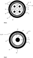
- the lines 2 shown in the example are each designed as data lines and have a central transmission core 4 which is surrounded by a line jacket 6.
- the cable sheath 6 has an outer first layer 8 made of an electrically insulating plastic and a second layer 10, arranged immediately below, made of a semiconducting material.
- the cable jacket 6 is in the examples of Figures 1 and 2 directly on the transmission core 4.
- the line sheath 6 is a line sheath 6 formed by extrusion.
- the two layers 8, 10 are specifically formed by coextrusion.
- the cable sheath 6 is applied to the transmission core 4 in the manner of a hose extrusion.
- the line 2 according to the exemplary variant of FIG 1 is designed as a symmetrical data line with preferably 2 wire pairs in the example.
- a respective pair of wires 12 is used in the data transmission of a symmetrical data signal to transmit on the one hand the signal and on the other hand the inverted signal.
- the respective wire pair 12 is a twisted wire pair.
- a respective wire 14 is formed by a central conductor 16 which is surrounded by an insulating jacket 18 as a wire jacket.
- the cable sheath 6 also has a conductive layer 20, which is formed in particular by a film, specifically a conventional shielding film. It is specifically an aluminum-laminated plastic film. The metal side is in the direction of the second Layer 10 orients and makes electrically conductive contact with it. In an alternative variant, this conductive layer 20 is dispensed with.
- the exemplary variant according to FIG FIG 2 around a coax line in which the transmission core 4 is formed by an inner conductor 22, a dielectric 24 made of insulating plastic material immediately surrounding it, and an outer conductor 26 directly adjacent to the dielectric 24.
- the outer conductor 26 at the same time defines a shielding layer 28.
- this shielding layer 28 has a multilayer structure with a braid 30 and a shielding film 32.
- the shielding film 32 is preferably arranged on the outside, but can alternatively also be arranged on the inside of the braid 30.
- the second semiconducting layer 10 surrounds the shielding layer 28 directly and is designed in particular as an extruded jacket.
- the line 2 As a transmission core, the line 2 only has a twisted pair of wires 12, which is surrounded directly by an intermediate jacket 40. This is a particularly extruded plastic jacket that forms a dielectric 24.
- the intermediate jacket 40 is in turn directly surrounded by the second semiconducting layer 10, which is finally also surrounded by the outer jacket 8.
- the latter is used for electrical insulation, protection against environmental influences or as a spacer.
- a conductive layer 20 can also be formed.
- the structure described here with the intermediate jacket 40 is used to connect conventional unshielded lines, especially data lines, in particular unshielded symmetrical data lines, through a line 2 (symmetrical data line) provided with such a line jacket 6 replace.
- conventional unshielded lines especially data lines, in particular unshielded symmetrical data lines
- line 2 symmetrical data line
- the conventional components for the unshielded data line and the conventional process steps are retained.
- the respective shield of the line 2 is therefore not electrically connected to a reference potential, in particular ground potential, at the component 34 - as is otherwise usual.
- FIG 4 This concept illustrates the FIG 4 . From this it can be seen that the line 2, for example, according to FIG FIG 1 or the FIG 3 is introduced into the component 34, shown only in a greatly simplified manner, through an inlet opening.
- the line sheath 6 is passed through the opening, for example.
- the opening is usually sealed off, for example by a sealing ring, a grommet or by circumferential webs which are pressed into the cable jacket 6.
- the component 34 is, for example, a plug which is used for connection to a consumer. Alternatively, component 34 is directly a consumer. In both cases, the line 2 is passed through the opening of a housing.
- the individual wires 14 are freed from the cable sheath 6 within the component 34 and the respective conductor 16 of the respective wire 14 is stripped and connected at the end to a contact element 36.
- a contact element 36 These are, for example, contact sockets or contact pins that are designed, for example, as crimp contacts. Alternatively, screw contact can also be made.
Claims (15)
- Ligne électrique (2), en particulier ligne de données, avec un noyau de transmission (4) entouré d'un blindage, noyau de transmission (4) étant entouré concentriquement par une gaine de ligne (6), qui comprend une couche extérieure (8) en matière plastique électriquement isolante et une deuxième couche (10) en matériau semi-conducteur disposée en dessous, dans laquelle le noyau de transmission (4) est formé par au moins une paire de noyaux et la au moins une paire de noyaux ne comprend pas de blindage de paire, dans laquelle une gaine intermédiaire (40) est disposée entre le noyau de transmission (4) et la deuxième couche (10), de sorte que la deuxième couche (10) a une distance minimale d'au moins environ 0,5 mm par rapport au noyau de transmission (4).
- Ligne électrique selon la revendication précédente, dans laquelle la deuxième couche (10) est formée par extrusion, en particulier avec la couche extérieure (8) par coextrusion.
- Ligne électrique selon l'une des revendications précédentes, dans laquelle la deuxième couche semi-conductrice (10) a une épaisseur de paroi comprise entre 0,05 et 1,2 mm, en particulier entre 0,1 et 0,3 mm.
- Ligne électrique selon l'une des revendications précédentes, dans laquelle la gaine de ligne (6) sous la deuxième couche (10) comprend une couche conductrice (20), qui s'appuie contre la deuxième couche (10) de manière à établir un contact électrique.
- Ligne électrique selon l'une des revendications 1 à 3, dans laquelle le blindage est formé exclusivement par la deuxième couche (10).
- Ligne électrique selon l'une des revendications précédentes, qui est reliée à au moins une extrémité à un composant électrique (34), dans laquelle le blindage n'est pas en contact électrique avec le composant (34).
- Ligne électrique selon l'une des revendications 1 à 4, dans laquelle au moins une couche de blindage est disposée autour du noyau de transmission (4) en plus de la gaine du ligne (6).
- Ligne électrique selon l'une des revendications précédentes, dans laquelle la résistance spécifique du matériau semi-conducteur est supérieure à 1 Ohm*mm2/m et de préférence supérieure à 10 Ohm*mm2/m.
- Ligne électrique selon la revendication précédente, dans laquelle la résistance respective est inférieure à 1000 Ohm*mm2/m et en particulier inférieure à 100 Ohm*mm2/m.
- Ligne électrique selon l'une des revendications précédentes, dans laquelle le matériau semi-conducteur est un plastique conducteur.
- Ligne électrique selon l'une des revendications précédentes, dans laquelle le matériau semi-conducteur est formé par un plastique isolant, dans lequel sont noyées des particules conductrices, en particulier des particules de carbone, telles que des particules de suie ou des nanoparticules de carbone.
- Ligne électrique selon l'une des revendications précédentes, dans laquelle le matériau semi-conducteur ne comporte pas de particules métalliques et/ou de particules magnétiques, en particulier ferromagnétiques ou magnétisables.
- Ligne électrique selon l'une des revendications précédentes, dans laquelle le noyau de transmission (4) est formé par exactement une paire de noyaux (12), qui est directement entourée par la gaine intermédiaire (40), ladite gaine intermédiaire (40) étant conçue comme une gaine en plastique appliqué par extrusion.
- Ligne électrique selon l'une des revendications précédentes, dans laquelle la distance au noyau de transmission (4) est au maximum de 1,5 mm.
- Ligne électrique selon l'une des deux revendications précédentes, dans laquelle la gaine intermédiaire (40) est constituée d'un matériau isolant de préférence solide, comme par exemple du polypropylène.
Applications Claiming Priority (2)
| Application Number | Priority Date | Filing Date | Title |
|---|---|---|---|
| DE102015221108 | 2015-10-28 | ||
| PCT/EP2016/075999 WO2017072265A1 (fr) | 2015-10-28 | 2016-10-27 | Ligne électrique |
Publications (2)
| Publication Number | Publication Date |
|---|---|
| EP3369099A1 EP3369099A1 (fr) | 2018-09-05 |
| EP3369099B1 true EP3369099B1 (fr) | 2020-12-16 |
Family
ID=57389384
Family Applications (1)
| Application Number | Title | Priority Date | Filing Date |
|---|---|---|---|
| EP16798654.6A Active EP3369099B1 (fr) | 2015-10-28 | 2016-10-27 | Ligne électrique |
Country Status (4)
| Country | Link |
|---|---|
| US (1) | US10325698B2 (fr) |
| EP (1) | EP3369099B1 (fr) |
| CN (1) | CN108352222A (fr) |
| WO (1) | WO2017072265A1 (fr) |
Families Citing this family (1)
| Publication number | Priority date | Publication date | Assignee | Title |
|---|---|---|---|---|
| KR102648667B1 (ko) * | 2019-04-03 | 2024-03-15 | 어플라이드 머티어리얼스, 인코포레이티드 | 스퍼터 증착 소스, 스퍼터 증착 장치, 및 스퍼터 증착 소스에 전력공급하는 방법 |
Family Cites Families (9)
| Publication number | Priority date | Publication date | Assignee | Title |
|---|---|---|---|---|
| US4926008A (en) * | 1989-05-18 | 1990-05-15 | Hewlett-Packard Company | High capacitance cable |
| US5208426A (en) * | 1991-09-03 | 1993-05-04 | W. L. Gore & Associates, Inc. | Shielded electric signal cable having a two-layer semiconductor jacket |
| EP2091089A1 (fr) * | 2008-02-15 | 2009-08-19 | Media-Group GmbH | Dispositif d'alimentation en énergie doté d'un panneau d'énergie et panneau d'énergie |
| US9678027B2 (en) * | 2012-02-29 | 2017-06-13 | Stmicroelectronics S.R.L. | Monitoring device with jumper cable coupling and related methods |
| SG11201406236QA (en) * | 2012-04-27 | 2015-01-29 | Draka Comteq Bv | Electric cable, in particular a data transmission cable, equipped with multi-layer, strip-type screening sheet |
| US10126517B2 (en) * | 2014-06-10 | 2018-11-13 | Corning Optical Communications LLC | Fiber optic cable structured to facilitate accessing an end thereof |
| DE102014214726B3 (de) * | 2014-07-25 | 2015-10-15 | Leoni Kabel Holding Gmbh | Datenkabel für High-Speed Datenübertragungen |
| US9941616B2 (en) * | 2015-02-24 | 2018-04-10 | Thomas & Betts International Llc | Multi-piece jacket for separable connectors |
| CN104751980A (zh) * | 2015-03-30 | 2015-07-01 | 安徽华能电缆集团有限公司 | 一种高压岸电电缆 |
-
2016
- 2016-10-27 WO PCT/EP2016/075999 patent/WO2017072265A1/fr unknown
- 2016-10-27 CN CN201680062440.7A patent/CN108352222A/zh active Pending
- 2016-10-27 EP EP16798654.6A patent/EP3369099B1/fr active Active
-
2018
- 2018-04-17 US US15/954,648 patent/US10325698B2/en active Active
Non-Patent Citations (1)
| Title |
|---|
| None * |
Also Published As
| Publication number | Publication date |
|---|---|
| US10325698B2 (en) | 2019-06-18 |
| US20180233254A1 (en) | 2018-08-16 |
| WO2017072265A1 (fr) | 2017-05-04 |
| EP3369099A1 (fr) | 2018-09-05 |
| CN108352222A (zh) | 2018-07-31 |
Similar Documents
| Publication | Publication Date | Title |
|---|---|---|
| EP3172741B1 (fr) | Câble de données pour transmissions de données à haut débit | |
| DE102007023255B4 (de) | Abgeschirmter Draht | |
| EP1964133A1 (fr) | Cable a trois conducteurs | |
| EP3350813A1 (fr) | Câble de données pour transferts de données haute vitesse | |
| EP3285266B1 (fr) | Câble à toronnage adapté | |
| DE10315609B4 (de) | Datenübertragungskabel | |
| DE102008021204A1 (de) | Halbleitendes Wickelband aus Polytetrafluorethylen | |
| DE102014223119B4 (de) | Datenkabel sowie Verfahren zur Herstellung eines Datenkabels | |
| EP3147913B1 (fr) | Cable de transmission de donnees pouvant etre confectionne | |
| DE102019112742A1 (de) | Koaxialleitung | |
| EP3369099B1 (fr) | Ligne électrique | |
| EP1683235B1 (fr) | Connexion entre un câble coaxial et un connecteur et procédé de réalisation | |
| WO2017076984A1 (fr) | Câble de données ainsi qu'utilisation du câble de données dans un véhicule automobile | |
| EP1946334A1 (fr) | Cable multiconducteur pour la transmission de courants alternatifs de forme rectangulaire | |
| WO2014140223A1 (fr) | Câble électrique ainsi que procédé de fabrication d'un câble électrique | |
| EP2989641B1 (fr) | Câble de données à haut débit | |
| DE202011004949U1 (de) | Elektrische Leitung zum Übertragen von Datensignalen | |
| EP2172946A1 (fr) | Câble électrique destiné à la connexion d'appareils électriques mobiles | |
| EP3886277B1 (fr) | Boîtier à blindage électrique | |
| DE102005022190B3 (de) | Energie-Bus-Kabel | |
| DE102014010777A1 (de) | Hochspannungskabel | |
| EP4092836A1 (fr) | Câble préconfectionné, agencement de connecteur enfichable de câble et connecteur enfichable électrique | |
| WO2003036658A1 (fr) | Conducteur electrique | |
| DE102019118734A1 (de) | Hybridkabel und Leiterplattenanordnung mit einem solchen Hybridkabel | |
| EP1583109A2 (fr) | Câble de commande électrique flexible. |
Legal Events
| Date | Code | Title | Description |
|---|---|---|---|
| STAA | Information on the status of an ep patent application or granted ep patent |
Free format text: STATUS: UNKNOWN |
|
| STAA | Information on the status of an ep patent application or granted ep patent |
Free format text: STATUS: THE INTERNATIONAL PUBLICATION HAS BEEN MADE |
|
| PUAI | Public reference made under article 153(3) epc to a published international application that has entered the european phase |
Free format text: ORIGINAL CODE: 0009012 |
|
| STAA | Information on the status of an ep patent application or granted ep patent |
Free format text: STATUS: REQUEST FOR EXAMINATION WAS MADE |
|
| 17P | Request for examination filed |
Effective date: 20180302 |
|
| AK | Designated contracting states |
Kind code of ref document: A1 Designated state(s): AL AT BE BG CH CY CZ DE DK EE ES FI FR GB GR HR HU IE IS IT LI LT LU LV MC MK MT NL NO PL PT RO RS SE SI SK SM TR |
|
| AX | Request for extension of the european patent |
Extension state: BA ME |
|
| DAV | Request for validation of the european patent (deleted) | ||
| DAX | Request for extension of the european patent (deleted) | ||
| RAP1 | Party data changed (applicant data changed or rights of an application transferred) |
Owner name: LEONI KABEL GMBH |
|
| GRAP | Despatch of communication of intention to grant a patent |
Free format text: ORIGINAL CODE: EPIDOSNIGR1 |
|
| STAA | Information on the status of an ep patent application or granted ep patent |
Free format text: STATUS: GRANT OF PATENT IS INTENDED |
|
| INTG | Intention to grant announced |
Effective date: 20200714 |
|
| GRAS | Grant fee paid |
Free format text: ORIGINAL CODE: EPIDOSNIGR3 |
|
| GRAA | (expected) grant |
Free format text: ORIGINAL CODE: 0009210 |
|
| STAA | Information on the status of an ep patent application or granted ep patent |
Free format text: STATUS: THE PATENT HAS BEEN GRANTED |
|
| AK | Designated contracting states |
Kind code of ref document: B1 Designated state(s): AL AT BE BG CH CY CZ DE DK EE ES FI FR GB GR HR HU IE IS IT LI LT LU LV MC MK MT NL NO PL PT RO RS SE SI SK SM TR |
|
| REG | Reference to a national code |
Ref country code: GB Ref legal event code: FG4D Free format text: NOT ENGLISH |
|
| REG | Reference to a national code |
Ref country code: DE Ref legal event code: R096 Ref document number: 502016012005 Country of ref document: DE |
|
| REG | Reference to a national code |
Ref country code: IE Ref legal event code: FG4D Free format text: LANGUAGE OF EP DOCUMENT: GERMAN |
|
| REG | Reference to a national code |
Ref country code: AT Ref legal event code: REF Ref document number: 1346318 Country of ref document: AT Kind code of ref document: T Effective date: 20210115 |
|
| PG25 | Lapsed in a contracting state [announced via postgrant information from national office to epo] |
Ref country code: NO Free format text: LAPSE BECAUSE OF FAILURE TO SUBMIT A TRANSLATION OF THE DESCRIPTION OR TO PAY THE FEE WITHIN THE PRESCRIBED TIME-LIMIT Effective date: 20210316 Ref country code: RS Free format text: LAPSE BECAUSE OF FAILURE TO SUBMIT A TRANSLATION OF THE DESCRIPTION OR TO PAY THE FEE WITHIN THE PRESCRIBED TIME-LIMIT Effective date: 20201216 Ref country code: FI Free format text: LAPSE BECAUSE OF FAILURE TO SUBMIT A TRANSLATION OF THE DESCRIPTION OR TO PAY THE FEE WITHIN THE PRESCRIBED TIME-LIMIT Effective date: 20201216 Ref country code: GR Free format text: LAPSE BECAUSE OF FAILURE TO SUBMIT A TRANSLATION OF THE DESCRIPTION OR TO PAY THE FEE WITHIN THE PRESCRIBED TIME-LIMIT Effective date: 20210317 |
|
| REG | Reference to a national code |
Ref country code: NL Ref legal event code: MP Effective date: 20201216 |
|
| PG25 | Lapsed in a contracting state [announced via postgrant information from national office to epo] |
Ref country code: SE Free format text: LAPSE BECAUSE OF FAILURE TO SUBMIT A TRANSLATION OF THE DESCRIPTION OR TO PAY THE FEE WITHIN THE PRESCRIBED TIME-LIMIT Effective date: 20201216 Ref country code: LV Free format text: LAPSE BECAUSE OF FAILURE TO SUBMIT A TRANSLATION OF THE DESCRIPTION OR TO PAY THE FEE WITHIN THE PRESCRIBED TIME-LIMIT Effective date: 20201216 Ref country code: BG Free format text: LAPSE BECAUSE OF FAILURE TO SUBMIT A TRANSLATION OF THE DESCRIPTION OR TO PAY THE FEE WITHIN THE PRESCRIBED TIME-LIMIT Effective date: 20210316 |
|
| PG25 | Lapsed in a contracting state [announced via postgrant information from national office to epo] |
Ref country code: NL Free format text: LAPSE BECAUSE OF FAILURE TO SUBMIT A TRANSLATION OF THE DESCRIPTION OR TO PAY THE FEE WITHIN THE PRESCRIBED TIME-LIMIT Effective date: 20201216 Ref country code: HR Free format text: LAPSE BECAUSE OF FAILURE TO SUBMIT A TRANSLATION OF THE DESCRIPTION OR TO PAY THE FEE WITHIN THE PRESCRIBED TIME-LIMIT Effective date: 20201216 |
|
| REG | Reference to a national code |
Ref country code: LT Ref legal event code: MG9D |
|
| PG25 | Lapsed in a contracting state [announced via postgrant information from national office to epo] |
Ref country code: PT Free format text: LAPSE BECAUSE OF FAILURE TO SUBMIT A TRANSLATION OF THE DESCRIPTION OR TO PAY THE FEE WITHIN THE PRESCRIBED TIME-LIMIT Effective date: 20210416 Ref country code: RO Free format text: LAPSE BECAUSE OF FAILURE TO SUBMIT A TRANSLATION OF THE DESCRIPTION OR TO PAY THE FEE WITHIN THE PRESCRIBED TIME-LIMIT Effective date: 20201216 Ref country code: SK Free format text: LAPSE BECAUSE OF FAILURE TO SUBMIT A TRANSLATION OF THE DESCRIPTION OR TO PAY THE FEE WITHIN THE PRESCRIBED TIME-LIMIT Effective date: 20201216 Ref country code: SM Free format text: LAPSE BECAUSE OF FAILURE TO SUBMIT A TRANSLATION OF THE DESCRIPTION OR TO PAY THE FEE WITHIN THE PRESCRIBED TIME-LIMIT Effective date: 20201216 Ref country code: LT Free format text: LAPSE BECAUSE OF FAILURE TO SUBMIT A TRANSLATION OF THE DESCRIPTION OR TO PAY THE FEE WITHIN THE PRESCRIBED TIME-LIMIT Effective date: 20201216 Ref country code: CZ Free format text: LAPSE BECAUSE OF FAILURE TO SUBMIT A TRANSLATION OF THE DESCRIPTION OR TO PAY THE FEE WITHIN THE PRESCRIBED TIME-LIMIT Effective date: 20201216 Ref country code: EE Free format text: LAPSE BECAUSE OF FAILURE TO SUBMIT A TRANSLATION OF THE DESCRIPTION OR TO PAY THE FEE WITHIN THE PRESCRIBED TIME-LIMIT Effective date: 20201216 |
|
| PG25 | Lapsed in a contracting state [announced via postgrant information from national office to epo] |
Ref country code: PL Free format text: LAPSE BECAUSE OF FAILURE TO SUBMIT A TRANSLATION OF THE DESCRIPTION OR TO PAY THE FEE WITHIN THE PRESCRIBED TIME-LIMIT Effective date: 20201216 |
|
| REG | Reference to a national code |
Ref country code: DE Ref legal event code: R097 Ref document number: 502016012005 Country of ref document: DE |
|
| PG25 | Lapsed in a contracting state [announced via postgrant information from national office to epo] |
Ref country code: IS Free format text: LAPSE BECAUSE OF FAILURE TO SUBMIT A TRANSLATION OF THE DESCRIPTION OR TO PAY THE FEE WITHIN THE PRESCRIBED TIME-LIMIT Effective date: 20210416 |
|
| PLBE | No opposition filed within time limit |
Free format text: ORIGINAL CODE: 0009261 |
|
| STAA | Information on the status of an ep patent application or granted ep patent |
Free format text: STATUS: NO OPPOSITION FILED WITHIN TIME LIMIT |
|
| PG25 | Lapsed in a contracting state [announced via postgrant information from national office to epo] |
Ref country code: IT Free format text: LAPSE BECAUSE OF FAILURE TO SUBMIT A TRANSLATION OF THE DESCRIPTION OR TO PAY THE FEE WITHIN THE PRESCRIBED TIME-LIMIT Effective date: 20201216 Ref country code: AL Free format text: LAPSE BECAUSE OF FAILURE TO SUBMIT A TRANSLATION OF THE DESCRIPTION OR TO PAY THE FEE WITHIN THE PRESCRIBED TIME-LIMIT Effective date: 20201216 |
|
| 26N | No opposition filed |
Effective date: 20210917 |
|
| PG25 | Lapsed in a contracting state [announced via postgrant information from national office to epo] |
Ref country code: DK Free format text: LAPSE BECAUSE OF FAILURE TO SUBMIT A TRANSLATION OF THE DESCRIPTION OR TO PAY THE FEE WITHIN THE PRESCRIBED TIME-LIMIT Effective date: 20201216 |
|
| PG25 | Lapsed in a contracting state [announced via postgrant information from national office to epo] |
Ref country code: ES Free format text: LAPSE BECAUSE OF FAILURE TO SUBMIT A TRANSLATION OF THE DESCRIPTION OR TO PAY THE FEE WITHIN THE PRESCRIBED TIME-LIMIT Effective date: 20201216 |
|
| PG25 | Lapsed in a contracting state [announced via postgrant information from national office to epo] |
Ref country code: SI Free format text: LAPSE BECAUSE OF FAILURE TO SUBMIT A TRANSLATION OF THE DESCRIPTION OR TO PAY THE FEE WITHIN THE PRESCRIBED TIME-LIMIT Effective date: 20201216 |
|
| REG | Reference to a national code |
Ref country code: CH Ref legal event code: PL |
|
| PG25 | Lapsed in a contracting state [announced via postgrant information from national office to epo] |
Ref country code: IS Free format text: LAPSE BECAUSE OF FAILURE TO SUBMIT A TRANSLATION OF THE DESCRIPTION OR TO PAY THE FEE WITHIN THE PRESCRIBED TIME-LIMIT Effective date: 20210416 |
|
| REG | Reference to a national code |
Ref country code: BE Ref legal event code: MM Effective date: 20211031 |
|
| GBPC | Gb: european patent ceased through non-payment of renewal fee |
Effective date: 20211027 |
|
| PG25 | Lapsed in a contracting state [announced via postgrant information from national office to epo] |
Ref country code: MC Free format text: LAPSE BECAUSE OF FAILURE TO SUBMIT A TRANSLATION OF THE DESCRIPTION OR TO PAY THE FEE WITHIN THE PRESCRIBED TIME-LIMIT Effective date: 20201216 |
|
| PG25 | Lapsed in a contracting state [announced via postgrant information from national office to epo] |
Ref country code: LU Free format text: LAPSE BECAUSE OF NON-PAYMENT OF DUE FEES Effective date: 20211027 Ref country code: GB Free format text: LAPSE BECAUSE OF NON-PAYMENT OF DUE FEES Effective date: 20211027 Ref country code: BE Free format text: LAPSE BECAUSE OF NON-PAYMENT OF DUE FEES Effective date: 20211031 |
|
| PG25 | Lapsed in a contracting state [announced via postgrant information from national office to epo] |
Ref country code: LI Free format text: LAPSE BECAUSE OF NON-PAYMENT OF DUE FEES Effective date: 20211031 Ref country code: CH Free format text: LAPSE BECAUSE OF NON-PAYMENT OF DUE FEES Effective date: 20211031 |
|
| PG25 | Lapsed in a contracting state [announced via postgrant information from national office to epo] |
Ref country code: FR Free format text: LAPSE BECAUSE OF NON-PAYMENT OF DUE FEES Effective date: 20211031 |
|
| PG25 | Lapsed in a contracting state [announced via postgrant information from national office to epo] |
Ref country code: IE Free format text: LAPSE BECAUSE OF NON-PAYMENT OF DUE FEES Effective date: 20211027 |
|
| REG | Reference to a national code |
Ref country code: AT Ref legal event code: MM01 Ref document number: 1346318 Country of ref document: AT Kind code of ref document: T Effective date: 20211027 |
|
| PG25 | Lapsed in a contracting state [announced via postgrant information from national office to epo] |
Ref country code: AT Free format text: LAPSE BECAUSE OF NON-PAYMENT OF DUE FEES Effective date: 20211027 |
|
| PG25 | Lapsed in a contracting state [announced via postgrant information from national office to epo] |
Ref country code: HU Free format text: LAPSE BECAUSE OF FAILURE TO SUBMIT A TRANSLATION OF THE DESCRIPTION OR TO PAY THE FEE WITHIN THE PRESCRIBED TIME-LIMIT; INVALID AB INITIO Effective date: 20161027 |
|
| P01 | Opt-out of the competence of the unified patent court (upc) registered |
Effective date: 20230505 |
|
| PG25 | Lapsed in a contracting state [announced via postgrant information from national office to epo] |
Ref country code: CY Free format text: LAPSE BECAUSE OF FAILURE TO SUBMIT A TRANSLATION OF THE DESCRIPTION OR TO PAY THE FEE WITHIN THE PRESCRIBED TIME-LIMIT Effective date: 20201216 |
|
| PGFP | Annual fee paid to national office [announced via postgrant information from national office to epo] |
Ref country code: DE Payment date: 20231018 Year of fee payment: 8 |
|
| PG25 | Lapsed in a contracting state [announced via postgrant information from national office to epo] |
Ref country code: MK Free format text: LAPSE BECAUSE OF FAILURE TO SUBMIT A TRANSLATION OF THE DESCRIPTION OR TO PAY THE FEE WITHIN THE PRESCRIBED TIME-LIMIT Effective date: 20201216 |