EP3367570B1 - Temperature compensated crystal oscillator - Google Patents
Temperature compensated crystal oscillator Download PDFInfo
- Publication number
- EP3367570B1 EP3367570B1 EP18158193.5A EP18158193A EP3367570B1 EP 3367570 B1 EP3367570 B1 EP 3367570B1 EP 18158193 A EP18158193 A EP 18158193A EP 3367570 B1 EP3367570 B1 EP 3367570B1
- Authority
- EP
- European Patent Office
- Prior art keywords
- temperature
- temperature compensation
- substantially higher
- crystal oscillator
- function
- Prior art date
- Legal status (The legal status is an assumption and is not a legal conclusion. Google has not performed a legal analysis and makes no representation as to the accuracy of the status listed.)
- Active
Links
Images


Classifications
-
- H—ELECTRICITY
- H03—ELECTRONIC CIRCUITRY
- H03B—GENERATION OF OSCILLATIONS, DIRECTLY OR BY FREQUENCY-CHANGING, BY CIRCUITS EMPLOYING ACTIVE ELEMENTS WHICH OPERATE IN A NON-SWITCHING MANNER; GENERATION OF NOISE BY SUCH CIRCUITS
- H03B5/00—Generation of oscillations using amplifier with regenerative feedback from output to input
- H03B5/02—Details
- H03B5/04—Modifications of generator to compensate for variations in physical values, e.g. power supply, load, temperature
-
- H—ELECTRICITY
- H03—ELECTRONIC CIRCUITRY
- H03B—GENERATION OF OSCILLATIONS, DIRECTLY OR BY FREQUENCY-CHANGING, BY CIRCUITS EMPLOYING ACTIVE ELEMENTS WHICH OPERATE IN A NON-SWITCHING MANNER; GENERATION OF NOISE BY SUCH CIRCUITS
- H03B5/00—Generation of oscillations using amplifier with regenerative feedback from output to input
- H03B5/30—Generation of oscillations using amplifier with regenerative feedback from output to input with frequency-determining element being electromechanical resonator
- H03B5/32—Generation of oscillations using amplifier with regenerative feedback from output to input with frequency-determining element being electromechanical resonator being a piezoelectric resonator
-
- H—ELECTRICITY
- H03—ELECTRONIC CIRCUITRY
- H03L—AUTOMATIC CONTROL, STARTING, SYNCHRONISATION OR STABILISATION OF GENERATORS OF ELECTRONIC OSCILLATIONS OR PULSES
- H03L1/00—Stabilisation of generator output against variations of physical values, e.g. power supply
- H03L1/02—Stabilisation of generator output against variations of physical values, e.g. power supply against variations of temperature only
- H03L1/022—Stabilisation of generator output against variations of physical values, e.g. power supply against variations of temperature only by indirect stabilisation, i.e. by generating an electrical correction signal which is a function of the temperature
- H03L1/027—Stabilisation of generator output against variations of physical values, e.g. power supply against variations of temperature only by indirect stabilisation, i.e. by generating an electrical correction signal which is a function of the temperature by using frequency conversion means which is variable with temperature, e.g. mixer, frequency divider, pulse add/subtract logic circuit
-
- H—ELECTRICITY
- H03—ELECTRONIC CIRCUITRY
- H03L—AUTOMATIC CONTROL, STARTING, SYNCHRONISATION OR STABILISATION OF GENERATORS OF ELECTRONIC OSCILLATIONS OR PULSES
- H03L1/00—Stabilisation of generator output against variations of physical values, e.g. power supply
- H03L1/02—Stabilisation of generator output against variations of physical values, e.g. power supply against variations of temperature only
- H03L1/028—Stabilisation of generator output against variations of physical values, e.g. power supply against variations of temperature only of generators comprising piezoelectric resonators
-
- H—ELECTRICITY
- H03—ELECTRONIC CIRCUITRY
- H03L—AUTOMATIC CONTROL, STARTING, SYNCHRONISATION OR STABILISATION OF GENERATORS OF ELECTRONIC OSCILLATIONS OR PULSES
- H03L1/00—Stabilisation of generator output against variations of physical values, e.g. power supply
- H03L1/02—Stabilisation of generator output against variations of physical values, e.g. power supply against variations of temperature only
- H03L1/04—Constructional details for maintaining temperature constant
-
- H—ELECTRICITY
- H03—ELECTRONIC CIRCUITRY
- H03L—AUTOMATIC CONTROL, STARTING, SYNCHRONISATION OR STABILISATION OF GENERATORS OF ELECTRONIC OSCILLATIONS OR PULSES
- H03L7/00—Automatic control of frequency or phase; Synchronisation
- H03L7/06—Automatic control of frequency or phase; Synchronisation using a reference signal applied to a frequency- or phase-locked loop
- H03L7/08—Details of the phase-locked loop
- H03L7/099—Details of the phase-locked loop concerning mainly the controlled oscillator of the loop
Definitions
- the present invention relates to Temperature Compensated Crystal Oscillators (TCXOs) wherein the residual frequency instability is reduced by applying an additional temperature compensation signal, generated as a single, or a combination of two or more, suitable non-linear functions of a signal carrying temperature information.
- TCXOs Temperature Compensated Crystal Oscillators
- TCXO Voltage Controlled Crystal Oscillator
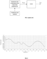
- the VCXO is a tunable circuit arranged to produce an output signal of required frequency F OUT .
- the resonant frequency of the crystal resonator deployed as part of the VCXO circuit is temperature-dependent.
- a Temperature Compensation Function Generator circuit is arranged to produce temperature compensating voltage V COMP , and the latter is applied to the VCXO to correct the output frequency.
- the compensating voltage is produced as a function of the temperature sensor output signal, and the function is tailored so that, in conjunction with the VCXO's frequency versus temperature characteristic, the application of the V COMP voltage reduces the output frequency F OUT instability.
- the frequency versus temperature characteristic of the VCXO is usually approximated as a polynomial function, and the compensating voltage V COMP is generated by the Temperature Compensation Function Generator as a polynomial function to suit the characteristic of the VCXO.
- the residual frequency versus temperature error curve of an analog TCXO cannot be easily defined by a simple mathematical expression such as a polynomial function.
- the shape of the error curve is different for every TCXO sample; in particular, the position, magnitude, shape, and number of non-linearities in the frequency error curve with respect to temperature are unique for every TCXO device.
- These non-linearities are a result of interaction between the crystal resonator characteristic non-linearities and oscillator component characteristic non-linearities. Shown in Fig. 2 and Fig. 2a are examples of two real-life TCXO frequency versus temperature error curves.
- Another known approach is piecewise residual frequency error reduction, whereby the residual frequency versus temperature curve is divided into two or more segments, and each segment is approximated by its own analog function generator that operates over the temperature range relating to that segment.
- This approach is often not practicable in terms of its hardware implementation, and frequency jumps at the segment boundaries are difficult to eliminate.
- WO2015/193539 and US6002291 disclose temperature compensation schemes for primary compensation.
- US2014/0337261 discloses the use of an Artificial Neural Network for primary or secondary temperature compensation.
- EP1209812 discloses predistorting an input signal for a tunable circuit, such as an oscillator circuit or a filter circuit, so that an output of the tunable circuit is substantially corrected for non-linearities in the tuning of the tunable circuit.
- a tunable circuit such as an oscillator circuit or a filter circuit
- GB2363269 discloses a temperature-compensated crystal oscillator.
- the present invention offers a useful way of reducing the temperature compensation frequency errors, whereby an additional temperature compensation signal ("secondary compensation” signal, or “post-compensation” signal) is generated as either a single, or a combination of two or more, signals generated as suitable non-linear functions that are active over the intended compensation temperature range.
- secondary compensation signal or "post-compensation” signal
- the invention provides a practicable temperature compensation technique that makes it possible to further reduce frequency instability in Temperature Compensated Crystal Oscillators (TCXOs).
- TCXOs Temperature Compensated Crystal Oscillators
- a secondary temperature compensation signal is generated as either a single, or as a combination of two or more, analog signals generated as suitable non-linear functions operating over the intended compensation temperature range, and the thus formed secondary temperature compensation signal is applied to the VCXO circuit to further improve the TCXO's frequency stability.
- the suitable non-linear functions used to generate the secondary temperature compensation signal can be any one or more functions that satisfy the following requirements:
- the last requirement allows to shape the secondary (post-compensation) signal to match the targeted TCXO's primary compensation residual frequency error curve shape as closely as possible.
- a region approximating a plateau or "a plateau region” means a region of the function curve that exhibits a linear asymptotic approach to a zero slope (horizontal) line.
- the "substantially higher slope region” is a region of the function curve having a slope that is substantially higher than the slope in the plateau region.
- sigmoid functions are suitable for implementing the post-compensation technique, as sigmoid functions satisfy the aforementioned requirements.
- a sigmoid function is bounded by a pair of horizontal asymptotes and first derivative (i.e., slope) of a sigmoid function is bell shaped, a sigmoid function has two regions approximating plateaux and a region where the function slope value is substantially higher than that in the plateauing regions.
- the magnitude, slope, and position of the said single, or a number of, generated function signals are adjusted for every TCXO device so that the post-compensation signal, formed as a combination of the generated functions, is optimized for the shape of the particular TCXO's primary compensation residual frequency error curve.
- the functions chosen to be used for generating the one or more signals to form the secondary temperature compensation signal are such that the horizontal position of the substantially higher slope region, the slope value in the substantially higher slope region, and the function value change magnitude over the substantially higher slope region are adjustable independently from each other, although functions with interactions between these parameters can be also deployed, as the interactions can be accounted for when optimal parameter values are being determined.
- the horizontal position of the generated functions is adjustable to cover the compensation temperature range of a given TCXO population.
- the horizontal position of the generated functions is arranged to be adjustable within the temperature range from -40°C to +85°C; in other embodiments, a wider horizontal position adjustment range from -55°C to +105°C is required; in yet other embodiments, an even wider horizontal position adjustment range from -55°C to +125°C is required.
- a horizontal position adjustment range different than those mentioned above may be required to suit the compensation temperature range specified for a given TCXO population.
- the magnitude of the generated functions is adjustable to cover the possible magnitude range of TCXOs' primary compensation residual frequency error.
- Contemporary TCXOs exhibit primary compensation residual frequency instability ranging from ⁇ 100PPB maximum, to about ⁇ 2.5PPM maximum over the intended compensation temperature range.
- the magnitude of function signals generated according to the present invention is adjustable within a range of about ⁇ 100PPB; in other embodiments, the required function magnitude adjustment range is wider and extends to ⁇ 0.5PPM; in yet other embodiments, an even wider range of ⁇ 2.5PPM is required.
- a function magnitude adjustment range different than those mentioned above may be required to post-compensate the primary compensation residual frequency errors of a given TCXO population.
- an Arctangent (arctan) function also belonging to the sigmoid set of functions, may be more suitable. No matter which specific function is chosen, it must satisfy the requirements listed above.
- the invention comprises an auxiliary integrated circuit such as defined in claim 8.
- any one or more of the aforementioned adjustments of a horizontal position of the substantially higher slope region, of a slope value in the substantially higher slope region, and of a function value change magnitude over the substantially higher slope region can be effected indirectly and as a consequence of adjusting other function parameters.
- adjusting the horizontal position of a region where the substantially higher slope region and the plateau region are connecting will have the effect of effectively adjusting the horizontal position of the substantially higher slope region.
- adjusting the relative horizontal positions of, or spacing between, regions where the substantially higher slope region is connecting to each of the two plateau regions in a sigmoid function will have the effect of effectively adjusting the slope of the higher slope region.
- adjusting the magnitude of the function change over another region may have the consequential effect of adjusting the function value change magnitude over the substantially higher slope region.
- any one or more of the function adjustments of a horizontal position of the substantially higher slope region, of a slope value in the substantially higher slope region, and of a function value change magnitude over the substantially higher slope region can be implemented as either direct, or indirect adjustments of these function parameters.
- references to adjusting or adjustment of the horizontal position of the substantially higher slope region, slope value in the substantially higher slope region, and function value change magnitude over the substantially higher slope region should be understood accordingly.
- post-compensation signals are generated and applied to the VCXO (the latter comprises part of a TCXO, as shown in Fig. 1 (prior art)).
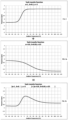
- the post-compensation signal is generated as one, or a combination of multiple, signals, each such signal formed as a function satisfying the aforementioned requirements, such as, for example, the hyperbolic tangent Tanh function.
- the hyperbolic tangent function Tanh generates a smooth, rounded and bounded analog curve which can be used effectively when reducing TCXOs' primary compensation residual frequency errors.
- An example plot of a Tanh function is shown in Fig. 3 .
- Tanh function signals can be readily generated using bipolar electronic circuits, as a bipolar differential transistor pair has a Tanh response.
- Tanh function can be mathematically expressed in a number of different ways.
- FIG. 4, 4a and 4b present an example of two signals generated as Tanh functions of temperature ( Fig. 4 and 4a ), and the result of combining these two functions to form a secondary temperature compensation signal suitable to correct primary compensation residual errors in a TCXO ( Fig. 4b ).
- the two Tanh signals are generated using different sets of "a", "b", and "c" coefficients.
- the third plot shows the combination (sum) of the two Tanh functions.
- Tanh signals voltage or currents
- the magnitude i.e., the function value change magnitude over the substantially higher slope region
- the slope is set by adjusting the value of coefficient "b”
- the horizontal position is set by adjusting the value of coefficient "c”.
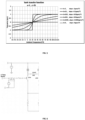
- FIG. 6 An example of an electronic circuit that generates a Tanh voltage is shown in Fig. 6 .
- a signal carrying temperature information temperature sensor output voltage "V Temp Sensor" is used as one of the input voltages and the Tanh function argument.
- the value of the "RGAIN" resistor connected between emitters of transistors QP26 and QP28 determines the magnitude of the generated Tanh function (corresponds to coefficient "a” in the equation above); the value of the resistor "RSLOPE” connected between emitters of transistors QN1 and QN2 determines the slope of the generated Tanh function (corresponds to coefficient "b” in the equation above); another circuit input - at terminal "V Set Inflection" - accepts a voltage that determines the horizontal position of the generated Tanh function curve (corresponds to coefficient "c” in the equation above).
- the graph shown in Fig. 7 illustrates how the horizontal position, slope and magnitude of the Tanh function generated by the circuit shown in Fig. 6 change when the "V Set Inflection" voltage, "RSLOPE” resistor value and “RGAIN” resistor values are changed.
- Fig. 6 shows an implementation example of a circuit generating a hyperbolic tangent Tanh voltage
- the Tanh function generating circuitry is not limited to the example shown in Fig. 6 , and a person skilled in the art of electronic circuit design will be able to come up with alternative circuits to generate a Tanh function signal.
- the temperature compensation technique of the present invention has a number of advantages over digital post-compensation or over piecewise analog post-compensation, such as, -
- the secondary temperature compensation technique can be implemented as part of a complete TCXO integrated circuit (IC), or as a stand-alone auxiliary IC that allows to use the secondary temperature compensation technique to improve the frequency stability of prior art TCXOs, such as, for example, the primary compensated TCXO shown in Fig. 1 (prior art).
- IC TCXO integrated circuit
- FIG. 8 A structure example of a complete TCXO IC deploying the compensation technique of the present invention is shown in Fig. 8 .
- the V COMP voltage (3) generated by the primary Temperature Compensation Function Generator (2) (as in Fig. 1 (prior art)) is added to a post-compensation voltage V PCOMP (5) generated by the Post-Compensation Voltage Generator (4) as per the present invention, and the sum of the voltages V COMP and V PCOMP is applied to compensate the VCXO and thus achieve higher stability of frequency F OUT .
- the invention is illustrated herein by showing how it can be used to effect additional temperature compensation ("post-compensation") in TCXO devices where primary temperature compensation is done by other techniques (such as, for example, a polynomial function), the present invention can be used, without deviating from its concept, to form the primary temperature compensation signal too, if the frequency versus temperature characteristic of the uncompensated oscillator lends itself to a close enough approximation by either a single, or by a combination of several, Tanh functions, or any other functions satisfying the aforementioned requirements.
- the signals generated as Tanh functions, or as any other functions satisfying the aforementioned requirements, are generated by analog circuits (such as, for example, the circuit shown in Fig. 6 ).
- the signals are generated as functions of a signal carrying temperature information, which can be an analog signal produced, for example, by an analog temperature sensor.
- all of the horizontal position of the higher slope region, slope value in the higher slope region, and the function value change magnitude over the higher slope region are adjustable.
- any one only or two only of the horizontal position of the higher slope region, slope value in the higher slope region, and function value change magnitude over the higher slope region may be adjustable.
- a stand-alone auxiliary IC can be implemented and used to post-compensate prior art TCXOs.
- the structure of such an auxiliary IC is shown in Fig. 9 .
- the "CONTROL VOLTAGE" that is usually applied to the "VCO” input of the "PRIOR ART TCXO”
- the post-compensation voltage V PCOMP (5) generated as per the techniques of the present invention, for example as a single, or a combination of a two or more, Tanh function voltages.
- the output of the summing block is the new control signal that is now applied to the "VCO" input of the "PRIOR ART TCXO" to post-compensate the "PRIOR ART TCXO".
Landscapes
- Oscillators With Electromechanical Resonators (AREA)
- Stabilization Of Oscillater, Synchronisation, Frequency Synthesizers (AREA)
- Engineering & Computer Science (AREA)
- Mechanical Engineering (AREA)
- Physics & Mathematics (AREA)
- General Physics & Mathematics (AREA)
Applications Claiming Priority (1)
| Application Number | Priority Date | Filing Date | Title |
|---|---|---|---|
| NZ72945317 | 2017-02-23 |
Publications (3)
| Publication Number | Publication Date |
|---|---|
| EP3367570A1 EP3367570A1 (en) | 2018-08-29 |
| EP3367570C0 EP3367570C0 (en) | 2025-04-16 |
| EP3367570B1 true EP3367570B1 (en) | 2025-04-16 |
Family
ID=61256847
Family Applications (2)
| Application Number | Title | Priority Date | Filing Date |
|---|---|---|---|
| EP18158197.6A Active EP3367571B1 (en) | 2017-02-23 | 2018-02-22 | Voltage controlled oscillator |
| EP18158193.5A Active EP3367570B1 (en) | 2017-02-23 | 2018-02-22 | Temperature compensated crystal oscillator |
Family Applications Before (1)
| Application Number | Title | Priority Date | Filing Date |
|---|---|---|---|
| EP18158197.6A Active EP3367571B1 (en) | 2017-02-23 | 2018-02-22 | Voltage controlled oscillator |
Country Status (3)
| Country | Link |
|---|---|
| US (2) | US10790831B2 (enExample) |
| EP (2) | EP3367571B1 (enExample) |
| JP (2) | JP7254446B2 (enExample) |
Families Citing this family (7)
| Publication number | Priority date | Publication date | Assignee | Title |
|---|---|---|---|---|
| JP6798121B2 (ja) | 2016-03-18 | 2020-12-09 | セイコーエプソン株式会社 | 発振器、電子機器および移動体 |
| JP7035604B2 (ja) * | 2017-03-23 | 2022-03-15 | セイコーエプソン株式会社 | 温度補償型発振器、電子機器および移動体 |
| JP7190331B2 (ja) * | 2018-11-05 | 2022-12-15 | 旭化成エレクトロニクス株式会社 | 温度補償電圧生成回路、発振モジュール、及び、システム |
| CN109543320B (zh) * | 2018-11-29 | 2023-04-18 | 西安电子科技大学 | 一种进行at切温补晶振的应力补偿膜设计方法 |
| US11018625B1 (en) * | 2020-02-28 | 2021-05-25 | Nxp B.V. | Frequency reference generator |
| US10903790B1 (en) | 2020-05-28 | 2021-01-26 | Nxp B.V. | Frequency reference generator |
| JP2023103894A (ja) | 2022-01-14 | 2023-07-27 | 旭化成エレクトロニクス株式会社 | 発振回路および発振回路の温度補償方法 |
Citations (2)
| Publication number | Priority date | Publication date | Assignee | Title |
|---|---|---|---|---|
| EP1209812A1 (en) * | 2000-11-21 | 2002-05-29 | C-Mac Quartz Crystals Limited | A method and apparatus for generating an input signal for a parameter sensitive circuit |
| US6603364B2 (en) * | 2000-03-17 | 2003-08-05 | Asahi Kasei Microsystems Co., Ltd. | Temperature-compensated crystal oscillator and method of temperature compensation |
Family Cites Families (11)
| Publication number | Priority date | Publication date | Assignee | Title |
|---|---|---|---|---|
| FR2758919B1 (fr) * | 1997-01-24 | 1999-04-16 | Sgs Thomson Microelectronics | Circuit de modulation de frequence d'un oscillateur a quartz |
| US6002291A (en) * | 1998-02-27 | 1999-12-14 | Analog Devices, Inc. | Cubic type temperature function generator with adjustable parameters |
| US7161440B2 (en) * | 2003-12-11 | 2007-01-09 | Seiko Epson Corporation | Temperature compensation circuit |
| JP5119826B2 (ja) * | 2007-09-25 | 2013-01-16 | セイコーエプソン株式会社 | 補償電圧回路及び温度補償型圧電発振器 |
| US9092729B2 (en) * | 2011-08-11 | 2015-07-28 | Greenray Industries, Inc. | Trim effect compensation using an artificial neural network |
| JP2013211654A (ja) * | 2012-03-30 | 2013-10-10 | Seiko Epson Corp | 発振器、電子機器及び発振器の温度補償方法 |
| JP5966577B2 (ja) | 2012-05-08 | 2016-08-10 | セイコーエプソン株式会社 | 温度補償回路、回路装置、電子機器及び調整方法 |
| US8643444B2 (en) * | 2012-06-04 | 2014-02-04 | Broadcom Corporation | Common reference crystal systems |
| JP6414382B2 (ja) | 2013-12-25 | 2018-10-31 | セイコーエプソン株式会社 | 発振回路、発振器、電子機器及び移動体 |
| FI20145586A7 (fi) * | 2014-06-18 | 2015-12-19 | Micro Analog Syst Oy | Menetelmä ja integroitu piiri oskillaattorin lämpötilakompensointia varten sekä lämpötilakompensoitu oskillaattoriyksikkö |
| JP6561482B2 (ja) | 2015-02-04 | 2019-08-21 | セイコーエプソン株式会社 | 発振器、電子機器及び移動体 |
-
2018
- 2018-02-22 EP EP18158197.6A patent/EP3367571B1/en active Active
- 2018-02-22 EP EP18158193.5A patent/EP3367570B1/en active Active
- 2018-02-23 JP JP2018030921A patent/JP7254446B2/ja active Active
- 2018-02-23 JP JP2018030913A patent/JP7336830B2/ja active Active
- 2018-02-23 US US15/903,178 patent/US10790831B2/en active Active
- 2018-02-23 US US15/903,226 patent/US10778232B2/en active Active
Patent Citations (2)
| Publication number | Priority date | Publication date | Assignee | Title |
|---|---|---|---|---|
| US6603364B2 (en) * | 2000-03-17 | 2003-08-05 | Asahi Kasei Microsystems Co., Ltd. | Temperature-compensated crystal oscillator and method of temperature compensation |
| EP1209812A1 (en) * | 2000-11-21 | 2002-05-29 | C-Mac Quartz Crystals Limited | A method and apparatus for generating an input signal for a parameter sensitive circuit |
Also Published As
| Publication number | Publication date |
|---|---|
| JP2018137755A (ja) | 2018-08-30 |
| US10778232B2 (en) | 2020-09-15 |
| EP3367570C0 (en) | 2025-04-16 |
| EP3367571A1 (en) | 2018-08-29 |
| US10790831B2 (en) | 2020-09-29 |
| EP3367571B1 (en) | 2025-04-16 |
| EP3367570A1 (en) | 2018-08-29 |
| EP3367571C0 (en) | 2025-04-16 |
| JP7336830B2 (ja) | 2023-09-01 |
| US20180241401A1 (en) | 2018-08-23 |
| JP7254446B2 (ja) | 2023-04-10 |
| US20180375524A1 (en) | 2018-12-27 |
| JP2018137754A (ja) | 2018-08-30 |
Similar Documents
| Publication | Publication Date | Title |
|---|---|---|
| EP3367570B1 (en) | Temperature compensated crystal oscillator | |
| US6294962B1 (en) | Circuit(s), architecture and method(s) for operating and/or tuning a ring oscillator | |
| KR100543680B1 (ko) | 에이지씨 및 온-칩 튜닝을 가지는 수정 발진기 | |
| US10461693B2 (en) | Circuit device, oscillator, electronic apparatus, and moving object | |
| US10256824B2 (en) | D/A converter, circuit device, oscillator, electronic apparatus and moving object | |
| US6404294B1 (en) | Voltage control oscillator (VCO) with automatic gain control | |
| US5691671A (en) | Method and apparatus for a crystal oscillator using piecewise linear odd symmetry temperature compensation | |
| EP0401919B1 (en) | Temperature controlled crystal oscillator circuit | |
| US10218375B2 (en) | Circuit device, oscillator, electronic apparatus, and vehicle | |
| US6549055B2 (en) | Method and apparatus for generating an input signal for a parameter sensitive circuit | |
| US6570461B1 (en) | Trim effect compensation circuit | |
| WO2021205695A1 (ja) | 可変容量素子及びそれを備えた発振器 | |
| KR100515032B1 (ko) | 전압 제어 발진기 | |
| JP2002217643A (ja) | 水晶発振器の温度補償電圧発生回路 | |
| US20250167733A1 (en) | Electronic oscillator with independent controls of variable capacities | |
| JP5918546B2 (ja) | 温度補償型水晶発振器 | |
| JP2008535428A (ja) | 同調制御装置 | |
| US20060001469A1 (en) | Using active circuits to compensate for resistance variations in embedded poly resistors | |
| JPH11346116A (ja) | 温度補償圧電発振器 | |
| JPS6260843B2 (enExample) | ||
| GB2425007A (en) | Variable reactance tuning for a resonant circuit | |
| JPH09232868A (ja) | 温度補償水晶発振器 |
Legal Events
| Date | Code | Title | Description |
|---|---|---|---|
| PUAI | Public reference made under article 153(3) epc to a published international application that has entered the european phase |
Free format text: ORIGINAL CODE: 0009012 |
|
| STAA | Information on the status of an ep patent application or granted ep patent |
Free format text: STATUS: THE APPLICATION HAS BEEN PUBLISHED |
|
| AK | Designated contracting states |
Kind code of ref document: A1 Designated state(s): AL AT BE BG CH CY CZ DE DK EE ES FI FR GB GR HR HU IE IS IT LI LT LU LV MC MK MT NL NO PL PT RO RS SE SI SK SM TR |
|
| AX | Request for extension of the european patent |
Extension state: BA ME |
|
| STAA | Information on the status of an ep patent application or granted ep patent |
Free format text: STATUS: REQUEST FOR EXAMINATION WAS MADE |
|
| 17P | Request for examination filed |
Effective date: 20190226 |
|
| RBV | Designated contracting states (corrected) |
Designated state(s): AL AT BE BG CH CY CZ DE DK EE ES FI FR GB GR HR HU IE IS IT LI LT LU LV MC MK MT NL NO PL PT RO RS SE SI SK SM TR |
|
| STAA | Information on the status of an ep patent application or granted ep patent |
Free format text: STATUS: EXAMINATION IS IN PROGRESS |
|
| 17Q | First examination report despatched |
Effective date: 20211006 |
|
| GRAP | Despatch of communication of intention to grant a patent |
Free format text: ORIGINAL CODE: EPIDOSNIGR1 |
|
| STAA | Information on the status of an ep patent application or granted ep patent |
Free format text: STATUS: GRANT OF PATENT IS INTENDED |
|
| RIC1 | Information provided on ipc code assigned before grant |
Ipc: H03L 7/099 20060101ALI20241016BHEP Ipc: H03L 1/02 20060101AFI20241016BHEP |
|
| INTG | Intention to grant announced |
Effective date: 20241115 |
|
| GRAS | Grant fee paid |
Free format text: ORIGINAL CODE: EPIDOSNIGR3 |
|
| GRAA | (expected) grant |
Free format text: ORIGINAL CODE: 0009210 |
|
| STAA | Information on the status of an ep patent application or granted ep patent |
Free format text: STATUS: THE PATENT HAS BEEN GRANTED |
|
| AK | Designated contracting states |
Kind code of ref document: B1 Designated state(s): AL AT BE BG CH CY CZ DE DK EE ES FI FR GB GR HR HU IE IS IT LI LT LU LV MC MK MT NL NO PL PT RO RS SE SI SK SM TR |
|
| REG | Reference to a national code |
Ref country code: GB Ref legal event code: FG4D |
|
| REG | Reference to a national code |
Ref country code: CH Ref legal event code: EP |
|
| REG | Reference to a national code |
Ref country code: IE Ref legal event code: FG4D |
|
| U01 | Request for unitary effect filed |
Effective date: 20250422 |
|
| U07 | Unitary effect registered |
Designated state(s): AT BE BG DE DK EE FI FR IT LT LU LV MT NL PT RO SE SI Effective date: 20250425 |
|
| PG25 | Lapsed in a contracting state [announced via postgrant information from national office to epo] |
Ref country code: ES Free format text: LAPSE BECAUSE OF FAILURE TO SUBMIT A TRANSLATION OF THE DESCRIPTION OR TO PAY THE FEE WITHIN THE PRESCRIBED TIME-LIMIT Effective date: 20250416 |
|
| PG25 | Lapsed in a contracting state [announced via postgrant information from national office to epo] |
Ref country code: GR Free format text: LAPSE BECAUSE OF FAILURE TO SUBMIT A TRANSLATION OF THE DESCRIPTION OR TO PAY THE FEE WITHIN THE PRESCRIBED TIME-LIMIT Effective date: 20250717 Ref country code: NO Free format text: LAPSE BECAUSE OF FAILURE TO SUBMIT A TRANSLATION OF THE DESCRIPTION OR TO PAY THE FEE WITHIN THE PRESCRIBED TIME-LIMIT Effective date: 20250716 |
|
| PG25 | Lapsed in a contracting state [announced via postgrant information from national office to epo] |
Ref country code: PL Free format text: LAPSE BECAUSE OF FAILURE TO SUBMIT A TRANSLATION OF THE DESCRIPTION OR TO PAY THE FEE WITHIN THE PRESCRIBED TIME-LIMIT Effective date: 20250416 |
|
| PG25 | Lapsed in a contracting state [announced via postgrant information from national office to epo] |
Ref country code: HR Free format text: LAPSE BECAUSE OF FAILURE TO SUBMIT A TRANSLATION OF THE DESCRIPTION OR TO PAY THE FEE WITHIN THE PRESCRIBED TIME-LIMIT Effective date: 20250416 |
|
| PG25 | Lapsed in a contracting state [announced via postgrant information from national office to epo] |
Ref country code: RS Free format text: LAPSE BECAUSE OF FAILURE TO SUBMIT A TRANSLATION OF THE DESCRIPTION OR TO PAY THE FEE WITHIN THE PRESCRIBED TIME-LIMIT Effective date: 20250716 |
|
| PG25 | Lapsed in a contracting state [announced via postgrant information from national office to epo] |
Ref country code: IS Free format text: LAPSE BECAUSE OF FAILURE TO SUBMIT A TRANSLATION OF THE DESCRIPTION OR TO PAY THE FEE WITHIN THE PRESCRIBED TIME-LIMIT Effective date: 20250816 |
|
| PG25 | Lapsed in a contracting state [announced via postgrant information from national office to epo] |
Ref country code: SM Free format text: LAPSE BECAUSE OF FAILURE TO SUBMIT A TRANSLATION OF THE DESCRIPTION OR TO PAY THE FEE WITHIN THE PRESCRIBED TIME-LIMIT Effective date: 20250416 |
|
| PG25 | Lapsed in a contracting state [announced via postgrant information from national office to epo] |
Ref country code: CZ Free format text: LAPSE BECAUSE OF FAILURE TO SUBMIT A TRANSLATION OF THE DESCRIPTION OR TO PAY THE FEE WITHIN THE PRESCRIBED TIME-LIMIT Effective date: 20250416 |
|
| PG25 | Lapsed in a contracting state [announced via postgrant information from national office to epo] |
Ref country code: SK Free format text: LAPSE BECAUSE OF FAILURE TO SUBMIT A TRANSLATION OF THE DESCRIPTION OR TO PAY THE FEE WITHIN THE PRESCRIBED TIME-LIMIT Effective date: 20250416 |