EP3351997B1 - Beleuchtungsvorrichtung und projektor - Google Patents
Beleuchtungsvorrichtung und projektor Download PDFInfo
- Publication number
- EP3351997B1 EP3351997B1 EP18152719.3A EP18152719A EP3351997B1 EP 3351997 B1 EP3351997 B1 EP 3351997B1 EP 18152719 A EP18152719 A EP 18152719A EP 3351997 B1 EP3351997 B1 EP 3351997B1
- Authority
- EP
- European Patent Office
- Prior art keywords
- light
- lens
- optical system
- rays
- pencil
- Prior art date
- Legal status (The legal status is an assumption and is not a legal conclusion. Google has not performed a legal analysis and makes no representation as to the accuracy of the status listed.)
- Active
Links
Images






Classifications
-
- G—PHYSICS
- G03—PHOTOGRAPHY; CINEMATOGRAPHY; ANALOGOUS TECHNIQUES USING WAVES OTHER THAN OPTICAL WAVES; ELECTROGRAPHY; HOLOGRAPHY
- G03B—APPARATUS OR ARRANGEMENTS FOR TAKING PHOTOGRAPHS OR FOR PROJECTING OR VIEWING THEM; APPARATUS OR ARRANGEMENTS EMPLOYING ANALOGOUS TECHNIQUES USING WAVES OTHER THAN OPTICAL WAVES; ACCESSORIES THEREFOR
- G03B21/00—Projectors or projection-type viewers; Accessories therefor
- G03B21/14—Details
- G03B21/20—Lamp housings
- G03B21/208—Homogenising, shaping of the illumination light
-
- G—PHYSICS
- G02—OPTICS
- G02B—OPTICAL ELEMENTS, SYSTEMS OR APPARATUS
- G02B27/00—Optical systems or apparatus not provided for by any of the groups G02B1/00 - G02B26/00, G02B30/00
- G02B27/09—Beam shaping, e.g. changing the cross-sectional area, not otherwise provided for
- G02B27/0927—Systems for changing the beam intensity distribution, e.g. Gaussian to top-hat
-
- F—MECHANICAL ENGINEERING; LIGHTING; HEATING; WEAPONS; BLASTING
- F21—LIGHTING
- F21K—NON-ELECTRIC LIGHT SOURCES USING LUMINESCENCE; LIGHT SOURCES USING ELECTROCHEMILUMINESCENCE; LIGHT SOURCES USING CHARGES OF COMBUSTIBLE MATERIAL; LIGHT SOURCES USING SEMICONDUCTOR DEVICES AS LIGHT-GENERATING ELEMENTS; LIGHT SOURCES NOT OTHERWISE PROVIDED FOR
- F21K9/00—Light sources using semiconductor devices as light-generating elements, e.g. using light-emitting diodes [LED] or lasers
- F21K9/60—Optical arrangements integrated in the light source, e.g. for improving the colour rendering index or the light extraction
- F21K9/64—Optical arrangements integrated in the light source, e.g. for improving the colour rendering index or the light extraction using wavelength conversion means distinct or spaced from the light-generating element, e.g. a remote phosphor layer
-
- F—MECHANICAL ENGINEERING; LIGHTING; HEATING; WEAPONS; BLASTING
- F21—LIGHTING
- F21V—FUNCTIONAL FEATURES OR DETAILS OF LIGHTING DEVICES OR SYSTEMS THEREOF; STRUCTURAL COMBINATIONS OF LIGHTING DEVICES WITH OTHER ARTICLES, NOT OTHERWISE PROVIDED FOR
- F21V13/00—Producing particular characteristics or distribution of the light emitted by means of a combination of elements specified in two or more of main groups F21V1/00 - F21V11/00
- F21V13/02—Combinations of only two kinds of elements
-
- G—PHYSICS
- G02—OPTICS
- G02B—OPTICAL ELEMENTS, SYSTEMS OR APPARATUS
- G02B27/00—Optical systems or apparatus not provided for by any of the groups G02B1/00 - G02B26/00, G02B30/00
- G02B27/09—Beam shaping, e.g. changing the cross-sectional area, not otherwise provided for
- G02B27/0938—Using specific optical elements
- G02B27/095—Refractive optical elements
- G02B27/0955—Lenses
- G02B27/0961—Lens arrays
-
- G—PHYSICS
- G03—PHOTOGRAPHY; CINEMATOGRAPHY; ANALOGOUS TECHNIQUES USING WAVES OTHER THAN OPTICAL WAVES; ELECTROGRAPHY; HOLOGRAPHY
- G03B—APPARATUS OR ARRANGEMENTS FOR TAKING PHOTOGRAPHS OR FOR PROJECTING OR VIEWING THEM; APPARATUS OR ARRANGEMENTS EMPLOYING ANALOGOUS TECHNIQUES USING WAVES OTHER THAN OPTICAL WAVES; ACCESSORIES THEREFOR
- G03B21/00—Projectors or projection-type viewers; Accessories therefor
- G03B21/14—Details
- G03B21/20—Lamp housings
- G03B21/2006—Lamp housings characterised by the light source
- G03B21/2033—LED or laser light sources
- G03B21/204—LED or laser light sources using secondary light emission, e.g. luminescence or fluorescence
Definitions
- the light shaping optical system further includes a reflection surface that reflects the first pencil of rays and deflects a direction of travel of the first pencil of rays, and that Expression (1) includes at least one xpyq term, in a case where p and q are set to positive integers.
- a polynomial expression of Expression (1) is constituted by an even-ordered term of x and an even-ordered term of y.
- the shape design of the first lens is facilitated.
- the wavelength conversion element it is preferable to further include a wavelength conversion element, and preferable that a predetermined region of the wavelength conversion element is equivalent to the region to be illuminated.
- the cross dichroic prism 500 forms a color image by synthesizing the respective beams of image light emitted from the liquid crystal light modulating device 400R, the liquid crystal light modulating device 400G, and the liquid crystal light modulating device 400B.
- the cross dichroic prism 500 is formed in an approximately square shape when seen in a plan view in which four right-angle prisms are bonded to each other, and has dielectric multilayer films formed on an approximately X-shaped interface where the right-angle prisms are bonded to each other.
- An X direction is a direction along an illumination optical axis 100ax
- a Z direction is a direction along a vertical (or otherwise orthogonal) direction
- a Y direction is a direction orthogonal to the X direction and the Z direction.
- the phosphor layer 42 is configured to include an inorganic phosphor material which is annular in planar shape.
- An example of the phosphor layer 42 to be used includes a phosphor layer in which phosphor particles that emit yellow fluorescent light are dispersed into an inorganic binder such as alumina, a phosphor layer in which phosphor particles are sintered without using the binder, or the like.
- the phosphor layer 42 is provided around its rotational axis on one surface 40a side of the base member 40.
- the phosphor layer 42 corresponds to a "wavelength conversion element" in the appended claims.
- the plurality of semiconductor lasers 11 includes a first semiconductor laser 11a, a second semiconductor laser 11b, and a third semiconductor laser 11c.
- a laser beam LB emitted from the first semiconductor laser 11a is called a laser beam LB1
- a laser beam LB emitted from the second semiconductor laser 11b is called a laser beam LB2
- a laser beam LB emitted from the third semiconductor laser 11c is called a laser beam LB3.
- the region SA to be illuminated is formed by causing the rectangular spots SP to superpose each other on the phosphor layer 42, it is possible to prevent an emission region of the fluorescent light YL from increasing.
- the subsequent-stage optical system pickup optical system 60
- the fluorescent light YL emitted from the phosphor layer 42 can incorporate the fluorescent light YL emitted from the phosphor layer 42 with high efficiency, it is possible to efficiently use the fluorescent light YL.
- the condensing optical system 720 includes a first lens 722 and a second lens 724 as shown in Fig. 2 .
- the condensing optical system 720 causes the blue light B to be incident on the scattering plate 730 in a substantially condensed state, as a whole.
- the first lens 722 and the second lens 724 are each constituted by a convex lens.
- the pickup optical system 731 includes lenses 732 and 733. Each of the lenses 732 and 733 is constituted by a convex lens.
- the pickup optical system 731 collimates the blue light B scattered in the scattering plate 730 and causes the collimated blue light to be incident on the lens integrator optical system 740.
- the present embodiment is different from the first embodiment in the configuration of an illumination device (first illumination device).
- first illumination device the configuration of the illumination device will be mainly described.
- Common members and components with respect to those in the first embodiment are denoted by the same reference numerals and signs, and thus the detailed description thereof will not be given.
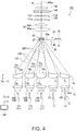
- the collimating optical system 15 includes a plurality of collimating lenses 15a.
- the plurality of collimating lenses 15a are arranged two-dimensionally.
- Each of the plurality of collimating lenses 15a is disposed corresponding to one of the plurality of semiconductor lasers 11. That is, the plurality of collimating lenses 15a are arranged in a matrix (for example, five rows by five columns in Fig. 4 ).
- the collimating lens 15a corresponds to a "condensing lens" in the appended claims.
- each of the plurality of lenses 71 is constituted by a free-form surface lens having a free-form surface.
- Each of the plurality of lenses 71 forms the shape of a spot formed on a region to be illuminated (phosphor layer 42) by a corresponding laser beam LB and makes the illuminance distribution of the spot uniform.
- the plurality of lenses 71 includes a first lens 71a, a second lens 71b, and a third lens 71c.
- the first lens 71a corresponds to the first semiconductor laser 11a
- the second lens 71b corresponds to the second semiconductor laser 11b
- the third lens 71c corresponds to the third semiconductor laser 11c. Therefore, the laser beam LB1 is incident on the first lens 71a, the laser beam LB2 is incident on the second lens 71b, and the laser beam LB3 is incident on the third lens 71c.
- the second condition may be satisfied.
- the first free-form surface 72a and the refractive surface 74a are configured to have a refraction force, and thus it is possible to reduce the refraction force of the refractive surface 74a.
- a cylindrical lens may be used instead of the collimating optical system 15.
- the radiation angle of the laser beam LB has aeolotropy. Therefore, for example, a pair of cylindrical lenses are prepared which have generating lines, respectively, corresponding to a direction having a small radiation angle and a direction having a large radiation angle. Thereby, the laser beam LB having aeolotropy in its radiation angle is satisfactorily collimated, and thus can be caused to be incident on the light shaping optical system 70.
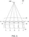
- Fig. 5 is a schematic diagram illustrating a second illumination device of the projector according to the present embodiment.
- a second illumination device 202 of the present embodiment includes a second light source device 710 and a light shaping optical system 20.
- the second light source device 710 has the same configuration as that of the first light source device 10 of the first illumination device 101, and includes a plurality of semiconductor lasers 11.
- the second light source device 710 emits blue light B constituted by a plurality of laser beams LB toward the light shaping optical system 20.
- the second illumination device 202 of the present embodiment it is possible to uniformize the illuminance distribution of the blue light B which is incident on the liquid crystal light modulating device 400B which is a region to be illuminated, with a small number of components, as compared with the lens integrator optical system 740 in which two multi-lens arrays are used.
- the first optical member 171a has a light incident surface 175a, a light emission surface 176a, and a reflection surface 177a.
- Fig. 6 shows only principal rays of light of the laser beams LB which are incident on the respective optical member 171, in order to make the drawing easier to understand.
- the laser beam LB1 reflected from the reflection surface 177a is incident on the light emission surface 176a.
- the light emission surface 176a is constituted by a first lens surface 178a.
- the first lens surface 178a has a first free-form surface 172a specified by a polynomial expression in which x and y are used as variables.
- the first free-form surface 172a is rotationally asymmetrical in shape, and is specified by Expression (1).
- the laser beam LB1 is not refracted when the laser beam is emitted from the light emission surface 276a. Therefore, even in a case where a fluctuation occurs in the refractive index of a glass material due to a temperature change, a variation is not likely to occur in the direction of travel of the laser beam LB1. Thus, since a shift is not likely to occur in a spot forming position on a region to be illuminated, it is possible to efficiently form a spot SP having a rectangular and uniform illuminance distribution on the phosphor layer 42.
- each of the plurality of optical members 271 except the first optical member 271a, the second optical member 271b, and the third optical member 271c also has a free-form surface satisfying the first and third conditions.
- refraction is not also used when light is deflected. Therefore, even in a case where the refractive index of a glass material fluctuates, a variation is not likely to occur in the direction of travel of the laser beam LB. Therefore, according to the light shaping optical system 270 of the present embodiment, the region SA to be illuminated having a rectangular and uniform illuminance distribution can be formed on the phosphor layer 42 with a good degree of accuracy.
- the positions of the respective spots SP are different from each other in the region SA to be illuminated.
- the region SA to be illuminated is the phosphor layer 42
- the intensity of irradiation light per unit area becomes smaller than in a case where the respective spots SP are caused to superpose each other as in the first embodiment.
- the outputs of the respective laser beams LB can also be independently controlled by the control device 160.
- the region SA to be illuminated is set to a light modulating device such as a liquid crystal light modulating device, the illuminance distribution of the region SA to be illuminated which is formed in a light modulating device is adjusted in accordance with an image to be displayed, and thus it is possible to improve the quality of the image.
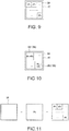
- Fig. 10 is a diagram conceptually illustrating a modification example of the illumination mode of the region to be illuminated.
- the number of spots SP formed on the phosphor layer 42 by laser beams is set to n.
- n spots SP are shown by SP 1 , SP 2 , ⁇ SP n , respectively.
- each of the illumination regions SB is assumed to have a uniform illuminance distribution.
- the region SA to be illuminated which is constituted by the plurality of illumination regions SB has a uniform illuminance distribution, and the same effect as that in the first modification example is exhibited.
- the first light source device 10 is constituted by at least two semiconductor lasers 11 (for example, first semiconductor laser 11a and second semiconductor laser 11b), and that the incident positions of the laser beams LB1 and B2 emitted from the first semiconductor laser 11a and the second semiconductor laser 11b slightly shift from each other due to a mounting error.
- a region (superposed region) partially overlapped in the spots SP formed by the laser beams LB1 and B2 constitutes a region to be illuminated.
- the projector 1 including three liquid crystal light modulating devices 400R, 400G, and 400B has been illustrated as a light modulating device, but the invention can also be applied to a projector that displays a color image using one liquid crystal light modulating device.
- a digital mirror device may be used as the light modulating device.
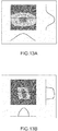
- Example 1 is the simulation results of a lens having a free-form surface satisfying the first condition (the coefficient C j of the x 2h term is different from the coefficient C j of the y 2h term), the second condition (at least one of the first-order term of x and the first-order term of y is included), and the third condition (at least one x p y q term is included). That is, the lens of Example 1 is equivalent to the lens 21 constituting the light shaping optical system 20 of the first embodiment satisfying the first condition to the third condition.
- Table 2 shows respective parameters of Example 2.
- Table 2 Parameter name Example 2 X -0.25 Y -0.75 X 2 -0.01 XY 0.006 Y 2 -0.012 X 4 -0.001 X 3 Y 0.001 Y 4 0.02 Curvature 0.01 Conic constant 0
- Example 2 in Expression (1), the coefficient of the x term is set to -0.25, the coefficient of the y term is set to -0.75, the coefficient of the x 2 term is set to -0.01, the coefficient of the xy term is set to 0.006, the coefficient of the y 2 term is set to -0.012, the coefficient of the x 4 term is set to -0.001, the coefficient of the x 3 y term is set to 0.001, the coefficient of the y 4 term is set to 0.02, a curvature c is set to 0.01, and a conic constant k is set to 0.
- the coefficients of terms which are not written in Table 2 are all 0.
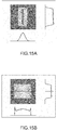
- a rectangular spot having a uniform illuminance distribution is formed in the region to be illuminated.
- the free-form surface lens satisfying the first condition and the second condition is adopted, and thus it has been confirmed that it is possible to form the region to be illuminated in a rectangular shape, and to make the illuminance distribution uniform.
- Example 3 In a case where the free-form surface lens of Example 3 is adopted, it is possible to realize the same illuminance distribution as that in Fig. 12B of Example 1. That is, it has been confirmed that it is possible to form the region to be illuminated in a rectangular shape, and to make the illuminance distribution uniform.
- a diagram illustrating the illuminance distribution relating to Example 3 is the same as that in Example 1, and thus is omitted.
- Table 6 shows respective parameters of Example 6.
- Table 6 Parameter name Example 6 X 2 0.1 Y 2 -0.02 X 4 -0.11 X 6 0 Curvature 0.125 Conic constant 0
Landscapes
- Physics & Mathematics (AREA)
- General Physics & Mathematics (AREA)
- Optics & Photonics (AREA)
- Engineering & Computer Science (AREA)
- General Engineering & Computer Science (AREA)
- Multimedia (AREA)
- Microelectronics & Electronic Packaging (AREA)
- Projection Apparatus (AREA)
- Non-Portable Lighting Devices Or Systems Thereof (AREA)
Claims (12)
- Beleuchtungsvorrichtung (101), umfassend:eine Lichtquellenvorrichtung (10), die ein erstes Licht ausstrahlendes Element (11a) enthält, das zum Ausstrahlen eines ersten Strahlenbündels (LB1) ausgestaltet ist; undein optisches Lichtformungssystem (20), das eine Linse mit einer ersten Linsenfläche (22a) aufweist, auf die das erste Strahlenbündel fällt, unddadurch gekennzeichnet, dassdie erste Linsenfläche eine erste Oberfläche (22a) in freier Form enthält, dargestellt durch Ausdruck (1), in dem x und y als Variable verwendet werden, m und n ganze Zahlen gleich oder größer 0 sind, m1 und n1 ein oberer Grenzwert von m bzw. n sind, k eine konische Konstante ist, c eine Krümmung ist, cj ein Koeffizient von xmyn ist, j= [(m+n)2+m+3n]/2+1, S= [(m1+n1)2+m1+3n1]/2+1 und r= (x2 + y2)1/2, undwenn m=2h und n=2h, wobei h auf eine positive ganze Zahl in Ausdruck (1) eingestellt ist, ein Cj-Koeffizient eines x2-ten-Terms sich von einem Koeffizienten Cj eines y2-ten-Terms unterscheidet

Ausdruck (1) mindestens einen xpyq-Term enthält, falls p und q auf positive ganze Zahlen eingestellt sind. - Beleuchtungsvorrichtung nach Anspruch 1, wobei Ausdruck (1) mindestens einen eines Terms erster Ordnung von x und eines Terms erster Ordnung von y enthält und
der Ausdruck mindestens einen xpyq-Term enthält, falls p und q auf positive ganze Zahlen eingestellt sind. - Beleuchtungsvorrichtung nach Anspruch 1 oder Anspruch 2, wobei ein polynomer Ausdruck von Ausdruck (1) durch einen gerade geordneten Term von x und einen gerade geordneten Term von y dargestellt ist.
- Beleuchtungsvorrichtung nach einem der vorstehenden Ansprüche, wobei das optische Lichtformungssystem weiter eine Reflexionsfläche enthält, die das erste Lichtbündel reflektiert und eine Bewegungsrichtung des ersten Lichtbündels ablenkt, und
Ausdruck (1) mindestens einen xpyq-Term enthält, falls p und q auf positive ganze Zahlen eingestellt sind. - Beleuchtungsvorrichtung nach Anspruch 4, wobei das optische Lichtformungssystem eine Lichteinfallsfläche und eine Lichtausstrahlungsfläche aufweist,
wobei eine der Lichteinfallsfläche und der Lichtausstrahlungsfläche durch die erste Linsenfläche gebildet ist und
ein Hauptlichtstrahl des ersten Lichtbündels auf die andere der Lichteinfallsfläche und der Lichtausstrahlungsfläche in einer zur Oberfläche normalen Richtung fällt. - Beleuchtungsvorrichtung nach einem der vorstehenden Ansprüche, weiter umfassend eine Kondensierungslinse (15), die auf einem Strahlgang des ersten Lichtbündels zwischen dem ersten Lichtausstrahlungselement und der ersten Linsenfläche bereitgestellt ist.
- Beleuchtungsvorrichtung nach einem der vorstehenden Ansprüche, weiter umfassend ein Wellenlängenumwandlungselement (42), auf das das erste Lichtbündel, das durch das optische Lichtformungssystem hindurchgeht, fällt.
- Beleuchtungsvorrichtung nach einem der vorstehenden Ansprüche, wobei die Lichtquellenvorrichtung (10) weiter ein zweites Licht ausstrahlendes Element (11b) enthält, das zum Ausstrahlen eines zweiten Lichtbündels (LB2) ausgebildet ist,
das optische Lichtformungssystem weiter eine zweite Linsenfläche enthält, auf die das zweite Lichtbündel fällt,
die zweite Linsenfläche eine zweite Oberfläche (22b) in freier Form aufweist, die durch Ausdruck (1) dargestellt ist,
der Koeffizient Cj des x2-ten-Terms sich von dem Koeffizienten Cj eines y2-ten-Terms in Bezug auf die zweite Oberfläche in freier Form unterscheidet und
das optische Lichtformungssystem ausgebildet ist, eine Region (SA), die zu beleuchten ist, mit dem ersten Lichtbündel und dem zweiten Lichtbündel in Überlagerung zu beleuchten. - Beleuchtungsvorrichtung nach einem der Ansprüche 1 bis 7, wobei die Lichtquellenvorrichtung weiter ein zweites Licht ausstrahlendes Element (11b) enthält, das zum Ausstrahlen eines zweiten Lichtbündels (LB2) ausgebildet ist,
das optische Lichtformungssystem weiter eine zweite Linsenfläche enthält, auf die das zweite Lichtbündel fällt,
die zweite Linsenfläche eine zweite Oberfläche (22b) in freier Form aufweist, die durch Ausdruck (1) dargestellt ist,
der Koeffizient Cj des x2-ten-Terms sich von dem Koeffizienten Cj des y2-ten-Terms in Bezug auf die zweite Oberfläche in freier Form unterscheidet und
das optische Lichtformungssystem ausgebildet ist, das erste Lichtbündel und das zweite Lichtbündel zu veranlassen, auf Regionen zu fallen, die zu beleuchten sind, die sich voneinander unterscheiden. - Beleuchtungsvorrichtung nach Anspruch 8 oder Anspruch 9, weiter umfassend eine Lichtquellensteuervorrichtung (60), die ausgebildet ist einen Ausgang des ersten Licht ausstrahlenden Elements unabhängig von einem Ausgang des zweiten Licht ausstrahlenden Elements zu steuern.
- Projektor (1), umfassend:die Beleuchtungsvorrichtung nach einem der vorstehenden Ansprüche;eine Lichtmodulationsvorrichtung (400R, 400G, 400B), die ausgebildet ist, Beleuchtungslicht, das von der Beleuchtungsvorrichtung ausgestrahlt wird, gemäß Bildinformationen zu modulieren und Bildlicht zu erzeugen; undein optisches Projektionssystem (600), das ausgebildet ist, das Bildlicht zu projizieren,wobei eine Bilderzeugungsregion der Lichtmodulationsvorrichtung der zu beleuchtenden Region äquivalent ist.
- Projektor nach Anspruch 11,
wobei die Lichtquellenvorrichtung weiter ein drittes Licht ausstrahlendes Element (11c) enthält, das ausgebildet ist, ein drittes Lichtbündel (LB3) auszustrahlen,
das optische Lichtformungssystem weiter eine dritte Linsenfläche enthält, auf die das dritte Lichtbündel einfällt,
die dritte Linsenfläche eine dritte Oberfläche (22c) in freier Form aufweist, die durch Ausdruck (1) dargestellt ist,
der Koeffizient Cj des x2-ten-Terms sich von dem Koeffizienten Cj des y2-ten-Terms in Bezug auf die dritte Oberfläche in freier Form unterscheidet,
das optische Lichtformungssystem ausgebildet ist eine gesamte zu beleuchtende Region mit dem dritten Lichtbündel zu beleuchten,
die Lichtquellensteuervorrichtung (60) ausgebildet ist, einen Ausgang des dritten Licht ausstrahlenden Elements unabhängig von mindestens einem Ausgang des ersten Licht ausstrahlenden Elements und einem Ausgang des zweiten Licht ausstrahlenden Elements zu steuern und eine Bilderzeugungsregion der Lichtmodulationsvorrichtung der zu beleuchtenden Region äquivalent ist.
Applications Claiming Priority (2)
| Application Number | Priority Date | Filing Date | Title |
|---|---|---|---|
| JP2017009613 | 2017-01-23 | ||
| JP2017150294A JP6950339B2 (ja) | 2017-01-23 | 2017-08-02 | 照明装置及びプロジェクター |
Publications (2)
| Publication Number | Publication Date |
|---|---|
| EP3351997A1 EP3351997A1 (de) | 2018-07-25 |
| EP3351997B1 true EP3351997B1 (de) | 2020-07-29 |
Family
ID=61017840
Family Applications (1)
| Application Number | Title | Priority Date | Filing Date |
|---|---|---|---|
| EP18152719.3A Active EP3351997B1 (de) | 2017-01-23 | 2018-01-22 | Beleuchtungsvorrichtung und projektor |
Country Status (3)
| Country | Link |
|---|---|
| US (1) | US10268113B2 (de) |
| EP (1) | EP3351997B1 (de) |
| CN (1) | CN108345162B (de) |
Families Citing this family (6)
| Publication number | Priority date | Publication date | Assignee | Title |
|---|---|---|---|---|
| CN108572497B (zh) * | 2017-03-14 | 2019-12-17 | 深圳光峰科技股份有限公司 | 光源装置及投影系统 |
| JP7087828B2 (ja) * | 2018-08-27 | 2022-06-21 | セイコーエプソン株式会社 | 光学素子、光射出装置および画像表示システム |
| JP7363411B2 (ja) * | 2019-11-25 | 2023-10-18 | セイコーエプソン株式会社 | 光源装置およびプロジェクター |
| JP2022037336A (ja) * | 2020-08-25 | 2022-03-09 | セイコーエプソン株式会社 | 光源装置、画像表示装置、およびプロジェクター |
| CA3130380C (en) * | 2020-09-10 | 2026-04-21 | Saco Technologies Inc. | Light shaping assembly having light sources mounted on a pcb via supporting pins bent for orienting light toward a projector lens |
| EP4260111B1 (de) * | 2020-12-14 | 2025-06-11 | Jabil Optics Germany GmbH | Umgebungssicht-abbildungssystem |
Citations (1)
| Publication number | Priority date | Publication date | Assignee | Title |
|---|---|---|---|---|
| JP2009217060A (ja) * | 2008-03-11 | 2009-09-24 | Nikon Corp | プロジェクタ装置 |
Family Cites Families (16)
| Publication number | Priority date | Publication date | Assignee | Title |
|---|---|---|---|---|
| JP2003121777A (ja) | 2001-10-18 | 2003-04-23 | Sony Corp | レンズアレイを用いた照明装置及び画像表示装置 |
| JP4661149B2 (ja) | 2003-12-22 | 2011-03-30 | セイコーエプソン株式会社 | 照明装置及びプロジェクタ |
| JP2007171319A (ja) * | 2005-12-20 | 2007-07-05 | Samsung Electronics Co Ltd | 照明光学系、それを用いた照明ユニットおよび画像投影装置 |
| JP2009294639A (ja) * | 2008-05-02 | 2009-12-17 | Seiko Epson Corp | 照明装置、プロジェクタ、照明方法 |
| JP5436097B2 (ja) * | 2009-08-25 | 2014-03-05 | 三菱電機株式会社 | 集光光学系及び投写型画像表示装置 |
| JP2011107358A (ja) | 2009-11-17 | 2011-06-02 | Nikon Corp | 照明光学系及びプロジェクタ |
| JP5527594B2 (ja) | 2010-03-24 | 2014-06-18 | カシオ計算機株式会社 | 光源ユニット及びプロジェクタ |
| JP5445379B2 (ja) * | 2010-07-30 | 2014-03-19 | セイコーエプソン株式会社 | プロジェクター |
| JP5699568B2 (ja) * | 2010-11-29 | 2015-04-15 | セイコーエプソン株式会社 | 光源装置、プロジェクター |
| JP5685996B2 (ja) * | 2011-03-08 | 2015-03-18 | セイコーエプソン株式会社 | 照明装置およびプロジェクター |
| JP5967976B2 (ja) | 2012-02-29 | 2016-08-10 | 日東光学株式会社 | 照明光学系および照明装置 |
| CN103365051B (zh) * | 2012-04-01 | 2016-08-03 | 欧司朗股份有限公司 | 照明装置及投影仪 |
| US9575403B2 (en) * | 2012-08-21 | 2017-02-21 | Nec Display Solutions, Ltd. | Illumination optical system, projector, and projector system |
| JP2014138148A (ja) | 2013-01-18 | 2014-07-28 | Hitachi Media Electoronics Co Ltd | 半導体レーザ、半導体レーザアレイおよび画像表示装置 |
| CN104937487B (zh) * | 2013-01-23 | 2017-04-19 | 三菱电机株式会社 | 投影型显示装置 |
| CN105221974B (zh) | 2014-06-13 | 2017-05-31 | 清华大学 | 基于xy多项式的led自由曲面照明系统的设计方法 |
-
2018
- 2018-01-16 US US15/872,868 patent/US10268113B2/en active Active
- 2018-01-18 CN CN201810048309.6A patent/CN108345162B/zh active Active
- 2018-01-22 EP EP18152719.3A patent/EP3351997B1/de active Active
Patent Citations (1)
| Publication number | Priority date | Publication date | Assignee | Title |
|---|---|---|---|---|
| JP2009217060A (ja) * | 2008-03-11 | 2009-09-24 | Nikon Corp | プロジェクタ装置 |
Also Published As
| Publication number | Publication date |
|---|---|
| CN108345162B (zh) | 2020-10-13 |
| CN108345162A (zh) | 2018-07-31 |
| EP3351997A1 (de) | 2018-07-25 |
| US20180210328A1 (en) | 2018-07-26 |
| US10268113B2 (en) | 2019-04-23 |
Similar Documents
| Publication | Publication Date | Title |
|---|---|---|
| EP3351997B1 (de) | Beleuchtungsvorrichtung und projektor | |
| CN203232239U (zh) | 光源装置及投影机 | |
| US9310033B2 (en) | Light source device and projection-type display apparatus | |
| US8840251B2 (en) | Light collecting optical system and projection-type image display apparatus | |
| JP5884743B2 (ja) | 照明装置および表示装置 | |
| US8596795B2 (en) | Projector | |
| CN103959126B (zh) | 投影光学系统和投影型图像显示装置 | |
| JP7031567B2 (ja) | 光源光学系、光源装置及び画像投射装置 | |
| US9261765B2 (en) | Light converging optical system and projection-type image display apparatus | |
| US7946711B2 (en) | Illumination device and projection display device | |
| US10203590B2 (en) | Illuminator and projector | |
| CN104736931A (zh) | 光源单元、光源装置以及图像显示装置 | |
| EP2017669A2 (de) | Beleuchtungsvorrichtung, Projektionsvideo-Anzeigevorrichtung und Fliegenaugenlinse | |
| US11709416B2 (en) | Light source device, image display device, and projector | |
| JP6239157B2 (ja) | レーザ光源装置および映像表示装置 | |
| US11630382B2 (en) | Optical element, light source device, image display device, and projector | |
| JP2017053876A (ja) | 投写型画像表示装置 | |
| KR20110135568A (ko) | 조명광학유닛 및 이를 가지는 디스플레이장치 | |
| JP6950339B2 (ja) | 照明装置及びプロジェクター | |
| JP2018120025A (ja) | 照明装置及びプロジェクター | |
| US20240319575A1 (en) | Projector | |
| US10838292B2 (en) | Light source apparatus, illuminator, and projector | |
| JP2017147195A (ja) | 光源装置及びプロジェクター | |
| JP2014062985A (ja) | 投写型表示装置 | |
| JP6194967B2 (ja) | 照明装置および表示装置 |
Legal Events
| Date | Code | Title | Description |
|---|---|---|---|
| PUAI | Public reference made under article 153(3) epc to a published international application that has entered the european phase |
Free format text: ORIGINAL CODE: 0009012 |
|
| STAA | Information on the status of an ep patent application or granted ep patent |
Free format text: STATUS: THE APPLICATION HAS BEEN PUBLISHED |
|
| AK | Designated contracting states |
Kind code of ref document: A1 Designated state(s): AL AT BE BG CH CY CZ DE DK EE ES FI FR GB GR HR HU IE IS IT LI LT LU LV MC MK MT NL NO PL PT RO RS SE SI SK SM TR |
|
| AX | Request for extension of the european patent |
Extension state: BA ME |
|
| STAA | Information on the status of an ep patent application or granted ep patent |
Free format text: STATUS: REQUEST FOR EXAMINATION WAS MADE |
|
| 17P | Request for examination filed |
Effective date: 20190125 |
|
| RBV | Designated contracting states (corrected) |
Designated state(s): AL AT BE BG CH CY CZ DE DK EE ES FI FR GB GR HR HU IE IS IT LI LT LU LV MC MK MT NL NO PL PT RO RS SE SI SK SM TR |
|
| STAA | Information on the status of an ep patent application or granted ep patent |
Free format text: STATUS: EXAMINATION IS IN PROGRESS |
|
| 17Q | First examination report despatched |
Effective date: 20190412 |
|
| GRAP | Despatch of communication of intention to grant a patent |
Free format text: ORIGINAL CODE: EPIDOSNIGR1 |
|
| STAA | Information on the status of an ep patent application or granted ep patent |
Free format text: STATUS: GRANT OF PATENT IS INTENDED |
|
| INTG | Intention to grant announced |
Effective date: 20200224 |
|
| GRAS | Grant fee paid |
Free format text: ORIGINAL CODE: EPIDOSNIGR3 |
|
| GRAA | (expected) grant |
Free format text: ORIGINAL CODE: 0009210 |
|
| STAA | Information on the status of an ep patent application or granted ep patent |
Free format text: STATUS: THE PATENT HAS BEEN GRANTED |
|
| AK | Designated contracting states |
Kind code of ref document: B1 Designated state(s): AL AT BE BG CH CY CZ DE DK EE ES FI FR GB GR HR HU IE IS IT LI LT LU LV MC MK MT NL NO PL PT RO RS SE SI SK SM TR |
|
| REG | Reference to a national code |
Ref country code: CH Ref legal event code: EP |
|
| REG | Reference to a national code |
Ref country code: AT Ref legal event code: REF Ref document number: 1296473 Country of ref document: AT Kind code of ref document: T Effective date: 20200815 |
|
| REG | Reference to a national code |
Ref country code: IE Ref legal event code: FG4D |
|
| REG | Reference to a national code |
Ref country code: DE Ref legal event code: R096 Ref document number: 602018006306 Country of ref document: DE |
|
| REG | Reference to a national code |
Ref country code: LT Ref legal event code: MG4D |
|
| REG | Reference to a national code |
Ref country code: NL Ref legal event code: MP Effective date: 20200729 |
|
| REG | Reference to a national code |
Ref country code: AT Ref legal event code: MK05 Ref document number: 1296473 Country of ref document: AT Kind code of ref document: T Effective date: 20200729 |
|
| PG25 | Lapsed in a contracting state [announced via postgrant information from national office to epo] |
Ref country code: AT Free format text: LAPSE BECAUSE OF FAILURE TO SUBMIT A TRANSLATION OF THE DESCRIPTION OR TO PAY THE FEE WITHIN THE PRESCRIBED TIME-LIMIT Effective date: 20200729 Ref country code: PT Free format text: LAPSE BECAUSE OF FAILURE TO SUBMIT A TRANSLATION OF THE DESCRIPTION OR TO PAY THE FEE WITHIN THE PRESCRIBED TIME-LIMIT Effective date: 20201130 Ref country code: GR Free format text: LAPSE BECAUSE OF FAILURE TO SUBMIT A TRANSLATION OF THE DESCRIPTION OR TO PAY THE FEE WITHIN THE PRESCRIBED TIME-LIMIT Effective date: 20201030 Ref country code: FI Free format text: LAPSE BECAUSE OF FAILURE TO SUBMIT A TRANSLATION OF THE DESCRIPTION OR TO PAY THE FEE WITHIN THE PRESCRIBED TIME-LIMIT Effective date: 20200729 Ref country code: HR Free format text: LAPSE BECAUSE OF FAILURE TO SUBMIT A TRANSLATION OF THE DESCRIPTION OR TO PAY THE FEE WITHIN THE PRESCRIBED TIME-LIMIT Effective date: 20200729 Ref country code: LT Free format text: LAPSE BECAUSE OF FAILURE TO SUBMIT A TRANSLATION OF THE DESCRIPTION OR TO PAY THE FEE WITHIN THE PRESCRIBED TIME-LIMIT Effective date: 20200729 Ref country code: BG Free format text: LAPSE BECAUSE OF FAILURE TO SUBMIT A TRANSLATION OF THE DESCRIPTION OR TO PAY THE FEE WITHIN THE PRESCRIBED TIME-LIMIT Effective date: 20201029 Ref country code: SE Free format text: LAPSE BECAUSE OF FAILURE TO SUBMIT A TRANSLATION OF THE DESCRIPTION OR TO PAY THE FEE WITHIN THE PRESCRIBED TIME-LIMIT Effective date: 20200729 Ref country code: ES Free format text: LAPSE BECAUSE OF FAILURE TO SUBMIT A TRANSLATION OF THE DESCRIPTION OR TO PAY THE FEE WITHIN THE PRESCRIBED TIME-LIMIT Effective date: 20200729 Ref country code: NO Free format text: LAPSE BECAUSE OF FAILURE TO SUBMIT A TRANSLATION OF THE DESCRIPTION OR TO PAY THE FEE WITHIN THE PRESCRIBED TIME-LIMIT Effective date: 20201029 |
|
| PG25 | Lapsed in a contracting state [announced via postgrant information from national office to epo] |
Ref country code: IS Free format text: LAPSE BECAUSE OF FAILURE TO SUBMIT A TRANSLATION OF THE DESCRIPTION OR TO PAY THE FEE WITHIN THE PRESCRIBED TIME-LIMIT Effective date: 20201129 Ref country code: LV Free format text: LAPSE BECAUSE OF FAILURE TO SUBMIT A TRANSLATION OF THE DESCRIPTION OR TO PAY THE FEE WITHIN THE PRESCRIBED TIME-LIMIT Effective date: 20200729 Ref country code: PL Free format text: LAPSE BECAUSE OF FAILURE TO SUBMIT A TRANSLATION OF THE DESCRIPTION OR TO PAY THE FEE WITHIN THE PRESCRIBED TIME-LIMIT Effective date: 20200729 Ref country code: RS Free format text: LAPSE BECAUSE OF FAILURE TO SUBMIT A TRANSLATION OF THE DESCRIPTION OR TO PAY THE FEE WITHIN THE PRESCRIBED TIME-LIMIT Effective date: 20200729 |
|
| PG25 | Lapsed in a contracting state [announced via postgrant information from national office to epo] |
Ref country code: NL Free format text: LAPSE BECAUSE OF FAILURE TO SUBMIT A TRANSLATION OF THE DESCRIPTION OR TO PAY THE FEE WITHIN THE PRESCRIBED TIME-LIMIT Effective date: 20200729 |
|
| PG25 | Lapsed in a contracting state [announced via postgrant information from national office to epo] |
Ref country code: IT Free format text: LAPSE BECAUSE OF FAILURE TO SUBMIT A TRANSLATION OF THE DESCRIPTION OR TO PAY THE FEE WITHIN THE PRESCRIBED TIME-LIMIT Effective date: 20200729 Ref country code: SM Free format text: LAPSE BECAUSE OF FAILURE TO SUBMIT A TRANSLATION OF THE DESCRIPTION OR TO PAY THE FEE WITHIN THE PRESCRIBED TIME-LIMIT Effective date: 20200729 Ref country code: DK Free format text: LAPSE BECAUSE OF FAILURE TO SUBMIT A TRANSLATION OF THE DESCRIPTION OR TO PAY THE FEE WITHIN THE PRESCRIBED TIME-LIMIT Effective date: 20200729 Ref country code: CZ Free format text: LAPSE BECAUSE OF FAILURE TO SUBMIT A TRANSLATION OF THE DESCRIPTION OR TO PAY THE FEE WITHIN THE PRESCRIBED TIME-LIMIT Effective date: 20200729 Ref country code: RO Free format text: LAPSE BECAUSE OF FAILURE TO SUBMIT A TRANSLATION OF THE DESCRIPTION OR TO PAY THE FEE WITHIN THE PRESCRIBED TIME-LIMIT Effective date: 20200729 Ref country code: EE Free format text: LAPSE BECAUSE OF FAILURE TO SUBMIT A TRANSLATION OF THE DESCRIPTION OR TO PAY THE FEE WITHIN THE PRESCRIBED TIME-LIMIT Effective date: 20200729 |
|
| REG | Reference to a national code |
Ref country code: DE Ref legal event code: R097 Ref document number: 602018006306 Country of ref document: DE |
|
| PG25 | Lapsed in a contracting state [announced via postgrant information from national office to epo] |
Ref country code: AL Free format text: LAPSE BECAUSE OF FAILURE TO SUBMIT A TRANSLATION OF THE DESCRIPTION OR TO PAY THE FEE WITHIN THE PRESCRIBED TIME-LIMIT Effective date: 20200729 |
|
| PLBE | No opposition filed within time limit |
Free format text: ORIGINAL CODE: 0009261 |
|
| STAA | Information on the status of an ep patent application or granted ep patent |
Free format text: STATUS: NO OPPOSITION FILED WITHIN TIME LIMIT |
|
| PG25 | Lapsed in a contracting state [announced via postgrant information from national office to epo] |
Ref country code: SK Free format text: LAPSE BECAUSE OF FAILURE TO SUBMIT A TRANSLATION OF THE DESCRIPTION OR TO PAY THE FEE WITHIN THE PRESCRIBED TIME-LIMIT Effective date: 20200729 |
|
| 26N | No opposition filed |
Effective date: 20210430 |
|
| PG25 | Lapsed in a contracting state [announced via postgrant information from national office to epo] |
Ref country code: MC Free format text: LAPSE BECAUSE OF FAILURE TO SUBMIT A TRANSLATION OF THE DESCRIPTION OR TO PAY THE FEE WITHIN THE PRESCRIBED TIME-LIMIT Effective date: 20200729 Ref country code: SI Free format text: LAPSE BECAUSE OF FAILURE TO SUBMIT A TRANSLATION OF THE DESCRIPTION OR TO PAY THE FEE WITHIN THE PRESCRIBED TIME-LIMIT Effective date: 20200729 |
|
| REG | Reference to a national code |
Ref country code: CH Ref legal event code: PL |
|
| PG25 | Lapsed in a contracting state [announced via postgrant information from national office to epo] |
Ref country code: LU Free format text: LAPSE BECAUSE OF NON-PAYMENT OF DUE FEES Effective date: 20210122 |
|
| REG | Reference to a national code |
Ref country code: BE Ref legal event code: MM Effective date: 20210131 |
|
| PG25 | Lapsed in a contracting state [announced via postgrant information from national office to epo] |
Ref country code: CH Free format text: LAPSE BECAUSE OF NON-PAYMENT OF DUE FEES Effective date: 20210131 Ref country code: LI Free format text: LAPSE BECAUSE OF NON-PAYMENT OF DUE FEES Effective date: 20210131 |
|
| PG25 | Lapsed in a contracting state [announced via postgrant information from national office to epo] |
Ref country code: IE Free format text: LAPSE BECAUSE OF NON-PAYMENT OF DUE FEES Effective date: 20210122 |
|
| PG25 | Lapsed in a contracting state [announced via postgrant information from national office to epo] |
Ref country code: BE Free format text: LAPSE BECAUSE OF NON-PAYMENT OF DUE FEES Effective date: 20210131 |
|
| PG25 | Lapsed in a contracting state [announced via postgrant information from national office to epo] |
Ref country code: CY Free format text: LAPSE BECAUSE OF FAILURE TO SUBMIT A TRANSLATION OF THE DESCRIPTION OR TO PAY THE FEE WITHIN THE PRESCRIBED TIME-LIMIT Effective date: 20200729 |
|
| PG25 | Lapsed in a contracting state [announced via postgrant information from national office to epo] |
Ref country code: HU Free format text: LAPSE BECAUSE OF FAILURE TO SUBMIT A TRANSLATION OF THE DESCRIPTION OR TO PAY THE FEE WITHIN THE PRESCRIBED TIME-LIMIT; INVALID AB INITIO Effective date: 20180122 |
|
| PG25 | Lapsed in a contracting state [announced via postgrant information from national office to epo] |
Ref country code: MK Free format text: LAPSE BECAUSE OF FAILURE TO SUBMIT A TRANSLATION OF THE DESCRIPTION OR TO PAY THE FEE WITHIN THE PRESCRIBED TIME-LIMIT Effective date: 20200729 |
|
| PG25 | Lapsed in a contracting state [announced via postgrant information from national office to epo] |
Ref country code: MT Free format text: LAPSE BECAUSE OF FAILURE TO SUBMIT A TRANSLATION OF THE DESCRIPTION OR TO PAY THE FEE WITHIN THE PRESCRIBED TIME-LIMIT Effective date: 20200729 |
|
| PG25 | Lapsed in a contracting state [announced via postgrant information from national office to epo] |
Ref country code: TR Free format text: LAPSE BECAUSE OF FAILURE TO SUBMIT A TRANSLATION OF THE DESCRIPTION OR TO PAY THE FEE WITHIN THE PRESCRIBED TIME-LIMIT Effective date: 20200729 |
|
| PGFP | Annual fee paid to national office [announced via postgrant information from national office to epo] |
Ref country code: GB Payment date: 20251204 Year of fee payment: 9 |
|
| PGFP | Annual fee paid to national office [announced via postgrant information from national office to epo] |
Ref country code: FR Payment date: 20251128 Year of fee payment: 9 |
|
| PGFP | Annual fee paid to national office [announced via postgrant information from national office to epo] |
Ref country code: DE Payment date: 20251203 Year of fee payment: 9 |