EP3350836B1 - Verfahren zur herstellung eines strahlungsdetektors sowie strahlungsdetektor - Google Patents
Verfahren zur herstellung eines strahlungsdetektors sowie strahlungsdetektor Download PDFInfo
- Publication number
- EP3350836B1 EP3350836B1 EP16767258.3A EP16767258A EP3350836B1 EP 3350836 B1 EP3350836 B1 EP 3350836B1 EP 16767258 A EP16767258 A EP 16767258A EP 3350836 B1 EP3350836 B1 EP 3350836B1
- Authority
- EP
- European Patent Office
- Prior art keywords
- layer
- detector
- inorganic
- organic halide
- radiation
- Prior art date
- Legal status (The legal status is an assumption and is not a legal conclusion. Google has not performed a legal analysis and makes no representation as to the accuracy of the status listed.)
- Active
Links
- 230000005855 radiation Effects 0.000 title claims description 49
- 238000004519 manufacturing process Methods 0.000 title claims description 7
- 239000000463 material Substances 0.000 claims description 80
- 150000004820 halides Chemical class 0.000 claims description 35
- 238000010899 nucleation Methods 0.000 claims description 28
- 238000000034 method Methods 0.000 claims description 22
- 239000000758 substrate Substances 0.000 claims description 19
- 230000000903 blocking effect Effects 0.000 claims description 16
- -1 methyl ammonium metal halide Chemical class 0.000 claims description 9
- 229910001507 metal halide Inorganic materials 0.000 claims description 8
- BAVYZALUXZFZLV-UHFFFAOYSA-N Methylamine Chemical compound NC BAVYZALUXZFZLV-UHFFFAOYSA-N 0.000 claims description 7
- 238000000151 deposition Methods 0.000 claims description 7
- 239000002184 metal Substances 0.000 claims description 7
- 229910052751 metal Inorganic materials 0.000 claims description 7
- 238000007788 roughening Methods 0.000 claims description 7
- XMBWDFGMSWQBCA-UHFFFAOYSA-N hydrogen iodide Chemical compound I XMBWDFGMSWQBCA-UHFFFAOYSA-N 0.000 claims description 6
- 230000005865 ionizing radiation Effects 0.000 claims description 6
- 239000002245 particle Substances 0.000 claims description 6
- QTBSBXVTEAMEQO-UHFFFAOYSA-M Acetate Chemical compound CC([O-])=O QTBSBXVTEAMEQO-UHFFFAOYSA-M 0.000 claims description 5
- 229910000043 hydrogen iodide Inorganic materials 0.000 claims description 4
- CPELXLSAUQHCOX-UHFFFAOYSA-M Bromide Chemical compound [Br-] CPELXLSAUQHCOX-UHFFFAOYSA-M 0.000 claims description 3
- 230000008021 deposition Effects 0.000 claims description 3
- 239000000203 mixture Substances 0.000 claims description 3
- OAICVXFJPJFONN-UHFFFAOYSA-N Phosphorus Chemical compound [P] OAICVXFJPJFONN-UHFFFAOYSA-N 0.000 claims description 2
- 150000005309 metal halides Chemical class 0.000 claims description 2
- 239000002096 quantum dot Substances 0.000 claims description 2
- 238000007650 screen-printing Methods 0.000 claims description 2
- 239000010410 layer Substances 0.000 description 106
- 238000001514 detection method Methods 0.000 description 17
- 238000006243 chemical reaction Methods 0.000 description 14
- 239000013078 crystal Substances 0.000 description 9
- 239000000243 solution Substances 0.000 description 9
- 238000010521 absorption reaction Methods 0.000 description 8
- 238000010586 diagram Methods 0.000 description 8
- 230000008901 benefit Effects 0.000 description 7
- 238000002591 computed tomography Methods 0.000 description 6
- 125000005843 halogen group Chemical group 0.000 description 6
- 238000012636 positron electron tomography Methods 0.000 description 6
- 230000004048 modification Effects 0.000 description 5
- 238000012986 modification Methods 0.000 description 5
- 238000013459 approach Methods 0.000 description 4
- QWUZMTJBRUASOW-UHFFFAOYSA-N cadmium tellanylidenezinc Chemical compound [Zn].[Cd].[Te] QWUZMTJBRUASOW-UHFFFAOYSA-N 0.000 description 4
- 239000002800 charge carrier Substances 0.000 description 4
- 230000005684 electric field Effects 0.000 description 4
- 239000011521 glass Substances 0.000 description 4
- 125000000623 heterocyclic group Chemical group 0.000 description 4
- 125000001183 hydrocarbyl group Chemical group 0.000 description 4
- 230000008569 process Effects 0.000 description 4
- 230000001419 dependent effect Effects 0.000 description 3
- 238000003384 imaging method Methods 0.000 description 3
- 238000009607 mammography Methods 0.000 description 3
- 150000002739 metals Chemical class 0.000 description 3
- 239000011669 selenium Substances 0.000 description 3
- 239000004065 semiconductor Substances 0.000 description 3
- 238000004528 spin coating Methods 0.000 description 3
- VYPSYNLAJGMNEJ-UHFFFAOYSA-N Silicium dioxide Chemical compound O=[Si]=O VYPSYNLAJGMNEJ-UHFFFAOYSA-N 0.000 description 2
- 239000012190 activator Substances 0.000 description 2
- 230000015572 biosynthetic process Effects 0.000 description 2
- 150000001875 compounds Chemical class 0.000 description 2
- 238000002347 injection Methods 0.000 description 2
- 239000007924 injection Substances 0.000 description 2
- 150000002500 ions Chemical class 0.000 description 2
- HTUMBQDCCIXGCV-UHFFFAOYSA-N lead oxide Chemical compound [O-2].[Pb+2] HTUMBQDCCIXGCV-UHFFFAOYSA-N 0.000 description 2
- 238000012831 peritoneal equilibrium test Methods 0.000 description 2
- 238000012877 positron emission topography Methods 0.000 description 2
- 230000004044 response Effects 0.000 description 2
- 230000035945 sensitivity Effects 0.000 description 2
- 238000002603 single-photon emission computed tomography Methods 0.000 description 2
- 238000001228 spectrum Methods 0.000 description 2
- 230000002123 temporal effect Effects 0.000 description 2
- 238000012879 PET imaging Methods 0.000 description 1
- BUGBHKTXTAQXES-UHFFFAOYSA-N Selenium Chemical compound [Se] BUGBHKTXTAQXES-UHFFFAOYSA-N 0.000 description 1
- XUIMIQQOPSSXEZ-UHFFFAOYSA-N Silicon Chemical compound [Si] XUIMIQQOPSSXEZ-UHFFFAOYSA-N 0.000 description 1
- 230000004913 activation Effects 0.000 description 1
- 125000000217 alkyl group Chemical group 0.000 description 1
- 125000004429 atom Chemical group 0.000 description 1
- 230000009286 beneficial effect Effects 0.000 description 1
- 230000008033 biological extinction Effects 0.000 description 1
- 230000008859 change Effects 0.000 description 1
- 238000005229 chemical vapour deposition Methods 0.000 description 1
- 229910052681 coesite Inorganic materials 0.000 description 1
- 239000004020 conductor Substances 0.000 description 1
- 229910052802 copper Inorganic materials 0.000 description 1
- 229910052906 cristobalite Inorganic materials 0.000 description 1
- 125000004122 cyclic group Chemical group 0.000 description 1
- 230000001066 destructive effect Effects 0.000 description 1
- 238000009826 distribution Methods 0.000 description 1
- 230000000694 effects Effects 0.000 description 1
- 239000007772 electrode material Substances 0.000 description 1
- 238000010894 electron beam technology Methods 0.000 description 1
- 230000007613 environmental effect Effects 0.000 description 1
- 125000004435 hydrogen atom Chemical group [H]* 0.000 description 1
- 229910052500 inorganic mineral Inorganic materials 0.000 description 1
- 238000007689 inspection Methods 0.000 description 1
- 229910052742 iron Inorganic materials 0.000 description 1
- 230000031700 light absorption Effects 0.000 description 1
- 229910052748 manganese Inorganic materials 0.000 description 1
- 239000011707 mineral Substances 0.000 description 1
- 230000007935 neutral effect Effects 0.000 description 1
- 238000009206 nuclear medicine Methods 0.000 description 1
- 125000000962 organic group Chemical group 0.000 description 1
- 239000012044 organic layer Substances 0.000 description 1
- 229910052763 palladium Inorganic materials 0.000 description 1
- 238000005240 physical vapour deposition Methods 0.000 description 1
- 229920000642 polymer Polymers 0.000 description 1
- 230000009467 reduction Effects 0.000 description 1
- 229910052711 selenium Inorganic materials 0.000 description 1
- 229910052710 silicon Inorganic materials 0.000 description 1
- 239000010703 silicon Substances 0.000 description 1
- 239000000377 silicon dioxide Substances 0.000 description 1
- 230000003595 spectral effect Effects 0.000 description 1
- 229910052682 stishovite Inorganic materials 0.000 description 1
- 239000000126 substance Substances 0.000 description 1
- 229910052905 tridymite Inorganic materials 0.000 description 1
- 238000007738 vacuum evaporation Methods 0.000 description 1
- XLYOFNOQVPJJNP-UHFFFAOYSA-N water Substances O XLYOFNOQVPJJNP-UHFFFAOYSA-N 0.000 description 1
Images
Classifications
-
- H—ELECTRICITY
- H10—SEMICONDUCTOR DEVICES; ELECTRIC SOLID-STATE DEVICES NOT OTHERWISE PROVIDED FOR
- H10K—ORGANIC ELECTRIC SOLID-STATE DEVICES
- H10K39/00—Integrated devices, or assemblies of multiple devices, comprising at least one organic radiation-sensitive element covered by group H10K30/00
- H10K39/30—Devices controlled by radiation
- H10K39/36—Devices specially adapted for detecting X-ray radiation
-
- G—PHYSICS
- G01—MEASURING; TESTING
- G01T—MEASUREMENT OF NUCLEAR OR X-RADIATION
- G01T1/00—Measuring X-radiation, gamma radiation, corpuscular radiation, or cosmic radiation
- G01T1/16—Measuring radiation intensity
- G01T1/20—Measuring radiation intensity with scintillation detectors
- G01T1/2018—Scintillation-photodiode combinations
-
- G—PHYSICS
- G01—MEASURING; TESTING
- G01T—MEASUREMENT OF NUCLEAR OR X-RADIATION
- G01T1/00—Measuring X-radiation, gamma radiation, corpuscular radiation, or cosmic radiation
- G01T1/16—Measuring radiation intensity
- G01T1/20—Measuring radiation intensity with scintillation detectors
- G01T1/202—Measuring radiation intensity with scintillation detectors the detector being a crystal
- G01T1/2023—Selection of materials
-
- G—PHYSICS
- G01—MEASURING; TESTING
- G01T—MEASUREMENT OF NUCLEAR OR X-RADIATION
- G01T1/00—Measuring X-radiation, gamma radiation, corpuscular radiation, or cosmic radiation
- G01T1/16—Measuring radiation intensity
- G01T1/24—Measuring radiation intensity with semiconductor detectors
-
- G—PHYSICS
- G01—MEASURING; TESTING
- G01T—MEASUREMENT OF NUCLEAR OR X-RADIATION
- G01T1/00—Measuring X-radiation, gamma radiation, corpuscular radiation, or cosmic radiation
- G01T1/16—Measuring radiation intensity
- G01T1/24—Measuring radiation intensity with semiconductor detectors
- G01T1/241—Electrode arrangements, e.g. continuous or parallel strips or the like
-
- H—ELECTRICITY
- H10—SEMICONDUCTOR DEVICES; ELECTRIC SOLID-STATE DEVICES NOT OTHERWISE PROVIDED FOR
- H10K—ORGANIC ELECTRIC SOLID-STATE DEVICES
- H10K30/00—Organic devices sensitive to infrared radiation, light, electromagnetic radiation of shorter wavelength or corpuscular radiation
- H10K30/30—Organic devices sensitive to infrared radiation, light, electromagnetic radiation of shorter wavelength or corpuscular radiation comprising bulk heterojunctions, e.g. interpenetrating networks of donor and acceptor material domains
- H10K30/353—Organic devices sensitive to infrared radiation, light, electromagnetic radiation of shorter wavelength or corpuscular radiation comprising bulk heterojunctions, e.g. interpenetrating networks of donor and acceptor material domains comprising blocking layers, e.g. exciton blocking layers
-
- H—ELECTRICITY
- H10—SEMICONDUCTOR DEVICES; ELECTRIC SOLID-STATE DEVICES NOT OTHERWISE PROVIDED FOR
- H10K—ORGANIC ELECTRIC SOLID-STATE DEVICES
- H10K30/00—Organic devices sensitive to infrared radiation, light, electromagnetic radiation of shorter wavelength or corpuscular radiation
- H10K30/80—Constructional details
- H10K30/81—Electrodes
-
- H—ELECTRICITY
- H10—SEMICONDUCTOR DEVICES; ELECTRIC SOLID-STATE DEVICES NOT OTHERWISE PROVIDED FOR
- H10K—ORGANIC ELECTRIC SOLID-STATE DEVICES
- H10K71/00—Manufacture or treatment specially adapted for the organic devices covered by this subclass
- H10K71/10—Deposition of organic active material
- H10K71/12—Deposition of organic active material using liquid deposition, e.g. spin coating
-
- H—ELECTRICITY
- H10—SEMICONDUCTOR DEVICES; ELECTRIC SOLID-STATE DEVICES NOT OTHERWISE PROVIDED FOR
- H10K—ORGANIC ELECTRIC SOLID-STATE DEVICES
- H10K85/00—Organic materials used in the body or electrodes of devices covered by this subclass
- H10K85/50—Organic perovskites; Hybrid organic-inorganic perovskites [HOIP], e.g. CH3NH3PbI3
-
- H—ELECTRICITY
- H10—SEMICONDUCTOR DEVICES; ELECTRIC SOLID-STATE DEVICES NOT OTHERWISE PROVIDED FOR
- H10K—ORGANIC ELECTRIC SOLID-STATE DEVICES
- H10K39/00—Integrated devices, or assemblies of multiple devices, comprising at least one organic radiation-sensitive element covered by group H10K30/00
- H10K39/30—Devices controlled by radiation
-
- H—ELECTRICITY
- H10—SEMICONDUCTOR DEVICES; ELECTRIC SOLID-STATE DEVICES NOT OTHERWISE PROVIDED FOR
- H10K—ORGANIC ELECTRIC SOLID-STATE DEVICES
- H10K85/00—Organic materials used in the body or electrodes of devices covered by this subclass
- H10K85/30—Coordination compounds
-
- Y—GENERAL TAGGING OF NEW TECHNOLOGICAL DEVELOPMENTS; GENERAL TAGGING OF CROSS-SECTIONAL TECHNOLOGIES SPANNING OVER SEVERAL SECTIONS OF THE IPC; TECHNICAL SUBJECTS COVERED BY FORMER USPC CROSS-REFERENCE ART COLLECTIONS [XRACs] AND DIGESTS
- Y02—TECHNOLOGIES OR APPLICATIONS FOR MITIGATION OR ADAPTATION AGAINST CLIMATE CHANGE
- Y02E—REDUCTION OF GREENHOUSE GAS [GHG] EMISSIONS, RELATED TO ENERGY GENERATION, TRANSMISSION OR DISTRIBUTION
- Y02E10/00—Energy generation through renewable energy sources
- Y02E10/50—Photovoltaic [PV] energy
- Y02E10/549—Organic PV cells
-
- Y—GENERAL TAGGING OF NEW TECHNOLOGICAL DEVELOPMENTS; GENERAL TAGGING OF CROSS-SECTIONAL TECHNOLOGIES SPANNING OVER SEVERAL SECTIONS OF THE IPC; TECHNICAL SUBJECTS COVERED BY FORMER USPC CROSS-REFERENCE ART COLLECTIONS [XRACs] AND DIGESTS
- Y02—TECHNOLOGIES OR APPLICATIONS FOR MITIGATION OR ADAPTATION AGAINST CLIMATE CHANGE
- Y02P—CLIMATE CHANGE MITIGATION TECHNOLOGIES IN THE PRODUCTION OR PROCESSING OF GOODS
- Y02P70/00—Climate change mitigation technologies in the production process for final industrial or consumer products
- Y02P70/50—Manufacturing or production processes characterised by the final manufactured product
Definitions
- the invention relates to a method for producing a radiation detector for ionizing radiation including a first inorganic-organic halide Perovskite material as a direct converter material and/or as a scintillator material in a detector layer and to a radiation detector comprising a detector layer produced by means of the steps of the method.
- Scintillators are materials that absorb high energy radiation, such as ⁇ -, ⁇ , ⁇ -rays, X-rays, neutrons or other high energetic particles, and convert that energy into bursts of visible photons. In detectors for the above mentioned radiation, these photons are then converted into electrical pulses by photo-detectors.
- the radiation is converted directly in a semiconductor which is sandwiched between two electrodes.
- a detector the initially created electron-hole-pairs are separated by an externally applied electric field and the resulting electrical current sensed by an amplifier.
- Various materials for direct conversion detectors for X-ray radiation are described, for example, in " Amorphous and Polycrystalline Photoconductors for Direct Conversion Flat Panel X-Ray Image Sensors" by S. Kasap et al. (Sensors 2011, 11, 5112-5157 (2011 )).
- US 5,132,541 addresses applications in flat X-ray detectors.
- inorganic-organic halide Perovskites have been investigated for several applications.
- One of them is scintillators, see, for example, " Quantum confinement for large light output from pure semiconducting scintillators” by K.Shibuya et al. (Applied Physics Letters, vol. 84, no. 22, p. 4370-4372 ).
- Such systems have also been investigated for EL-light-emission and photovoltaics (PV) with very high efficiencies, see, for example, "Organic-inorganic heterostructure electroluminescent device using a layered perovskite semiconductor (C 6 H 5 C 2 H 4 NH 3 ) 2 PbI 4 " by M. Era et al.
- Perovskite materials are also known to act as a light emitter, see, for example, " Bright light-emitting diodes based on organometal halide perovskite" by Z.-K. Tan et al. (Nature Nanotechnology, vol. 9, p. 687-692, 2014 ).
- EP 1 258 736 A1 relates to a radiation detection device for detecting ionizing beam discharges such as gamma rays, x-rays, electron beams, charged particle beams and neutral particle beams. Specifically, it relates to a radiation detection device which can measure radiations which exist for a very short time (of the order of subnanoseconds or less) from the appearance of photoemission to extinction.
- inorganic-organic halide Perovskites are X-ray detectors.
- X-ray detectors In order to fabricate an X-ray detector based on the inorganic-organic halide Perovskites, a comparatively thick layer of the Perovskite appears to be needed. Growing single crystals is known, however it is not yet known how to efficiently grow a thick (poly) crystalline layer on a substrate.
- a structured set of separate detectors is required. This can be fabricated by structuring the bottom electrode, depositing a Perovskite layer and depositing a cathode on top. Apart from the bottom electrode structuring, the process is quite similar to the Perovskite-PV process. However, for PV only Perovskite layers of around 300 nm have to be deposited. This can be done by spin-coating or physical or chemical vapor deposition. For layers above 10 ⁇ m thick this is not possible and/or affordable.
- a method for producing a radiation detector for ionizing radiation including a first inorganic-organic halide Perovskite material as a direct converter material and/or as a scintillator material in a detector layer comprising a seeding step of providing an seeding layer including a second inorganic-organic halide Perovskite material different from the first inorganic-organic halide Perovskite material, and a layer growth step of forming the detector layer by growing the first inorganic-organic halide Perovskite material from a solution on the seeding layer.
- a radiation detector for detecting ionizing radiation, comprising a detector layer, wherein the radiation detector is produced by means of the steps of the method for producing a radiation detector according to the invention, wherein the radiation detector comprises the seeding layer including the second inorganic-organic halide Perovskite material different from the first inorganic-organic halide Perovskite material, and the detector layer formed by growing the first inorganic-organic halide Perovskite material from a solution on the seeding layer.
- One suitable seeding layer to grow lead Perovskite material is made of a bromide Perovskite material.
- Direct converters like amorphous selenium (a-Se), lead oxide (PbO), or cadmium zinc telluride (CZT) have been previously developed for X-ray imaging or computed tomography. Such approaches are however limited in X-ray absorption and density (a-Se), availability (PbO), or have a high cost price (CZT). It is therefore desirable to have a direct converter material with high absorption at a moderate cost price, which is provided by using inorganic-organic halide Perovskite materials.
- the inorganic-organic halide Perovskite materials need not to be provided in the form of single crystals, which allows for reductions in production costs.
- the present inventions allows for layers that can be made quite thick with only moderate electric fields needed due to good charge mobility properties.
- the first and second inorganic-organic halide Perovskite material consists of or comprises methyl ammonium metal halide and/or formamidinium metal halide (see Nam J.J. et al., Nature (2015) 517, 476-480 , Koh T.-M. et al., J. Phys. Chem. C (2014) 118, 16458-16462 ).
- methyl ammonium metal halide and/or formamidinium metal halide do not only show advantageous properties in the context of photovoltaic application of Perovskite materials but may also be used in the context of radiation detectors to benefit.
- the metal halide is a lead halide or a tin halide.
- the band gap is preferred to be at least 4 eV. This can be achieved with other hybrid Perovskites.
- a scintillation decay time in the range of tens of nanoseconds is necessary to get the coincidence time resolution necessary for time-of-flight PET, or at least decay times in the range of hundreds of nanoseconds to determine coincident evens in standard PET.
- Suitable activator ions for perovskites include Pb 2+ , Eu 2+ , Tl + , and others. Activation by ions like Ce 3+ or Pr 3+ is preferred for time-of-flight PET.
- the first inorganic-organic halide Perovskite material consists of or comprises an iodide and the second inorganic-organic halide Perovskite material consists of or comprises a bromide.
- the solution is a mixture of a metal acetate / hydrogen iodide solution and a methylamine / hydrogen iodide solution.
- a thick CH 3 NH 3 PbI 3 Perovskite layer can advantageously be grown by first spin-coating a relatively thin CH 3 NH 3 PbBr 3 layer on, for example, a glass substrate.
- the sample is put in a Pb(II)acetate/HI solution while adding a CH 3 NH 2 /HI solution. It was found that large crystals are formed which selectively grow on the CH 3 NH 3 PbBr 3 layer and not on the glass surface. It was further found that in this example after a few minutes the thick crystals on the substrate are already formed.
- a light emission material is included in the detector layer, wherein the light emission material preferably includes luminescent quantum dots and/or phosphor particles.
- the Perovskite material in the detector layer may absorb radiation, e.g. X-rays, and may then transfer a part of the energy to the light emission material, which will then preferably emit light having at least a wavelength outside the absorption band of the Perovskite material in the detector layer. This light emission may then be detected by a photo-detector or the like in the context of indirect detection.
- radiation e.g. X-rays
- the layer growth step is provided such that the detector layer has a thickness of 10 ⁇ m or more.
- the present invention advantageously allows for growing detector layers having a rather large thickness.
- the method further comprises a planarizing step of providing a planarizing charge blocking layer on the detector layer.
- an unevenness or roughness of the surface of the detector layer is equalized to a certain extent, such that the distance between the electrode(s) formed on the charge blocking layer to the electrode(s) provided between the detector layer and the substrate is made more even, thus avoiding undesired effects on the distribution or forming of an electric field between the electrode.
- the method further comprises a provision step of providing a structure of the seeding layer by localized deposition of the second inorganic-organic halide Perovskite material, preferably by inkjet, slot-die and/or screen printing.
- the localized deposition allows for an increased control of the growing process.
- the method further comprises a roughening step of roughening a surface of a substrate on which the seeding layer is to be deposited, prior to the provision step.
- the roughening of the surface provides better conditions for the seeding layer to adhere or "stick" to the substrate.
- the radiation detector comprises a substrate, a structured plurality of bottom electrodes, the detector layer and a top electrode in this order, wherein on each of the bottom electrodes a portion of the seeding layer is provided.
- bottom electrodes, detector layer and top electrodes allows for a direct detection of the radiation in that the radiation is detected from the generation of charge carriers caused by the impact of the radiation in the detector layer.
- the radiation detector includes a structured plurality of electrodes and the detector layer in this order, wherein on each of the electrodes a portion of the seeding layer is provided and the electrodes include anodes and cathodes; thus providing for a lateral build-up of the diode arrangement.
- the radiation detector comprises a charge blocking layer between the bottom electrodes and the detector layer, between the anodes and cathode electrodes and the detector layer and/or a charge blocking layer and/or a conducting layer between the detector layer and the top electrode.
- charge blocking layers it will be appreciated that it depends, for example, on the polarity of the bias voltage which kind of charge (hole or electron) should be transported or blocked. While the charge blocking layers are provided to control transport or blocking of charge carriers between the detector material and the electrode(s), the conducting layer may be provided to reduce or even prevent short of the top electrode towards the substrate.
- the radiation detector further comprises a plurality of photo detectors arranged so to sandwich the bottom electrodes or the anode and cathode electrodes with the detector material, wherein the photo detectors are configured to detect a light emission of the detector material caused by an incident radiation.
- Scintillation-based detectors as such are inferior to direct conversion detectors in spatial resolution due to light spread.
- efficiency of energy conversion is also lower than in direct conversion detectors.
- Conventionally used direct conversion detector materials have limitations in absorption efficiency for higher energy X-ray, need very thick layers with high voltages applied to ensure good charge collection efficiency, and show temporal artifacts in imaging with high frame repetition rates. They are therefore most suited for mammography (approx. 20 keV photon energy) but not for higher photon energies.
- the layers are produced in complex vacuum evaporation processes or expensive single crystal growth (CZT).
- inorganic-organic halide perovskites can be used at higher photon energies, used e.g. in Computed Tomography (CT) applications. They can also emit (infra-red) light. That makes the materials also usable in a combined direct/indirect detector, in which in addition to the direct signal obtained with high spatial resolution from the photocurrent also an indirect signal may be obtained with high time resolution by detecting the emitted (infra-red) light using a photo-detector.
- CT Computed Tomography
- the radiation detectors of the present invention can include a multilayer structure of different active inorganic, organic or hybrid materials or mixtures of these materials including top and bottom electrodes (like e.g. metals, transparent conductive oxides), (charge carrier) transport and blocking layers.
- top and bottom electrodes like e.g. metals, transparent conductive oxides
- charge carrier charge carrier transport and blocking layers.
- the devices can be structured into pixels either by the electrodes or in the conversion material itself.
- the devices can have any shape and size.
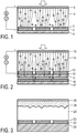
- Fig. 1 shows a schematic diagram of a radiation detector in accordance with an embodiment of the invention.
- the basic structure includes a substrate 1 with structured bottom electrodes 2 on it. On top of the bottom electrode 2 an electron blocking layer (not shown) might be present. On top of the arrangement of substrate 1 and bottom electrodes 2 a halide Perovskite layer 4 is placed, with a seeding layer 3 provided on the bottom electrodes 2.
- This layer 4 might be thin (100 nm -100 ⁇ m) for mammography, thicker (100 - 2000 ⁇ m) for general X-ray and CT and quite thick (1- 20 mm) for SPECT or PET.
- a hole blocking layer might (not shown) be present. Also might there be a conducting layer (not shown) to reduce/prevent shorts of a top electrode 5 towards the substrate 1.
- the top electrode 5 is deposited.
- the top electrode 5 might contain an electron injection layer (not shown).
- the total structure is a diode. This can be achieved by having different work functions between the bottom and the top electrodes 2, 5.
- the voltage applied on the total stack of layers should preferably put the diode in blocking mode to reduce dark current and increase the sensitivity and timing performance.
- An advantage of the inorganic-organic halide Perovskite materials is that the energy gap and the mobility can be easily adjusted by varying the metals, halogen atoms and/or the organic groups as well as layer morphologies and multilayer device structures.
- the stack of layers shown in Fig. 1 may be part of an imaging detector which consists of multiple pixels.
- the formation of the pixels can be done only at one or multiple parts of the layer stack, wherein, for example, the X-ray absorption layer (Perovskite material) can be segmented with gaps or isolating layers in between the pixels, and/or on a continuous absorption layer one or both electrodes can be segmented.
- the X-ray absorption layer Perovskite material
- Fig. 2 shows a schematic partial diagram of a radiation detector in accordance with another embodiment of the invention.
- the Perovskite material(s) may be used also as light emitter to detect with good time resolution the signal with an extra photodetector and to measure the X-ray signal with good spatial resolution using the Perovskite material(s) as a direct conversion photoconductor.
- the photodetector is preferably a sufficiently fast photodetector. It is also possible to use a silicon photo-multiplier (SiPM).
- the arrangement of substrate 11, bottom electrode 12, seeding layer 13, Perovskite layer 14 and top electrode 15 basically corresponds to the corresponding arrangement shown in Fig. 1 .
- elements 16 for detection of the light emission are placed below the electrodes 12 for the direct conversion detection (i.e. electrodes 12 are used for direct conversion, while elements 16 are for scintillation light detection).
- a (semi-)transparent electrode material is used for electrodes 12.
- the photo-detectors 16 placed on a base 17 are optimized to operate for the wavelength emitted by the conversion material in this mode. For, for example, CH 3 NH 3 PbI 3 this would be in the infra-red part of the electromagnetic (EM) spectrum.
- the light absorption of the conversion material should preferably be mainly at other parts of the EM spectrum in such case to avoid self-absorption of the light emitted.
- the photo-detectors 16 are larger than the electrodes 12 in order to measure the emitted light with high geometrical fill factor.
- the photo-detectors may be large detection elements that are common for a number of bottom electrodes. This allows getting the time stamp of the scintillation light, while the corresponding charge would be detected with high spatial resolution on electrodes 12.
- Fig. 3 shows a further schematic partial diagram illustrating a layer structure in accordance with a further embodiment of the invention, which is quite similar to the structure illustrated in Fig. 1 and Fig. 2 .
- a laterally built-up diode may be provided.
- a thick CH 3 NH 3 PbI 3 Perovskite layer 24 can be grown by first providing a relatively thin CH 3 NH 3 PbBr 3 layer 23 in a structured manner (e.g. by inkjet) on a glass substrate 21 on which bottom electrodes 22 are provided (it is also possible to provide the seeding layer 23 is an unstructured manner, e.g. by spin-coating).
- a planarizing electron injection layer 26 (an example of a charge blocking layer) is provided.
- Fig. 1 and Fig. 2 include the seeding layers 3 and 13, respectively, in correspondence to the CH 3 NH 3 PbBr 3 layer 23.
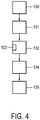
- Fig. 4 shows a flow diagram illustrating step of the method according to an embodiment of the invention.
- desired portions thereof are roughened in roughening step 100 in order to enhance the contact stability between the deposited CH 3 NH 3 PbBr 3 layer.
- a CH 3 NH 3 PbBr 3 layer is provided as a seeding layer.
- a layer growth step 102 is provided, in which the detector layer including CH 3 NH 3 PbI 3 as inorganic-organic halide Perovskite material is provided, as discussed above.
- the layer growth step includes in this case an inclusion substep 103 of including a light emission material in the detector layer.
- a planarizing step 104 in which a planarizing layer in form of a charge blocking layer is provided.
- the radiation detector may be provided with photo detectors (see Fig. 2 ), in order to provide a combined direct and indirect detection.
- Additional (light) emitter materials may be incorporated and distributed in the active Perovskite layer(s).
- the Perovskite material may absorb X-ray and may transfer part of the absorbed energy to the additional emitter material.
- This emitter material might then emit the light preferably having a wavelength outside of the absorption band of the Perovskite material(s). This light can then be detected by a photo-detector.
- the present invention includes the use of methyl ammonium lead halide Perovskites (CH 3 NH 3 Pb(I/Br/Cl) 3 ) as a semiconductor photo-detector material.
- Lead-free detectors may be provided by replacing the Pb components by Sn in the Perovskites materials (CH 3 NH 3 Sn(I/Br/Cl) 3 ). The resulting detector has less environmental issues than one including Pb.
- Perovskite material(s) by locally depositing by e.g. inkjet of the thin layer of, for example, CH 3 NH 3 PbBr 3 on an oxidic/metallic conductor on which, for example, CH 3 NH 3 PbI 3 would not grow by itself to a satisfactory amount.
- a surface roughening might be provided.
- another approach may include selectively depositing a non-sticking layer like SiO 2 to achieve or enhance selective growth of, for example, the CH 3 NH 3 PbI 3 .
- the present invention may be implemented also by using organic substrates. If the organic layers are not conductive, this crystal growth is then more suited for scintillators.
- the present invention may particularly be employed to benefit in the areas of mammography, CT, PET scanners (including multimodal), nuclear medicine (planar cameras, SPECT), safety (e.g. nuclear plants and environment), security, particle and high energy physics, non-destructive inspection, astrophysics and hunting for (mineral) resources, even though this list in not exhaustive.
- a single processor, device or other unit may fulfill the functions of several items recited in the claims.
- the mere fact that certain measures are recited in mutually different dependent claims does not indicate that a combination of these measures cannot be used to advantage.
Landscapes
- Physics & Mathematics (AREA)
- Health & Medical Sciences (AREA)
- Life Sciences & Earth Sciences (AREA)
- General Physics & Mathematics (AREA)
- High Energy & Nuclear Physics (AREA)
- Molecular Biology (AREA)
- Spectroscopy & Molecular Physics (AREA)
- Chemical & Material Sciences (AREA)
- Electromagnetism (AREA)
- Engineering & Computer Science (AREA)
- Materials Engineering (AREA)
- Crystallography & Structural Chemistry (AREA)
- Manufacturing & Machinery (AREA)
- Measurement Of Radiation (AREA)
- Light Receiving Elements (AREA)
- Luminescent Compositions (AREA)
Claims (15)
- Verfahren zur Herstellung eines Strahlungsdetektors für ionisierende Strahlung mit einem ersten anorganisch-organischen Halogenid-Perowskit-Material als Direktkonvertermaterial und/oder als Szintillatormaterial in einer Detektorschicht (4, 14, 24), umfassend:einen Impfschritt (101) zum Bereitstellen einer Impfschicht (3, 13, 23), die ein zweites anorganischorganisches Halogenid-Perowskitmaterial enthält, das sich von dem ersten anorganisch-organischen Halogenid-Perowskitmaterial unterscheidet, undeinen Schichtwachstumsschritt (102) zum Bilden der Detektorschicht (4, 14, 24) durch Aufwachsen des ersten anorganisch-organischen Halogenid-Perowskitmaterials aus einer Lösung auf der Impfschicht (3, 13, 23).
- Verfahren nach Anspruch 1,
wobei die ersten und zweiten anorganisch-organischen Halogenid-Perowskitmaterialien aus Methylammoniummetallhalogenid und/oder Formamidiniummetallhalogenid bestehen oder diese umfassen. - Verfahren nach Anspruch 2,
wobei das Metallhalogenid ein Bleihalogenid oder ein Zinnhalogenid ist. - Verfahren nach Anspruch 3,
wobei das erste anorganisch-organische Halogenid-Perowskit-Material aus einem Iodid besteht oder dieses umfasst und das zweite anorganisch-organische Halogenid-Perowskit-Material aus einem Bromid besteht oder dieses umfasst. - Verfahren nach Anspruch 4,
wobei die Lösung eine Mischung aus einer Metallacetat/Iodwasserstoff-Lösung und einer Methylamin/Iodwasserstoff-Lösung ist. - Verfahren nach Anspruch 1,
wobei in dem Schichtwachstumsschritt (102) ein Lichtemissionsmaterial (103) in der Detektorschicht (14) enthalten ist. - Verfahren nach Anspruch 6,
wobei das Lichtemissionsmaterial lumineszierende Quantenpunkte und/oder Phosphorpartikel umfasst. - Verfahren nach Anspruch 1,
wobei der Schichtwachstumsschritt (102) so vorgesehen ist, dass die Detektorschicht eine Dicke von 10 µm oder mehr aufweist. - Verfahren nach Anspruch 1,
ferner umfassend einen Planarisierungsschritt (104) des Bereitstellens einer planarisierenden Ladungsblockierungsschicht (26) auf der Detektorschicht (24). - Verfahren nach Anspruch 1, ferner umfassend
einen Bereitstellungsschritt (101) des Bereitstellens einer Struktur der Impfschicht (3, 13, 23) durch lokalisierte Abscheidung des zweiten anorganisch-organischen Halogenid-PerowskitMaterials, vorzugsweise durch Tintenstrahl-, Schlitzdüsen- und/oder Siebdruck. - Verfahren nach Anspruch 10, ferner umfassend:
einen Aufrauungsschritt (100) zum Aufrauen einer Oberfläche eines Substrats, auf dem die Impfschicht abgeschieden werden soll, vor dem Bereitstellungsschritt (101). - Strahlungsdetektor zur Detektion ionisierender Strahlung, umfassend eine Detektorschicht (4, 14, 24), wobei der Strahlungsdetektor mittels der Schritte des Verfahrens nach Anspruch 1 hergestellt ist, wobei der Strahlungsdetektor die Impfschicht (3, 13, 23) umfasst, die das zweite anorganisch-organischen Halogenid-Perowskitmaterials enthalt, das sich von dem ersten anorganisch-organischen Halogenid-Perowskitmaterial unterscheidet, und die Detektorschicht (4, 14, 24), die durch Aufwachsen des ersten anorganisch-organischen Halogenid-Perowskitmaterials aus einem Lösung auf der Impfschicht (3, 13, 23) gebildet ist.
- Strahlungsdetektor nach Anspruch 12, umfassend:- ein Substrat (1, 11, 21), eine strukturierte Vielzahl von unteren Elektroden (2, 12, 22), die Detektorschicht (4, 14, 24) und eine obere Elektrode (5, 15, 25) in dieser Reihenfolge, wobei auf jeder der unteren Elektroden (2, 12, 22) ein Teil der Impfschicht (3, 13, 23) vorgesehen ist, oder- ein Substrat (1, 11, 21), eine strukturierte Vielzahl von Elektroden (2, 12, 22) und die Detektorschicht (4, 14, 24) in dieser Reihenfolge, wobei auf jeder der Elektroden (2, 12, 22) ein Teil der Impfschicht (3, 13, 23) bereitgestellt wird und die Elektroden (2, 12, 22) Anoden und Kathoden umfassen.
- Strahlungsdetektor nach Anspruch 13, mit einer Ladungsblockierungsschicht zwischen den unteren Elektroden (2, 12, 22) und der Detektorschicht (4, 14, 24), zwischen den Anoden und Kathoden (2, 12, 22) und die Detektorschicht (4, 14, 24) und/oder eine Ladungsblockierungsschicht (26) und/oder eine leitende Schicht zwischen der Detektorschicht (4, 14, 24) und der oberen Elektrode (5, 15, 25).
- Strahlungsdetektor nach Anspruch 13, ferner umfassend eine Vielzahl von Fotodetektoren (16), die so angeordnet sind, dass sie die unteren Elektroden (12) oder die Anoden und Kathoden mit dem Detektormaterial (14) sandwichartig einschließen, wobei die Fotodetektoren (16) konfiguriert sind, um eine durch eine einfallende Strahlung verursachte Lichtemission des Detektormaterials (14) zu detektieren.
Applications Claiming Priority (2)
| Application Number | Priority Date | Filing Date | Title |
|---|---|---|---|
| EP15185586 | 2015-09-17 | ||
| PCT/EP2016/072065 WO2017046390A1 (en) | 2015-09-17 | 2016-09-16 | Method for producing a radiation detector and radiation detector |
Publications (2)
| Publication Number | Publication Date |
|---|---|
| EP3350836A1 EP3350836A1 (de) | 2018-07-25 |
| EP3350836B1 true EP3350836B1 (de) | 2021-11-10 |
Family
ID=54151115
Family Applications (1)
| Application Number | Title | Priority Date | Filing Date |
|---|---|---|---|
| EP16767258.3A Active EP3350836B1 (de) | 2015-09-17 | 2016-09-16 | Verfahren zur herstellung eines strahlungsdetektors sowie strahlungsdetektor |
Country Status (5)
| Country | Link |
|---|---|
| US (1) | US10573690B2 (de) |
| EP (1) | EP3350836B1 (de) |
| JP (1) | JP6960907B2 (de) |
| CN (1) | CN108028263B (de) |
| WO (1) | WO2017046390A1 (de) |
Families Citing this family (21)
| Publication number | Priority date | Publication date | Assignee | Title |
|---|---|---|---|---|
| EP3232229A1 (de) * | 2016-04-13 | 2017-10-18 | Nokia Technologies Oy | Vorrichtung zur erfassung von strahlung |
| CA3037960A1 (en) * | 2016-11-30 | 2018-06-07 | The Research Foundation For The State University Of New York | Hybrid active matrix flat panel detector system and method |
| US11940577B1 (en) * | 2017-10-19 | 2024-03-26 | Radiation Monitoring Devices, Inc. | Wide bandgap semiconductor radiation detectors |
| JP6975079B2 (ja) * | 2018-03-15 | 2021-12-01 | 株式会社東芝 | 放射線検出器 |
| CN108649127A (zh) * | 2018-05-17 | 2018-10-12 | 北京大学 | 一种基于种子层辅助生长的连续多层钙钛矿薄膜制备方法 |
| DE112019003191T5 (de) * | 2018-06-26 | 2021-04-29 | Hamamatsu Photonics K.K. | Strahlungsdetektor und Verfahren zum Herstellen von Strahlungsdetektor |
| US11824132B2 (en) | 2019-04-29 | 2023-11-21 | King Abdullah University Of Science And Technology | Indirect bandgap, perovskite-based X-ray detector and method |
| WO2020240947A1 (ja) * | 2019-05-29 | 2020-12-03 | パナソニックIpマネジメント株式会社 | 光電変換膜およびそれを用いた太陽電池、ならびに光電変換膜の製造方法 |
| CN110609313A (zh) * | 2019-09-30 | 2019-12-24 | 南华大学 | 轻便式γ辐射定向探测器 |
| EP3799787A1 (de) | 2019-10-01 | 2021-04-07 | Koninklijke Philips N.V. | Detektor für ein dunkelfeld-, phasenkontrast- und dämpfungsinterferometrie-bildgebungssystem |
| EP3863059B1 (de) * | 2020-02-04 | 2024-07-31 | Siemens Healthineers AG | Perowskit-basierte detektoren mit erhöhter adhäsion |
| EP3863054A1 (de) * | 2020-02-04 | 2021-08-11 | Siemens Healthcare GmbH | Multiple spektrale detektoren mittels strukturierter perowskite |
| JPWO2022030154A1 (de) * | 2020-08-06 | 2022-02-10 | ||
| CN111965689B (zh) * | 2020-08-12 | 2021-04-09 | 中国科学院国家空间科学中心 | 一种用于中性原子分析的测量装置 |
| CN111948696B (zh) * | 2020-08-13 | 2023-04-18 | 京东方科技集团股份有限公司 | 射线探测器基板、射线探测器及射线探测方法 |
| FR3116153A1 (fr) | 2020-11-09 | 2022-05-13 | Commissariat A L'energie Atomique Et Aux Energies Alternatives | Procédé de fabrication orientée d’un cristal de conversion par voie liquide |
| EP4068363B1 (de) * | 2021-03-30 | 2023-06-07 | Siemens Healthcare GmbH | Strahlungsdetektor mit gestossenen absorberkacheln ohne tote bereiche |
| CN113219518A (zh) * | 2021-05-08 | 2021-08-06 | 西北核技术研究所 | 一种基于富氢钙钛矿闪烁体的辐射探测装置及探测方法 |
| CN113433580B (zh) * | 2021-06-25 | 2023-03-10 | 中国科学技术大学 | 气体探测器制作方法、气体探测器及射线探测装置 |
| EP4270512A1 (de) | 2022-04-25 | 2023-11-01 | Fundacja Saule Research Institute | Perowskitstruktur, photovoltaische zelle und verfahren zu ihrer herstellung |
| CN114937708B (zh) * | 2022-05-25 | 2024-04-16 | 华中科技大学 | 一种全钙钛矿x射线间接探测器及其制备方法 |
Family Cites Families (13)
| Publication number | Priority date | Publication date | Assignee | Title |
|---|---|---|---|---|
| DE4002429A1 (de) | 1990-01-27 | 1991-08-01 | Philips Patentverwaltung | Sensormatrix |
| US5961714A (en) * | 1996-03-07 | 1999-10-05 | Schlumberger Technology Corporation | Method of growing lutetium aluminum perovskite crystals and apparatus including lutetium aluminum perovskite crystal scintillators |
| JP3779604B2 (ja) * | 2001-01-15 | 2006-05-31 | 独立行政法人科学技術振興機構 | 放射線検出装置 |
| JP2002365368A (ja) | 2001-06-04 | 2002-12-18 | Anritsu Corp | X線検出器及び該検出器を用いたx線異物検出装置 |
| US20030015704A1 (en) * | 2001-07-23 | 2003-01-23 | Motorola, Inc. | Structure and process for fabricating semiconductor structures and devices utilizing the formation of a compliant substrate for materials used to form the same including intermediate surface cleaning |
| JP3714918B2 (ja) | 2001-07-31 | 2005-11-09 | 独立行政法人科学技術振興機構 | 放射線検出装置 |
| JP2006170827A (ja) * | 2004-12-16 | 2006-06-29 | Japan Science & Technology Agency | 放射線検出用シンチレーター |
| US7569109B2 (en) * | 2006-08-23 | 2009-08-04 | General Electric Company | Single crystal scintillator materials and methods for making the same |
| WO2013067502A1 (en) * | 2011-11-04 | 2013-05-10 | University Of Houston System | System and method for monolithic crystal growth |
| ES2924644T3 (es) * | 2012-09-18 | 2022-10-10 | Univ Oxford Innovation Ltd | Dispositivo optoelectrónico |
| TWI485154B (zh) * | 2013-05-09 | 2015-05-21 | Univ Nat Cheng Kung | 具鈣鈦礦結構吸光材料之有機混成太陽能電池及其製造方法 |
| US9416279B2 (en) * | 2013-11-26 | 2016-08-16 | Hunt Energy Enterprises, L.L.C. | Bi- and tri-layer interfacial layers in perovskite material devices |
| CN103700769B (zh) * | 2013-12-03 | 2016-05-04 | 常州大学 | 一种有机/无机杂化钙钛矿太阳能电池及其制备方法 |
-
2016
- 2016-09-16 CN CN201680053905.2A patent/CN108028263B/zh active Active
- 2016-09-16 JP JP2018512400A patent/JP6960907B2/ja active Active
- 2016-09-16 EP EP16767258.3A patent/EP3350836B1/de active Active
- 2016-09-16 WO PCT/EP2016/072065 patent/WO2017046390A1/en active Application Filing
- 2016-09-16 US US15/760,645 patent/US10573690B2/en active Active
Also Published As
| Publication number | Publication date |
|---|---|
| CN108028263B (zh) | 2022-10-21 |
| CN108028263A (zh) | 2018-05-11 |
| JP2018535537A (ja) | 2018-11-29 |
| EP3350836A1 (de) | 2018-07-25 |
| WO2017046390A1 (en) | 2017-03-23 |
| US20180277608A1 (en) | 2018-09-27 |
| JP6960907B2 (ja) | 2021-11-05 |
| US10573690B2 (en) | 2020-02-25 |
Similar Documents
| Publication | Publication Date | Title |
|---|---|---|
| EP3350836B1 (de) | Verfahren zur herstellung eines strahlungsdetektors sowie strahlungsdetektor | |
| Wu et al. | Metal halide perovskites for X-ray detection and imaging | |
| Xu et al. | High-performance surface barrier X-ray detector based on methylammonium lead tribromide single crystals | |
| Liu et al. | Recent progress in halide perovskite radiation detectors for gamma-ray spectroscopy | |
| US10656290B2 (en) | Direct photon conversion detector | |
| US8735839B2 (en) | Pastes for photoelectric conversion layers of X-ray detectors, X-ray detectors and methods of manufacturing the same | |
| US20110049379A1 (en) | Neutron detectors made of inorganic materials and their method of fabrication | |
| Zhang et al. | A flat panel photodetector formed by a ZnS photoconductor and ZnO nanowire field emitters achieving high responsivity from ultraviolet to visible light for indirect-conversion X-ray imaging | |
| JP2019537738A (ja) | 直接変換型放射線検出器 | |
| US9632190B2 (en) | Neutron imaging systems utilizing lithium-containing semiconductor crystals | |
| Peng et al. | X-ray detection based on crushed perovskite crystal/polymer composites | |
| Isshiki et al. | II-IV semiconductors for optoelectronics: CdS, CdSe, CdTe | |
| US9429662B2 (en) | Bulk semiconducting scintillator device for radiation detection | |
| CN113257847A (zh) | 一种钙钛矿各向异性增强的高分辨率伽马射线成像方法 | |
| Zou et al. | Pixellated perovskite photodiode on IGZO thin film transistor backplane for low dose indirect X-ray detection | |
| WO2015148544A1 (en) | Compact solid-state neutron detector | |
| Gedda et al. | Metal Halide Perovskites for High-Energy Radiation Detection | |
| US9612345B2 (en) | Visible scintillation photodetector device incorporating chalcopyrite semiconductor crystals | |
| Yangbing et al. | On-Substrate Grown MAPbBr 3 Single Crystal Diodes for Large-Area and Low-Dark-Current X-Ray Detection | |
| Li et al. | Radiation detection technologies enabled by halide perovskite single crystals | |
| CN221429476U (zh) | 一种高效率高能光子探测器 | |
| WO2022030156A1 (ja) | 電離放射線変換デバイス、電離放射線の検出方法、及び電離放射線変換デバイスの製造方法 | |
| Fernandez-Izquierdo et al. | Halide Perovskite Thin Films for Neutron and X-Ray Detection | |
| EP3730972A1 (de) | Strahlungsdetektionsvorrichtung zur detektion von gamma- oder röntgenstrahlungsquanten | |
| Andričević | The impact of detection volume on hybrid halide perovskite-based radiation detectors |
Legal Events
| Date | Code | Title | Description |
|---|---|---|---|
| STAA | Information on the status of an ep patent application or granted ep patent |
Free format text: STATUS: UNKNOWN |
|
| STAA | Information on the status of an ep patent application or granted ep patent |
Free format text: STATUS: THE INTERNATIONAL PUBLICATION HAS BEEN MADE |
|
| PUAI | Public reference made under article 153(3) epc to a published international application that has entered the european phase |
Free format text: ORIGINAL CODE: 0009012 |
|
| STAA | Information on the status of an ep patent application or granted ep patent |
Free format text: STATUS: REQUEST FOR EXAMINATION WAS MADE |
|
| 17P | Request for examination filed |
Effective date: 20180417 |
|
| AK | Designated contracting states |
Kind code of ref document: A1 Designated state(s): AL AT BE BG CH CY CZ DE DK EE ES FI FR GB GR HR HU IE IS IT LI LT LU LV MC MK MT NL NO PL PT RO RS SE SI SK SM TR |
|
| AX | Request for extension of the european patent |
Extension state: BA ME |
|
| DAV | Request for validation of the european patent (deleted) | ||
| DAX | Request for extension of the european patent (deleted) | ||
| RAP1 | Party data changed (applicant data changed or rights of an application transferred) |
Owner name: KONINKLIJKE PHILIPS N.V. |
|
| GRAP | Despatch of communication of intention to grant a patent |
Free format text: ORIGINAL CODE: EPIDOSNIGR1 |
|
| STAA | Information on the status of an ep patent application or granted ep patent |
Free format text: STATUS: GRANT OF PATENT IS INTENDED |
|
| RIC1 | Information provided on ipc code assigned before grant |
Ipc: H01L 27/30 20060101AFI20210325BHEP Ipc: G01T 1/20 20060101ALI20210325BHEP Ipc: G01T 1/24 20060101ALI20210325BHEP Ipc: H01L 51/48 20060101ALN20210325BHEP |
|
| INTG | Intention to grant announced |
Effective date: 20210423 |
|
| GRAS | Grant fee paid |
Free format text: ORIGINAL CODE: EPIDOSNIGR3 |
|
| GRAA | (expected) grant |
Free format text: ORIGINAL CODE: 0009210 |
|
| STAA | Information on the status of an ep patent application or granted ep patent |
Free format text: STATUS: THE PATENT HAS BEEN GRANTED |
|
| AK | Designated contracting states |
Kind code of ref document: B1 Designated state(s): AL AT BE BG CH CY CZ DE DK EE ES FI FR GB GR HR HU IE IS IT LI LT LU LV MC MK MT NL NO PL PT RO RS SE SI SK SM TR |
|
| REG | Reference to a national code |
Ref country code: GB Ref legal event code: FG4D |
|
| REG | Reference to a national code |
Ref country code: AT Ref legal event code: REF Ref document number: 1446877 Country of ref document: AT Kind code of ref document: T Effective date: 20211115 Ref country code: CH Ref legal event code: EP |
|
| REG | Reference to a national code |
Ref country code: DE Ref legal event code: R096 Ref document number: 602016066046 Country of ref document: DE |
|
| REG | Reference to a national code |
Ref country code: IE Ref legal event code: FG4D |
|
| REG | Reference to a national code |
Ref country code: LT Ref legal event code: MG9D |
|
| REG | Reference to a national code |
Ref country code: NL Ref legal event code: MP Effective date: 20211110 |
|
| REG | Reference to a national code |
Ref country code: AT Ref legal event code: MK05 Ref document number: 1446877 Country of ref document: AT Kind code of ref document: T Effective date: 20211110 |
|
| PG25 | Lapsed in a contracting state [announced via postgrant information from national office to epo] |
Ref country code: RS Free format text: LAPSE BECAUSE OF FAILURE TO SUBMIT A TRANSLATION OF THE DESCRIPTION OR TO PAY THE FEE WITHIN THE PRESCRIBED TIME-LIMIT Effective date: 20211110 Ref country code: LT Free format text: LAPSE BECAUSE OF FAILURE TO SUBMIT A TRANSLATION OF THE DESCRIPTION OR TO PAY THE FEE WITHIN THE PRESCRIBED TIME-LIMIT Effective date: 20211110 Ref country code: FI Free format text: LAPSE BECAUSE OF FAILURE TO SUBMIT A TRANSLATION OF THE DESCRIPTION OR TO PAY THE FEE WITHIN THE PRESCRIBED TIME-LIMIT Effective date: 20211110 Ref country code: BG Free format text: LAPSE BECAUSE OF FAILURE TO SUBMIT A TRANSLATION OF THE DESCRIPTION OR TO PAY THE FEE WITHIN THE PRESCRIBED TIME-LIMIT Effective date: 20220210 Ref country code: AT Free format text: LAPSE BECAUSE OF FAILURE TO SUBMIT A TRANSLATION OF THE DESCRIPTION OR TO PAY THE FEE WITHIN THE PRESCRIBED TIME-LIMIT Effective date: 20211110 |
|
| PG25 | Lapsed in a contracting state [announced via postgrant information from national office to epo] |
Ref country code: IS Free format text: LAPSE BECAUSE OF FAILURE TO SUBMIT A TRANSLATION OF THE DESCRIPTION OR TO PAY THE FEE WITHIN THE PRESCRIBED TIME-LIMIT Effective date: 20220310 Ref country code: SE Free format text: LAPSE BECAUSE OF FAILURE TO SUBMIT A TRANSLATION OF THE DESCRIPTION OR TO PAY THE FEE WITHIN THE PRESCRIBED TIME-LIMIT Effective date: 20211110 Ref country code: PT Free format text: LAPSE BECAUSE OF FAILURE TO SUBMIT A TRANSLATION OF THE DESCRIPTION OR TO PAY THE FEE WITHIN THE PRESCRIBED TIME-LIMIT Effective date: 20220310 Ref country code: PL Free format text: LAPSE BECAUSE OF FAILURE TO SUBMIT A TRANSLATION OF THE DESCRIPTION OR TO PAY THE FEE WITHIN THE PRESCRIBED TIME-LIMIT Effective date: 20211110 Ref country code: NO Free format text: LAPSE BECAUSE OF FAILURE TO SUBMIT A TRANSLATION OF THE DESCRIPTION OR TO PAY THE FEE WITHIN THE PRESCRIBED TIME-LIMIT Effective date: 20220210 Ref country code: NL Free format text: LAPSE BECAUSE OF FAILURE TO SUBMIT A TRANSLATION OF THE DESCRIPTION OR TO PAY THE FEE WITHIN THE PRESCRIBED TIME-LIMIT Effective date: 20211110 Ref country code: LV Free format text: LAPSE BECAUSE OF FAILURE TO SUBMIT A TRANSLATION OF THE DESCRIPTION OR TO PAY THE FEE WITHIN THE PRESCRIBED TIME-LIMIT Effective date: 20211110 Ref country code: HR Free format text: LAPSE BECAUSE OF FAILURE TO SUBMIT A TRANSLATION OF THE DESCRIPTION OR TO PAY THE FEE WITHIN THE PRESCRIBED TIME-LIMIT Effective date: 20211110 Ref country code: GR Free format text: LAPSE BECAUSE OF FAILURE TO SUBMIT A TRANSLATION OF THE DESCRIPTION OR TO PAY THE FEE WITHIN THE PRESCRIBED TIME-LIMIT Effective date: 20220211 Ref country code: ES Free format text: LAPSE BECAUSE OF FAILURE TO SUBMIT A TRANSLATION OF THE DESCRIPTION OR TO PAY THE FEE WITHIN THE PRESCRIBED TIME-LIMIT Effective date: 20211110 |
|
| PG25 | Lapsed in a contracting state [announced via postgrant information from national office to epo] |
Ref country code: SM Free format text: LAPSE BECAUSE OF FAILURE TO SUBMIT A TRANSLATION OF THE DESCRIPTION OR TO PAY THE FEE WITHIN THE PRESCRIBED TIME-LIMIT Effective date: 20211110 Ref country code: SK Free format text: LAPSE BECAUSE OF FAILURE TO SUBMIT A TRANSLATION OF THE DESCRIPTION OR TO PAY THE FEE WITHIN THE PRESCRIBED TIME-LIMIT Effective date: 20211110 Ref country code: RO Free format text: LAPSE BECAUSE OF FAILURE TO SUBMIT A TRANSLATION OF THE DESCRIPTION OR TO PAY THE FEE WITHIN THE PRESCRIBED TIME-LIMIT Effective date: 20211110 Ref country code: EE Free format text: LAPSE BECAUSE OF FAILURE TO SUBMIT A TRANSLATION OF THE DESCRIPTION OR TO PAY THE FEE WITHIN THE PRESCRIBED TIME-LIMIT Effective date: 20211110 Ref country code: DK Free format text: LAPSE BECAUSE OF FAILURE TO SUBMIT A TRANSLATION OF THE DESCRIPTION OR TO PAY THE FEE WITHIN THE PRESCRIBED TIME-LIMIT Effective date: 20211110 Ref country code: CZ Free format text: LAPSE BECAUSE OF FAILURE TO SUBMIT A TRANSLATION OF THE DESCRIPTION OR TO PAY THE FEE WITHIN THE PRESCRIBED TIME-LIMIT Effective date: 20211110 |
|
| REG | Reference to a national code |
Ref country code: DE Ref legal event code: R097 Ref document number: 602016066046 Country of ref document: DE |
|
| PLBE | No opposition filed within time limit |
Free format text: ORIGINAL CODE: 0009261 |
|
| STAA | Information on the status of an ep patent application or granted ep patent |
Free format text: STATUS: NO OPPOSITION FILED WITHIN TIME LIMIT |
|
| 26N | No opposition filed |
Effective date: 20220811 |
|
| PG25 | Lapsed in a contracting state [announced via postgrant information from national office to epo] |
Ref country code: AL Free format text: LAPSE BECAUSE OF FAILURE TO SUBMIT A TRANSLATION OF THE DESCRIPTION OR TO PAY THE FEE WITHIN THE PRESCRIBED TIME-LIMIT Effective date: 20211110 |
|
| REG | Reference to a national code |
Ref country code: DE Ref legal event code: R079 Ref document number: 602016066046 Country of ref document: DE Free format text: PREVIOUS MAIN CLASS: H01L0027300000 Ipc: H10K0039000000 |
|
| PG25 | Lapsed in a contracting state [announced via postgrant information from national office to epo] |
Ref country code: SI Free format text: LAPSE BECAUSE OF FAILURE TO SUBMIT A TRANSLATION OF THE DESCRIPTION OR TO PAY THE FEE WITHIN THE PRESCRIBED TIME-LIMIT Effective date: 20211110 |
|
| PG25 | Lapsed in a contracting state [announced via postgrant information from national office to epo] |
Ref country code: MC Free format text: LAPSE BECAUSE OF FAILURE TO SUBMIT A TRANSLATION OF THE DESCRIPTION OR TO PAY THE FEE WITHIN THE PRESCRIBED TIME-LIMIT Effective date: 20211110 |
|
| REG | Reference to a national code |
Ref country code: CH Ref legal event code: PL |
|
| GBPC | Gb: european patent ceased through non-payment of renewal fee |
Effective date: 20220916 |
|
| REG | Reference to a national code |
Ref country code: BE Ref legal event code: MM Effective date: 20220930 |
|
| PG25 | Lapsed in a contracting state [announced via postgrant information from national office to epo] |
Ref country code: IT Free format text: LAPSE BECAUSE OF FAILURE TO SUBMIT A TRANSLATION OF THE DESCRIPTION OR TO PAY THE FEE WITHIN THE PRESCRIBED TIME-LIMIT Effective date: 20211110 |
|
| PG25 | Lapsed in a contracting state [announced via postgrant information from national office to epo] |
Ref country code: LU Free format text: LAPSE BECAUSE OF NON-PAYMENT OF DUE FEES Effective date: 20220916 |
|
| PG25 | Lapsed in a contracting state [announced via postgrant information from national office to epo] |
Ref country code: LI Free format text: LAPSE BECAUSE OF NON-PAYMENT OF DUE FEES Effective date: 20220930 Ref country code: IE Free format text: LAPSE BECAUSE OF NON-PAYMENT OF DUE FEES Effective date: 20220916 Ref country code: CH Free format text: LAPSE BECAUSE OF NON-PAYMENT OF DUE FEES Effective date: 20220930 |
|
| PG25 | Lapsed in a contracting state [announced via postgrant information from national office to epo] |
Ref country code: BE Free format text: LAPSE BECAUSE OF NON-PAYMENT OF DUE FEES Effective date: 20220930 |
|
| PG25 | Lapsed in a contracting state [announced via postgrant information from national office to epo] |
Ref country code: GB Free format text: LAPSE BECAUSE OF NON-PAYMENT OF DUE FEES Effective date: 20220916 |
|
| PGFP | Annual fee paid to national office [announced via postgrant information from national office to epo] |
Ref country code: FR Payment date: 20230926 Year of fee payment: 8 Ref country code: DE Payment date: 20230928 Year of fee payment: 8 |
|
| REG | Reference to a national code |
Ref country code: DE Ref legal event code: R084 Ref document number: 602016066046 Country of ref document: DE |
|
| PG25 | Lapsed in a contracting state [announced via postgrant information from national office to epo] |
Ref country code: HU Free format text: LAPSE BECAUSE OF FAILURE TO SUBMIT A TRANSLATION OF THE DESCRIPTION OR TO PAY THE FEE WITHIN THE PRESCRIBED TIME-LIMIT; INVALID AB INITIO Effective date: 20160916 |
|
| PG25 | Lapsed in a contracting state [announced via postgrant information from national office to epo] |
Ref country code: CY Free format text: LAPSE BECAUSE OF FAILURE TO SUBMIT A TRANSLATION OF THE DESCRIPTION OR TO PAY THE FEE WITHIN THE PRESCRIBED TIME-LIMIT Effective date: 20211110 |
|
| PG25 | Lapsed in a contracting state [announced via postgrant information from national office to epo] |
Ref country code: MK Free format text: LAPSE BECAUSE OF FAILURE TO SUBMIT A TRANSLATION OF THE DESCRIPTION OR TO PAY THE FEE WITHIN THE PRESCRIBED TIME-LIMIT Effective date: 20211110 |
|
| PG25 | Lapsed in a contracting state [announced via postgrant information from national office to epo] |
Ref country code: MT Free format text: LAPSE BECAUSE OF FAILURE TO SUBMIT A TRANSLATION OF THE DESCRIPTION OR TO PAY THE FEE WITHIN THE PRESCRIBED TIME-LIMIT Effective date: 20211110 |