EP3345207B1 - Plasma-hf-vorspannungsunterdrückungssystem - Google Patents
Plasma-hf-vorspannungsunterdrückungssystem Download PDFInfo
- Publication number
- EP3345207B1 EP3345207B1 EP16842760.7A EP16842760A EP3345207B1 EP 3345207 B1 EP3345207 B1 EP 3345207B1 EP 16842760 A EP16842760 A EP 16842760A EP 3345207 B1 EP3345207 B1 EP 3345207B1
- Authority
- EP
- European Patent Office
- Prior art keywords
- generator
- signal
- output
- power
- frequency
- Prior art date
- Legal status (The legal status is an assumption and is not a legal conclusion. Google has not performed a legal analysis and makes no representation as to the accuracy of the status listed.)
- Active
Links
Images



Classifications
-
- H—ELECTRICITY
- H01—ELECTRIC ELEMENTS
- H01J—ELECTRIC DISCHARGE TUBES OR DISCHARGE LAMPS
- H01J37/00—Discharge tubes with provision for introducing objects or material to be exposed to the discharge, e.g. for the purpose of examination or processing thereof
- H01J37/32—Gas-filled discharge tubes
- H01J37/32009—Arrangements for generation of plasma specially adapted for examination or treatment of objects, e.g. plasma sources
- H01J37/32082—Radio frequency generated discharge
- H01J37/32174—Circuits specially adapted for controlling the RF discharge
-
- H—ELECTRICITY
- H01—ELECTRIC ELEMENTS
- H01J—ELECTRIC DISCHARGE TUBES OR DISCHARGE LAMPS
- H01J37/00—Discharge tubes with provision for introducing objects or material to be exposed to the discharge, e.g. for the purpose of examination or processing thereof
- H01J37/32—Gas-filled discharge tubes
- H01J37/32009—Arrangements for generation of plasma specially adapted for examination or treatment of objects, e.g. plasma sources
- H01J37/32082—Radio frequency generated discharge
- H01J37/32091—Radio frequency generated discharge the radio frequency energy being capacitively coupled to the plasma
-
- H—ELECTRICITY
- H01—ELECTRIC ELEMENTS
- H01J—ELECTRIC DISCHARGE TUBES OR DISCHARGE LAMPS
- H01J37/00—Discharge tubes with provision for introducing objects or material to be exposed to the discharge, e.g. for the purpose of examination or processing thereof
- H01J37/32—Gas-filled discharge tubes
- H01J37/32009—Arrangements for generation of plasma specially adapted for examination or treatment of objects, e.g. plasma sources
- H01J37/32082—Radio frequency generated discharge
- H01J37/321—Radio frequency generated discharge the radio frequency energy being inductively coupled to the plasma
-
- H—ELECTRICITY
- H01—ELECTRIC ELEMENTS
- H01J—ELECTRIC DISCHARGE TUBES OR DISCHARGE LAMPS
- H01J37/00—Discharge tubes with provision for introducing objects or material to be exposed to the discharge, e.g. for the purpose of examination or processing thereof
- H01J37/32—Gas-filled discharge tubes
- H01J37/32009—Arrangements for generation of plasma specially adapted for examination or treatment of objects, e.g. plasma sources
- H01J37/32082—Radio frequency generated discharge
- H01J37/32137—Radio frequency generated discharge controlling of the discharge by modulation of energy
- H01J37/32155—Frequency modulation
-
- H—ELECTRICITY
- H01—ELECTRIC ELEMENTS
- H01J—ELECTRIC DISCHARGE TUBES OR DISCHARGE LAMPS
- H01J37/00—Discharge tubes with provision for introducing objects or material to be exposed to the discharge, e.g. for the purpose of examination or processing thereof
- H01J37/32—Gas-filled discharge tubes
- H01J37/32009—Arrangements for generation of plasma specially adapted for examination or treatment of objects, e.g. plasma sources
- H01J37/32082—Radio frequency generated discharge
- H01J37/32137—Radio frequency generated discharge controlling of the discharge by modulation of energy
- H01J37/32155—Frequency modulation
- H01J37/32165—Plural frequencies
-
- H—ELECTRICITY
- H01—ELECTRIC ELEMENTS
- H01J—ELECTRIC DISCHARGE TUBES OR DISCHARGE LAMPS
- H01J37/00—Discharge tubes with provision for introducing objects or material to be exposed to the discharge, e.g. for the purpose of examination or processing thereof
- H01J37/32—Gas-filled discharge tubes
- H01J37/32009—Arrangements for generation of plasma specially adapted for examination or treatment of objects, e.g. plasma sources
- H01J37/32082—Radio frequency generated discharge
- H01J37/32174—Circuits specially adapted for controlling the RF discharge
- H01J37/32183—Matching circuits
Definitions
- the present disclosure relates to RF control systems and to a RF control system to reduce impedance fluctuations in a load.
- Plasma etching is frequently used in semiconductor fabrication. In plasma etching, ions are accelerated by an electric field to etch exposed surfaces on a substrate. The electric field is generated based on RF power signals generated by a radio frequency (RF) generator of a RF power system. The RF power signals generated by the RF generator must be precisely controlled to effectively execute plasma etching.
- RF radio frequency
- a RF power system may include a RF generator or supply, a matching network, and a load (e.g., a plasma chamber).
- the RF generator generates RF power signals, which are received at the matching network.
- the matching network matches an input impedance of the matching network to a characteristic impedance of a transmission line between the RF generator and the matching network. This impedance matching aids in maximizing an amount of power forwarded to the matching network ("forward power") and minimizing an amount of power reflected back from the matching network to the RF generator (“reverse power"). Forward power may be maximized and reverse power may be minimized when the input impedance of the matching network matches the characteristic impedance of the transmission line.
- output power applied to the load is determined by using sensors that measure the forward and reflected power or the voltage and current of the RF signal applied to the load. Either set of these signals is analyzed to determine the parameters of the power applied to the load.
- the parameters can include, for example, voltage, current, frequency, and phase.
- the analysis typically determines a power value which is used to adjust the output of the RF power supply in order to vary the power applied to the load.
- the varying impedance of the load causes a corresponding varying power applied to the load, as applied power is in part a function of the impedance of the load. Therefore, the varying impedance can necessitate varying the parameters of the power applied to the load in order to maintain optimum application of power from the RF power supply to the load.
- a first, more traditional approach is to apply a continuous wave signal to the load.
- the continuous wave signal is typically a sinusoidal wave that is output continuously by the power source to the load.
- the RF signal assumes a sinusoidal output, and the amplitude and/or frequency of the sinusoidal wave can be varied in order to vary the output power applied to the load.
- a second approach to applying the RF signal to the load involves pulsing the RF signal, rather than applying a continuous wave signal to the load.
- a RF sinusoidal signal is modulated by a modulation signal in order to define an envelope for the modulated sinusoidal signal.
- the RF sinusoidal signal typically is output at a constant frequency and amplitude. Power delivered to the load is varied by varying the modulation signal, rather than varying the sinusoidal, RF signal.
- power is typically delivered in one of two configurations.
- the power is capacitively coupled to the plasma chamber.
- CCP capacitively coupled plasma
- ICP inductively coupled plasma
- Plasma delivery systems typically include a bias and a source that apply respective bias power and source power to one or a plurality of electrodes.
- the source power typically generates a plasma within the plasma chamber, and the bias power tunes the plasma to an energy relative to the bias RF power supply.
- the bias and the source may share the same electrode or may use separate electrodes, in accordance with various design considerations.
- RF plasma processing systems include components for plasma generation and control.
- One such component is referred to as a plasma chamber or reactor.
- a typical plasma chamber or reactor utilized in RF plasma processing systems such as by way of example, for thin-film manufacturing, utilizes a dual frequency system.
- One frequency (the source) of the dual frequency system controls the generation of the plasma, and the other frequency (the bias) of the dual frequency system controls ion energy.
- RIE reactive-ion etching
- RIE is an etching technology used in microfabrication.
- RIE is typically characterized as dry etching.
- RIE uses a chemically reactive plasma to remove material deposited on wafers.
- the plasma is generated under low pressure (vacuum) by an electromagnetic field.
- High-energy ions from the plasma bombard the wafer surface and react with it to affect the etching process.
- a high frequency source RF power generator for example, 13 MHz - 100 MHz
- a lower frequency bias RF generator 100 kHz - 13 MHz
- the low frequency bias source introduces fluctuations in both the power and load impedance and into source RF generator.
- the plasma consists of a generally neutrally charged bulk region and a sheath region that oscillates near the surfaces of the vacuum chamber and substrate.
- the thickness of the sheath determines a significant portion of the plasma capacitance and is most affected by the low frequency bias power supply.
- the higher frequency source generator can be adversely affected by the sheath capacitance variation, resulting in large impedance and reflected power fluctuations. These fluctuations are usually too fast to be measured by present sensors and metrology systems.
- US 2006/232471 A1 describes phase and frequency control of a radio frequency generator from an external source.
- the RF generator includes a power source, a sensor, and a sensor signal processing unit.
- the sensor signal processing unit is coupled to the power source and to the sensor.
- the sensor signal processing unit controls the phase and/or the frequency of a RF generator.
- a radio frequency (RF) power delivery system includes a first RF generator and a second RF generator.
- the first RF generator operates as a master RF generator
- the second RF generator operates as a slave RF generator.
- the slave RF generator includes a detector for sensing an electrical characteristic of the RF signal of the slave RF generator.
- the slave RF generator also includes a detector for sensing an electrical characteristic of the RF signal from the master RF generator. Operation of the slave RF generator is controlled by a host or controller. The host or controller operates the slave RF generator in accordance with electrical properties determined by the second detector.
- a radio frequency generator includes a power control module, a frequency control module and a pulse generating module.
- the power control module is configured to generate a power signal indicating power levels for target states of a power amplifier.
- the frequency control module is configured to generate a frequency signal indicating frequencies for the target states of the power amplifier.
- the pulse generating module is configured to (i) supply an output signal to the power amplifier, (ii) recall at least one of a latest power level or a latest frequency for one of the target states of the power amplifier, and (iii) adjust a current power level and a current frequency of the output signal from a first state to a second state based on the power signal, the frequency signal, and at least one of the latest power level and the latest frequency of the power amplifier.
- US 2014/320013 A1 describes multiple radio frequency power supply control of frequency and phase.
- a system has a first RF generator and a second RF generator.
- the first RF generator controls the frequency of the second RF generator.
- the first RF generator includes a power source, a sensor, and a sensor signal processing unit.
- the sensor signal processing unit is coupled to the power source and to the sensor.
- the sensor signal processing unit scales the frequency of the first RF generator to control the frequency of the second RF generator.
- An RF supply system in which a first RF generator and a second RF generator provide respective RF output power signals to a load, such as a plasma chamber.
- a first RF generator and a second RF generator provide respective RF output power signals to a load, such as a plasma chamber.
- One of the first and second generators operates at a first frequency
- a second of the RF generators operates at a second frequency.
- One of the first and second generators detects a triggering event.
- the one of the first and second generators initiates adjusting the frequency of its RF output power signal in order to respond to impedance fluctuations in the plasma chamber that occur with respect to the triggering event.
- FIG. 1 depicts a RF generator or power supply system 10.
- Power supply system 10 includes a pair of radio frequency (RF) generators or power supplies 12a, 12b, matching networks 18a, 18b, and load or plasma chamber 32.
- RF generator 12a is referred to as a source RF generator
- matching network 18a is referred to as a source matching network.
- RF generator 12b is referred to as a bias RF generator
- matching network 18b is referred to as a bias matching network.
- Bias RF generator 12b generates a control signal 30 that is input to source RF generator 12a.
- control signal 30 includes information about the operation of bias RF generator 12b that enables predictive responsiveness to address fluctuations in the impedance of plasma chamber 32.
- RF generators 12a, 12b operate autonomously.
- RF generators 12a, 12b include respective RF power sources or amplifiers 14a, 14b, RF sensors 16a, 16b, and processors, controllers, or control modules 20a, 20b.
- RF power sources 14a, 14b generate respective RF power signals 22a, 22b output to respective sensors 16a, 16b.
- Sensors 16a, 16b receive the output of RF power sources 14a, 14b and generate respective RF power signals f 1 and f 2 .
- Sensors 16a, 16b also output signals that vary in accordance with various parameters sensed from load 32. While sensors 16a, 16b, are shown within respective RF generators 12a, 12b, it should be noted that RF sensors 16a, 16b can be located externally to the RF power generators 12a, 12b.
- Such external sensing can occur at the output of the RF generator, at the input of the impedance matching device that is located between the RF generator and the plasma chamber, or between the output of the impedance matching circuit (including, inside the impedance matching device) and the plasma chamber.
- Sensors 16a, 16b detect operating parameters of plasma chamber 32 and output signals X and Y.
- Sensors 16a, 16b may include voltage, current, and/or directional coupler sensors. Sensors 16a, 16b may detect (i) voltage V and current I and/or (ii) forward (or source) power P FWD output from respective power amplifiers 14a, 14b and/or RF generators 12a, 12b and reverse (or reflected) power P REV received from respective matching network 18a, 18b or a load 32 connected to respective sensors 16a, 16b.
- the voltage V, current I, forward power P FWD , and reverse power P REV may be scaled and/or filtered versions of the actual voltage, current, forward power, and reverse power associated with the respective power sources 14a, 14b.
- Sensors 16a, 16b may be analog and/or digital sensors.
- the sensors 16a, 16b may include analog-to-digital (A/D) converters and signal sampling components with corresponding sampling rates.
- Signals X and Y can represent any of the voltage V and current I or forward (or source) power P FWD reverse (or reflected) power P REV .
- Sensors 16a, 16b generate sensor signals X, Y, which are received by respective controllers or power control modules 20a, 20b.
- Power control modules 20a, 20b process the respective X, Y signals 24a, 26a and 24b, 26b and generate one or a plurality of feedback control signals to respective power sources 14a, 14b.
- Power sources 14a, 14b adjust the RF power signals 22a, 22b based on the received feedback control signal.
- Power control modules 20a, 20b may include at least, proportional integral derivative (PID) controllers or subsets thereof and/or direct digital synthesis (DDS) component(s) and/or any of the various components described below in connection with the term modules.
- PID proportional integral derivative
- DDS direct digital synthesis
- power control modules 20a, 20b are first PID controllers or subsets and may include functions, processes, processors, or submodules.
- Feedback control signals 28a, 28b may be drive signals and have a DC offset or rail voltage, voltage or current magnitude, a frequency, and a phase.
- RF power source 14a, sensor 16a, controller 20a, and match network 18a can be referred to as source RF power source 14a, source sensor 16a, source controller 20a, and source matching network 18a.
- RF power source 14b, sensor 16b, controller 20b, and match network 18b can be referred to as bias RF power source 14b, bias sensor 16b, bias controller 20b, and bias matching network 18b.
- the source term refers to the RF generator that generates the plasma
- the bias term refers to the RF generator that tunes the plasma Ion Energy Distribution Function (IEDF) relative to the bias RF power supply.
- the source and bias RF power supplies operate at different frequencies.
- the source RF power supply operates at a higher frequency than the bias RF power supply.
- source controller 20a adjusts the frequency of RF signal f 1 to compensate for impedance fluctuations resulting from the application of RF signal f 2 to plasma chamber 32.
- RF signal f 2 is a frequency lower than the frequency of RF signal f 1 .
- the lower frequency introduces intermodulation distortion (IMD), and the IMD causes impedance fluctuations in plasma chamber 32.
- IMD intermodulation distortion
- frequency offsets can be added to RF signal f 1 to compensate for the anticipated impedance fluctuations introduced by RF signal f 2 .
- the frequency offsets can be predetermined and stored in a lookup table, or the frequency offsets can be determined dynamically.
- Source controller 20a includes a playback module 34, a frequency offset module 36, and an update module 38.
- Each module 34, 36, 38 can be implemented collectively or individually as a process, a processor, a module, or a submodule. Further, each module 34, 36, 38 can be implemented as any of the various components described below in connection with the term module.
- Playback module 34 monitors for a triggering event or signal with which to synchronize the application of frequency offsets to RF signal f 1 . Once playback module 34 detects a triggering event or signal, playback module 34 initiates the addition of frequency offsets to RF signal f 1 . Playback module 34 cooperates with frequency offset module 36, and frequency offset module 36 provides frequency offsets to playback module 34 which coordinates the application of the frequency offset to RF signal f 1 ,
- frequency offset module 36 is implemented as a lookup table (LUT).
- Frequency offsets are determined in accordance with, for example, a time or phase delay relative to the triggering event or signal. Given the periodic nature of RF signal f 2 and the expected periodic impedance fluctuations that occur in response to application of RF signal f 2 to load 32, a LUT of the offsets for RF signal f 1 can be determined. The frequency offsets added to RF signal f 1 are generated to align with interference introduced by RF generator 12b and at least partially cancels the bias RF interference, thereby reducing impedance fluctuations.
- the LUT can be statically determined by experimentation, or automatically adjusted with an update process, such as update module 38.
- FIG. 2 depicts a flow diagram of the bias cancellation method 50 described in the present disclosure.
- Control begins at block 52 in which various parameters are initialized.
- Control proceeds to block 54 which monitors for a trigger event.
- a trigger event can be any event which allows suitable alignment of frequency offsets with RF signal f 1 output by RF generator 12a.
- Block 54 continues to monitor whether a trigger event has occurred and loops back in a wait state until such an event has occurred.
- control proceeds to block 56 which initiates playback of a frequency offset sequence synchronized to the occurrence of the triggering event.
- control proceeds to block 58.
- frequency adjustments are determined relative to the trigger event.
- the frequency offsets are in various embodiments determined in accordance with an expected impedance fluctuation reference to an event, such as sequencing of an RF signal output from bias RF generator 12b.
- control proceeds to block 60 in which the frequency offset is added to the RF signal output from RF generator 12a.
- Control proceeds to block 62 which determines if the playback sequence has completed. That is, at decision block 62, if the playback sequence is completed, control proceeds to decision block 54 where monitoring for a trigger event continues. If the playback sequence is not completed, control proceeds to block 58 where the frequency offset is determined.
- Flow diagram 70 for updating the frequency offsets of block 58.
- Flow diagram 70 may be implemented by update module 38 of controller 20a.
- control commences at block 72 which determines an impedance fluctuation at a selected phase relative to, for example, the trigger event.
- Control proceeds to decision block 74 which determines whether the impedance is acceptable. That is, at decision block 74, the impedance in the load 32 is compared to a threshold to determine if the impedance is acceptable or within a threshold for a given frequency offset. If the impedance is acceptable, control proceeds back to block 72.
- control proceeds to block 76 which updates the frequency offset at the selected phase in order to reduce impedance fluctuation. Once the frequency offset at the selected phase is determined, control proceeds to block 78 which proceeds to insert the updated frequency offset into block 58 which determines the frequency offset.
- the trigger event is intended to synchronize bias RF generator 12b with source RF generator 12a so that frequency offsets can be appropriately applied relative to the bias RF signal, thereby minimizing impedance fluctuation.
- Synchronization between RF generators 12a, 12b can occur using control signal 30 which may provide a synchronization pulse or may replicate the RF signal output from RF generator 12b.
- synchronization with RF generator 12b can occur without a direct connection such as control signal 30 or other direct connection between RF generators 12a, 12b.
- Synchronization without a direct connection can be achieved by analyzing the impedance fluctuation and phase-locking to a signal indicating the impedance fluctuation. For example, by analyzing signals X,Y output from sensor 16a, a signal indicating the impedance fluctuations can be generated. This signal can provide the appropriate trigger event. A signal indicating impedance fluctuation can be developed by performing a Fast Fourier transform (FFT) on the impedance fluctuation. In this configuration, the source RF generator 12a can effectively work as a standalone unit without connection to bias RF generator 12b.
- FFT Fast Fourier transform
- the trigger events described in the various embodiments above are typically related to a periodicity of the trigger event.
- the control signal received from bias RF generator 12b output control signal 30 may repeat periodically in accordance with the RF signal output from RF generator 12b.
- the above-discussed signal indicating an impedance fluctuation may also have a periodicity to it.
- Other triggering events need not be periodic.
- a triggering event can be a non-periodic, asynchronous event, such as an arc detected within plasma chamber 32.
- a triggering event can be associated with control loop times of source RF generator 12a, referred to as the power control loop.
- frequency offset module 36 and corresponding block 58 in which the frequency offset is determined, can be implemented in a lookup table (LUT).
- the LUT can be statically determined by obtaining empirical data relating impedance fluctuations relative to the bias RF signal output from RF generator 12b and applied to plasma chamber 32.
- flow diagram 70 of FIG. 2 may not be applicable.
- LUT can be determined dynamically as described with respect to flow diagram 70.
- One example of dynamically updating the offset frequencies includes automatic frequency tuning to determine a specific portion or bin of the frequency offset. The reflected power for that bin may be examined, such as using sensor 16a, and corrected. This correction provides the frequency offset for the selected bin.
- the frequency offsets can be applied in equal increments relative to the RF signal output by bias RF generator 12b, providing a consistent resolution over the range of frequency offsets.
- the resolution of the frequency offsets can vary. That is, the frequency offsets can be variably spaced in time so that more offsets may be applied for a given duration of the bias RF output signal, and fewer offsets may be applied for the same duration in a different portion of the bias RF output signal.
- the state-based approach herein thus increases resolution of the frequency offsets where necessary, such as when the impedance fluctuation is more unstable for a given period, and decreases resolution of the frequency offsets where appropriate, such as where the impedance fluctuation is more stable for a given period.
- a state-based approach can provide a more efficient implementation by reducing computational or processing overhead where appropriate.
- the magnitude of each offset can vary.
- frequency offsets are provided using frequency modulation in the digital domain.
- a Direct Digital Synthesizer DDS can implement the frequency offsets, such as discussed with respect to block 60 of FIG. 2 .
- frequency offsets can be introduced using various circuitry.
- Such circuitry can include a voltage - controlled oscillator (VCO) to add frequency offsets to the RF signal output from RF generator 12a.
- VCO voltage - controlled oscillator
- feedback control loop within RF generator 12a can provide information for applying the offset frequencies and can apply frequencies dynamically, without reference to predetermined offsets.
- existing frequency tuning methods such as servo-based frequency tuning or dynamic frequency impedance information, are utilized. This impedance information can be used to prospectively adjust the frequency offset in order to correspondingly reduce the impedance fluctuations.
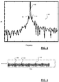
- FIGS. 3 and 4 depict waveforms exemplary of a capacitive discharge from a plasma chamber operated at a relatively low bias frequency f b and a relatively high source frequency f s for a RF power delivery system not applying the frequency offset techniques described herein.
- Waveform 90 of FIG. 3 shows the IMD, with waveform 90 having a peak 92 at f s and peaks 94, 96 indicating the IMD at f s - f b and f s + f b respectively.
- the IMD shown at peaks 94, 96 indicates areas of impedance fluctuation, which is undesirable.
- FIG. 4 depicts the modulating plasma current (in amperes) versus time. As can be seen in FIG.
- the peaks 100 indicate fluctuation in the plasma current resulting from corresponding impedance fluctuations.
- the peaks 100 are 1/ f b apart, which corresponds to a frequency of f b , the frequency of the bias RF signal.
- FIGS. 3 and 4 indicate that IMD introduced by the bias RF output signal, as evidenced by the resulting current fluctuations, introduces unwanted peaks in the plasma current. The impedance fluctuations hinder the desirable control of the RF system.
- FIGS. 5 and 6 demonstrate the effect of the impedance fluctuations introduced by RF power delivery systems not applying the frequency offset techniques described herein and the delivery of power to the load or a plasma chamber.
- a source RF power supply is operated at a relatively high frequency f s
- the bias power supply is operated at a relatively low frequency f b .
- the bias RF power supply thus, has a cycle time of 1/ f b .
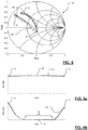
- FIG. 5 depicts the Smith chart 110 indicating the impedance fluctuations as the bias RF power supply applies the f b RF signal to a plasma chamber.
- Plot 116 in Smith chart 110 indicates the impedance fluctuates from a desirable position near the center of Smith chart 110 to an undesirable position near the outer boundaries of Smith chart 110. Near the outer boundaries of Smith chart 110, impedance is higher, increasing the reflected power, thereby reducing the power the source RF generator can deliver to the plasma chamber.
- FIGS. 6a and 6b indicate the variation in the respective forward power P FWD and reverse power P REV of the source RF signal applied to the plasma chamber as the impedance in the plasma chamber varies over a single period of the f b bias signal.
- the timescale for the forward power and reverse power in FIGS. 6a and 6b covers a 1/ f b period.
- Waveform 112 of FIG. 6a represents the forward power of the source RF signal and remains generally constant at or near an approximate maximum.
- Waveform 114 of FIG. 6b represents the reverse power of the source RF signal and fluctuates from at or near an approximate high, ramping down to approximately zero and remaining near zero until for a time D. Following the time D, the reverse power ramps upward to at or near an approximate high.
- dotted line 118 provides a reference of plot 116 of Smith chart 110 with the timescale of FIG. 6 .
- the reverse power shown in FIG. 6b is at or near an approximate maximum.
- the reverse power shown in FIG. 6b is also at or near an approximate maximum.
- the instances of generally high reverse power indicate a poor impedance match at the plasma chamber and coincide with points on plot 116 being located toward the outer boundaries of Smith chart 110.
- the reverse power shown in FIG. 6b is near zero. The region of reverse power being approximately zero coincides to the portion of plot 116 being near or below the imaginary axis of Smith chart 110.
- the impedance fluctuation described in connection with FIGS. 5 and 6 repeats for each cycle of the bias RF power signal, yielding generally high impedance fluctuations and corresponding high reverse power at the source RF power supply.
- the impedance fluctuations significantly impact the application of the source RF power signal for approximately 40% of the bias RF signal.
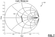
- FIGS. 7 and 8 demonstrate the improvement to the impedance fluctuations provided the system of the present disclosure to the impedance fluctuations over conventional RF power delivery systems.
- FIG. 7 depicts Smith chart 120 showing a plot 122. As can be seen from plot 122, impedance fluctuation is significantly reduced over the impedance plot 116 of Smith chart 110 in FIG. 5 .
- FIG. 8 depicts another example of a benefit provided by the present disclosure.
- FIG. 8 depicts waveforms of a bias RF power signal 124, a composite of the source RF power signal and the bias RF power signal 126, and a frequency offset signal 128.
- the frequency offset signal 128 applies only a single offset frequency over a portion of the bias waveform, and the single offset frequency is synchronized to a minimum of the composite of the source RF power signal and the bias RF power signal 126.
- Waveform 130 indicates reflected power when the system of the present disclosure is used to apply and offset frequency to the source RF signal.
- Waveform 132 of FIG. 9 indicates the reflected power for a system implemented without adding offset frequencies to the source RF power signal as described according to the present disclosure. As can be seen, waveform 130 indicates a significant decrease in reflected power over waveform 132.
- FIG. 10 depicts a waveform 126'.
- Waveform 126' depicts a portion of waveform 126 of FIG. 8 .
- Waveform 126' of FIG. 10 is intended to show the composite nature of waveform 126 of FIG. 8 .
- waveform 126 is a composite of the source RF power signal and the bias RF power signal.
- waveform 126 has a relatively low frequency component, provided by one of the source or the bias RF power supplies, and a relatively high frequency component, provided by the other of the source or the RF bias RF power supplies.
- Waveforms 126, 126' represent the RF signal sampled at an electrode of the plasma chamber, such as may be connected to source RF power supply.
- Composite waveform 126 thus includes a lower frequency component and a higher frequency component. In waveform 126', the gradual arc corresponds to the lower frequency signal, and the repeating sinusoidal peaks correspond to the higher frequency signal.
- Spatial and functional relationships between elements are described using various terms, including “connected,” “engaged,” “coupled,” “adjacent,” “next to,” “on top of,” “above,” “below,” and “disposed.” Unless explicitly described as being “direct,” when a relationship between first and second elements is described in the above disclosure, that relationship can be a direct relationship where no other intervening elements are present between the first and second elements, but can also be an indirect relationship where one or more intervening elements are present (either spatially or functionally) between the first and second elements.
- the phrase at least one of A, B, and C should be construed to mean a logical (A OR B OR C), using a non-exclusive logical OR, and should not be construed to mean "at least one of A, at least one of B, and at least one of C.”
- the term 'module' or the term 'controller' may be replaced with the term 'circuit.
- the term 'module' may refer to, be part of, or include: an Application Specific Integrated Circuit (ASIC); a digital, analog, or mixed analog/digital discrete circuit; a digital, analog, or mixed analog/digital integrated circuit; a combinational logic circuit; a field programmable gate array (FPGA); a processor circuit (shared, dedicated, or group) that executes code; a memory circuit (shared, dedicated, or group) that stores code executed by the processor circuit; other suitable hardware components that provide the described functionality; or a combination of some or all of the above, such as in a system-on-chip.
- ASIC Application Specific Integrated Circuit
- FPGA field programmable gate array
- the module may include one or more interface circuits.
- the interface circuits may include wired or wireless interfaces that are connected to a local area network (LAN), the Internet, a wide area network (WAN), or combinations thereof.
- LAN local area network
- WAN wide area network
- the functionality of any given module of the present disclosure may be distributed among multiple modules that are connected via interface circuits. For example, multiple modules may allow load balancing.
- a server (also known as remote, or cloud) module may accomplish some functionality on behalf of a client module.
- code may include software, firmware, and/or microcode, and may refer to programs, routines, functions, classes, data structures, and/or objects.
- shared processor circuit encompasses a single processor circuit that executes some or all code from multiple modules.
- group processor circuit encompasses a processor circuit that, in combination with additional processor circuits, executes some or all code from one or more modules. References to multiple processor circuits encompass multiple processor circuits on discrete dies, multiple processor circuits on a single die, multiple cores of a single processor circuit, multiple threads of a single processor circuit, or a combination of the above.
- shared memory circuit encompasses a single memory circuit that stores some or all code from multiple modules.
- group memory circuit encompasses a memory circuit that, in combination with additional memories, stores some or all code from one or more modules.
- the term memory circuit is a subset of the term computer-readable medium.
- the term computer-readable medium does not encompass transitory electrical or electromagnetic signals propagating through a medium (such as on a carrier wave); the term computer-readable medium may therefore be considered tangible and non-transitory.
- Non-limiting examples of a non-transitory, tangible computer-readable medium are nonvolatile memory circuits (such as a flash memory circuit, an erasable programmable read-only memory circuit, or a mask read-only memory circuit), volatile memory circuits (such as a static random access memory circuit or a dynamic random access memory circuit), magnetic storage media (such as an analog or digital magnetic tape or a hard disk drive), and optical storage media (such as a CD, a DVD, or a Blu-ray Disc).
- nonvolatile memory circuits such as a flash memory circuit, an erasable programmable read-only memory circuit, or a mask read-only memory circuit
- volatile memory circuits such as a static random access memory circuit or a dynamic random access memory circuit
- magnetic storage media such as an analog or digital magnetic tape or a hard disk drive
- optical storage media such as a CD, a DVD, or a Blu-ray Disc
- the apparatuses and methods described in this application may be partially or fully implemented by a special purpose computer created by configuring a general purpose computer to execute one or more particular functions embodied in computer programs.
- the functional blocks and flowchart elements described above serve as software specifications, which can be translated into the computer programs by the routine work of a skilled technician or programmer.
- the computer programs include processor-executable instructions that are stored on at least one non-transitory, tangible computer-readable medium.
- the computer programs may also include or rely on stored data.
- the computer programs may encompass a basic input/output system (BIOS) that interacts with hardware of the special purpose computer, device drivers that interact with particular devices of the special purpose computer, one or more operating systems, user applications, background services, background applications, etc.
- BIOS basic input/output system
- the computer programs may include: (i) descriptive text to be parsed, such as HTML (hypertext markup language) or XML (extensible markup language), (ii) assembly code, (iii) object code generated from source code by a compiler, (iv) source code for execution by an interpreter, (v) source code for compilation and execution by a just-in-time compiler, etc.
- source code may be written using syntax from languages including C, C++, C#, MATLAB®, Simulink®, Objective C, Haskell, Go, SQL, R, Lisp, Java®, Fortran, Perl, Pascal, Curl, OCaml, Javascript®, HTML5, Ada, ASP (active server pages), PHP, Scala, Eiffel, Smalltalk, Erlang, Ruby, Flash®, Visual Basic®, Lua, and Python®.
Landscapes
- Physics & Mathematics (AREA)
- Engineering & Computer Science (AREA)
- Plasma & Fusion (AREA)
- Chemical & Material Sciences (AREA)
- Analytical Chemistry (AREA)
- Plasma Technology (AREA)
- Drying Of Semiconductors (AREA)
Claims (14)
- Radiofrequenz-(RF)-Generator (12a), der Folgendes umfasst:eine RF-Leistungsquelle (14a); undeinen RF-Leistungsregler (20a), der mit der RF-Leistungsquelle gekoppelt ist, wobei der RF-Leistungsregler zum Erzeugen eines Steuersignals (28a) konfiguriert ist, um einen RF-Ausgang (22a) von der RF-Leistungsquelle (14a) zu variieren, wobei der RF-Leistungsregler (20a) zum Arbeiten als Reaktion auf ein Triggersignal (30) konfiguriert ist, dadurch gekennzeichnet, dass der RF-Leistungsregler zum Einführen eines Frequenzversatzes in den RF-Ausgang (22a) konfiguriert ist,wobei der Frequenzversatz gemäß einem externen RF-Ausgang von einem externen RF-Generator (12b) variiert.
- RF-Generator (12a) nach Anspruch 1, wobei der RF-Ausgang (22a) ein RF-Quellsignal (f1) ist, das an eine Plasmakammer (32) angelegt wird, und der externe RF-Ausgang (22b) ein RF-Vorspannungssignal (f2) ist, das an die Plasmakammer (32) angelegt wird.
- RF-Generator (12a) nach einem der vorherigen Ansprüche, wobei der RF-Leistungsregler (20a) zum Einführen des Frequenzversatzes in den RF-Ausgang (22a) gemäß einem Timing konfiguriert ist, das gemäß dem Triggersignal variiert, wobei das Triggersignal eine relative Position des externen RF-Ausgangs (22b) anzeigt.
- RF-Generator (12a) nach einem der vorherigen Ansprüche, wobei der Frequenzversatz mehrere Frequenzen beinhaltet, die der RF-Leistungsregler (20a) in einer/m vorbestimmten Reihenfolge und Timing gemäß dem Triggersignal in den RF-Ausgang (22a) einzuführen konfiguriert ist.
- RF-Generator (12a) nach einem der vorherigen Ansprüche, wobei der RF-Leistungsregler (20a) zum Aktualisieren des Frequenzversatzes gemäß dem externen RF-Ausgang (22b) konfiguriert ist.
- RF-Generator (12a) nach einem der vorherigen Ansprüche, wobei der Frequenzversatz gemäß einer durch den externen RF-Ausgang (22b) verursachten Intermodulationsverzerrung variiert.
- RF-Generator (12a) nach einem der vorherigen Ansprüche, wobei der RF-Leistungsregler (20a) ferner ein Wiedergabemodul (34) umfasst, wobei das Wiedergabemodul zum Erkennen des Triggersignals konfiguriert ist, wobei das Wiedergabemodul zum Einleiten der Einführung eines Frequenzversatzes in den RF-Ausgang konfiguriert ist.
- RF-Generator (12a) nach einem der vorherigen Ansprüche, wobei der RF-Leistungsregler (20a) ferner eine Nachschlagtabelle umfasst, wobei die Nachschlagtabelle zum Speichern des durch das Wiedergabemodul (34) eingeführten Frequenzversatzes konfiguriert ist.
- RF-Generator (12a) nach einem der vorherigen Ansprüche, wobei der RF-Leistungsregler (20a) ferner ein Aktualisierungsmodul (38) umfasst, wobei das Aktualisierungsmodul zum Aktualisieren des Frequenzversatzes gemäß einem elektrischen Kennwert des RF-Ausgangs (22a) konfiguriert ist.
- RF-Generator (12a) nach einem der vorherigen Ansprüche, wobei das Triggersignal eines aus periodisch, nicht-periodisch, synchron zu einem vorbestimmten Ereignis oder asynchron ist.
- Verfahren zum Erzeugen eines Radiofrequenz-(RF)-Signals, das Folgendes beinhaltet:Koppeln eines Leistungsreglers (20a) mit einer RF-Leistungsquelle (14a);Steuern eines ersten RF-Generators (12a) zum Ausgeben eines ersten RF-Ausgangssignals (f1);Erzeugen eines Steuersignals, wobei das Steuersignal einen elektrischen Kennwert des ersten RF-Ausgangssignals variiert; gekennzeichnet durchVariieren des Steuersignals, um einen Frequenzversatz in das erste RF-Ausgangssignal einzuführen, wobei der Frequenzversatz gemäß einem von einem externen RF-Generator empfangenen zweiten RF-Ausgangssignal variiert.
- Verfahren nach Anspruch 11, das ferner das Einführen des Frequenzversatzes in das erste RF-Ausgangssignal (f1) gemäß einem Triggersignal beinhaltet, wobei das Triggersignal gemäß dem zweiten RF-Ausgangssignal (f2) oder einer Impedanzschwankung in einer das erste RF-Ausgangssignal (f1) empfangenden Last (32) variiert.
- Verfahren nach Anspruch 11 oder 12, das ferner das Einkoppeln des ersten RF-Ausgangssignals (f1) in eine Quellelektrode einer Plasmakammer (32) und das Einkoppeln des anliegenden zweiten RF-Ausgangssignals (f2) in eine Bias-Elektrode einer Plasmakammer (32) beinhaltet.
- Verfahren nach einem der Ansprüche 11 bis 13, das ferner das Aktualisieren des Frequenzversatzes gemäß dem Ausgang des zweiten RF-Ausgangssignals (f2) oder einer Impedanzschwankung in einer mit dem ersten RF-Generator (12a) gekoppelten Last (32) beinhaltet.
Priority Applications (1)
| Application Number | Priority Date | Filing Date | Title |
|---|---|---|---|
| EP21151450.0A EP3840013B1 (de) | 2015-09-01 | 2016-08-29 | System zur unterdrückung der plasma-hf-verzerrung |
Applications Claiming Priority (3)
| Application Number | Priority Date | Filing Date | Title |
|---|---|---|---|
| US201562212661P | 2015-09-01 | 2015-09-01 | |
| US15/236,661 US9947514B2 (en) | 2015-09-01 | 2016-08-15 | Plasma RF bias cancellation system |
| PCT/US2016/049293 WO2017040415A1 (en) | 2015-09-01 | 2016-08-29 | Plasma rf bias cancellation system |
Related Child Applications (2)
| Application Number | Title | Priority Date | Filing Date |
|---|---|---|---|
| EP21151450.0A Division EP3840013B1 (de) | 2015-09-01 | 2016-08-29 | System zur unterdrückung der plasma-hf-verzerrung |
| EP21151450.0A Division-Into EP3840013B1 (de) | 2015-09-01 | 2016-08-29 | System zur unterdrückung der plasma-hf-verzerrung |
Publications (3)
| Publication Number | Publication Date |
|---|---|
| EP3345207A1 EP3345207A1 (de) | 2018-07-11 |
| EP3345207A4 EP3345207A4 (de) | 2019-04-10 |
| EP3345207B1 true EP3345207B1 (de) | 2021-02-24 |
Family
ID=58096629
Family Applications (2)
| Application Number | Title | Priority Date | Filing Date |
|---|---|---|---|
| EP21151450.0A Active EP3840013B1 (de) | 2015-09-01 | 2016-08-29 | System zur unterdrückung der plasma-hf-verzerrung |
| EP16842760.7A Active EP3345207B1 (de) | 2015-09-01 | 2016-08-29 | Plasma-hf-vorspannungsunterdrückungssystem |
Family Applications Before (1)
| Application Number | Title | Priority Date | Filing Date |
|---|---|---|---|
| EP21151450.0A Active EP3840013B1 (de) | 2015-09-01 | 2016-08-29 | System zur unterdrückung der plasma-hf-verzerrung |
Country Status (7)
| Country | Link |
|---|---|
| US (1) | US9947514B2 (de) |
| EP (2) | EP3840013B1 (de) |
| JP (2) | JP6785862B2 (de) |
| KR (1) | KR102381837B1 (de) |
| CN (1) | CN108140530B (de) |
| TW (1) | TWI673756B (de) |
| WO (1) | WO2017040415A1 (de) |
Families Citing this family (61)
| Publication number | Priority date | Publication date | Assignee | Title |
|---|---|---|---|---|
| US10049857B2 (en) | 2014-12-04 | 2018-08-14 | Mks Instruments, Inc. | Adaptive periodic waveform controller |
| US9947514B2 (en) | 2015-09-01 | 2018-04-17 | Mks Instruments, Inc. | Plasma RF bias cancellation system |
| US10546724B2 (en) * | 2017-05-10 | 2020-01-28 | Mks Instruments, Inc. | Pulsed, bidirectional radio frequency source/load |
| US11651939B2 (en) * | 2017-07-07 | 2023-05-16 | Advanced Energy Industries, Inc. | Inter-period control system for plasma power delivery system and method of operating same |
| US11615943B2 (en) * | 2017-07-07 | 2023-03-28 | Advanced Energy Industries, Inc. | Inter-period control for passive power distribution of multiple electrode inductive plasma source |
| CN115662868A (zh) * | 2017-07-07 | 2023-01-31 | 先进能源工业公司 | 等离子体功率输送系统的周期间控制系统及其操作方法 |
| JP7209483B2 (ja) * | 2017-10-10 | 2023-01-20 | 東京エレクトロン株式会社 | プラズマ処理装置および測定回路 |
| KR102439221B1 (ko) * | 2017-12-14 | 2022-09-01 | 프로디자인 소닉스, 인크. | 음향 트랜스듀서 구동기 및 제어기 |
| JP7175239B2 (ja) * | 2018-06-22 | 2022-11-18 | 東京エレクトロン株式会社 | 制御方法、プラズマ処理装置、プログラム及び記憶媒体 |
| JP6846387B2 (ja) * | 2018-06-22 | 2021-03-24 | 東京エレクトロン株式会社 | プラズマ処理方法及びプラズマ処理装置 |
| US10504744B1 (en) * | 2018-07-19 | 2019-12-10 | Lam Research Corporation | Three or more states for achieving high aspect ratio dielectric etch |
| WO2020068107A1 (en) * | 2018-09-28 | 2020-04-02 | Lam Research Corporation | Systems and methods for optimizing power delivery to an electrode of a plasma chamber |
| JP7122268B2 (ja) * | 2019-02-05 | 2022-08-19 | 東京エレクトロン株式会社 | プラズマ処理装置 |
| US11476092B2 (en) * | 2019-05-31 | 2022-10-18 | Mks Instruments, Inc. | System and method of power generation with phase linked solid-state generator modules |
| US11177115B2 (en) * | 2019-06-03 | 2021-11-16 | Applied Materials, Inc. | Dual-level pulse tuning |
| CN114207768B (zh) * | 2019-06-07 | 2024-08-20 | 朗姆研究公司 | 用于在kHz RF发生器的操作循环内调谐MHz RF发生器的系统和方法 |
| US11158488B2 (en) * | 2019-06-26 | 2021-10-26 | Mks Instruments, Inc. | High speed synchronization of plasma source/bias power delivery |
| US11315757B2 (en) | 2019-08-13 | 2022-04-26 | Mks Instruments, Inc. | Method and apparatus to enhance sheath formation, evolution and pulse to pulse stability in RF powered plasma applications |
| EP3792955B1 (de) | 2019-09-10 | 2021-10-27 | Comet AG | Hf-leistungsgenerator mit analogen und digitalen detektoren |
| US10741363B1 (en) * | 2019-10-08 | 2020-08-11 | Mks Instruments, Inc. | Extremum seeking control apparatus and method for automatic frequency tuning for RF impedance matching |
| US11232931B2 (en) | 2019-10-21 | 2022-01-25 | Mks Instruments, Inc. | Intermodulation distortion mitigation using electronic variable capacitor |
| JP7437142B2 (ja) * | 2019-11-25 | 2024-02-22 | 株式会社ダイヘン | 高周波電源システム |
| WO2021113387A1 (en) | 2019-12-02 | 2021-06-10 | Lam Research Corporation | Impedance transformation in radio-frequency-assisted plasma generation |
| US12266505B2 (en) * | 2020-02-27 | 2025-04-01 | Lam Research Corporation | Systems and methods for using binning to increase power during a low frequency cycle |
| JP7450435B2 (ja) * | 2020-03-30 | 2024-03-15 | 株式会社ダイヘン | 高周波電源システム |
| US11276601B2 (en) | 2020-04-10 | 2022-03-15 | Applied Materials, Inc. | Apparatus and methods for manipulating power at an edge ring in a plasma processing device |
| KR20230021739A (ko) | 2020-06-12 | 2023-02-14 | 램 리써치 코포레이션 | Rf 커플링 구조체들에 의한 플라즈마 형성의 제어 |
| KR20230034970A (ko) | 2020-07-08 | 2023-03-10 | 램 리써치 코포레이션 | 플라즈마 프로세싱 시스템의 무선 주파수 (radiofrequency) 공급 시스템으로부터 프로세스 제어 정보를 추출하기 위한 시스템들 및 방법들 |
| US11527384B2 (en) * | 2020-11-24 | 2022-12-13 | Mks Instruments, Inc. | Apparatus and tuning method for mitigating RF load impedance variations due to periodic disturbances |
| JP7544594B2 (ja) | 2020-12-25 | 2024-09-03 | 株式会社ダイヘン | 高周波電源システム |
| WO2022159596A1 (en) * | 2021-01-20 | 2022-07-28 | Advanced Energy Industries, Inc. | Power delivery to a plasma via inductive coupling |
| WO2022163535A1 (ja) * | 2021-01-29 | 2022-08-04 | 東京エレクトロン株式会社 | プラズマ処理装置及びソース高周波電力のソース周波数を制御する方法 |
| KR102786710B1 (ko) * | 2021-01-29 | 2025-03-25 | 도쿄엘렉트론가부시키가이샤 | 플라즈마 처리 장치 및 소스 고주파 전력의 소스 주파수를 제어하는 방법 |
| JP7511501B2 (ja) * | 2021-02-10 | 2024-07-05 | 東京エレクトロン株式会社 | プラズマ処理装置及び監視装置 |
| WO2022211915A1 (en) * | 2021-04-01 | 2022-10-06 | Advanced Energy Industries, Inc. | Inter-period control system for plasma power delivery system and method of operating the same |
| WO2022216419A1 (en) * | 2021-04-07 | 2022-10-13 | Lam Research Corporation | Systems and methods for controlling a plasma sheath characteristic |
| JP7434669B2 (ja) * | 2021-06-21 | 2024-02-20 | 東京エレクトロン株式会社 | プラズマ処理装置及びプラズマ処理方法 |
| JP7633133B2 (ja) | 2021-09-30 | 2025-02-19 | 株式会社ダイヘン | 高周波電源装置 |
| TW202336804A (zh) * | 2021-11-19 | 2023-09-16 | 日商東京威力科創股份有限公司 | 電漿處理裝置、電源系統、控制方法、程式及記憶媒體 |
| TW202341227A (zh) * | 2021-12-27 | 2023-10-16 | 日商東京威力科創股份有限公司 | 電漿處理裝置、電源系統、控制方法、程式及記憶媒體 |
| JP2023098297A (ja) * | 2021-12-28 | 2023-07-10 | 株式会社ダイヘン | 高周波電源装置 |
| JP7695880B2 (ja) | 2021-12-28 | 2025-06-19 | 株式会社ダイヘン | 高周波電源装置 |
| JP2023097863A (ja) | 2021-12-28 | 2023-07-10 | 株式会社ダイヘン | 高周波電源システム |
| JP7763099B2 (ja) * | 2021-12-28 | 2025-10-31 | 株式会社ダイヘン | 高周波電源装置 |
| JP2023098203A (ja) | 2021-12-28 | 2023-07-10 | 株式会社ダイヘン | 高周波電源装置 |
| US12131884B2 (en) | 2022-01-12 | 2024-10-29 | Mks Instruments, Inc. | Pulse and bias synchronization methods and systems |
| JP2025508379A (ja) * | 2022-02-18 | 2025-03-26 | ラム リサーチ コーポレーション | 中心周波数同調のためのシステムおよび方法 |
| CN115209605B (zh) * | 2022-06-20 | 2025-04-08 | 中国科学院合肥物质科学研究院 | 一种微波等离子体照明系统及其自动控制方法 |
| US20240055228A1 (en) * | 2022-08-10 | 2024-02-15 | Mks Instruments, Inc. | Plasma Process Control of Multi-Electrode Systems Equipped with Ion Energy Sensors |
| DE102022122044A1 (de) * | 2022-08-31 | 2024-02-29 | TRUMPF Hüttinger GmbH + Co. KG | Plasmazustandsüberwachungsvorrichtung zum Anschluss an eine Impedanzanpassungsschaltung für ein Plasmaerzeugungssystem, ein Plasmaerzeugungssystem und ein Verfahren zur Überwachung des Plasmaerzeugungssystems |
| US11996269B2 (en) | 2022-09-08 | 2024-05-28 | Mks Instruments, Inc. | Extremum seeking control apparatuses with online parameter adjustment and methods |
| CN115765652A (zh) * | 2022-11-23 | 2023-03-07 | 成都四威功率电子科技有限公司 | 一种用于宽带微波信号混合的功放架构及其工作方法 |
| TW202442033A (zh) * | 2022-11-30 | 2024-10-16 | 日商東京威力科創股份有限公司 | 電漿處理裝置、電源系統及頻率控制方法 |
| JP2024095371A (ja) | 2022-12-28 | 2024-07-10 | 株式会社ダイヘン | 高周波電力供給システム |
| JP2024095372A (ja) | 2022-12-28 | 2024-07-10 | 株式会社ダイヘン | 高周波電力供給システムの制御方法 |
| JP2024095370A (ja) | 2022-12-28 | 2024-07-10 | 株式会社ダイヘン | 高周波電力供給システム |
| JP2024094788A (ja) | 2022-12-28 | 2024-07-10 | 株式会社ダイヘン | 高周波電源装置 |
| JP2024095373A (ja) | 2022-12-28 | 2024-07-10 | 株式会社ダイヘン | 高周波電力供給システム |
| US12278090B2 (en) * | 2023-04-18 | 2025-04-15 | Mks Instruments, Inc. | Enhanced tuning methods for mitigating RF load impedance variations due to periodic disturbances |
| KR102884960B1 (ko) * | 2024-01-22 | 2025-11-13 | (주)아센디아 | Rf 제너레이터 |
| JP2026006642A (ja) | 2024-06-28 | 2026-01-16 | 株式会社ダイヘン | 高周波電力供給システムの制御方法 |
Family Cites Families (32)
| Publication number | Priority date | Publication date | Assignee | Title |
|---|---|---|---|---|
| US6174450B1 (en) * | 1997-04-16 | 2001-01-16 | Lam Research Corporation | Methods and apparatus for controlling ion energy and plasma density in a plasma processing system |
| US6875366B2 (en) * | 2000-09-12 | 2005-04-05 | Hitachi, Ltd. | Plasma processing apparatus and method with controlled biasing functions |
| WO2003029513A1 (en) * | 2001-09-28 | 2003-04-10 | Tokyo Electron Limited | Hybrid plasma processing apparatus |
| US6707255B2 (en) | 2002-07-10 | 2004-03-16 | Eni Technology, Inc. | Multirate processing for metrology of plasma RF source |
| US7247218B2 (en) * | 2003-05-16 | 2007-07-24 | Applied Materials, Inc. | Plasma density, energy and etch rate measurements at bias power input and real time feedback control of plasma source and bias power |
| US7602127B2 (en) * | 2005-04-18 | 2009-10-13 | Mks Instruments, Inc. | Phase and frequency control of a radio frequency generator from an external source |
| JP4879548B2 (ja) | 2005-09-30 | 2012-02-22 | 株式会社ダイヘン | 高周波電源装置 |
| US7727413B2 (en) | 2006-04-24 | 2010-06-01 | Applied Materials, Inc. | Dual plasma source process using a variable frequency capacitively coupled source to control plasma ion density |
| US7902991B2 (en) * | 2006-09-21 | 2011-03-08 | Applied Materials, Inc. | Frequency monitoring to detect plasma process abnormality |
| JP5426811B2 (ja) * | 2006-11-22 | 2014-02-26 | パール工業株式会社 | 高周波電源装置 |
| JP4905304B2 (ja) * | 2007-09-10 | 2012-03-28 | 東京エレクトロン株式会社 | プラズマ処理装置、プラズマ処理方法及び記憶媒体 |
| US9856558B2 (en) * | 2008-03-14 | 2018-01-02 | Applied Materials, Inc. | Physical vapor deposition method with a source of isotropic ion velocity distribution at the wafer surface |
| KR101528528B1 (ko) * | 2008-05-14 | 2015-06-12 | 어플라이드 머티어리얼스, 인코포레이티드 | Rf 전력 전달을 위한 시간 분해된 조정 방식을 이용하는 펄스화된 플라즈마 처리를 위한 방법 및 장치 |
| US7967944B2 (en) * | 2008-05-29 | 2011-06-28 | Applied Materials, Inc. | Method of plasma load impedance tuning by modulation of an unmatched low power RF generator |
| US8357264B2 (en) * | 2008-05-29 | 2013-01-22 | Applied Materials, Inc. | Plasma reactor with plasma load impedance tuning for engineered transients by synchronized modulation of a source power or bias power RF generator |
| US9378930B2 (en) * | 2009-03-05 | 2016-06-28 | Applied Materials, Inc. | Inductively coupled plasma reactor having RF phase control and methods of use thereof |
| CN101989525A (zh) * | 2009-08-05 | 2011-03-23 | 中微半导体设备(上海)有限公司 | 具备可切换偏置频率的等离子体处理腔及可切换匹配网络 |
| US8491759B2 (en) * | 2010-10-20 | 2013-07-23 | COMET Technologies USA, Inc. | RF impedance matching network with secondary frequency and sub-harmonic variant |
| JP5367000B2 (ja) * | 2011-03-24 | 2013-12-11 | 東京エレクトロン株式会社 | プラズマ処理装置 |
| US8952765B2 (en) * | 2012-03-23 | 2015-02-10 | Mks Instruments, Inc. | System and methods of bimodal automatic power and frequency tuning of RF generators |
| TWI599272B (zh) * | 2012-09-14 | 2017-09-11 | 蘭姆研究公司 | 根據三個或更多狀態之功率及頻率調整 |
| US9408288B2 (en) * | 2012-09-14 | 2016-08-02 | Lam Research Corporation | Edge ramping |
| US9082589B2 (en) * | 2012-10-09 | 2015-07-14 | Novellus Systems, Inc. | Hybrid impedance matching for inductively coupled plasma system |
| CN103730316B (zh) | 2012-10-16 | 2016-04-06 | 中微半导体设备(上海)有限公司 | 一种等离子处理方法及等离子处理装置 |
| US9593410B2 (en) * | 2013-03-05 | 2017-03-14 | Applied Materials, Inc. | Methods and apparatus for stable substrate processing with multiple RF power supplies |
| US10821542B2 (en) | 2013-03-15 | 2020-11-03 | Mks Instruments, Inc. | Pulse synchronization by monitoring power in another frequency band |
| US9336995B2 (en) * | 2013-04-26 | 2016-05-10 | Mks Instruments, Inc. | Multiple radio frequency power supply control of frequency and phase |
| US10469108B2 (en) | 2013-05-09 | 2019-11-05 | Lam Research Corporation | Systems and methods for using computer-generated models to reduce reflected power towards a high frequency RF generator during a cycle of operations of a low frequency RF generator |
| US10276350B2 (en) | 2013-05-09 | 2019-04-30 | Lam Research Corporation | Systems and methods for using computer-generated models to reduce reflected power towards an RF generator during state transitions of the RF generator by controlling RF values of the RF generator |
| US9711332B2 (en) | 2013-05-09 | 2017-07-18 | Lam Research Corporation | Systems and methods for tuning an impedance matching network in a step-wise fashion for multiple states of an RF generator |
| US9536749B2 (en) | 2014-12-15 | 2017-01-03 | Lam Research Corporation | Ion energy control by RF pulse shape |
| US9947514B2 (en) | 2015-09-01 | 2018-04-17 | Mks Instruments, Inc. | Plasma RF bias cancellation system |
-
2016
- 2016-08-15 US US15/236,661 patent/US9947514B2/en active Active
- 2016-08-29 WO PCT/US2016/049293 patent/WO2017040415A1/en not_active Ceased
- 2016-08-29 CN CN201680050640.0A patent/CN108140530B/zh active Active
- 2016-08-29 JP JP2018530648A patent/JP6785862B2/ja active Active
- 2016-08-29 KR KR1020187009295A patent/KR102381837B1/ko active Active
- 2016-08-29 EP EP21151450.0A patent/EP3840013B1/de active Active
- 2016-08-29 EP EP16842760.7A patent/EP3345207B1/de active Active
- 2016-09-01 TW TW105128291A patent/TWI673756B/zh active
-
2020
- 2020-04-27 JP JP2020078296A patent/JP6935537B2/ja active Active
Non-Patent Citations (1)
| Title |
|---|
| None * |
Also Published As
| Publication number | Publication date |
|---|---|
| KR102381837B1 (ko) | 2022-04-04 |
| CN108140530A (zh) | 2018-06-08 |
| EP3345207A4 (de) | 2019-04-10 |
| EP3840013B1 (de) | 2023-11-08 |
| WO2017040415A1 (en) | 2017-03-09 |
| EP3840013A1 (de) | 2021-06-23 |
| EP3345207A1 (de) | 2018-07-11 |
| JP2018536295A (ja) | 2018-12-06 |
| KR20180038059A (ko) | 2018-04-13 |
| US9947514B2 (en) | 2018-04-17 |
| TWI673756B (zh) | 2019-10-01 |
| JP6935537B2 (ja) | 2021-09-15 |
| CN108140530B (zh) | 2021-06-22 |
| JP2020129549A (ja) | 2020-08-27 |
| JP6785862B2 (ja) | 2020-11-18 |
| US20170062187A1 (en) | 2017-03-02 |
| TW201719711A (zh) | 2017-06-01 |
Similar Documents
| Publication | Publication Date | Title |
|---|---|---|
| EP3345207B1 (de) | Plasma-hf-vorspannungsunterdrückungssystem | |
| US11935726B2 (en) | High speed synchronization of plasma source/bias power delivery | |
| TWI697205B (zh) | 射頻電漿系統中用來控制阻礙及imd堵塞損害的自動調整反制之射頻產生器、裝置及方法 | |
| US10666206B2 (en) | Supervisory control of radio frequency (RF) impedance tuning operation | |
| US12183549B2 (en) | Apparatus and tuning method for mitigating RF load impedance variations due to periodic disturbances | |
| WO2025116995A1 (en) | Source tuning with pulsed dc bias | |
| EP4416754A1 (de) | Impedanzanpassung in einem hf-stromerzeugungssystem | |
| WO2024158548A1 (en) | Non-invasive ied estimation for pulsed-dc and low frequency applications |
Legal Events
| Date | Code | Title | Description |
|---|---|---|---|
| STAA | Information on the status of an ep patent application or granted ep patent |
Free format text: STATUS: THE INTERNATIONAL PUBLICATION HAS BEEN MADE |
|
| PUAI | Public reference made under article 153(3) epc to a published international application that has entered the european phase |
Free format text: ORIGINAL CODE: 0009012 |
|
| STAA | Information on the status of an ep patent application or granted ep patent |
Free format text: STATUS: REQUEST FOR EXAMINATION WAS MADE |
|
| 17P | Request for examination filed |
Effective date: 20180327 |
|
| AK | Designated contracting states |
Kind code of ref document: A1 Designated state(s): AL AT BE BG CH CY CZ DE DK EE ES FI FR GB GR HR HU IE IS IT LI LT LU LV MC MK MT NL NO PL PT RO RS SE SI SK SM TR |
|
| AX | Request for extension of the european patent |
Extension state: BA ME |
|
| DAV | Request for validation of the european patent (deleted) | ||
| DAX | Request for extension of the european patent (deleted) | ||
| A4 | Supplementary search report drawn up and despatched |
Effective date: 20190308 |
|
| RIC1 | Information provided on ipc code assigned before grant |
Ipc: H01J 37/32 20060101AFI20190304BHEP |
|
| GRAP | Despatch of communication of intention to grant a patent |
Free format text: ORIGINAL CODE: EPIDOSNIGR1 |
|
| STAA | Information on the status of an ep patent application or granted ep patent |
Free format text: STATUS: GRANT OF PATENT IS INTENDED |
|
| INTG | Intention to grant announced |
Effective date: 20200914 |
|
| GRAS | Grant fee paid |
Free format text: ORIGINAL CODE: EPIDOSNIGR3 |
|
| GRAA | (expected) grant |
Free format text: ORIGINAL CODE: 0009210 |
|
| STAA | Information on the status of an ep patent application or granted ep patent |
Free format text: STATUS: THE PATENT HAS BEEN GRANTED |
|
| AK | Designated contracting states |
Kind code of ref document: B1 Designated state(s): AL AT BE BG CH CY CZ DE DK EE ES FI FR GB GR HR HU IE IS IT LI LT LU LV MC MK MT NL NO PL PT RO RS SE SI SK SM TR |
|
| REG | Reference to a national code |
Ref country code: CH Ref legal event code: EP |
|
| REG | Reference to a national code |
Ref country code: DE Ref legal event code: R096 Ref document number: 602016053297 Country of ref document: DE |
|
| REG | Reference to a national code |
Ref country code: AT Ref legal event code: REF Ref document number: 1365544 Country of ref document: AT Kind code of ref document: T Effective date: 20210315 |
|
| REG | Reference to a national code |
Ref country code: IE Ref legal event code: FG4D |
|
| REG | Reference to a national code |
Ref country code: LT Ref legal event code: MG9D |
|
| REG | Reference to a national code |
Ref country code: NL Ref legal event code: MP Effective date: 20210224 |
|
| PG25 | Lapsed in a contracting state [announced via postgrant information from national office to epo] |
Ref country code: HR Free format text: LAPSE BECAUSE OF FAILURE TO SUBMIT A TRANSLATION OF THE DESCRIPTION OR TO PAY THE FEE WITHIN THE PRESCRIBED TIME-LIMIT Effective date: 20210224 Ref country code: FI Free format text: LAPSE BECAUSE OF FAILURE TO SUBMIT A TRANSLATION OF THE DESCRIPTION OR TO PAY THE FEE WITHIN THE PRESCRIBED TIME-LIMIT Effective date: 20210224 Ref country code: GR Free format text: LAPSE BECAUSE OF FAILURE TO SUBMIT A TRANSLATION OF THE DESCRIPTION OR TO PAY THE FEE WITHIN THE PRESCRIBED TIME-LIMIT Effective date: 20210525 Ref country code: PT Free format text: LAPSE BECAUSE OF FAILURE TO SUBMIT A TRANSLATION OF THE DESCRIPTION OR TO PAY THE FEE WITHIN THE PRESCRIBED TIME-LIMIT Effective date: 20210624 Ref country code: NO Free format text: LAPSE BECAUSE OF FAILURE TO SUBMIT A TRANSLATION OF THE DESCRIPTION OR TO PAY THE FEE WITHIN THE PRESCRIBED TIME-LIMIT Effective date: 20210524 Ref country code: BG Free format text: LAPSE BECAUSE OF FAILURE TO SUBMIT A TRANSLATION OF THE DESCRIPTION OR TO PAY THE FEE WITHIN THE PRESCRIBED TIME-LIMIT Effective date: 20210524 Ref country code: LT Free format text: LAPSE BECAUSE OF FAILURE TO SUBMIT A TRANSLATION OF THE DESCRIPTION OR TO PAY THE FEE WITHIN THE PRESCRIBED TIME-LIMIT Effective date: 20210224 |
|
| REG | Reference to a national code |
Ref country code: AT Ref legal event code: MK05 Ref document number: 1365544 Country of ref document: AT Kind code of ref document: T Effective date: 20210224 |
|
| PG25 | Lapsed in a contracting state [announced via postgrant information from national office to epo] |
Ref country code: SE Free format text: LAPSE BECAUSE OF FAILURE TO SUBMIT A TRANSLATION OF THE DESCRIPTION OR TO PAY THE FEE WITHIN THE PRESCRIBED TIME-LIMIT Effective date: 20210224 Ref country code: LV Free format text: LAPSE BECAUSE OF FAILURE TO SUBMIT A TRANSLATION OF THE DESCRIPTION OR TO PAY THE FEE WITHIN THE PRESCRIBED TIME-LIMIT Effective date: 20210224 Ref country code: PL Free format text: LAPSE BECAUSE OF FAILURE TO SUBMIT A TRANSLATION OF THE DESCRIPTION OR TO PAY THE FEE WITHIN THE PRESCRIBED TIME-LIMIT Effective date: 20210224 Ref country code: NL Free format text: LAPSE BECAUSE OF FAILURE TO SUBMIT A TRANSLATION OF THE DESCRIPTION OR TO PAY THE FEE WITHIN THE PRESCRIBED TIME-LIMIT Effective date: 20210224 Ref country code: RS Free format text: LAPSE BECAUSE OF FAILURE TO SUBMIT A TRANSLATION OF THE DESCRIPTION OR TO PAY THE FEE WITHIN THE PRESCRIBED TIME-LIMIT Effective date: 20210224 |
|
| PG25 | Lapsed in a contracting state [announced via postgrant information from national office to epo] |
Ref country code: IS Free format text: LAPSE BECAUSE OF FAILURE TO SUBMIT A TRANSLATION OF THE DESCRIPTION OR TO PAY THE FEE WITHIN THE PRESCRIBED TIME-LIMIT Effective date: 20210624 |
|
| PG25 | Lapsed in a contracting state [announced via postgrant information from national office to epo] |
Ref country code: EE Free format text: LAPSE BECAUSE OF FAILURE TO SUBMIT A TRANSLATION OF THE DESCRIPTION OR TO PAY THE FEE WITHIN THE PRESCRIBED TIME-LIMIT Effective date: 20210224 Ref country code: CZ Free format text: LAPSE BECAUSE OF FAILURE TO SUBMIT A TRANSLATION OF THE DESCRIPTION OR TO PAY THE FEE WITHIN THE PRESCRIBED TIME-LIMIT Effective date: 20210224 Ref country code: AT Free format text: LAPSE BECAUSE OF FAILURE TO SUBMIT A TRANSLATION OF THE DESCRIPTION OR TO PAY THE FEE WITHIN THE PRESCRIBED TIME-LIMIT Effective date: 20210224 Ref country code: SM Free format text: LAPSE BECAUSE OF FAILURE TO SUBMIT A TRANSLATION OF THE DESCRIPTION OR TO PAY THE FEE WITHIN THE PRESCRIBED TIME-LIMIT Effective date: 20210224 |
|
| REG | Reference to a national code |
Ref country code: DE Ref legal event code: R097 Ref document number: 602016053297 Country of ref document: DE |
|
| PG25 | Lapsed in a contracting state [announced via postgrant information from national office to epo] |
Ref country code: DK Free format text: LAPSE BECAUSE OF FAILURE TO SUBMIT A TRANSLATION OF THE DESCRIPTION OR TO PAY THE FEE WITHIN THE PRESCRIBED TIME-LIMIT Effective date: 20210224 Ref country code: RO Free format text: LAPSE BECAUSE OF FAILURE TO SUBMIT A TRANSLATION OF THE DESCRIPTION OR TO PAY THE FEE WITHIN THE PRESCRIBED TIME-LIMIT Effective date: 20210224 Ref country code: SK Free format text: LAPSE BECAUSE OF FAILURE TO SUBMIT A TRANSLATION OF THE DESCRIPTION OR TO PAY THE FEE WITHIN THE PRESCRIBED TIME-LIMIT Effective date: 20210224 |
|
| PLBE | No opposition filed within time limit |
Free format text: ORIGINAL CODE: 0009261 |
|
| STAA | Information on the status of an ep patent application or granted ep patent |
Free format text: STATUS: NO OPPOSITION FILED WITHIN TIME LIMIT |
|
| PG25 | Lapsed in a contracting state [announced via postgrant information from national office to epo] |
Ref country code: AL Free format text: LAPSE BECAUSE OF FAILURE TO SUBMIT A TRANSLATION OF THE DESCRIPTION OR TO PAY THE FEE WITHIN THE PRESCRIBED TIME-LIMIT Effective date: 20210224 Ref country code: ES Free format text: LAPSE BECAUSE OF FAILURE TO SUBMIT A TRANSLATION OF THE DESCRIPTION OR TO PAY THE FEE WITHIN THE PRESCRIBED TIME-LIMIT Effective date: 20210224 |
|
| 26N | No opposition filed |
Effective date: 20211125 |
|
| PG25 | Lapsed in a contracting state [announced via postgrant information from national office to epo] |
Ref country code: SI Free format text: LAPSE BECAUSE OF FAILURE TO SUBMIT A TRANSLATION OF THE DESCRIPTION OR TO PAY THE FEE WITHIN THE PRESCRIBED TIME-LIMIT Effective date: 20210224 |
|
| REG | Reference to a national code |
Ref country code: CH Ref legal event code: PL |
|
| PG25 | Lapsed in a contracting state [announced via postgrant information from national office to epo] |
Ref country code: MC Free format text: LAPSE BECAUSE OF FAILURE TO SUBMIT A TRANSLATION OF THE DESCRIPTION OR TO PAY THE FEE WITHIN THE PRESCRIBED TIME-LIMIT Effective date: 20210224 |
|
| REG | Reference to a national code |
Ref country code: BE Ref legal event code: MM Effective date: 20210831 |
|
| PG25 | Lapsed in a contracting state [announced via postgrant information from national office to epo] |
Ref country code: LI Free format text: LAPSE BECAUSE OF NON-PAYMENT OF DUE FEES Effective date: 20210831 Ref country code: IT Free format text: LAPSE BECAUSE OF FAILURE TO SUBMIT A TRANSLATION OF THE DESCRIPTION OR TO PAY THE FEE WITHIN THE PRESCRIBED TIME-LIMIT Effective date: 20210224 Ref country code: CH Free format text: LAPSE BECAUSE OF NON-PAYMENT OF DUE FEES Effective date: 20210831 |
|
| PG25 | Lapsed in a contracting state [announced via postgrant information from national office to epo] |
Ref country code: IS Free format text: LAPSE BECAUSE OF FAILURE TO SUBMIT A TRANSLATION OF THE DESCRIPTION OR TO PAY THE FEE WITHIN THE PRESCRIBED TIME-LIMIT Effective date: 20210624 Ref country code: LU Free format text: LAPSE BECAUSE OF NON-PAYMENT OF DUE FEES Effective date: 20210829 |
|
| PG25 | Lapsed in a contracting state [announced via postgrant information from national office to epo] |
Ref country code: FR Free format text: LAPSE BECAUSE OF NON-PAYMENT OF DUE FEES Effective date: 20210831 Ref country code: BE Free format text: LAPSE BECAUSE OF NON-PAYMENT OF DUE FEES Effective date: 20210831 |
|
| PG25 | Lapsed in a contracting state [announced via postgrant information from national office to epo] |
Ref country code: HU Free format text: LAPSE BECAUSE OF FAILURE TO SUBMIT A TRANSLATION OF THE DESCRIPTION OR TO PAY THE FEE WITHIN THE PRESCRIBED TIME-LIMIT; INVALID AB INITIO Effective date: 20160829 |
|
| PG25 | Lapsed in a contracting state [announced via postgrant information from national office to epo] |
Ref country code: CY Free format text: LAPSE BECAUSE OF FAILURE TO SUBMIT A TRANSLATION OF THE DESCRIPTION OR TO PAY THE FEE WITHIN THE PRESCRIBED TIME-LIMIT Effective date: 20210224 |
|
| PG25 | Lapsed in a contracting state [announced via postgrant information from national office to epo] |
Ref country code: MK Free format text: LAPSE BECAUSE OF FAILURE TO SUBMIT A TRANSLATION OF THE DESCRIPTION OR TO PAY THE FEE WITHIN THE PRESCRIBED TIME-LIMIT Effective date: 20210224 |
|
| PG25 | Lapsed in a contracting state [announced via postgrant information from national office to epo] |
Ref country code: MT Free format text: LAPSE BECAUSE OF FAILURE TO SUBMIT A TRANSLATION OF THE DESCRIPTION OR TO PAY THE FEE WITHIN THE PRESCRIBED TIME-LIMIT Effective date: 20210224 |
|
| PGFP | Annual fee paid to national office [announced via postgrant information from national office to epo] |
Ref country code: IE Payment date: 20240820 Year of fee payment: 9 |
|
| PGFP | Annual fee paid to national office [announced via postgrant information from national office to epo] |
Ref country code: DE Payment date: 20250827 Year of fee payment: 10 |
|
| PGFP | Annual fee paid to national office [announced via postgrant information from national office to epo] |
Ref country code: GB Payment date: 20250826 Year of fee payment: 10 |
|
| PG25 | Lapsed in a contracting state [announced via postgrant information from national office to epo] |
Ref country code: TR Free format text: LAPSE BECAUSE OF FAILURE TO SUBMIT A TRANSLATION OF THE DESCRIPTION OR TO PAY THE FEE WITHIN THE PRESCRIBED TIME-LIMIT Effective date: 20210224 |