EP3344574B1 - Feuerfestes keimmetall für elektroplattierte mems-strukturen - Google Patents
Feuerfestes keimmetall für elektroplattierte mems-strukturen Download PDFInfo
- Publication number
- EP3344574B1 EP3344574B1 EP16829011.2A EP16829011A EP3344574B1 EP 3344574 B1 EP3344574 B1 EP 3344574B1 EP 16829011 A EP16829011 A EP 16829011A EP 3344574 B1 EP3344574 B1 EP 3344574B1
- Authority
- EP
- European Patent Office
- Prior art keywords
- layer
- free
- seed
- mems
- metal
- Prior art date
- Legal status (The legal status is an assumption and is not a legal conclusion. Google has not performed a legal analysis and makes no representation as to the accuracy of the status listed.)
- Active
Links
Images



Classifications
-
- B—PERFORMING OPERATIONS; TRANSPORTING
- B81—MICROSTRUCTURAL TECHNOLOGY
- B81B—MICROSTRUCTURAL DEVICES OR SYSTEMS, e.g. MICROMECHANICAL DEVICES
- B81B3/00—Devices comprising flexible or deformable elements, e.g. comprising elastic tongues or membranes
- B81B3/0064—Constitution or structural means for improving or controlling the physical properties of a device
- B81B3/0067—Mechanical properties
- B81B3/0075—For improving wear resistance
-
- B—PERFORMING OPERATIONS; TRANSPORTING
- B81—MICROSTRUCTURAL TECHNOLOGY
- B81B—MICROSTRUCTURAL DEVICES OR SYSTEMS, e.g. MICROMECHANICAL DEVICES
- B81B3/00—Devices comprising flexible or deformable elements, e.g. comprising elastic tongues or membranes
- B81B3/0018—Structures acting upon the moving or flexible element for transforming energy into mechanical movement or vice versa, i.e. actuators, sensors, generators
- B81B3/0027—Structures for transforming mechanical energy, e.g. potential energy of a spring into translation, sound into translation
-
- B—PERFORMING OPERATIONS; TRANSPORTING
- B81—MICROSTRUCTURAL TECHNOLOGY
- B81B—MICROSTRUCTURAL DEVICES OR SYSTEMS, e.g. MICROMECHANICAL DEVICES
- B81B7/00—Microstructural systems ; Auxiliary parts of microstructural devices or systems
- B81B7/0003—MEMS mechanisms for assembling automatically hinged components, self-assembly devices
-
- B—PERFORMING OPERATIONS; TRANSPORTING
- B81—MICROSTRUCTURAL TECHNOLOGY
- B81B—MICROSTRUCTURAL DEVICES OR SYSTEMS, e.g. MICROMECHANICAL DEVICES
- B81B7/00—Microstructural systems ; Auxiliary parts of microstructural devices or systems
- B81B7/008—MEMS characterised by an electronic circuit specially adapted for controlling or driving the same
-
- B—PERFORMING OPERATIONS; TRANSPORTING
- B81—MICROSTRUCTURAL TECHNOLOGY
- B81C—PROCESSES OR APPARATUS SPECIALLY ADAPTED FOR THE MANUFACTURE OR TREATMENT OF MICROSTRUCTURAL DEVICES OR SYSTEMS
- B81C1/00—Manufacture or treatment of devices or systems in or on a substrate
- B81C1/00015—Manufacture or treatment of devices or systems in or on a substrate for manufacturing microsystems
- B81C1/00134—Manufacture or treatment of devices or systems in or on a substrate for manufacturing microsystems comprising flexible or deformable structures
-
- B—PERFORMING OPERATIONS; TRANSPORTING
- B81—MICROSTRUCTURAL TECHNOLOGY
- B81C—PROCESSES OR APPARATUS SPECIALLY ADAPTED FOR THE MANUFACTURE OR TREATMENT OF MICROSTRUCTURAL DEVICES OR SYSTEMS
- B81C1/00—Manufacture or treatment of devices or systems in or on a substrate
- B81C1/00015—Manufacture or treatment of devices or systems in or on a substrate for manufacturing microsystems
- B81C1/00134—Manufacture or treatment of devices or systems in or on a substrate for manufacturing microsystems comprising flexible or deformable structures
- B81C1/0015—Cantilevers
-
- B—PERFORMING OPERATIONS; TRANSPORTING
- B81—MICROSTRUCTURAL TECHNOLOGY
- B81C—PROCESSES OR APPARATUS SPECIALLY ADAPTED FOR THE MANUFACTURE OR TREATMENT OF MICROSTRUCTURAL DEVICES OR SYSTEMS
- B81C1/00—Manufacture or treatment of devices or systems in or on a substrate
- B81C1/00015—Manufacture or treatment of devices or systems in or on a substrate for manufacturing microsystems
- B81C1/00134—Manufacture or treatment of devices or systems in or on a substrate for manufacturing microsystems comprising flexible or deformable structures
- B81C1/00158—Diaphragms, membranes
-
- B—PERFORMING OPERATIONS; TRANSPORTING
- B81—MICROSTRUCTURAL TECHNOLOGY
- B81C—PROCESSES OR APPARATUS SPECIALLY ADAPTED FOR THE MANUFACTURE OR TREATMENT OF MICROSTRUCTURAL DEVICES OR SYSTEMS
- B81C1/00—Manufacture or treatment of devices or systems in or on a substrate
- B81C1/00015—Manufacture or treatment of devices or systems in or on a substrate for manufacturing microsystems
- B81C1/00134—Manufacture or treatment of devices or systems in or on a substrate for manufacturing microsystems comprising flexible or deformable structures
- B81C1/00182—Arrangements of deformable or non-deformable structures, e.g. membrane and cavity for use in a transducer
-
- B—PERFORMING OPERATIONS; TRANSPORTING
- B81—MICROSTRUCTURAL TECHNOLOGY
- B81C—PROCESSES OR APPARATUS SPECIALLY ADAPTED FOR THE MANUFACTURE OR TREATMENT OF MICROSTRUCTURAL DEVICES OR SYSTEMS
- B81C1/00—Manufacture or treatment of devices or systems in or on a substrate
- B81C1/00349—Creating layers of material on a substrate
- B81C1/00373—Selective deposition, e.g. printing or microcontact printing
-
- G—PHYSICS
- G01—MEASURING; TESTING
- G01L—MEASURING FORCE, STRESS, TORQUE, WORK, MECHANICAL POWER, MECHANICAL EFFICIENCY, OR FLUID PRESSURE
- G01L9/00—Measuring steady of quasi-steady pressure of fluid or fluent solid material by electric or magnetic pressure-sensitive elements; Transmitting or indicating the displacement of mechanical pressure-sensitive elements, used to measure the steady or quasi-steady pressure of a fluid or fluent solid material, by electric or magnetic means
- G01L9/0041—Transmitting or indicating the displacement of flexible diaphragms
- G01L9/0042—Constructional details associated with semiconductive diaphragm sensors, e.g. etching, or constructional details of non-semiconductive diaphragms
-
- G—PHYSICS
- G01—MEASURING; TESTING
- G01L—MEASURING FORCE, STRESS, TORQUE, WORK, MECHANICAL POWER, MECHANICAL EFFICIENCY, OR FLUID PRESSURE
- G01L9/00—Measuring steady of quasi-steady pressure of fluid or fluent solid material by electric or magnetic pressure-sensitive elements; Transmitting or indicating the displacement of mechanical pressure-sensitive elements, used to measure the steady or quasi-steady pressure of a fluid or fluent solid material, by electric or magnetic means
- G01L9/0041—Transmitting or indicating the displacement of flexible diaphragms
- G01L9/0042—Constructional details associated with semiconductive diaphragm sensors, e.g. etching, or constructional details of non-semiconductive diaphragms
- G01L9/0044—Constructional details of non-semiconductive diaphragms
-
- B—PERFORMING OPERATIONS; TRANSPORTING
- B81—MICROSTRUCTURAL TECHNOLOGY
- B81B—MICROSTRUCTURAL DEVICES OR SYSTEMS, e.g. MICROMECHANICAL DEVICES
- B81B2201/00—Specific applications of microelectromechanical systems
- B81B2201/01—Switches
-
- B—PERFORMING OPERATIONS; TRANSPORTING
- B81—MICROSTRUCTURAL TECHNOLOGY
- B81B—MICROSTRUCTURAL DEVICES OR SYSTEMS, e.g. MICROMECHANICAL DEVICES
- B81B2201/00—Specific applications of microelectromechanical systems
- B81B2201/01—Switches
- B81B2201/012—Switches characterised by the shape
- B81B2201/014—Switches characterised by the shape having a cantilever fixed on one side connected to one or more dimples
-
- B—PERFORMING OPERATIONS; TRANSPORTING
- B81—MICROSTRUCTURAL TECHNOLOGY
- B81B—MICROSTRUCTURAL DEVICES OR SYSTEMS, e.g. MICROMECHANICAL DEVICES
- B81B2201/00—Specific applications of microelectromechanical systems
- B81B2201/02—Sensors
- B81B2201/0228—Inertial sensors
-
- B—PERFORMING OPERATIONS; TRANSPORTING
- B81—MICROSTRUCTURAL TECHNOLOGY
- B81B—MICROSTRUCTURAL DEVICES OR SYSTEMS, e.g. MICROMECHANICAL DEVICES
- B81B2203/00—Basic microelectromechanical structures
- B81B2203/01—Suspended structures, i.e. structures allowing a movement
- B81B2203/0118—Cantilevers
-
- B—PERFORMING OPERATIONS; TRANSPORTING
- B81—MICROSTRUCTURAL TECHNOLOGY
- B81B—MICROSTRUCTURAL DEVICES OR SYSTEMS, e.g. MICROMECHANICAL DEVICES
- B81B2203/00—Basic microelectromechanical structures
- B81B2203/01—Suspended structures, i.e. structures allowing a movement
- B81B2203/0127—Diaphragms, i.e. structures separating two media that can control the passage from one medium to another; Membranes, i.e. diaphragms with filtering function
-
- B—PERFORMING OPERATIONS; TRANSPORTING
- B81—MICROSTRUCTURAL TECHNOLOGY
- B81B—MICROSTRUCTURAL DEVICES OR SYSTEMS, e.g. MICROMECHANICAL DEVICES
- B81B2203/00—Basic microelectromechanical structures
- B81B2203/03—Static structures
- B81B2203/0315—Cavities
-
- B—PERFORMING OPERATIONS; TRANSPORTING
- B81—MICROSTRUCTURAL TECHNOLOGY
- B81B—MICROSTRUCTURAL DEVICES OR SYSTEMS, e.g. MICROMECHANICAL DEVICES
- B81B2203/00—Basic microelectromechanical structures
- B81B2203/05—Type of movement
- B81B2203/053—Translation according to an axis perpendicular to the substrate
-
- B—PERFORMING OPERATIONS; TRANSPORTING
- B81—MICROSTRUCTURAL TECHNOLOGY
- B81B—MICROSTRUCTURAL DEVICES OR SYSTEMS, e.g. MICROMECHANICAL DEVICES
- B81B2207/00—Microstructural systems or auxiliary parts thereof
- B81B2207/01—Microstructural systems or auxiliary parts thereof comprising a micromechanical device connected to control or processing electronics, i.e. Smart-MEMS
- B81B2207/015—Microstructural systems or auxiliary parts thereof comprising a micromechanical device connected to control or processing electronics, i.e. Smart-MEMS the micromechanical device and the control or processing electronics being integrated on the same substrate
-
- B—PERFORMING OPERATIONS; TRANSPORTING
- B81—MICROSTRUCTURAL TECHNOLOGY
- B81B—MICROSTRUCTURAL DEVICES OR SYSTEMS, e.g. MICROMECHANICAL DEVICES
- B81B2207/00—Microstructural systems or auxiliary parts thereof
- B81B2207/11—Structural features, others than packages, for protecting a device against environmental influences
- B81B2207/115—Protective layers applied directly to the device before packaging
-
- B—PERFORMING OPERATIONS; TRANSPORTING
- B81—MICROSTRUCTURAL TECHNOLOGY
- B81C—PROCESSES OR APPARATUS SPECIALLY ADAPTED FOR THE MANUFACTURE OR TREATMENT OF MICROSTRUCTURAL DEVICES OR SYSTEMS
- B81C2201/00—Manufacture or treatment of microstructural devices or systems
- B81C2201/01—Manufacture or treatment of microstructural devices or systems in or on a substrate
- B81C2201/0101—Shaping material; Structuring the bulk substrate or layers on the substrate; Film patterning
- B81C2201/0102—Surface micromachining
- B81C2201/0105—Sacrificial layer
- B81C2201/0107—Sacrificial metal
Definitions
- the present invention relates to a Micro-Electro-Mechanical Systems (MEMS) device and to a method of creating a MEMS device. More particularly, the invention relates to a metal MEMS device where the mechanical element is comprised of an electroplated metal that is deposited onto an seed layer consisting of a refractory metal. The seed layer is left intact on a bottom surface of the mechanical element to act as an electrical contact for the mechanical element in an embodiment where the MEMS device is constructed as a MEMS switch.
- MEMS Micro-Electro-Mechanical Systems
- United States Patent Application Publication No. US 2011/163 397 A1 describes a MEMS switching device comprising a substrate with an electrode and a contact disposed thereon. A layer of silicon dioxide is then deposited and patterned so as to encapsulate the electrode and contact. A thin adhesion layer, a seed layer, and a metal layer are then deposited. A layer of photoresist is applied and patterned, after which the metal, seed, and adhesion layers are etched to form a beam and the photoresist is removed.
- MEMS is a technology that in its most general form can be defined as miniaturized mechanical and electro-mechanical elements (i.e., devices and structures) that are made using the techniques of microfabrication.
- the critical physical dimensions of MEMS devices can vary from well below one micron on the lower end of the dimensional spectrum, all the way to several millimeters.
- the types of MEMS devices can vary from relatively simple structures having no moving elements, to extremely complex electromechanical systems with multiple moving elements under the control of integrated microelectronics, with free-standing MEMS structures or "beams" often acting as relays, for example.
- such a moving element may be in the form of a free-standing and suspended MEMS structure that is configured as a cantilever with a first end anchored to a substrate (e.g., fused silica, glass, silicon substrates) and a second free end having a contact.
- a substrate e.g., fused silica, glass, silicon substrates
- the free-standing MEMS structure moves its contact against a substrate contact on the device substrate and under the MEMS structure contact.
- an electroplating process is employed whereby a metallic material is electroplated onto an electrically conductive metal layer, i.e, a "seed layer," which is necessary to carry the current which facilitates the metal deposition at the wafer surface.
- a metallic material is electroplated onto an electrically conductive metal layer, i.e, a "seed layer," which is necessary to carry the current which facilitates the metal deposition at the wafer surface.
- this metal seed layer must be removed at the end of the fabrication process by one of several metal etching methodologies (i.e. wet chemical etching, reactive ion etching). Failure to fully remove this seed layer can result in device failures such as shorting between electrical elements, and it is recognized that the method for etching the seed must be designed such that it does not damage the MEMS structures present on the substrate.
- the contacting of the free-standing structure with the substrate contact can cause the free-standing structure (i.e., a contact of the free-standing structure) to experience mechanical wear due to repeated physical impact with the substrate contact, heating of the free-standing structure contact by joule heating, and electrical discharges between the free-standing structure contact and the substrate contact. This wearing of the free-standing structure contact can eventually lead to reliability issues in the MEMS switch.
- the free-standing structure i.e., a contact of the free-standing structure
- a free-standing MEMS structure that may be fabricated by electroplating the free-standing MEMS structure onto a seed layer, with the seed layer also acting as a contact material, thus eliminating the need to remove the seed metal at the end of the process. It is also desirable that this seed layer be tailored so that it acts as the contact layer while at the same time it does not contribute significantly to the mechanical and electrical properties of the beam/seed layer structure over a range of temperatures. For example, the stress in the films affects the planarity of the released MEMS structure, and so, must be controlled.
- the seed layer in acting as an ohmic contact for the free-standing structure, be formed of a refractory metal or refractory metal alloy exhibiting properties such as melting temperature above 1850° C and a melting voltage above 0.4 V, such that it exhibits increased resistance to mechanical wear and exhibits increased longevity when exposed to at high temperatures and electrical discharges.
- the object is achieved by the features of the respective independent claims. Further embodiments are defined in the respective dependent claims.
- Examples provide for a MEMS device having a free-standing and suspended metal MEMS structure that is formed on/adj acent a substrate by electroplating of a free-standing mechanical structure or element onto a refractory metal seed layer.
- the seed layer provides a conductive layer onto which the electroplated free-standing structure is formed.
- the seed layer can also act as the electrical contact for the free-standing structure when the MEMS device is in the form of a MEMS switch.
- the seed layer - when combined with an accompanying protective layer formed on other surfaces of the free-standing structure - can protect the free-standing structure from etching or damage associated with cleaning and/or etching steps performed in the fabrication process.
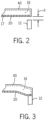
- MEMS device 10 is depicted in FIGS. 1-3 as a switch, it is contemplated that MEMS device 10 may be in the form of any of a number of different MEMS device, such as a resonator, an inertial sensor or a test probe, for example, according to other examples.
- the MEMS device 10 includes a substrate contact 12 (included when the MEMS device is a switch), which comprises a conductive material (e.g., metal).
- MEMS device 10 also includes a free-standing and suspended mechanical MEMS structure 14 that comprises a free-standing structure/mechanical element 16 - such as a beam - with the free-standing structure 16 having a cantilevered portion 18 that extends over contact 12, and with an underside or bottom surface 17 of the free-standing structure 16 being covered by a seed layer 20 that is mechanically coupled to and electrically connected with the structure, as will be discussed in greater detail below.
- the free-standing structure 16 is supported by an anchor portion 22, from which the cantilevered portion 18 extends, and which may be integrated with the free-standing structure 16.
- the anchor portion 22 serves to connect the cantilevered portion 18 of the free-standing structure 16 to an underlying support structure, such as a conductive mount 21 formed on a substrate 24.
- the substrate 24 may be formed of any of a number of materials suitable for MEMS device fabrication, including silicon and silicon-based substrates (e.g., silicon carbide (SiC)), fused silica or glass, for example.
- the free-standing MEMS structure 14 may constitute a portion of a microelectromechanical or nanoelectromechanical device or a MEMS device 10.
- the contact 12 and free-standing structure 16 may have dimensions on the order of ones or tens of nanometers or micrometers.
- the free-standing structure 16 may have a surface area-to-volume ratio that is greater than or equal to 10 8 m -1 , while in another embodiment the ratio may be closer to 10 3 m -1 .
- the free-standing structure 16 can be configured to be selectively moveable between a first, non-contacting or "open” position, shown in FIG. 2 , in which the free-standing structure 16 (and seed layer 20) is separated from the contact 12 by a separation distance d, and a second, contacting or “closed” position, shown in FIG. 3 , in which the free-standing structure 16 (and seed layer 20) comes into electrical contact with the contact 12.
- seed layer 20 acts as the electrical contact for free-standing structure 16.
- seed layer 20 electrically couples free-standing structure 16 and contact 12 when seed layer 20 comes into mechanical contact and electrical communication with electrical contact 12.
- the free-standing structure 16 and seed layer 20 can be configured to undergo deformation when moving between the contacting and non-contacting positions, such that the free-standing structure 16 and seed layer 20 are naturally disposed (i.e., in the absence of externally applied forces) in the non-contacting position and may be deformed so as to occupy the contacting position while storing mechanical energy therein.
- the undeformed configuration of the free-standing structure 16 and seed layer 20 may be the contacting position.
- the MEMS device 10 may also include an electrode 26 which, when appropriately charged, provides a potential difference between the electrode 26 and the free-standing structure 16 and seed layer 20, resulting in an electrostatic force that pulls the free-standing structure 16 and seed layer 20 toward the electrode 26 and against the contact 12.
- an electrode 26 which, when appropriately charged, provides a potential difference between the electrode 26 and the free-standing structure 16 and seed layer 20, resulting in an electrostatic force that pulls the free-standing structure 16 and seed layer 20 toward the electrode 26 and against the contact 12.
- the electrostatic force deforms the free-standing structure 16 and seed layer 20 and thereby displaces the free-standing structure 16 and seed layer 20 from the non-contacting (i.e., open or nonconducting) position shown in FIG. 2 to the contacting (i.e., closed or conducting) position shown in FIG. 3 .
- the electrode 26 may act as a "gate” with respect to the MEMS device 10, with voltages (referred to as “gate voltages") applied to the electrode 26 serving to control the opening or closing of the MEMS structure 14.
- the electrode 26 may be in communication with a gate voltage source 28, so that a gate voltage V G may be selectively applied to the electrode 26.
- the contact 12, free-standing structure 16, and seed layer 20 are components of the circuit 30.
- the exemplary circuit 30 has a first side 32 and a second side 34 that, when disconnected from one another, are at different electric potentials relative to one another (as where only one of the sides is connected to a power source 36).
- the contact 12 and free-standing structure 16, by way of seed layer 20, can be respectively connected to either of the sides 32, 34 of the circuit 30, such that deformation of the free-standing structure 16 and seed layer 20 between the first and second positions acts to respectively pass and interrupt a current therethrough.
- the free-standing structure 16 and seed layer 20 may be repeatedly moved into and out of contact with the contact 12 at a frequency (either uniform or non-uniform) that is determined by the application for which the MEMS structure 14 is utilized.
- the voltage difference between the contact 12 and free-standing structure 16 is referred to as the "stand-off voltage.”
- the free-standing structure 16 and seed layer 20 may be in communication (e.g., via the anchor structure 22) with the power source 36, and the contact 12 may be in communication with an electrical load 38 having a load resistance R L .
- the power source 36 may be operated as a voltage source or a current source.
- the free-standing structure 16 and seed layer 20 act as an electrical contact (i.e., ohmic contact), allowing a load current to flow from the power source 36 through the free-standing structure 16 and seed layer 20, into the contact 12 and to the electrical load 38 when the free-standing structure 16 and seed layer 20 are in the contacting position, and otherwise disrupting the electrical path and preventing the flow of current from the power source to the load when the free-standing structure 16 and seed layer 20 are in the non-contacting position.
- an electrical contact i.e., ohmic contact
- the above-described MEMS structure 14 could be utilized as part of a circuit including other switch structures, whether similar or dissimilar in design, in order to increase the current and voltage capacity of the overall circuit.
- Such switch structures could be configured in series or in parallel to facilitate an even distribution of stand-off voltage when the switch structures are open and an even distribution of current when the switch structures are closed.
- the refractory metal and/or refractory metal alloy from which seed layer 20 is formed may include one or more of ruthenium, tantalum, niobium, rhodium, molybdenum, tungsten, vanadium, chromium, zirconium, hafnium and/or alloys of the above.
- the free-standing structure 16 is formed on seed layer 20 via an electroplating process, with the seed layer 20 being subsequently being left intact on the bottom surface 17 of free-standing structure 16 upon completion of fabrication of the MEMS structure 14.
- the free-standing structure 16 and the seed layer 20 form a free-standing and suspended metal MEMS structure 14 that is resistant to stresses imposed on the MEMS structure during fabrication and subsequent operation, with the specific properties of the MEMS structure being tailorable based on the specific materials from which the free-standing structure 16 and seed layer 20 are formed and based on the dimensions of the free-standing structure 16 and seed layer 20.
- the thickness of free-standing structure 16 is substantially greater than the thickness of seed layer 20, such that the bending force related to the film stress does affect the planarity of the free-standing structure (i.e., beam) - with the thickness of the seed layer 20 being limited/selected such that the product of the residual stress in the free-standing MEMS structure ( ⁇ ) and the thickness of the structure is > 3x that of the product of the residual stress and thickness of the seed layer ( ⁇ MEMS ⁇ t MEMS > 3 ⁇ SEED ⁇ t SEED ).
- the mechanical and electrical properties of MEMS structure 14 are defined by the material of metal free-standing structure 16, not the material of seed layer 20.
- the seed layer 20 is further configured to provide a mechanically robust and electrically stable ohmic contact between the free-standing structure 16 and the contact 12. That is, as the seed layer is formed of a refractory metal or refractory alloy exhibiting properties such as melting temperature above 1850° C and a melting voltage above 0.4 V, the seed material is resistant to mechanical wear resulting from repeated physical impact with the substrate contact 12, and exhibits increased longevity when exposed to high temperatures (e.g., joule heating) and electrical discharges between the free-standing structure 16 and the contact 12. Accordingly, the seed layer 20 is able to increase longevity of the free-standing structure 16 and increase reliability of the MEMS switch.
- a refractory metal or refractory alloy exhibiting properties such as melting temperature above 1850° C and a melting voltage above 0.4 V
- the seed material is resistant to mechanical wear resulting from repeated physical impact with the substrate contact 12, and exhibits increased longevity when exposed to high temperatures (e.g., joule heating) and electrical discharges between the free-standing structure 16 and the
- the MEMS structure 14 can further comprise a protective layer 40 formed on one or more remaining exposed surfaces of free-standing structure 16 (i.e., surfaces other than bottom surface 17).
- protective layer 40 is applied to the exposed surfaces of free-standing structure 16 in order to surround the beam. The inclusion of seed layer 20 and protective layer 40 on free-standing structure 16 collectively serves to further increase the structural integrity of the free-standing structure 16 as well as provide chemical protection to the free-standing structure 16.
- MEMS structure 14 may be exposed to etchants/chemicals used in micro- and nanofabrications, such as etchants employed in wet etching, with exposure of free-standing structure 16 to chemicals in the wet etching process potentially resulting in irreversible damage to free-standing structure 16 and, as a result, its structural integrity during operation.
- etchants/chemicals used in micro- and nanofabrications such as etchants employed in wet etching
- the surrounding of free-standing structure 16 by seed layer 20 and protective layer 40 serves to protect the free-standing structure 16 from chemical attack during wet etching.
- the refractory metal and/or metal alloy (e.g., ruthenium, tantalum, niobium, rhodium, molybdenum, tungsten, titanium-tungsten alloy, etc.) from which seed layer 20 and protective layer 40 are formed is/are resistant to etchants/chemicals used in micro- and nanofabrications, including but not limited to sulfuric acid, hydrofluoric acid, buffered oxide, hydrogen peroxide and alkali photoresist developer solutions.
- seed layer 20 and protective layer protect free-standing structure 16, and the resulting MEMS structure 14, from both deformation due to high temperatures and chemical attack due to wet etching.
- a substrate 24 is initially provided on which the MEMS structure 14 is to be formed, with the substrate 24 being formed of any of a number of materials suitable for MEMS device fabrication, including silicon and silicon-based substrates (e.g., silicon carbide (SiC)), fused silica and glass for example.
- silicon and silicon-based substrates e.g., silicon carbide (SiC)
- fused silica and glass for example.
- the conductive contact 12, electrode 26, and conductive mount 21 are formed on substrate 24.
- the conductive contact 12, electrode 26, and conductive mount 21 may be formed by applying a layer of conductive metallic material (e.g., gold, copper, etc.) onto substrate 24 and performing a subsequent etching to pattern the layer and form the conductive contact 12, electrode 26, and conductive mount 21.
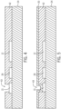
- a sacrificial release layer 42 is applied thereover in an area at which the free-standing structure 16 is to be formed.
- release layer 42 comprises SiO 2 (silicon dioxide); however, one skilled in the art would recognize that release layer 42 may comprise other materials, for example, but not limited to, a metal, ceramic, or polymer.
- seed layer 20 is applied on release layer 42, such as via a sputtering process or other suitable application process.
- seed layer 20 extends through an opening 43 in the release layer 42, in order to be in direct contact with conductive mount 21.
- Seed layer 20 comprises a refractory metal and/or refractory metal alloy material - which is defined herein as a metallic material exhibiting properties such as melting temperature above 1850° C and a melting voltage above 0.4 V.
- the refractory metal/metal alloy applied may thus be one or more of ruthenium, tantalum, niobium, rhodium, molybdenum, tungsten, vanadium, chromium, zirconium, hafnium and/or alloys of the above, for example.
- seed layer 20 will be left intact on the bottom surface 17 of free-standing structure 16 in order to provide a mechanically robust and electrically stable ohmic contact with the contact 12, as the refractory metal of the seed layer 20 is resistant to mechanical wear and exhibits increased longevity when exposed to high temperatures and electrical discharges.
- the seed layer 20 may also provide protection from damage due to chemical attacks during further wet etching occurring during fabrication therof.
- a patterned photoresist mask 44 is applied to seed layer 20.
- photoresist mask 44 includes at least one opening 46, wherein seed layer 20 remains exposed.
- Cantilever free-standing structure 16 is then formed by electroplating a metallic material onto seed layer 20 within the at least one opening 46 of photoresist mask 44.
- the metallic material used to form free-standing structure 16 comprises a NiW (nickel-tungsten) alloy; however, it is contemplated that the material of free-standing structure 16 may be any material judged appropriate by one skilled in the art.
- free-standing structure 16 includes at least one unexposed side 50 (underside 17 of free-standing structure), wherein seed layer 20 is in contact with free-standing structure 16, and further includes at least one exposed side 52, wherein free-standing structure 16 is not in contact with any other elements, and, therefore, is exposed.
- release layer 42 and the portion of seed layer 20 not in contact with free-standing structure 16 is removed by etching processes known in the art in micro- and nanofabrication.
- a wet etching process may use sulfuric acid, hydrofluoric acid, buffered oxide etch, and/or hydrogen peroxide.
- a dry etching process using known dry etching techniques such as reactive ion etching, sputter etching, and vapor phase etching, may be used to remove release layer 42 and the portion of seed layer 20 not in contact with free-standing structure 16.
- protective layer 40 applied to at least one of the at least one exposed side 52 of free-standing structure 16 is illustrated, according to one example.
- the inclusion of protective layer 40 (combined with seed layer 20) on free-standing structure 16 serves to provide chemical protection to the free-standing structure 16 with regard to etchants/chemicals used in micro- and nanofabrications, such as etchants employed in wet etching, with exposure of free-standing structure 16 to chemicals in the wet etching process potentially resulting in irreversible damage to free-standing structure 16 and, as a result, its structural integrity during operation.
- etchants/chemicals used in micro- and nanofabrications such as etchants employed in wet etching
- the addition of protective layer 40 is optional and not a requirement for all examples.
- examples thus provide a MEMS device and associated free-standing and suspended metal MEMS structure that is resistant to stresses imposed on the MEMS structure during fabrication and subsequent operation, with the specific properties of the MEMS structure being tailorable based on the specific materials from which the free-standing structure and seed layer are formed and based on the dimensions/thicknesses of the free-standing structure and seed layer.
- the refractory seed layer is the layer onto which the free-standing MEMS structure will be deposited by electroplating and is constructed such that the mechanical and electrical properties of the free-standing and suspended electroplated metal MEMS structure are defined by the material of the free-standing structure.
- the seed layer provides an ohmic contact between the free-standing structure and a conductive contact on the substrate that is resistant to mechanical wear and exhibits increased longevity when exposed to high temperatures and electrical discharges, as the refractory metal of the seed layer has a melting temperature above 1850° C and a melting voltage above 0.4 V.
- a micro-electrical-mechanical system (MEMS) device includes a substrate and a free-standing and suspended electroplated metal MEMS structure formed on the substrate.
- the free-standing and suspended electroplated metal MEMS structure includes a metal mechanical element mechanically coupled to the substrate and a seed layer mechanically coupled to and in electrical communication with the mechanical element, the seed layer comprising at least one of a refractory metal and a refractory metal alloy, wherein a thickness of the mechanical element is substantially greater than a thickness of the seed layer such that the mechanical and electrical properties of the free-standing and suspended electroplated metal MEMS structure are defined by the material properties of the mechanical element
- a method of creating a micro-electrical-mechanical system (MEMS) device includes providing a substrate and forming a free-standing MEMS structure on the substrate.
- Forming the free-standing MEMS structure includes applying a sacrificial release layer on a portion of the substrate, applying a layer of seed metal over the substrate and the sacrificial release layer, wherein the seed metal comprises at least one of a refractory metal and a refractory metal alloy, applying a photoresist layer on a portion of the layer of seed metal, electroplating a metallic material onto the layer of seed metal not covered by the photoresist layer to form a free-standing structure, and removing the photoresist layer, the sacrificial release layer, and a portion of the layer of seed metal not in contact with the free-standing structure, such that the beam is cantilevered over the substrate, wherein a portion of the layer of seed metal in contact with the free-standing structure remains on an underside of the free-standing structure subsequent to the
- a free-standing and suspended metal micro-electro-mechanical system (MEMS) structure of a MEMS device is fabricated by applying a sacrificial release layer on a portion of a substrate, applying a seed layer of refractory metal over the substrate and the sacrificial release layer, applying a photoresist layer on a portion of the seed layer, electroplating a metallic material onto the seed layer in an area not covered by the photoresist layer to form a free-standing structure, the free-standing structure being mechanically coupled to and electrically connected with the seed layer, and removing the photoresist layer, the sacrificial release layer, and a portion of the seed layer such that a layer of refractory metal remains on an underside of the free-standing structure to collectively form a free-standing and suspended metal MEMS structure on the substrate.
- MEMS micro-electro-mechanical system
Landscapes
- Engineering & Computer Science (AREA)
- Microelectronics & Electronic Packaging (AREA)
- Manufacturing & Machinery (AREA)
- Computer Hardware Design (AREA)
- Chemical & Material Sciences (AREA)
- Analytical Chemistry (AREA)
- Physics & Mathematics (AREA)
- General Physics & Mathematics (AREA)
- Mechanical Engineering (AREA)
- Micromachines (AREA)
Claims (13)
- Vorrichtung (10) für ein mikro-elektromechanisches System (MEMS), umfassend:ein Substrat (24); undeine freistehende und aufgehängte elektroplattierte Metall-MEMS-Struktur (14), die auf dem Substrat ausgebildet ist und Folgendes umfasst:ein mechanisches Metallelement (16), das mechanisch mit dem Substrat (24) gekoppelt ist, wobei das mechanische Metallelement (16) einen freitragenden Abschnitt (18) aufweist; undeine Keimschicht (20), die mechanisch mit dem mechanischen Element (16) gekoppelt ist und mit diesem in elektrischer Kommunikation steht, wobei die Keimschicht (20) auf einer Unterseite des mechanischen Elements (16), die dem Substrat (24) zugewandt ist, intakt gelassen wird, wobei die Keimschicht (20) mindestens ein feuerfestes Metall oder eine feuerfeste Metalllegierung umfasst;wobei eine Dicke des mechanischen Elements (16) im Wesentlichen größer ist als eine Dicke der Keimschicht (20), sodass die mechanischen und elektrischen Eigenschaften der freistehenden und aufgehängten elektroplattierten Metall-MEMS-Struktur (14) durch die Materialeigenschaften des mechanischen Elements (16) definiert sind,dadurch gekennzeichnet, dass die Dicke der Keimschicht (20) so gewählt ist, dass das Produkt aus einer Restspannung in dem mechanischen Element (16) und der Dicke des mechanischen Elements (16) größer ist als das Dreifache des Produkts aus der Restspannung in der Keimschicht (20) und der Dicke der Keimschicht (20).
- MEMS-Vorrichtung (10) nach Anspruch 1, wobei das mechanische Element (16) aus einer Nickel-Wolfram-Legierung zusammengesetzt ist.
- MEMS-Vorrichtung (10) nach Anspruch 1, wobei die MEMS-Vorrichtung (10) ein Schalter ist, wobei der Schalter ferner mindestens einen leitenden Kontakt (12) umfasst, der auf dem Substrat (24) ausgebildet ist, und wobei das mechanische Element (16) einen über den leitenden Kontakt (12) freitragenden Träger umfasst;
wobei die Keimschicht (20) einen ohmschen Kontakt zwischen dem Träger und dem mindestens einen leitenden Kontakt (12) bereitstellt, wenn sich der Träger in einer Kontaktierungsposition befindet. - MEMS-Vorrichtung (10) nach einem der vorhergehenden Ansprüche, wobei das feuerfeste Metall und/oder die feuerfeste Metalllegierung der Keimschicht (20) eine Schmelzspannung von mehr als 0,4 V und eine Schmelztemperatur von mehr als 1850 °C aufweist.
- MEMS-Vorrichtung (10) nach einem der vorhergehenden Ansprüche, ferner umfassend eine Schutzschicht (40), die mechanisch mit dem mechanischen Element (16) gekoppelt ist, wobei die Schutzschicht (40) auf mindestens einer zusätzlichen Oberfläche des mechanischen Elements (16) ausgebildet ist, die nicht von der Keimschicht (20) bedeckt ist.
- MEMS-Vorrichtung (10) nach einem der vorhergehenden Ansprüche, wobei das feuerfeste Metall und die feuerfeste Metalllegierung eines oder mehrere von Ruthenium, Tantal, Niob, Rhodium, Molybdän, Wolfram, Vanadium, Chrom, Zirkonium, Hafnium und/oder Legierungen davon umfasst.
- MEMS-Vorrichtung (10) nach einem der vorhergehenden Ansprüche, wobei mindestens eines von dem feuerfesten Metall und der feuerfesten Metalllegierung resistent gegen Ätzmittel ist, die bei der Mikro- und Nanofabrikation verwendet werden, wobei die Ätzmittel eines oder mehrere von Schwefelsäure, Flusssäure, gepuffertem Oxid, Wasserstoffperoxid und alkalischen Photoresistentwicklerlösungen umfassen.
- MEMS-Vorrichtung (10) nach einem der vorhergehenden Ansprüche, wobei die MEMS-Vorrichtung (10) ein Trägheitssensor ist.
- Verfahren zum Herstellen einer Vorrichtung (10) für ein mikro-elektromechanisches System (MEMS), umfassend:Bereitstellen eines Substrats (24); undBilden einer freistehenden Metall-MEMS-Struktur (14) auf dem Substrat (24), wobei Bilden der freistehenden Metall-MEMS-Struktur Folgendes umfasst:Aufbringen einer Opferfreisetzungsschicht (42) auf einen Abschnitt des Substrats (24);Aufbringen einer Schicht aus Keimmetall (20) über dem Substrat (24) und der Opferfreisetzungsschicht (42), wobei sich das Keimmetall (20) durch eine Öffnung (43) in der Opferfreisetzungsschicht (42) erstreckt, um über eine leitende Halterung (21) mit dem Substrat (24) in Kontakt zu sein, wobei das Keimmetall (20) mindestens eines von einem feuerfesten Metall und einer feuerfesten Metalllegierung umfasst;Aufbringen einer Photoresistschicht (44) auf einen Abschnitt der Schicht aus Keimmetall (20);Elektroplattieren eines metallischen Materials auf die nicht von der Photoresistschicht (44) bedeckte Schicht aus Keimmetall (20), um eine freistehende Struktur (16) zu bilden; undEntfernen der Photoresistschicht (44), der Opferfreisetzungsschicht (16) und eines Abschnitts der Schicht aus Keimmetall, der nicht in Kontakt mit der freistehenden Struktur (16) steht, sodass die freistehende Struktur über dem Substrat (24) freitragend ist;wobei ein Abschnitt der Schicht aus Keimmetall (20), der mit der freistehenden Struktur (16) in Kontakt ist, auf einer Unterseite der freistehenden Struktur (16) verbleibt, nachdem die Photoresistschicht (44), die Opferfreisetzungsschicht (42) und der Abschnitt der Schicht aus Keimmetall (20), der nicht in Kontakt mit der freistehenden Struktur ist, entfernt wurden,wobei eine Dicke der freistehenden Struktur (16) im Wesentlichen größer ist als eine Dicke der Schicht aus Keimmetall (20), sodass die mechanischen und elektrischen Eigenschaften der freistehenden Metall-MEMS-Struktur (14) durch das elektroplattierte metallische Material der freistehenden Struktur (16) definiert sind,wobei die Dicke der Keimschicht (20) so gewählt ist, dass das Produkt aus einer Restspannung in dem mechanischen Element (16) und der Dicke des mechanischen Elements (16) größer ist als das Dreifache des Produkts aus der Restspannung in der Keimschicht (20) und der Dicke der Keimschicht (20).
- Verfahren nach Anspruch 9, wobei Bilden der MEMS-Struktur (14) ferner Beschichten mindestens einer zusätzlichen Seite der freistehenden Struktur (16) mit einer Schutzschicht (40) umfasst, wobei die Schutzschicht (40) ein Material umfasst, das gegen Beschädigung oder Ätzen während eines Herstellungsprozesses beständig ist, und wobei Beschichten der mindestens zusätzlichen Seite der freistehenden Struktur (16) mit einer Schutzschicht (40) Beschichten jeder freiliegenden Seite der freistehenden Struktur (16) mit der Schutzschicht (40) umfasst.
- Verfahren nach Anspruch 9 oder 10, wobei Elektroplattieren des metallischen Materials auf die Schicht aus Keimmetall (20) Elektroplattieren einer Nickel-Wolfram-Legierung umfasst.
- Verfahren nach einem der Ansprüche 9 bis 11, wobei Entfernen der Opferfreisetzungsschicht (42) Durchführen eines Nassätzens durch Anwendung von mindestens einem von Schwefelsäure, Fluorwasserstoffsäure, gepuffertem Oxid und Wasserstoffperoxid umfasst; und
wobei die Schicht aus Keimmetall (20) gegen Schwefelsäure, Fluorwasserstoffsäure, gepuffertes Oxid und Wasserstoffperoxid und gegen alkalische Photoresistentwicklerlösungen beständig ist. - Verfahren nach einem der Ansprüche 9 bis 12, ferner umfassend Bilden einer leitenden Schicht auf dem Substrat, wobei die leitende Schicht mindestens einen MEMS-Kontakt (12) umfasst, wobei die Schicht aus Keimmaterial (20) als ohmscher Kontakt zwischen der freistehenden Struktur (16) und dem mindestens einen MEMS-Kontakt (12) fungiert, wenn sich die freistehende Struktur (16) in einer Kontaktierungsposition befindet, wobei die Schicht aus Keimmaterial (20) eine Schmelzspannung von mehr als 0,4 V und eine Schmelztemperatur von mehr als 1850 °C aufweist.
Applications Claiming Priority (2)
| Application Number | Priority Date | Filing Date | Title |
|---|---|---|---|
| US14/844,132 US9845235B2 (en) | 2015-09-03 | 2015-09-03 | Refractory seed metal for electroplated MEMS structures |
| PCT/US2016/041954 WO2017058335A1 (en) | 2015-09-03 | 2016-07-13 | Refractory seed metal for electroplated mems structures |
Publications (2)
| Publication Number | Publication Date |
|---|---|
| EP3344574A1 EP3344574A1 (de) | 2018-07-11 |
| EP3344574B1 true EP3344574B1 (de) | 2023-04-12 |
Family
ID=57851320
Family Applications (1)
| Application Number | Title | Priority Date | Filing Date |
|---|---|---|---|
| EP16829011.2A Active EP3344574B1 (de) | 2015-09-03 | 2016-07-13 | Feuerfestes keimmetall für elektroplattierte mems-strukturen |
Country Status (5)
| Country | Link |
|---|---|
| US (1) | US9845235B2 (de) |
| EP (1) | EP3344574B1 (de) |
| JP (1) | JP6820913B2 (de) |
| TW (1) | TWI701212B (de) |
| WO (1) | WO2017058335A1 (de) |
Families Citing this family (5)
| Publication number | Priority date | Publication date | Assignee | Title |
|---|---|---|---|---|
| US10580605B2 (en) * | 2015-11-23 | 2020-03-03 | University Of Utah Research Foundation | Very low power microelectromechanical devices for the internet of everything |
| US10825628B2 (en) | 2017-07-17 | 2020-11-03 | Analog Devices Global Unlimited Company | Electromagnetically actuated microelectromechanical switch |
| CN113716518B (zh) * | 2021-08-02 | 2024-11-22 | 三明学院 | 一种GaN同质悬臂梁结构及其制备方法 |
| US20250056874A1 (en) * | 2023-08-11 | 2025-02-13 | Taiwan Semiconductor Manufacturing Company, Ltd. | Power gating using nanoelectromechanical systems (nems) in back end of line (beol) |
| US20260015222A1 (en) * | 2024-07-12 | 2026-01-15 | Menlo Microsystems, Inc. | Two stage plating for reduced Ni and NiO layer formation |
Family Cites Families (24)
| Publication number | Priority date | Publication date | Assignee | Title |
|---|---|---|---|---|
| US6221763B1 (en) | 1999-04-05 | 2001-04-24 | Micron Technology, Inc. | Method of forming a metal seed layer for subsequent plating |
| US6136707A (en) | 1999-10-02 | 2000-10-24 | Cohen; Uri | Seed layers for interconnects and methods for fabricating such seed layers |
| JP4292532B2 (ja) * | 2002-04-24 | 2009-07-08 | 株式会社沖センサデバイス | 機構デバイスの製造方法、機構デバイスおよびマイクロリードスイッチ |
| US7202764B2 (en) | 2003-07-08 | 2007-04-10 | International Business Machines Corporation | Noble metal contacts for micro-electromechanical switches |
| US7176047B2 (en) | 2004-01-30 | 2007-02-13 | Taiwan Semiconductor Manufacturing Co., Ltd. | Method for manufacturing MEMS structures |
| US20060063025A1 (en) | 2004-04-07 | 2006-03-23 | Jing-Yi Huang | Method and system for making thin metal films |
| US20050277281A1 (en) | 2004-06-10 | 2005-12-15 | Dubin Valery M | Compliant interconnect and method of formation |
| US7956429B1 (en) * | 2007-08-02 | 2011-06-07 | Rf Micro Devices, Inc. | Insulator layer based MEMS devices |
| US8159056B1 (en) * | 2008-01-15 | 2012-04-17 | Rf Micro Devices, Inc. | Package for an electronic device |
| US8320038B2 (en) | 2008-12-16 | 2012-11-27 | Silicon Light Machines Corporation | Method of fabricating an integrated device |
| US8445306B2 (en) | 2008-12-24 | 2013-05-21 | International Business Machines Corporation | Hybrid MEMS RF switch and method of fabricating same |
| US8957485B2 (en) | 2009-01-21 | 2015-02-17 | Cavendish Kinetics, Ltd. | Fabrication of MEMS based cantilever switches by employing a split layer cantilever deposition scheme |
| JP5341579B2 (ja) * | 2009-03-13 | 2013-11-13 | 日本電信電話株式会社 | 微細構造体の製造方法 |
| US20100291410A1 (en) | 2009-05-13 | 2010-11-18 | Spatial Photonics, Inc. | Corrosion Protection and Lubrication of MEMS Devices |
| US8826529B2 (en) | 2009-09-23 | 2014-09-09 | General Electric Company | Method of forming a micro-electromechanical system device |
| US8354899B2 (en) * | 2009-09-23 | 2013-01-15 | General Electric Company | Switch structure and method |
| JP2011097038A (ja) * | 2009-10-02 | 2011-05-12 | Ibiden Co Ltd | セラミック配線基板およびその製造方法 |
| JP2012086315A (ja) * | 2010-10-20 | 2012-05-10 | Nippon Telegr & Teleph Corp <Ntt> | 微細可動構造体の製造方法および微細可動構造体 |
| SG11201402261SA (en) * | 2011-12-07 | 2014-08-28 | Georgia Tech Res Inst | Packaging compatible wafer level capping of mems devices |
| US10665503B2 (en) | 2012-04-26 | 2020-05-26 | Applied Materials, Inc. | Semiconductor reflow processing for feature fill |
| US8691607B2 (en) | 2012-06-07 | 2014-04-08 | Texas Instruments Incorporated | Hermetically sealed MEMS device and method of fabrication |
| JP2014075193A (ja) * | 2012-10-02 | 2014-04-24 | Fujitsu Ltd | 電子装置の製造方法 |
| JP6154729B2 (ja) * | 2013-10-28 | 2017-06-28 | 富士フイルム株式会社 | 圧電体素子の製造方法 |
| CN104445044B (zh) * | 2014-12-03 | 2016-08-17 | 中国科学院上海微系统与信息技术研究所 | 偏离(111)硅片解理晶向的高强度悬臂梁结构及制作方法 |
-
2015
- 2015-09-03 US US14/844,132 patent/US9845235B2/en active Active
-
2016
- 2016-07-13 JP JP2018511120A patent/JP6820913B2/ja active Active
- 2016-07-13 WO PCT/US2016/041954 patent/WO2017058335A1/en not_active Ceased
- 2016-07-13 EP EP16829011.2A patent/EP3344574B1/de active Active
- 2016-08-22 TW TW105126789A patent/TWI701212B/zh active
Also Published As
| Publication number | Publication date |
|---|---|
| JP2018527206A (ja) | 2018-09-20 |
| TW201722836A (zh) | 2017-07-01 |
| US9845235B2 (en) | 2017-12-19 |
| EP3344574A1 (de) | 2018-07-11 |
| US20170066645A1 (en) | 2017-03-09 |
| WO2017058335A1 (en) | 2017-04-06 |
| TWI701212B (zh) | 2020-08-11 |
| JP6820913B2 (ja) | 2021-01-27 |
Similar Documents
| Publication | Publication Date | Title |
|---|---|---|
| US9845235B2 (en) | Refractory seed metal for electroplated MEMS structures | |
| US7471176B2 (en) | Micro electromechanical system switch | |
| US8420427B2 (en) | Methods for implementation of a switching function in a microscale device and for fabrication of a microscale switch | |
| EP1008161B1 (de) | Mikromechanische vorrichtungen mit thermischer bogentraverse und zugehörige herstellungsverfahren | |
| Czaplewski et al. | RF MEMS Switches With $\hbox {RuO} _ {2} $–$\hbox {Au} $ Contacts Cycled to 10 Billion Cycles | |
| US8054147B2 (en) | High voltage switch and method of making | |
| US7276991B2 (en) | Multiple switch MEMS structure and method of manufacture | |
| US20110067983A1 (en) | Switch structure and method | |
| US8207460B2 (en) | Electrostatically actuated non-latching and latching RF-MEMS switch | |
| JP2009009884A (ja) | Memsスイッチ及びその製造方法 | |
| CA2977788C (en) | Electromechanical system substrate attachment for reduced thermal deformation | |
| US20090314616A1 (en) | Swtich, Method and System For Switching The State of a Signal Path | |
| US20090134522A1 (en) | Micro-Electromechanical System Memory Device and Method of Making the Same | |
| Lee et al. | Micro-electro-mechanical relays-design concepts and process demonstrations | |
| Lin et al. | Lateral flexure contact on CMOS MEMS electrothermal metal-metal contact switch by platinum ALD sidewall patterning | |
| Driesen et al. | Nickel-plated thermal switch with electrostatic latch | |
| Oberhammer et al. | Mechanically tri-stable in-line single-pole-double-throw all-metal switch | |
| Khushalani et al. | Fabrication of MEMS Cantilever Switch |
Legal Events
| Date | Code | Title | Description |
|---|---|---|---|
| STAA | Information on the status of an ep patent application or granted ep patent |
Free format text: STATUS: UNKNOWN |
|
| STAA | Information on the status of an ep patent application or granted ep patent |
Free format text: STATUS: THE INTERNATIONAL PUBLICATION HAS BEEN MADE |
|
| PUAI | Public reference made under article 153(3) epc to a published international application that has entered the european phase |
Free format text: ORIGINAL CODE: 0009012 |
|
| STAA | Information on the status of an ep patent application or granted ep patent |
Free format text: STATUS: REQUEST FOR EXAMINATION WAS MADE |
|
| 17P | Request for examination filed |
Effective date: 20180403 |
|
| AK | Designated contracting states |
Kind code of ref document: A1 Designated state(s): AL AT BE BG CH CY CZ DE DK EE ES FI FR GB GR HR HU IE IS IT LI LT LU LV MC MK MT NL NO PL PT RO RS SE SI SK SM TR |
|
| AX | Request for extension of the european patent |
Extension state: BA ME |
|
| DAV | Request for validation of the european patent (deleted) | ||
| DAX | Request for extension of the european patent (deleted) | ||
| STAA | Information on the status of an ep patent application or granted ep patent |
Free format text: STATUS: EXAMINATION IS IN PROGRESS |
|
| 17Q | First examination report despatched |
Effective date: 20210223 |
|
| GRAP | Despatch of communication of intention to grant a patent |
Free format text: ORIGINAL CODE: EPIDOSNIGR1 |
|
| STAA | Information on the status of an ep patent application or granted ep patent |
Free format text: STATUS: GRANT OF PATENT IS INTENDED |
|
| INTG | Intention to grant announced |
Effective date: 20221219 |
|
| GRAS | Grant fee paid |
Free format text: ORIGINAL CODE: EPIDOSNIGR3 |
|
| GRAA | (expected) grant |
Free format text: ORIGINAL CODE: 0009210 |
|
| STAA | Information on the status of an ep patent application or granted ep patent |
Free format text: STATUS: THE PATENT HAS BEEN GRANTED |
|
| AK | Designated contracting states |
Kind code of ref document: B1 Designated state(s): AL AT BE BG CH CY CZ DE DK EE ES FI FR GB GR HR HU IE IS IT LI LT LU LV MC MK MT NL NO PL PT RO RS SE SI SK SM TR |
|
| REG | Reference to a national code |
Ref country code: GB Ref legal event code: FG4D |
|
| REG | Reference to a national code |
Ref country code: CH Ref legal event code: EP |
|
| REG | Reference to a national code |
Ref country code: DE Ref legal event code: R096 Ref document number: 602016078821 Country of ref document: DE |
|
| REG | Reference to a national code |
Ref country code: IE Ref legal event code: FG4D |
|
| REG | Reference to a national code |
Ref country code: AT Ref legal event code: REF Ref document number: 1559688 Country of ref document: AT Kind code of ref document: T Effective date: 20230515 |
|
| REG | Reference to a national code |
Ref country code: LT Ref legal event code: MG9D |
|
| REG | Reference to a national code |
Ref country code: NL Ref legal event code: MP Effective date: 20230412 |
|
| REG | Reference to a national code |
Ref country code: AT Ref legal event code: MK05 Ref document number: 1559688 Country of ref document: AT Kind code of ref document: T Effective date: 20230412 |
|
| PG25 | Lapsed in a contracting state [announced via postgrant information from national office to epo] |
Ref country code: NL Free format text: LAPSE BECAUSE OF FAILURE TO SUBMIT A TRANSLATION OF THE DESCRIPTION OR TO PAY THE FEE WITHIN THE PRESCRIBED TIME-LIMIT Effective date: 20230412 |
|
| PG25 | Lapsed in a contracting state [announced via postgrant information from national office to epo] |
Ref country code: SE Free format text: LAPSE BECAUSE OF FAILURE TO SUBMIT A TRANSLATION OF THE DESCRIPTION OR TO PAY THE FEE WITHIN THE PRESCRIBED TIME-LIMIT Effective date: 20230412 Ref country code: PT Free format text: LAPSE BECAUSE OF FAILURE TO SUBMIT A TRANSLATION OF THE DESCRIPTION OR TO PAY THE FEE WITHIN THE PRESCRIBED TIME-LIMIT Effective date: 20230814 Ref country code: NO Free format text: LAPSE BECAUSE OF FAILURE TO SUBMIT A TRANSLATION OF THE DESCRIPTION OR TO PAY THE FEE WITHIN THE PRESCRIBED TIME-LIMIT Effective date: 20230712 Ref country code: ES Free format text: LAPSE BECAUSE OF FAILURE TO SUBMIT A TRANSLATION OF THE DESCRIPTION OR TO PAY THE FEE WITHIN THE PRESCRIBED TIME-LIMIT Effective date: 20230412 Ref country code: AT Free format text: LAPSE BECAUSE OF FAILURE TO SUBMIT A TRANSLATION OF THE DESCRIPTION OR TO PAY THE FEE WITHIN THE PRESCRIBED TIME-LIMIT Effective date: 20230412 |
|
| PG25 | Lapsed in a contracting state [announced via postgrant information from national office to epo] |
Ref country code: RS Free format text: LAPSE BECAUSE OF FAILURE TO SUBMIT A TRANSLATION OF THE DESCRIPTION OR TO PAY THE FEE WITHIN THE PRESCRIBED TIME-LIMIT Effective date: 20230412 Ref country code: PL Free format text: LAPSE BECAUSE OF FAILURE TO SUBMIT A TRANSLATION OF THE DESCRIPTION OR TO PAY THE FEE WITHIN THE PRESCRIBED TIME-LIMIT Effective date: 20230412 Ref country code: LV Free format text: LAPSE BECAUSE OF FAILURE TO SUBMIT A TRANSLATION OF THE DESCRIPTION OR TO PAY THE FEE WITHIN THE PRESCRIBED TIME-LIMIT Effective date: 20230412 Ref country code: LT Free format text: LAPSE BECAUSE OF FAILURE TO SUBMIT A TRANSLATION OF THE DESCRIPTION OR TO PAY THE FEE WITHIN THE PRESCRIBED TIME-LIMIT Effective date: 20230412 Ref country code: IS Free format text: LAPSE BECAUSE OF FAILURE TO SUBMIT A TRANSLATION OF THE DESCRIPTION OR TO PAY THE FEE WITHIN THE PRESCRIBED TIME-LIMIT Effective date: 20230812 Ref country code: HR Free format text: LAPSE BECAUSE OF FAILURE TO SUBMIT A TRANSLATION OF THE DESCRIPTION OR TO PAY THE FEE WITHIN THE PRESCRIBED TIME-LIMIT Effective date: 20230412 Ref country code: GR Free format text: LAPSE BECAUSE OF FAILURE TO SUBMIT A TRANSLATION OF THE DESCRIPTION OR TO PAY THE FEE WITHIN THE PRESCRIBED TIME-LIMIT Effective date: 20230713 Ref country code: AL Free format text: LAPSE BECAUSE OF FAILURE TO SUBMIT A TRANSLATION OF THE DESCRIPTION OR TO PAY THE FEE WITHIN THE PRESCRIBED TIME-LIMIT Effective date: 20230412 |
|
| PG25 | Lapsed in a contracting state [announced via postgrant information from national office to epo] |
Ref country code: FI Free format text: LAPSE BECAUSE OF FAILURE TO SUBMIT A TRANSLATION OF THE DESCRIPTION OR TO PAY THE FEE WITHIN THE PRESCRIBED TIME-LIMIT Effective date: 20230412 |
|
| REG | Reference to a national code |
Ref country code: DE Ref legal event code: R097 Ref document number: 602016078821 Country of ref document: DE |
|
| PG25 | Lapsed in a contracting state [announced via postgrant information from national office to epo] |
Ref country code: SK Free format text: LAPSE BECAUSE OF FAILURE TO SUBMIT A TRANSLATION OF THE DESCRIPTION OR TO PAY THE FEE WITHIN THE PRESCRIBED TIME-LIMIT Effective date: 20230412 |
|
| PG25 | Lapsed in a contracting state [announced via postgrant information from national office to epo] |
Ref country code: SM Free format text: LAPSE BECAUSE OF FAILURE TO SUBMIT A TRANSLATION OF THE DESCRIPTION OR TO PAY THE FEE WITHIN THE PRESCRIBED TIME-LIMIT Effective date: 20230412 Ref country code: SK Free format text: LAPSE BECAUSE OF FAILURE TO SUBMIT A TRANSLATION OF THE DESCRIPTION OR TO PAY THE FEE WITHIN THE PRESCRIBED TIME-LIMIT Effective date: 20230412 Ref country code: RO Free format text: LAPSE BECAUSE OF FAILURE TO SUBMIT A TRANSLATION OF THE DESCRIPTION OR TO PAY THE FEE WITHIN THE PRESCRIBED TIME-LIMIT Effective date: 20230412 Ref country code: EE Free format text: LAPSE BECAUSE OF FAILURE TO SUBMIT A TRANSLATION OF THE DESCRIPTION OR TO PAY THE FEE WITHIN THE PRESCRIBED TIME-LIMIT Effective date: 20230412 Ref country code: DK Free format text: LAPSE BECAUSE OF FAILURE TO SUBMIT A TRANSLATION OF THE DESCRIPTION OR TO PAY THE FEE WITHIN THE PRESCRIBED TIME-LIMIT Effective date: 20230412 Ref country code: CZ Free format text: LAPSE BECAUSE OF FAILURE TO SUBMIT A TRANSLATION OF THE DESCRIPTION OR TO PAY THE FEE WITHIN THE PRESCRIBED TIME-LIMIT Effective date: 20230412 |
|
| PLBE | No opposition filed within time limit |
Free format text: ORIGINAL CODE: 0009261 |
|
| STAA | Information on the status of an ep patent application or granted ep patent |
Free format text: STATUS: NO OPPOSITION FILED WITHIN TIME LIMIT |
|
| PG25 | Lapsed in a contracting state [announced via postgrant information from national office to epo] |
Ref country code: MC Free format text: LAPSE BECAUSE OF FAILURE TO SUBMIT A TRANSLATION OF THE DESCRIPTION OR TO PAY THE FEE WITHIN THE PRESCRIBED TIME-LIMIT Effective date: 20230412 |
|
| PG25 | Lapsed in a contracting state [announced via postgrant information from national office to epo] |
Ref country code: MC Free format text: LAPSE BECAUSE OF FAILURE TO SUBMIT A TRANSLATION OF THE DESCRIPTION OR TO PAY THE FEE WITHIN THE PRESCRIBED TIME-LIMIT Effective date: 20230412 |
|
| REG | Reference to a national code |
Ref country code: CH Ref legal event code: PL |
|
| REG | Reference to a national code |
Ref country code: BE Ref legal event code: MM Effective date: 20230731 |
|
| 26N | No opposition filed |
Effective date: 20240115 |
|
| PG25 | Lapsed in a contracting state [announced via postgrant information from national office to epo] |
Ref country code: LU Free format text: LAPSE BECAUSE OF NON-PAYMENT OF DUE FEES Effective date: 20230713 |
|
| GBPC | Gb: european patent ceased through non-payment of renewal fee |
Effective date: 20230713 |
|
| PG25 | Lapsed in a contracting state [announced via postgrant information from national office to epo] |
Ref country code: LU Free format text: LAPSE BECAUSE OF NON-PAYMENT OF DUE FEES Effective date: 20230713 |
|
| REG | Reference to a national code |
Ref country code: IE Ref legal event code: MM4A |
|
| PG25 | Lapsed in a contracting state [announced via postgrant information from national office to epo] |
Ref country code: CH Free format text: LAPSE BECAUSE OF NON-PAYMENT OF DUE FEES Effective date: 20230731 Ref country code: GB Free format text: LAPSE BECAUSE OF NON-PAYMENT OF DUE FEES Effective date: 20230713 |
|
| PG25 | Lapsed in a contracting state [announced via postgrant information from national office to epo] |
Ref country code: SI Free format text: LAPSE BECAUSE OF FAILURE TO SUBMIT A TRANSLATION OF THE DESCRIPTION OR TO PAY THE FEE WITHIN THE PRESCRIBED TIME-LIMIT Effective date: 20230412 |
|
| PG25 | Lapsed in a contracting state [announced via postgrant information from national office to epo] |
Ref country code: SI Free format text: LAPSE BECAUSE OF FAILURE TO SUBMIT A TRANSLATION OF THE DESCRIPTION OR TO PAY THE FEE WITHIN THE PRESCRIBED TIME-LIMIT Effective date: 20230412 Ref country code: IT Free format text: LAPSE BECAUSE OF FAILURE TO SUBMIT A TRANSLATION OF THE DESCRIPTION OR TO PAY THE FEE WITHIN THE PRESCRIBED TIME-LIMIT Effective date: 20230412 Ref country code: FR Free format text: LAPSE BECAUSE OF NON-PAYMENT OF DUE FEES Effective date: 20230731 Ref country code: BE Free format text: LAPSE BECAUSE OF NON-PAYMENT OF DUE FEES Effective date: 20230731 |
|
| PG25 | Lapsed in a contracting state [announced via postgrant information from national office to epo] |
Ref country code: IE Free format text: LAPSE BECAUSE OF NON-PAYMENT OF DUE FEES Effective date: 20230713 |
|
| PG25 | Lapsed in a contracting state [announced via postgrant information from national office to epo] |
Ref country code: IE Free format text: LAPSE BECAUSE OF NON-PAYMENT OF DUE FEES Effective date: 20230713 |
|
| PG25 | Lapsed in a contracting state [announced via postgrant information from national office to epo] |
Ref country code: BG Free format text: LAPSE BECAUSE OF FAILURE TO SUBMIT A TRANSLATION OF THE DESCRIPTION OR TO PAY THE FEE WITHIN THE PRESCRIBED TIME-LIMIT Effective date: 20230412 |
|
| PG25 | Lapsed in a contracting state [announced via postgrant information from national office to epo] |
Ref country code: BG Free format text: LAPSE BECAUSE OF FAILURE TO SUBMIT A TRANSLATION OF THE DESCRIPTION OR TO PAY THE FEE WITHIN THE PRESCRIBED TIME-LIMIT Effective date: 20230412 |
|
| PG25 | Lapsed in a contracting state [announced via postgrant information from national office to epo] |
Ref country code: CY Free format text: LAPSE BECAUSE OF FAILURE TO SUBMIT A TRANSLATION OF THE DESCRIPTION OR TO PAY THE FEE WITHIN THE PRESCRIBED TIME-LIMIT; INVALID AB INITIO Effective date: 20160713 |
|
| PG25 | Lapsed in a contracting state [announced via postgrant information from national office to epo] |
Ref country code: HU Free format text: LAPSE BECAUSE OF FAILURE TO SUBMIT A TRANSLATION OF THE DESCRIPTION OR TO PAY THE FEE WITHIN THE PRESCRIBED TIME-LIMIT; INVALID AB INITIO Effective date: 20160713 |
|
| PGFP | Annual fee paid to national office [announced via postgrant information from national office to epo] |
Ref country code: DE Payment date: 20250729 Year of fee payment: 10 |
|
| PG25 | Lapsed in a contracting state [announced via postgrant information from national office to epo] |
Ref country code: TR Free format text: LAPSE BECAUSE OF FAILURE TO SUBMIT A TRANSLATION OF THE DESCRIPTION OR TO PAY THE FEE WITHIN THE PRESCRIBED TIME-LIMIT Effective date: 20230412 |