EP3343745B1 - Wechselrichter-generator-vorrichtung - Google Patents
Wechselrichter-generator-vorrichtung Download PDFInfo
- Publication number
- EP3343745B1 EP3343745B1 EP16425119.1A EP16425119A EP3343745B1 EP 3343745 B1 EP3343745 B1 EP 3343745B1 EP 16425119 A EP16425119 A EP 16425119A EP 3343745 B1 EP3343745 B1 EP 3343745B1
- Authority
- EP
- European Patent Office
- Prior art keywords
- voltage
- block
- generator
- inverter
- input
- Prior art date
- Legal status (The legal status is an assumption and is not a legal conclusion. Google has not performed a legal analysis and makes no representation as to the accuracy of the status listed.)
- Active
Links
- 239000004065 semiconductor Substances 0.000 claims description 20
- 239000003990 capacitor Substances 0.000 claims description 17
- 238000004804 winding Methods 0.000 claims description 11
- 230000004913 activation Effects 0.000 claims description 8
- XUIMIQQOPSSXEZ-UHFFFAOYSA-N Silicon Chemical compound [Si] XUIMIQQOPSSXEZ-UHFFFAOYSA-N 0.000 claims description 2
- 230000007274 generation of a signal involved in cell-cell signaling Effects 0.000 claims description 2
- 229910052710 silicon Inorganic materials 0.000 claims description 2
- 239000010703 silicon Substances 0.000 claims description 2
- 238000010586 diagram Methods 0.000 description 8
- 238000006243 chemical reaction Methods 0.000 description 5
- 238000002485 combustion reaction Methods 0.000 description 3
- 230000001419 dependent effect Effects 0.000 description 2
- 230000009977 dual effect Effects 0.000 description 2
- 230000007935 neutral effect Effects 0.000 description 2
- 230000006978 adaptation Effects 0.000 description 1
- 230000003750 conditioning effect Effects 0.000 description 1
- 230000003247 decreasing effect Effects 0.000 description 1
- 238000001914 filtration Methods 0.000 description 1
- 238000005259 measurement Methods 0.000 description 1
- 238000000034 method Methods 0.000 description 1
Images


Classifications
-
- H—ELECTRICITY
- H02—GENERATION; CONVERSION OR DISTRIBUTION OF ELECTRIC POWER
- H02M—APPARATUS FOR CONVERSION BETWEEN AC AND AC, BETWEEN AC AND DC, OR BETWEEN DC AND DC, AND FOR USE WITH MAINS OR SIMILAR POWER SUPPLY SYSTEMS; CONVERSION OF DC OR AC INPUT POWER INTO SURGE OUTPUT POWER; CONTROL OR REGULATION THEREOF
- H02M5/00—Conversion of ac power input into ac power output, e.g. for change of voltage, for change of frequency, for change of number of phases
- H02M5/40—Conversion of ac power input into ac power output, e.g. for change of voltage, for change of frequency, for change of number of phases with intermediate conversion into dc
- H02M5/42—Conversion of ac power input into ac power output, e.g. for change of voltage, for change of frequency, for change of number of phases with intermediate conversion into dc by static converters
- H02M5/44—Conversion of ac power input into ac power output, e.g. for change of voltage, for change of frequency, for change of number of phases with intermediate conversion into dc by static converters using discharge tubes or semiconductor devices to convert the intermediate dc into ac
- H02M5/453—Conversion of ac power input into ac power output, e.g. for change of voltage, for change of frequency, for change of number of phases with intermediate conversion into dc by static converters using discharge tubes or semiconductor devices to convert the intermediate dc into ac using devices of a triode or transistor type requiring continuous application of a control signal
- H02M5/458—Conversion of ac power input into ac power output, e.g. for change of voltage, for change of frequency, for change of number of phases with intermediate conversion into dc by static converters using discharge tubes or semiconductor devices to convert the intermediate dc into ac using devices of a triode or transistor type requiring continuous application of a control signal using semiconductor devices only
- H02M5/4585—Conversion of ac power input into ac power output, e.g. for change of voltage, for change of frequency, for change of number of phases with intermediate conversion into dc by static converters using discharge tubes or semiconductor devices to convert the intermediate dc into ac using devices of a triode or transistor type requiring continuous application of a control signal using semiconductor devices only having a rectifier with controlled elements
Definitions
- the present invention relates to the field of electronic power systems for supplying residential and industrial electrical loads with voltages having amplitudes and frequencies of predetermined value.
- the invention relates to an inverter-generator apparatus configured to generate a sinusoidal voltage for supplying such electrical loads having predetermined amplitude and frequency and with reduced harmonic distortion.
- an inverter-generator is an electronic apparatus configured to transform the energy produced by a generator moved by an internal combustion engine, available in the form of a three-phase input voltage having frequency and amplitude dependent on the revolution speed of the engine, to generate a single-phase voltage adapted to supply the loads commonly connected to the normal electrical networks of the residential and industrial systems (machinery, household appliances, lights, electronic apparatuses, etc.). Frequency values of the generated output single-phase voltage fall within intervals of predetermined values according to the electrical standards in use worldwide.
- the three-phase input voltage of the inverter-generator apparatus is supplied to a voltage rectifying and control stage to generate a direct current voltage or direct voltage (DC).
- a direct voltage is stored in a capacitor array (DC Bus or DC Link) of the inverter-generator apparatus.
- Such a direct voltage is supplied to an output stage or inverter stage of the inverter-generator apparatus itself, which, by modulating a sinusoidal signal with PWM (Pulse Width Modulation) technique and then filtering the carrier, e.g. with a filter LC, is configured to generate a sinusoidal voltage having predetermined frequency and negligible harmonic distortion at the output of the apparatus.
- PWM Pulse Width Modulation
- each of such sinusoidal voltages must have amplitude and frequency equal to about 110 V (or 120 V) and about 50 Hz (or 60 Hz) as a function of the European or American electrical reference standards.
- the inverter-generator must provide a differential output voltage, of amplitude equal to about 220 V (or 240 V), taken between the aforesaid output terminals.
- inverter-generator of the known type which responds to such needs consists of two rectifier/inverter sections connected to each other by means of a common ground terminal.
- Each section of the inverter-generator includes a respective three-phase permanent magnet voltage generator.
- Each generator is connected to a respective rectifier bridge, which may be either of the "non-controlled" type (six diode bridge) or of the "semi-controlled” type (bridge comprising three SCRs and three diodes).
- the rectifier bridge of each section supplies a direct voltage (DC) at the input of a respective inverter stage associated therewith by means of the interposition of a capacitor.
- DC direct voltage
- the inverter stages of the known inverter-generator are chosen in Full H-Bridge Inverter configuration.
- the inverter-generator of known type has the disadvantage of a complex circuit structure, in which each circuit component is substantially duplicated, and which incidentally requires the use of a double generator.
- Such a limit related to the complexity of the structure and to the use of a double generator, makes such known inverter-generator costly and hardly usable in several practical applications.
- Document JP H05 292759 A relates to a control apparatus for an internal combustion engine having an alternating current generator connected to an engine, a power conversion apparatus having a forward conversion section, an electrolytic capacitor and an inverse conversion section, and an engine starting battery.
- Document US 5,315,497 A describes an apparatus capable of conditioning a variety of utility service AC power inputs having distortion and noise into a clean AC power signal at the output by using symmetrical topology.
- Document JP 2005 110336 A relates to a power conversion device having a neutral point in a direct current voltage, the power conversion device is provided with means for suppressing fluctuations in the neutral point potential.
- Document EP 1187305 A2 describes an inverter suitable for use with portable AC power supply unit.
- inverter-generator apparatus configured to output a sinusoidal voltage having predetermined amplitude and frequency, which has a simpler circuit structure and is less costly than the inverter-generators of known type, despite ensuring the same reduced harmonic distortion of the output voltage.
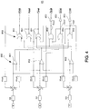
- an inverter-generator apparatus is indicated as a whole by reference numeral 100.
- Such an apparatus 100 is an electronic apparatus configured to transform the energy produced by a generator moved by an internal combustion engine, e.g. available in the form of a three-phase input voltage, to generate a single-phase voltage adapted to supply the loads commonly connected to the normal electrical networks of the residential and industrial systems (machinery, household appliances, lights, electronic apparatuses, etc.).
- such an inverter-generator apparatus 100 comprises a polyphase voltage generator PMG, which supplies at the input a rectifying/control stage 10 configured to rectify and control the polyphase voltage supplied by the polyphase voltage generator PMG to generate a direct output voltage.
- the polyphase voltage generator PMG has a common node N for connecting the phases.
- the apparatus 100 comprises a DC/AC converter stage 40 configured to operate on two direct voltages having equal amplitude.
- a DC/AC converter stage is connected to the rectifying/control stage 10 by means of a first DCB+ and a second DCB- conductive line.
- the DC/AC converter stage 40 comprises an analog/digital control unit CONTR operating on the basis of appropriate software.
- Such a DC/AC converter stage is configured to generate, in response to the direct voltage generated by the rectifying/control stage 10, a first alternating output voltage Vout1 between a first output terminal L1 and a common apparatus terminal GND of the apparatus 100.
- a common terminal GND of the apparatus 100 is connected to the common node N of the polyphase generator PMG.
- the DC/AC converter stage 40 includes a first Half Bridge inverter 41 connected between the first DCB+ and second DCB- conductive lines.
- a first Half Bridge inverter 41 includes first transistors Q1, Q2 which can be activated/deactivated by the control unit CONTR to generate, in response to the direct voltage generated by the rectifying/control stage 10, the aforesaid first output alternating voltage Vout1 between the first output terminal L1 and the common terminal GND of the apparatus.
- the first output voltage Vout1 is generated by means of an appropriate filter LC.
- the apparatus 100 comprises a voltage storage stage 50 interposed between the rectifying/control stage 10 and the DC/AC converter stage 40.
- such a storage stage 50 comprises a first capacitor Ch, connected between the first conductive line DCB+ and the common terminal GND of the apparatus.
- a first capacitor Ch is configured to store a first direct voltage VDC+ of the direct voltage generated by the rectifying/control stage 10.
- the storage stage 50 includes a second capacitor Cl, connected between the second conductive line DCB- and the common terminal GND of the apparatus.
- Such a second capacitor Cl is configured to store a second direct voltage VDC- of the direct voltage generated by the rectifying/control stage 10.
- the first VDC+ and second VDC- direct voltages have the same amplitude and their sum is equal to the aforesaid direct voltage.
- the aforesaid rectifying/control stage 10 includes a first 1 and a distinct second 2 group of mutually equal controlled-trigger semiconductor electronic devices 3.
- each electronic device of the first group is connected to an electronic device of the second group.
- all controlled-trigger semiconductor electronic devices 3 are mutually equal and generally available in commerce in a single standard package.
- the rectifying/control stage 10 includes a first control circuit 60 of the controlled-trigger semiconductor electronic devices 3 of the first group 1.
- a first control circuit 60 is configured to limit a first current circulating in the electronic devices 3 of the first group 1 having a peak value proportional to a first reference voltage Vref1 by timing the activation devices of the semiconductor electronic devices obtained on the basis of phase voltages R, S, T generated by the polyphase voltage generator PMG and of the first direct voltage VDC+.
- the rectifying/control stage 10 includes a second control circuit 70 of the controlled-trigger semiconductor electronic devices 3 of the second group 2.
- a second control circuit 70 is configured to limit a second current circulating in the electronic devices 3 of the second group 2 having a peak value proportional to a second reference voltage Vref2 by timing the activation devices of the semiconductor electronic devices obtained on the basis of the aforesaid phase voltages R, S, T generated by the polyphase voltage generator PMG and of the second direct voltage VDC-.
- the analog/digital control unit CONTR of the DC/AC converter stage 40 is configured to generate the aforesaid first Vref1 and second Vref2 reference voltages to keep the first direct voltage VDC+ stored in the first capacitor Ch and the second direct voltage VDC- stored in the second capacitor Cl equal to predetermined constant values as a load connected to the inverter-generator apparatus as a whole varies.
- the polyphase voltage generator PMG is a three-phase generator which includes a first LR, a second LS and a third LT winding to provide a first R, a second S and a third T phase voltage, to the rectifying/control stage 10, respectively.
- Each winding has a respective first terminal R', S', T' connected to the rectifying/control stage 10 and a second terminal connected to the common node N of the polyphase voltage generator PMG connected to the common terminal GND of the apparatus 100.
- the common terminal GND of the apparatus 100 is connected directly to the terminal to the ground potential EARTH, thus constraining the common node N of the generator PMG to such a potential. This ensures versatility of the inverter-generator apparatus 100 of the invention because it makes it compatible with the safety standards in force in naval and industrial safety standards.
- the common terminal GND of the apparatus 100 is kept disconnected from the ground potential terminal EARTH.
- the DC/AC converter stage 40 of the apparatus 100 further includes a second Half Bridge inverter 42 connected between the first DCB+ and second DCB- conductive lines and similar to the first Half Bridge inverter 41.
- a second Half Bridge inverter 42 includes second transistors Q3, Q4 which can be activated/deactivated by the control unit CONTR to generate, in response to the direct voltage generated by the rectifying/control stage 10, a second output alternating voltage Vout2 between the second output terminal L2 and the common terminal GND of the apparatus.
- the second Half Bridge inverter 42 also includes an output filter LC to provide the second output voltage Vout2.
- the second transistors Q3, Q4 can be activated/deactivated in a manner similar to the first transistors Q1, Q2 and are equal to the latter, the first Vout1 and second Vout2 output voltages have the same amplitude and frequency, but different phase.
- the DC/AC converter stage 40 of the apparatus 100 is configured to generate, in response to the direct voltage generated by the rectifying/control stage 10, a differential output alternating voltage Vod between said first L1 and second L2 output terminals.
- a differential output voltage Vod has the same frequency as said first output voltage Vout1 and an amplitude which is double the amplitude of said first voltage Vout1.
- all the controlled-trigger semiconductor electronic devices 3 of the rectifying/control stage 10 are thyristors or SCRs (silicon controller rectifiers).
- the rectifying/control stage 10 comprises six thyristors 3 as a whole.
- the three thyristors 3 of the first group 1 have a cathode terminal connected to the first conductive line DCB+ and an anode terminal connected to a cathode terminal of one of the three thyristors of the second group 2.
- the three thyristors of the second group 2 have an anode terminal connected to the second conductive line DCB-.
- Each thyristor 3 has a gate which can be activated by a respective activation signal Rpg, Spg, Tpg, Rng, Sng, Tng applied by either the first 60 or second 70 control circuit, respectively.
- the rectifying/control stage 10 is a three-phase full controlled bridge rectifier which works in a manner similar to the two three-phase half-wave controlled rectifiers, each of which allows to control the voltages interdependently on the first Ch and second Cl capacitors, respectively, in order to keep them balanced instant by instant, even with imbalanced and asymmetric loads.
- control unit or controller CONTR comprises a microcontroller (of known type) configured to receive at the input the first VDC+ and second VDC- direct voltages and to provide the first Vref1 and second Vref2 reference voltages to the first 60 and second 70 control circuits, respectively.
- the CONTR cooperates with the first 60 and second 70 control circuits of the three-phase bridge, which are mutually independent to keep the voltages constant on the first Ch and second Cl capacitors.
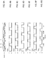
- the waveform of the first phase voltage R differs from a perfect sinusoid (shown in figure with a thin line).
- the first phase voltage R assumes value equal to either the first VDC+ or second VDC- direct voltage of the first Ch and of the second Cl capacitor. This is associated with current pulse waveforms, as shown in figure 5B .
- the zero-crossing position of the first phase voltage R taken in consideration is altered by the switching even if the output voltage of the alternator is kept constant.
- the first 60 and second 70 control circuits of the apparatus 100 of the invention allow to avoid such drawbacks.
- the first control circuit 60 comprises a resettable differential integrator block 61 configured to receive the first/second direct voltage VDC+ at a first input 61a and a first rectified voltage VRadd+ at a second input 61b.
- a rectified voltage VRadd+ is obtained by selecting instant by instant the maximum positive voltage from the phase voltages of the polyphase generator PMG, in particular from the first R, the second S and the third T phase voltage.
- both the first direct voltage VDC+ and the first rectified voltage VRadd+ at the input of the resettable different integrator block 61 are processed with an appropriately scale factor Km.
- Such a resettable integrator block 61 is configured to generated a first integrated voltage Vint+ on an output 61c. In other words, the output of the integrator 61 is equal to the integral of the difference between the greater of the voltages of phases R, S or T and the first voltage VDC+.
- the first control circuit 60 further comprises a comparison block of current references 62 configured to compare the first integrated voltage Vint+ with the first reference voltage Vref1 generated by the control unit CONTR.
- the comparison block 62 is adapted to drive a pulse generator block 63 to generate a first pulse voltage Vpulse +.
- the first control circuit 60 comprises a selection block 64 of the controlled-trigger semiconductor electronic device 3 of the first group 1 to be activated.
- a selection block receives at the input the aforesaid first pulse voltage Vpulse+ and first enabling signals Rmax, Smax, Tmax generated by a voltage discriminator block 65 when the maximum values of the aforesaid phase voltages of the polyphase generator, in particular of the first R, second S and third T phase voltages of the three-phase generator PMG, have been processed.
- the first control circuit 60 comprises a generation block 66 of a reset signal for the resettable differential integrator 61.
- a block 66 is configured to generate the reset signal VRes+ on the basis of:
- the second control circuit 70 comprises a resettable differential integrator block 71 configured to receive the second direct voltage VDC- at a first input 71a and a second rectified voltage VRadd- a second input 71b.
- a second rectified voltage VRadd- is obtained by selecting in each instant the minimum voltage from the phase voltages of the polyphase generator PMG, in particular from the first R, the second S and the third T phase voltage.
- both the second direct voltage VDC- and the second rectified voltage VRadd- at the input of the resettable different integrator block 71 are processed by means of an appropriate scale factor Km.
- the resettable integrator block 71 is configured to generate a second integrated voltage Vint- on a respective output 71c. In other words, the output of the integrator 71 is equal to the integral of the difference between the second voltage VDC- and the smaller of the voltages of the phases R, S or T.
- the second control circuit 70 further comprises a comparison block of current references 72 configured to compare the second integrated voltage Vint-with the second reference voltage Vref2 generated by the control unit CONTR.
- the comparison block 72 is adapted to drive a respective pulse generator block 73 to generate a second pulse voltage Vpulse-.
- the second control circuit 70 further comprises a respective selection block 74 of the controlled-trigger semiconductor electronic device 3 of the second group 2 to be activated.
- a selection block receives at the input the aforesaid second pulse voltage Vpulse- and second enabling signals Rmin, Smin, Tmin generated by a voltage discriminator block 65 when the minimum values of the aforesaid phase voltages of the polyphase generator, in particular of the first R, second S and third T phase voltages of the three-phase generator PMG have been processed.
- the second control circuit 70 comprises a respective generation block 76 of a reset signal for the resettable differential integrator 71.
- a block 76 is configured to generate the reset signal VRes- on the basis of:
- the resettable differential integrator block 61,71 comprises a first differential amplifier 610, 710 having an inverting terminal connected to the first input 61a,71a of the block, a non-inverting terminal connected to the second input 61b,71b of the block and an output terminal connected to a resettable integrator device 611,711.
- the current reference comparison block 62,72 comprises a first comparator 620,720 having an inverting terminal for receiving the first/second reference voltage Vref1/Vref2, a non-inverting terminal for receiving the first/second integrated voltage Vint+/Vint- and an output terminal for driving the pulse generator block 63,73.
- such a pulse generator block 63,73 comprises a flip-flop device 630,730 connected to a time shifting device 631,731.
- the selection block 64,74 comprises three logic gates AND, each configured to receive at the input the first/second pulse voltage Vpulse+/Vpulse- and one of the aforesaid first/second enabling signals Rmax, Smax, Tmax generated by the discriminator block 65.
- the selection block 64,74 is adapted to generate an activation signal Rpg, Spg, Tpg, Rng, Sng, Tng of one of the controlled-trigger semiconductor electronic device 3.
- the reset signal generation block 66,76 comprises:
- Figures 6A-6E show charts exemplifying the voltage signals associated with the diagram of the first control circuit 60 in figure 2 as a function of time. In particular, they show the trends of voltages VDC+, VRaddr+, Vint+, Vref1, VRes+, Vpulse+, in addition to the trend of the first phase voltage R.
- Figures 7A-7E show charts exemplifying the voltage signals associated with the diagram of the second control circuit 70 in figure 3 as a function of time. In particular, they show the trends of voltages VDC-, VRaddr-, Vint-, Vref2, VRes-, Vpulse-, in addition to the trend of the first phase voltage R.
- Figure 8A shows charts exemplifying the first R, the second S and the third T phase voltage signal generated by the three-phase generator PMG of the apparatus 100 as a function of time. Furthermore, figures 8B-8G show charts exemplifying the first/second digital enabling signals Rmax, Smax, Tmax/Rmin, Smin, Tmin generated by the voltage discriminator block 65.
- the differential integrator 61/71 of the first/second control circuit 60/70 is reset by the reset signal generator block 66/76 in two operative conditions:
- the integrator 61/71 exploits the input sinusoidal voltage portion, which is not yet altered by the switching, to obtain the information on the appropriate instant to switch the thyristors 3 of rectifying/control stage 10.
- Vr, Vs and Vt are voltages measured on the first R, second S and third phases T, respectively.
- V int t km ⁇ t 1 t V r t ⁇ V DC + dt where t belongs to the time range [t1,t2] in which the voltage Vr (phase R) is greater than the voltages on phases S and T.
- Vr VDC+ in [t1,t2] because otherwise the differential integrator 61 would be reset by the specific reset block 66.
- the signal of the first integrated voltage Vint+(t) is proportional to the difference between the aforesaid maximum current I LMax and a peak current I Lpeak+ (t) associated with the winding LR.
- the signal of the first integrated voltage Vint+(t) of the equation (4) is compared with the first reference voltage Vref1, in particular with a reference voltage corresponding to a peak current reference signal CONTR, i.e. Vref1(Ipeak+) by means of the current reference comparison block 62.
- the current peak in the first winding LR generated by the thyristor switch 3 of the first group 1 at instant t0 belonging to the interval [t1,t2] in which the identity of the equation (8) is verified, is univocally determined by the reference Vref(Ipeak+) set by the control unit CONTR.
- a pulse Vpulse+ is generated by the pulse generator block 63 having predetermined duration.
- Such a pulse Vpulse+ is sent to the gate of a thyristor 3 of the first group 1 having higher voltage through the selection block 64 by means of one of the digital enabling signals Rmax, Smax, Tmax generated by the discriminator block 65.
- Such a discriminator block 65 comprises, in a comparison section 800, three voltage comparators 801, 802, 803 which are mutually equal, configured to compare the levels of the three input phase voltages R, S, T processed by means of the same scale factor Km.
- the comparison section 800 the first phase voltage R is compared with the second phase voltage S, the second phase voltage S is compared with the third phase voltage T and such a third phase voltage T is compared with the first voltage R.
- a logic state machine 850 determines, instant by instant, which of the three input phases R, S, T has the highest voltage value, generating as a consequence one of the first digital enabling signals Rmax, Smax, Tmax.
- a logic state machine 660 determines, instant by instant, which of the three input phases R, S, T has the lowest voltage value, generating one of the second digital enabling signals Rmax, Smax, Tmax as a consequence.
- the logic state machine 850 comprises three mutually equal logic gates NOR 851 having two inputs and configured to provide the aforesaid first digital enabling signals Rmax, Smax, Tmax at the output.
- the logic state machine 850 comprises three mutually equal logic gates NAND 852 having two inputs and connected at the output to further logic inverter gates 853 to provide the aforesaid second digital enabling signals Rmax, Smax, Tmax available at the output.
- the first digital enabling signals Rmax, Smax, Tmax themselves are used as positive feedback signals of each of the comparators 801, 802, 803 following the processing of such digital signals with appropriate hysteresis constant K hyst .
- further second signals Rmin', Smin', Tmin' of logic value opposite to the aforesaid second digital enabling signals Rmin, Smin, Tmin are used as positive feedback signals of each of the comparators 801, 802, 803. Also in this case, the further second digital signals Rmin', Smin', Tmin' are processed with the aforesaid hysteresis constant K hyst .
- Such a configuration of the discriminator block 65 advantageously allows to avoid spurious switching in case of noise and to impose a predetermined level of the outputs of the comparators 801, 802, 803 in case of minimum differences between the three phase voltages R, S, T.
- the latter condition occurs, for example, if two thyristors 3 of the first group 1 (or two of the second group 2) are both biased, thus constraining the voltage of two of the three phases to the same voltage as the first Ch (or second Cl) capacitor.
- control circuits 60,70 may be immediately extended if the generator PMG has more than three phases, as apparent for a person skilled in the art. This is obtained, in particular, by appropriately modifying the number of input/output signals of the reset block 66,76, of the selection block 64,74 and of the discriminator block 65. Instead, the differential integrator block 61,71, the comparison block 62,72 and the pulse generator block 63,73 remain unchanged.
- the inverter-generator apparatus 100 of the present invention has a simpler circuit structure and is less costly that the inverter-generators of the known type, despite ensuring the same reduced harmonic distortion of the output voltage.
Landscapes
- Engineering & Computer Science (AREA)
- Power Engineering (AREA)
- Control Of Eletrric Generators (AREA)
Claims (16)
- Inverter-Generator-Vorrichtung (100), umfassend:- einen Mehrphasenspannungsgenerator (PMG), welcher einen gemeinsamen Knoten (N) zum Verbinden der Phasen aufweist;- eine zum Gleichrichten und Steuern der durch den Mehrphasenspannungsgenerator (PMG) zugeführten Mehrphasenspannung eingerichtete Gleichrichter-/Steuerstufe (10), welche eine Gleichspannung generiert;- eine DC/AC-Konverter-Stufe (40), welche dazu eingerichtet ist, mit der Gleichspannung zu arbeiten, und mittels einer ersten (DCB+) und einer zweiten (DCB-) Leiterbahn mit der Gleichrichter-/Steuerstufe (10) verbunden ist, wobei die DC/AC-Konverter-Stufe (40) eine Analog-/Digital-Steuereinheit (CONTR) umfasst, wobei die DC/AC-Konverter-Stufe (40) dazu eingerichtet ist, als Reaktion auf die durch die Gleichrichter-/Steuerstufe generierte Gleichspannung eine erste Ausgangswechselspannung (Vout1) zwischen einem ersten Ausgangsanschluss (L1) und einem gemeinsamen Anschluss (GND) der Vorrichtung zu generieren, wobei der gemeinsame Anschluss (GND) mit dem gemeinsamen Knoten (N) des Mehrphasengenerators verbunden ist;- eine Spannungsspeicherstufe (50), welche zwischen der Gleichrichter-/Steuerstufe (10) und der DC/AC-Konverter-Stufe (40) eingefügt ist, wobei die Speicherstufe umfasst:einen ersten Kondensator (Ch), welcher zwischen die erste Leiterbahn (DCB+) und den gemeinsamen Anschluss (GND) der Vorrichtung geschaltet ist und dazu eingerichtet ist, eine erste Gleichspannung (VDC+) der durch die Gleichrichter-/Steuerstufe generierten Gleichspannung zu speichern;einen zweiten Kondensator (CI), welcher zwischen die zweite Leiterbahn (DCB-) und den gemeinsamen Anschluss (GND) der Vorrichtung geschaltet ist und dazu eingerichtet ist, eine zweite Gleichspannung (VDC-) der durch die Gleichrichter-/Steuerstufe generierten Gleichspannung zu speichern;
wobei die erste und die zweite Gleichspannung eine gleiche Amplitude aufweisen,
wobei die Gleichrichter-/Steuerstufe (10) umfasst:- eine erste (1) und eine zweite (2) Gruppe elektronischer Halbleitervorrichtungen (3) mit gegenseitig gleich gesteuertem Trigger, wobei jede elektronische Vorrichtung der ersten Gruppe mit einer elektronischen Vorrichtung der zweiten Gruppe verbunden ist;- eine erste Steuerschaltung (60) der elektronischen Halbleitervorrichtungen (3) mit gesteuertem Trigger der ersten Gruppe (1), wobei die erste Steuerschaltung (60) dazu eingerichtet ist, einen in den elektronischen Vorrichtungen der ersten Gruppe zirkulierenden ersten Strom zu begrenzen, welcher einen zu einer ersten Referenzspannung (Vref1) proportionalen Spitzenwert aufweist, indem die auf der Grundlage von Phasenspannungen (R, S, T), welche durch den Mehrphasenspannungsgenerator (PMG) generiert werden, und der ersten Gleichspannung (VDC+) erhaltenen Aktivierungssteuerungen der elektronischen Halbleitervorrichtungen zeitlich eingestellt werden;- eine zweite Steuerschaltung (70) der elektronischen Halbleitervorrichtungen (3) mit gesteuertem Trigger der zweiten Gruppe (2), wobei die zweite Steuerschaltung (70) dazu eingerichtet ist, einen in den elektronischen Vorrichtungen der zweiten Gruppe zirkulierenden zweiten Strom zu begrenzen, welcher einen zu einer zweiten Referenzspannung (Vref2) proportionalen Spitzenwert aufweist, indem die auf der Grundlage von Phasenspannungen (R, S, T), welche durch den Mehrphasenspannungsgenerator (PMG) generiert werden, und der zweiten Gleichspannung (VDC-) erhaltenen Aktivierungssteuerungen der elektronischen Halbleitervorrichtungen zeitlich eingestellt werden;wobei die Analog-/Digital-Steuereinheit (CONTR) dazu eingerichtet ist, die erste (Vref1) und die zweite (Vref2) Referenzspannung zu generieren, um die erste Gleichspannung (VDC+) in dem ersten Kondensator (Ch) und die zweite Gleichspannung (VDC-) in dem zweiten Kondensator (Cl) gleich vorbestimmten konstanten Werten gespeichert zu halten, wenn eine an die Vorrichtung angeschlossene Last variiert. - Inverter-Generator-Vorrichtung (100) nach Anspruch 1, wobei der Mehrphasenspannungsgenerator (PMG) ein Dreiphasengenerator ist, welcher eine erste (LR), eine zweite (LS) und eine dritte (LT) Windung umfasst, um eine erste (R), eine zweite (S) bzw. eine dritte (T) Phasenspannung bereitzustellen, wobei jede Windung einen ersten Anschluss (R', S', T'), welcher mit der Gleichrichter-/Steuerstufe (10) verbunden ist, und einen zweiten Anschluss aufweist, welcher mit dem gemeinsamen Knoten (N) verbunden ist.
- Inverter-Generator-Vorrichtung (100) nach Anspruch 1 oder 2, wobei die DC/AC-Konverter-Stufe (40) einen ersten Halbbrücken-Inverter (41) umfasst, welcher zwischen die erste (DCB+) und die zweite (DCB-) Leiterbahn geschaltet ist, wobei der erste Halbbrücken-Inverter (41) erste Transistoren (Q1, Q2) umfasst, welche durch die Steuereinheit (CONTR) aktiviert/deaktiviert werden können, um als Reaktion auf die durch die Gleichrichter-/Steuerstufe (10) generierte Gleichspannung die erste Ausgangswechselspannung (Vout1) zwischen dem ersten Ausgangsanschluss (L1) und dem gemeinsamen Anschluss (GND) der Vorrichtung zu generieren.
- Inverter-Generator-Vorrichtung (100) nach dem vorhergehenden Anspruch, wobei die DC/AC-Konverter-Stufe (40) ferner einen zweiten Halbbrücken-Inverter (42) umfasst, welcher zwischen die erste (DCB+) und die zweite (DCB-) Leiterbahn geschaltet ist, und wobei, ähnlich wie der erste Halbbrücken-Inverter (41), der zweite Halbbrücken-Inverter (42) zweite Transistoren (Q3, Q4) umfasst, welche durch die Steuereinheit (CONTR) aktiviert/deaktiviert werden können, um als Reaktion auf die durch die Gleichrichter-/Steuerstufe (10) generierte Gleichspannung eine zweite Ausgangswechselspannung (Vout2) zwischen dem zweiten Ausgangsanschluss (L2) und dem gemeinsamen Anschluss (GND) der Vorrichtung zu generieren, wobei die erste und die zweite Ausgangsspannung die gleiche Amplitude und Frequenz und eine entgegengesetzte Phase aufweisen.
- Inverter-Generator-Vorrichtung (100) nach dem vorhergehenden Anspruch, wobei die ersten Transistoren (Q1, Q2) gleich wie die zweiten Transistoren (Q3, Q4) sind und die DC/AC-Konverter-Stufe (40) dazu eingerichtet ist, als Reaktion auf die durch die Gleichrichter-/Steuerstufe (10) generierte Gleichspannung eine Differenzausgangswechselspannung (Vod) zwischen dem ersten (L1) und dem zweiten (L2) Ausgangsanschluss zu generieren, wobei die Differenzausgangsspannung die gleiche Frequenz wie die erste Ausgangsspannung (Vout1) und eine Amplitude aufweist, welche die doppelte Amplitude der ersten Spannung ist.
- Inverter-Generator-Vorrichtung (100) nach einem der vorhergehenden Ansprüche, wobei die elektronischen Halbleitervorrichtungen (3) mit gesteuertem Trigger der Gleichrichter-/Steuerstufe (10) Thyristoren oder SCRs (silicon controller rectifiers - Siliziumsteuerungsgleichrichter) sind, von welchen jeder ein Gatter aufweist, welches durch ein durch die erste (60) oder die zweite (70) Steuerschaltung angelegtes Aktivierungssignal (Rpg, Spg, Tpg, Rng, Sng, Tng) aktiviert werden kann.
- Inverter-Generator-Vorrichtung (100) nach Anspruch 1, wobei die Steuereinheit (CONTR) einen Mikrocontroller umfasst, welcher dazu eingerichtet ist, an dem Eingang die erste (VDC+) und die zweite (VDC-) Gleichspannung zu empfangen und die erste (Vref1) und die zweite (Vref2) Referenzspannung der ersten (60) bzw. der zweiten (70) Steuerschaltung bereitzustellen.
- Inverter-Generator-Vorrichtung (100) nach Anspruch 1, wobei die erste / die zweite Steuerschaltung (60) / (70) einen rücksetzbaren Differenzintegratorblock (61) / (71) umfasst, welcher dazu eingerichtet ist, an einem ersten Eingang (61a) / (71a) die erste / die zweite Gleichspannung (VDC+) / (VDC-) und an einem zweiten Eingang (61b) / (71b) eine erste / eine zweite gleichgerichtete Spannung (VRadd+) / (VRadd-) zu empfangen, welche aus den Phasenspannungen des Mehrphasengenerators (PMG) durch die maximale / die minimale Phasenspannung repräsentiert ist, und an einem Ausgang (61c) / (71c) eine erste / eine zweite integrierte Spannung (Vint+) / (Vint-) zu generieren.
- Inverter-Generator-Vorrichtung (100) nach Anspruch 8, wobei die erste / die zweite Steuerschaltung (60) / (70) ferner einen Stromreferenzvergleichsblock (62) / (72) umfasst, welcher dazu eingerichtet ist, die erste / die zweite integrierte Spannung (Vint+) / (Vint-) mit der ersten / der zweiten Referenzspannung (Vref1) / (Vref2) zu vergleichen, um einen Impulsgeneratorblock (63) / (73) anzusteuern, welcher dazu geeignet ist, eine erste / eine zweite Impulsspannung (Vpulse+) / (Vpulse-) zu generieren.
- Inverter-Generator-Vorrichtung (100) nach dem vorhergehenden Anspruch, wobei die erste / die zweite Steuerschaltung (60) / (70) ferner einen Auswahlblock (64) / (74) der zu aktivierenden elektronischen Halbleitervorrichtungen (3) mit gesteuertem Trigger der ersten / der zweiten Gruppe (1) / (2) umfasst, wobei der Auswahlblock an dem Eingang die erste / die zweite Impulsspannung (Vpulse+) / (Vpulse-) und erste / zweite Freigabesignale (Rmax, Smax, Tmax) / (Rmin, Smin, Tmin) empfängt, welche durch einen Diskriminatorblock (65) generiert werden, wenn die maximalen / die minimalen Werte der Phasenspannungen des Mehrphasengenerators (PMG) verarbeitet worden sind.
- Inverter-Generator-Vorrichtung (100) nach Anspruch 10, wobei die erste / die zweite Steuerschaltung (60) / (70) einen Generierungsblock (66) / (76) eines Rücksetzsignals für den rücksetzbaren Differenzintegratorblock (61) / (71) umfasst, wobei der Block dazu eingerichtet ist, das Rücksetzsignal (Vres+) / (Vres-) zu generieren auf der Grundlage:- der ersten / der zweiten Gleichspannung (VDC+) / (VDC-), welche einem jeweiligen ersten Eingang (66a) / (76a) des Blocks zugeführt wird;- der ersten / der zweiten gleichgerichteten Spannung (VRadd+) / (VRadd-), welche einem jeweiligen zweiten Eingang (66b) / (76b) des Blocks zugeführt wird;- der ersten / der zweiten Freigabesignale (Rmax, Smax, Tmax) / (Rmin, Smin, Tmin), welche durch den Diskriminatorblock (65) generiert werden, welche einem jeweiligen dritten Eingang (66c) / (76c) des Blocks zugeführt werden.
- Inverter-Generator-Vorrichtung (100) nach Anspruch 8, wobei der rücksetzbare Differenzintegratorblock (61) / (71) einen ersten Differenzverstärker (610) / (710) umfasst, welcher einen invertierenden Anschluss, welcher mit dem ersten Eingang (61a) / (71a) des Blocks verbunden ist, einen nicht invertierenden Anschluss, welcher mit dem zweiten Eingang (61b) / (71b) des Blocks verbunden ist, und einen Ausgangsanschluss aufweist, welcher mit einer rücksetzbaren Integratorvorrichtung (611) / (711) verbunden ist.
- Inverter-Generator-Vorrichtung (100) nach Anspruch 9, wobei der Stromreferenzvergleichsblock (62) / (72) einen ersten Komparator (620) / (720) umfasst, welcher einen invertierenden Anschluss zum Empfangen der ersten / der zweiten Referenzspannung (Vref1) / (Vref2), einen nicht invertierenden Anschluss zum Empfangen der ersten / der zweiten integrierten Spannung (Vint+) / (Vint-) und einen Ausgangsanschluss zum Ansteuern des Impulsgeneratorblocks (63) / (73) aufweist.
- Inverter-Generator-Vorrichtung (100) nach Anspruch 10, wobei der Impulsgeneratorblock (63) / (73) eine Flip-Flop-Vorrichtung (630) / (730) umfasst, welche mit einer Zeitschaltvorrichtung (631) / (731) verbunden ist.
- Inverter-Generator-Vorrichtung (100) nach Anspruch 10, wobei der Auswahlblock (64) / (74) drei UND-Logikgatter umfasst, welche jeweils dazu eingerichtet sind, an dem Eingang die erste / die zweite Impulsspannung (Vpulse+) / (Vpulse-) und eines der ersten / der zweiten Freigabesignale (Rmax, Smax, Tmax) / (Rmin, Smin, Tmin) zu empfangen, welche durch den Diskriminatorblock (65) generiert werden, um ein Aktivierungssignal (Rpg, Spg, Tpg, Rng, Sng, Tng) der elektronischen Halbleitervorrichtung (3) mit gesteuertem Trigger zu generieren.
- Inverter-Generator-Vorrichtung (100) nach Anspruch 11, wobei der Rücksetzsignalgenerierungsblock (66) / (76) umfasst:- einen zweiten Komparator (660) / 760), welcher einen nicht invertierenden Anschluss, welcher mit dem ersten Eingang (66a) / (76a) des Blocks verbunden ist, einen invertierenden Anschluss, welcher mit einem zweiten Eingang (66b) / (76b) des Blocks verbunden ist, und einen Ausgang aufweist, welcher dazu geeignet ist, durch Ansteuern eines ersten Eingangs eines ersten ODER-Logikgatters (661) / (761) ein Rücksetzsignal (Vres+) / (Vres-) zu generieren;- Impulsgenerierungsmodule (662) / (762) an Signalaufwärtsflanken, welche dazu geeignet sind, die ersten / die zweiten Freigabesignale (Rmax, Smax, Tmax) / (Rmin, Smin, Tmin) zu empfangen, welche durch den Diskriminatorblock (65) generiert werden, um mittels eines zweiten ODER-Logikgatters (663) / (763), welches drei Eingänge aufweist, einen zweiten Eingang des ersten ODER-Logikgatters (661) / (761) anzusteuern.
Priority Applications (1)
| Application Number | Priority Date | Filing Date | Title |
|---|---|---|---|
| EP16425119.1A EP3343745B1 (de) | 2016-12-29 | 2016-12-29 | Wechselrichter-generator-vorrichtung |
Applications Claiming Priority (1)
| Application Number | Priority Date | Filing Date | Title |
|---|---|---|---|
| EP16425119.1A EP3343745B1 (de) | 2016-12-29 | 2016-12-29 | Wechselrichter-generator-vorrichtung |
Publications (2)
| Publication Number | Publication Date |
|---|---|
| EP3343745A1 EP3343745A1 (de) | 2018-07-04 |
| EP3343745B1 true EP3343745B1 (de) | 2020-07-15 |
Family
ID=58094103
Family Applications (1)
| Application Number | Title | Priority Date | Filing Date |
|---|---|---|---|
| EP16425119.1A Active EP3343745B1 (de) | 2016-12-29 | 2016-12-29 | Wechselrichter-generator-vorrichtung |
Country Status (1)
| Country | Link |
|---|---|
| EP (1) | EP3343745B1 (de) |
Families Citing this family (2)
| Publication number | Priority date | Publication date | Assignee | Title |
|---|---|---|---|---|
| CN109104097B (zh) * | 2018-08-30 | 2023-11-24 | 全球能源互联网研究院有限公司 | 一种高频变压器运行试验装置 |
| IT202000025114A1 (it) * | 2020-10-23 | 2022-04-23 | Mo S A I C Motion System And Information Control S R L | Convertitore statico di potenza trifase/monofase |
Family Cites Families (4)
| Publication number | Priority date | Publication date | Assignee | Title |
|---|---|---|---|---|
| US5315497A (en) * | 1991-11-07 | 1994-05-24 | Premier Power, Inc. | Symmetrical universal AC-AC power conditioner |
| JPH05292759A (ja) * | 1992-04-13 | 1993-11-05 | Shinko Electric Co Ltd | エンジン式発電装置 |
| US20020024828A1 (en) * | 2000-08-31 | 2002-02-28 | Hidetake Hayashi | Inverter suitable for use with portable AC power supply unit |
| JP4279640B2 (ja) * | 2003-09-26 | 2009-06-17 | 東芝三菱電機産業システム株式会社 | 電力変換装置 |
-
2016
- 2016-12-29 EP EP16425119.1A patent/EP3343745B1/de active Active
Non-Patent Citations (1)
| Title |
|---|
| None * |
Also Published As
| Publication number | Publication date |
|---|---|
| EP3343745A1 (de) | 2018-07-04 |
Similar Documents
| Publication | Publication Date | Title |
|---|---|---|
| US11456679B2 (en) | Voltage level multiplier module for multilevel power converters | |
| US10541598B1 (en) | DC power generating system with voltage ripple compensation | |
| US9871462B2 (en) | Regenerative variable frequency drive with auxiliary power supply | |
| EP0338512B1 (de) | Durch einen Motor angetriebener Generator | |
| EP1921740A2 (de) | Wechselrichtersteuerung | |
| AU2017336112B2 (en) | Control device for power converter | |
| US9899917B2 (en) | Method for producing an output voltage and assembly for performing the method | |
| US9831676B2 (en) | Power conversion device and three-phase AC power supply device | |
| US8995152B2 (en) | Inverter circuit | |
| EP3343745B1 (de) | Wechselrichter-generator-vorrichtung | |
| RU2668416C1 (ru) | Трехуровневый преобразователь частоты | |
| Song et al. | One-Cycle Control of induction machine traction drive for high speed railway part I: Multi-pulse width modulation region | |
| US11165359B2 (en) | Power conversion system configured to perform power conversion between direct current and three-phase alternating current | |
| JP5047210B2 (ja) | 電力変換装置 | |
| JP4693214B2 (ja) | インバータ装置 | |
| JP2020031507A (ja) | 電力変換装置及び、これを用いたインバータ装置 | |
| JP2000139085A (ja) | 電力変換装置 | |
| Gleissner et al. | Operation of fault-tolerant inverters with DC-link midpoint connection for adjustable speed drives | |
| JP2017192207A (ja) | 回転電機システムおよび回転電機システムの制御方法 | |
| Xie et al. | Supply voltage regulation for PMSM-Based ISG system with a shunt voltage source inverter | |
| JP3193809B2 (ja) | 三相整流装置 | |
| JP3177085B2 (ja) | 電力変換装置 | |
| Baazoug et al. | Design of an adaptive feed-forward control scheme for the DC bus voltage control of single phase grid connected converters | |
| JP6591374B2 (ja) | 励磁装置 | |
| EP4344036A1 (de) | Aktive filtervorladung für einen umrichter mit aktiven filterzellen |
Legal Events
| Date | Code | Title | Description |
|---|---|---|---|
| PUAI | Public reference made under article 153(3) epc to a published international application that has entered the european phase |
Free format text: ORIGINAL CODE: 0009012 |
|
| STAA | Information on the status of an ep patent application or granted ep patent |
Free format text: STATUS: THE APPLICATION HAS BEEN PUBLISHED |
|
| AK | Designated contracting states |
Kind code of ref document: A1 Designated state(s): AL AT BE BG CH CY CZ DE DK EE ES FI FR GB GR HR HU IE IS IT LI LT LU LV MC MK MT NL NO PL PT RO RS SE SI SK SM TR |
|
| AX | Request for extension of the european patent |
Extension state: BA ME |
|
| RBV | Designated contracting states (corrected) |
Designated state(s): AL AT BE BG CH CY CZ DE DK EE ES FI FR GB GR HR HU IE IS IT LI LT LU LV MC MK MT NL NO PL PT RO RS SE SI SK SM TR |
|
| STAA | Information on the status of an ep patent application or granted ep patent |
Free format text: STATUS: REQUEST FOR EXAMINATION WAS MADE |
|
| 17P | Request for examination filed |
Effective date: 20180912 |
|
| GRAP | Despatch of communication of intention to grant a patent |
Free format text: ORIGINAL CODE: EPIDOSNIGR1 |
|
| STAA | Information on the status of an ep patent application or granted ep patent |
Free format text: STATUS: GRANT OF PATENT IS INTENDED |
|
| INTG | Intention to grant announced |
Effective date: 20200326 |
|
| GRAS | Grant fee paid |
Free format text: ORIGINAL CODE: EPIDOSNIGR3 |
|
| GRAA | (expected) grant |
Free format text: ORIGINAL CODE: 0009210 |
|
| STAA | Information on the status of an ep patent application or granted ep patent |
Free format text: STATUS: THE PATENT HAS BEEN GRANTED |
|
| AK | Designated contracting states |
Kind code of ref document: B1 Designated state(s): AL AT BE BG CH CY CZ DE DK EE ES FI FR GB GR HR HU IE IS IT LI LT LU LV MC MK MT NL NO PL PT RO RS SE SI SK SM TR |
|
| REG | Reference to a national code |
Ref country code: GB Ref legal event code: FG4D Ref country code: CH Ref legal event code: EP |
|
| REG | Reference to a national code |
Ref country code: IE Ref legal event code: FG4D |
|
| REG | Reference to a national code |
Ref country code: DE Ref legal event code: R096 Ref document number: 602016039903 Country of ref document: DE |
|
| REG | Reference to a national code |
Ref country code: AT Ref legal event code: REF Ref document number: 1292087 Country of ref document: AT Kind code of ref document: T Effective date: 20200815 |
|
| REG | Reference to a national code |
Ref country code: LT Ref legal event code: MG4D |
|
| REG | Reference to a national code |
Ref country code: AT Ref legal event code: MK05 Ref document number: 1292087 Country of ref document: AT Kind code of ref document: T Effective date: 20200715 |
|
| REG | Reference to a national code |
Ref country code: NL Ref legal event code: MP Effective date: 20200715 |
|
| PG25 | Lapsed in a contracting state [announced via postgrant information from national office to epo] |
Ref country code: ES Free format text: LAPSE BECAUSE OF FAILURE TO SUBMIT A TRANSLATION OF THE DESCRIPTION OR TO PAY THE FEE WITHIN THE PRESCRIBED TIME-LIMIT Effective date: 20200715 Ref country code: PT Free format text: LAPSE BECAUSE OF FAILURE TO SUBMIT A TRANSLATION OF THE DESCRIPTION OR TO PAY THE FEE WITHIN THE PRESCRIBED TIME-LIMIT Effective date: 20201116 Ref country code: LT Free format text: LAPSE BECAUSE OF FAILURE TO SUBMIT A TRANSLATION OF THE DESCRIPTION OR TO PAY THE FEE WITHIN THE PRESCRIBED TIME-LIMIT Effective date: 20200715 Ref country code: HR Free format text: LAPSE BECAUSE OF FAILURE TO SUBMIT A TRANSLATION OF THE DESCRIPTION OR TO PAY THE FEE WITHIN THE PRESCRIBED TIME-LIMIT Effective date: 20200715 Ref country code: AT Free format text: LAPSE BECAUSE OF FAILURE TO SUBMIT A TRANSLATION OF THE DESCRIPTION OR TO PAY THE FEE WITHIN THE PRESCRIBED TIME-LIMIT Effective date: 20200715 Ref country code: SE Free format text: LAPSE BECAUSE OF FAILURE TO SUBMIT A TRANSLATION OF THE DESCRIPTION OR TO PAY THE FEE WITHIN THE PRESCRIBED TIME-LIMIT Effective date: 20200715 Ref country code: BG Free format text: LAPSE BECAUSE OF FAILURE TO SUBMIT A TRANSLATION OF THE DESCRIPTION OR TO PAY THE FEE WITHIN THE PRESCRIBED TIME-LIMIT Effective date: 20201015 Ref country code: GR Free format text: LAPSE BECAUSE OF FAILURE TO SUBMIT A TRANSLATION OF THE DESCRIPTION OR TO PAY THE FEE WITHIN THE PRESCRIBED TIME-LIMIT Effective date: 20201016 Ref country code: NO Free format text: LAPSE BECAUSE OF FAILURE TO SUBMIT A TRANSLATION OF THE DESCRIPTION OR TO PAY THE FEE WITHIN THE PRESCRIBED TIME-LIMIT Effective date: 20201015 Ref country code: FI Free format text: LAPSE BECAUSE OF FAILURE TO SUBMIT A TRANSLATION OF THE DESCRIPTION OR TO PAY THE FEE WITHIN THE PRESCRIBED TIME-LIMIT Effective date: 20200715 |
|
| PGFP | Annual fee paid to national office [announced via postgrant information from national office to epo] |
Ref country code: GB Payment date: 20201223 Year of fee payment: 5 |
|
| PG25 | Lapsed in a contracting state [announced via postgrant information from national office to epo] |
Ref country code: IS Free format text: LAPSE BECAUSE OF FAILURE TO SUBMIT A TRANSLATION OF THE DESCRIPTION OR TO PAY THE FEE WITHIN THE PRESCRIBED TIME-LIMIT Effective date: 20201115 Ref country code: RS Free format text: LAPSE BECAUSE OF FAILURE TO SUBMIT A TRANSLATION OF THE DESCRIPTION OR TO PAY THE FEE WITHIN THE PRESCRIBED TIME-LIMIT Effective date: 20200715 Ref country code: LV Free format text: LAPSE BECAUSE OF FAILURE TO SUBMIT A TRANSLATION OF THE DESCRIPTION OR TO PAY THE FEE WITHIN THE PRESCRIBED TIME-LIMIT Effective date: 20200715 Ref country code: PL Free format text: LAPSE BECAUSE OF FAILURE TO SUBMIT A TRANSLATION OF THE DESCRIPTION OR TO PAY THE FEE WITHIN THE PRESCRIBED TIME-LIMIT Effective date: 20200715 |
|
| PG25 | Lapsed in a contracting state [announced via postgrant information from national office to epo] |
Ref country code: NL Free format text: LAPSE BECAUSE OF FAILURE TO SUBMIT A TRANSLATION OF THE DESCRIPTION OR TO PAY THE FEE WITHIN THE PRESCRIBED TIME-LIMIT Effective date: 20200715 |
|
| REG | Reference to a national code |
Ref country code: DE Ref legal event code: R097 Ref document number: 602016039903 Country of ref document: DE |
|
| PG25 | Lapsed in a contracting state [announced via postgrant information from national office to epo] |
Ref country code: EE Free format text: LAPSE BECAUSE OF FAILURE TO SUBMIT A TRANSLATION OF THE DESCRIPTION OR TO PAY THE FEE WITHIN THE PRESCRIBED TIME-LIMIT Effective date: 20200715 Ref country code: RO Free format text: LAPSE BECAUSE OF FAILURE TO SUBMIT A TRANSLATION OF THE DESCRIPTION OR TO PAY THE FEE WITHIN THE PRESCRIBED TIME-LIMIT Effective date: 20200715 Ref country code: SM Free format text: LAPSE BECAUSE OF FAILURE TO SUBMIT A TRANSLATION OF THE DESCRIPTION OR TO PAY THE FEE WITHIN THE PRESCRIBED TIME-LIMIT Effective date: 20200715 Ref country code: CZ Free format text: LAPSE BECAUSE OF FAILURE TO SUBMIT A TRANSLATION OF THE DESCRIPTION OR TO PAY THE FEE WITHIN THE PRESCRIBED TIME-LIMIT Effective date: 20200715 Ref country code: DK Free format text: LAPSE BECAUSE OF FAILURE TO SUBMIT A TRANSLATION OF THE DESCRIPTION OR TO PAY THE FEE WITHIN THE PRESCRIBED TIME-LIMIT Effective date: 20200715 |
|
| PLBE | No opposition filed within time limit |
Free format text: ORIGINAL CODE: 0009261 |
|
| STAA | Information on the status of an ep patent application or granted ep patent |
Free format text: STATUS: NO OPPOSITION FILED WITHIN TIME LIMIT |
|
| PG25 | Lapsed in a contracting state [announced via postgrant information from national office to epo] |
Ref country code: AL Free format text: LAPSE BECAUSE OF FAILURE TO SUBMIT A TRANSLATION OF THE DESCRIPTION OR TO PAY THE FEE WITHIN THE PRESCRIBED TIME-LIMIT Effective date: 20200715 |
|
| 26N | No opposition filed |
Effective date: 20210416 |
|
| PG25 | Lapsed in a contracting state [announced via postgrant information from national office to epo] |
Ref country code: SK Free format text: LAPSE BECAUSE OF FAILURE TO SUBMIT A TRANSLATION OF THE DESCRIPTION OR TO PAY THE FEE WITHIN THE PRESCRIBED TIME-LIMIT Effective date: 20200715 |
|
| REG | Reference to a national code |
Ref country code: DE Ref legal event code: R119 Ref document number: 602016039903 Country of ref document: DE |
|
| REG | Reference to a national code |
Ref country code: CH Ref legal event code: PL |
|
| PG25 | Lapsed in a contracting state [announced via postgrant information from national office to epo] |
Ref country code: SI Free format text: LAPSE BECAUSE OF FAILURE TO SUBMIT A TRANSLATION OF THE DESCRIPTION OR TO PAY THE FEE WITHIN THE PRESCRIBED TIME-LIMIT Effective date: 20200715 Ref country code: MC Free format text: LAPSE BECAUSE OF FAILURE TO SUBMIT A TRANSLATION OF THE DESCRIPTION OR TO PAY THE FEE WITHIN THE PRESCRIBED TIME-LIMIT Effective date: 20200715 |
|
| REG | Reference to a national code |
Ref country code: BE Ref legal event code: MM Effective date: 20201231 |
|
| PG25 | Lapsed in a contracting state [announced via postgrant information from national office to epo] |
Ref country code: IE Free format text: LAPSE BECAUSE OF NON-PAYMENT OF DUE FEES Effective date: 20201229 Ref country code: FR Free format text: LAPSE BECAUSE OF NON-PAYMENT OF DUE FEES Effective date: 20201231 Ref country code: LU Free format text: LAPSE BECAUSE OF NON-PAYMENT OF DUE FEES Effective date: 20201229 |
|
| PG25 | Lapsed in a contracting state [announced via postgrant information from national office to epo] |
Ref country code: LI Free format text: LAPSE BECAUSE OF NON-PAYMENT OF DUE FEES Effective date: 20201231 Ref country code: CH Free format text: LAPSE BECAUSE OF NON-PAYMENT OF DUE FEES Effective date: 20201231 Ref country code: DE Free format text: LAPSE BECAUSE OF NON-PAYMENT OF DUE FEES Effective date: 20210701 |
|
| PG25 | Lapsed in a contracting state [announced via postgrant information from national office to epo] |
Ref country code: TR Free format text: LAPSE BECAUSE OF FAILURE TO SUBMIT A TRANSLATION OF THE DESCRIPTION OR TO PAY THE FEE WITHIN THE PRESCRIBED TIME-LIMIT Effective date: 20200715 Ref country code: MT Free format text: LAPSE BECAUSE OF FAILURE TO SUBMIT A TRANSLATION OF THE DESCRIPTION OR TO PAY THE FEE WITHIN THE PRESCRIBED TIME-LIMIT Effective date: 20200715 Ref country code: CY Free format text: LAPSE BECAUSE OF FAILURE TO SUBMIT A TRANSLATION OF THE DESCRIPTION OR TO PAY THE FEE WITHIN THE PRESCRIBED TIME-LIMIT Effective date: 20200715 |
|
| PG25 | Lapsed in a contracting state [announced via postgrant information from national office to epo] |
Ref country code: MK Free format text: LAPSE BECAUSE OF FAILURE TO SUBMIT A TRANSLATION OF THE DESCRIPTION OR TO PAY THE FEE WITHIN THE PRESCRIBED TIME-LIMIT Effective date: 20200715 |
|
| PG25 | Lapsed in a contracting state [announced via postgrant information from national office to epo] |
Ref country code: BE Free format text: LAPSE BECAUSE OF NON-PAYMENT OF DUE FEES Effective date: 20201231 |
|
| GBPC | Gb: european patent ceased through non-payment of renewal fee |
Effective date: 20211229 |
|
| PG25 | Lapsed in a contracting state [announced via postgrant information from national office to epo] |
Ref country code: GB Free format text: LAPSE BECAUSE OF NON-PAYMENT OF DUE FEES Effective date: 20211229 |
|
| PGFP | Annual fee paid to national office [announced via postgrant information from national office to epo] |
Ref country code: IT Payment date: 20231006 Year of fee payment: 8 |