EP3343644B1 - Light-emitting device and light-emitting device package comprising same - Google Patents
Light-emitting device and light-emitting device package comprising same Download PDFInfo
- Publication number
- EP3343644B1 EP3343644B1 EP16839634.9A EP16839634A EP3343644B1 EP 3343644 B1 EP3343644 B1 EP 3343644B1 EP 16839634 A EP16839634 A EP 16839634A EP 3343644 B1 EP3343644 B1 EP 3343644B1
- Authority
- EP
- European Patent Office
- Prior art keywords
- light
- type semiconductor
- conductivity type
- semiconductor layer
- layer
- Prior art date
- Legal status (The legal status is an assumption and is not a legal conclusion. Google has not performed a legal analysis and makes no representation as to the accuracy of the status listed.)
- Active
Links
Images

Classifications
-
- H—ELECTRICITY
- H10—SEMICONDUCTOR DEVICES; ELECTRIC SOLID-STATE DEVICES NOT OTHERWISE PROVIDED FOR
- H10H—INORGANIC LIGHT-EMITTING SEMICONDUCTOR DEVICES HAVING POTENTIAL BARRIERS
- H10H20/00—Individual inorganic light-emitting semiconductor devices having potential barriers, e.g. light-emitting diodes [LED]
- H10H20/80—Constructional details
- H10H20/83—Electrodes
- H10H20/831—Electrodes characterised by their shape
- H10H20/8312—Electrodes characterised by their shape extending at least partially through the bodies
-
- H—ELECTRICITY
- H10—SEMICONDUCTOR DEVICES; ELECTRIC SOLID-STATE DEVICES NOT OTHERWISE PROVIDED FOR
- H10H—INORGANIC LIGHT-EMITTING SEMICONDUCTOR DEVICES HAVING POTENTIAL BARRIERS
- H10H20/00—Individual inorganic light-emitting semiconductor devices having potential barriers, e.g. light-emitting diodes [LED]
- H10H20/80—Constructional details
- H10H20/81—Bodies
- H10H20/811—Bodies having quantum effect structures or superlattices, e.g. tunnel junctions
- H10H20/812—Bodies having quantum effect structures or superlattices, e.g. tunnel junctions within the light-emitting regions, e.g. having quantum confinement structures
-
- H—ELECTRICITY
- H10—SEMICONDUCTOR DEVICES; ELECTRIC SOLID-STATE DEVICES NOT OTHERWISE PROVIDED FOR
- H10H—INORGANIC LIGHT-EMITTING SEMICONDUCTOR DEVICES HAVING POTENTIAL BARRIERS
- H10H20/00—Individual inorganic light-emitting semiconductor devices having potential barriers, e.g. light-emitting diodes [LED]
- H10H20/80—Constructional details
- H10H20/81—Bodies
- H10H20/815—Bodies having stress relaxation structures, e.g. buffer layers
-
- H—ELECTRICITY
- H10—SEMICONDUCTOR DEVICES; ELECTRIC SOLID-STATE DEVICES NOT OTHERWISE PROVIDED FOR
- H10H—INORGANIC LIGHT-EMITTING SEMICONDUCTOR DEVICES HAVING POTENTIAL BARRIERS
- H10H20/00—Individual inorganic light-emitting semiconductor devices having potential barriers, e.g. light-emitting diodes [LED]
- H10H20/80—Constructional details
- H10H20/81—Bodies
- H10H20/819—Bodies characterised by their shape, e.g. curved or truncated substrates
- H10H20/82—Roughened surfaces, e.g. at the interface between epitaxial layers
-
- H—ELECTRICITY
- H10—SEMICONDUCTOR DEVICES; ELECTRIC SOLID-STATE DEVICES NOT OTHERWISE PROVIDED FOR
- H10H—INORGANIC LIGHT-EMITTING SEMICONDUCTOR DEVICES HAVING POTENTIAL BARRIERS
- H10H20/00—Individual inorganic light-emitting semiconductor devices having potential barriers, e.g. light-emitting diodes [LED]
- H10H20/80—Constructional details
- H10H20/81—Bodies
- H10H20/822—Materials of the light-emitting regions
- H10H20/824—Materials of the light-emitting regions comprising only Group III-V materials, e.g. GaP
- H10H20/825—Materials of the light-emitting regions comprising only Group III-V materials, e.g. GaP containing nitrogen, e.g. GaN
-
- H—ELECTRICITY
- H10—SEMICONDUCTOR DEVICES; ELECTRIC SOLID-STATE DEVICES NOT OTHERWISE PROVIDED FOR
- H10H—INORGANIC LIGHT-EMITTING SEMICONDUCTOR DEVICES HAVING POTENTIAL BARRIERS
- H10H20/00—Individual inorganic light-emitting semiconductor devices having potential barriers, e.g. light-emitting diodes [LED]
- H10H20/80—Constructional details
- H10H20/83—Electrodes
-
- H—ELECTRICITY
- H10—SEMICONDUCTOR DEVICES; ELECTRIC SOLID-STATE DEVICES NOT OTHERWISE PROVIDED FOR
- H10H—INORGANIC LIGHT-EMITTING SEMICONDUCTOR DEVICES HAVING POTENTIAL BARRIERS
- H10H20/00—Individual inorganic light-emitting semiconductor devices having potential barriers, e.g. light-emitting diodes [LED]
- H10H20/80—Constructional details
- H10H20/84—Coatings, e.g. passivation layers or antireflective coatings
-
- H—ELECTRICITY
- H10—SEMICONDUCTOR DEVICES; ELECTRIC SOLID-STATE DEVICES NOT OTHERWISE PROVIDED FOR
- H10H—INORGANIC LIGHT-EMITTING SEMICONDUCTOR DEVICES HAVING POTENTIAL BARRIERS
- H10H20/00—Individual inorganic light-emitting semiconductor devices having potential barriers, e.g. light-emitting diodes [LED]
- H10H20/80—Constructional details
- H10H20/85—Packages
- H10H20/8506—Containers
-
- H—ELECTRICITY
- H10—SEMICONDUCTOR DEVICES; ELECTRIC SOLID-STATE DEVICES NOT OTHERWISE PROVIDED FOR
- H10H—INORGANIC LIGHT-EMITTING SEMICONDUCTOR DEVICES HAVING POTENTIAL BARRIERS
- H10H20/00—Individual inorganic light-emitting semiconductor devices having potential barriers, e.g. light-emitting diodes [LED]
- H10H20/80—Constructional details
- H10H20/85—Packages
- H10H20/857—Interconnections, e.g. lead-frames, bond wires or solder balls
-
- H—ELECTRICITY
- H10—SEMICONDUCTOR DEVICES; ELECTRIC SOLID-STATE DEVICES NOT OTHERWISE PROVIDED FOR
- H10H—INORGANIC LIGHT-EMITTING SEMICONDUCTOR DEVICES HAVING POTENTIAL BARRIERS
- H10H20/00—Individual inorganic light-emitting semiconductor devices having potential barriers, e.g. light-emitting diodes [LED]
- H10H20/80—Constructional details
- H10H20/83—Electrodes
- H10H20/832—Electrodes characterised by their material
- H10H20/833—Transparent materials
-
- H—ELECTRICITY
- H10—SEMICONDUCTOR DEVICES; ELECTRIC SOLID-STATE DEVICES NOT OTHERWISE PROVIDED FOR
- H10H—INORGANIC LIGHT-EMITTING SEMICONDUCTOR DEVICES HAVING POTENTIAL BARRIERS
- H10H20/00—Individual inorganic light-emitting semiconductor devices having potential barriers, e.g. light-emitting diodes [LED]
- H10H20/80—Constructional details
- H10H20/83—Electrodes
- H10H20/832—Electrodes characterised by their material
- H10H20/835—Reflective materials
Definitions
- Embodiments relate to a light-emitting device.
- Group III-V compound semiconductors such as GaN and AlGaN are widely used for optoelectronics, electronic devices and the like, owing to many advantages such as, for example, a wide and easily adjustable band gap energy.
- light-emitting devices such as light-emitting diodes or laser diodes using group III-V or II-VI compound semiconductors may realize various colors of light such as, for example, red, green, and blue light, as well as ultraviolet light, via the development of device materials and thin-film growth technique, and may also realize white light having high luminous efficacy via the use of a fluorescent material or by combining colors.
- These light-emitting devices have advantages of low power consumption, a semi-permanent lifespan, fast response speed, good safety, and eco-friendly properties compared to existing light sources such as, for example, fluorescent lamps and incandescent lamps.
- a light-emitting diode backlight which may substitute for a cold cathode fluorescent lamp (CCFL) constituting a backlight of a liquid crystal display (LCD) apparatus, a white light-emitting diode lighting apparatus, which may substitute for a fluorescent lamp or an incandescent bulb, a vehicle headlight, and a signal lamp.
- CCFL cold cathode fluorescent lamp
- LCD liquid crystal display
- white light-emitting diode lighting apparatus which may substitute for a fluorescent lamp or an incandescent bulb, a vehicle headlight, and a signal lamp.
- EP 2 725 629 A2 discloses a light-emitting devices, which comprises a substrate; a semiconductor laminate placed above the substrate, the semiconductor laminate comprising a second semiconductor layer, an active layer and a first semiconductor layer laminated in this order from the substrate; and a first electrode and a second electrode placed between the substrate and the semiconductor laminate, wherein the semiconductor laminate is divided in a plurality of semiconductor blocks by a groove, wherein the first electrode includes protrusions that are provided in each of the plurality of semiconductor blocks and that penetrate the second semiconductor layer and the active layer to be connected to the first semiconductor layer, and wherein the second electrode is connected to the second semiconductor layer in each of the plurality of semiconductor blocks and has an external connector that is exposed on the bottom of the groove.
- EP 2 725 629 A2 discloses a semiconductor light emitting element in which an electrode is placed between a semiconductor laminate and a substrate.
- US 2014/0034980 A1 and WO 2006/096767 A1 disclose other light-emitting devices with grooves.
- US 2006/0192225 A1 discloses a light emitting device, an encapsulant.
- a light-emitting device is provided with a light-emitting structure, which includes a first conductivity type semiconductor layer, an active layer, and a second conductivity type semiconductor layer, and a first electrode and a second electrode are respectively disposed on the first conductivity type semiconductor layer and the second conductivity type semiconductor layer.
- the light-emitting device emits light having energy determined by the inherent energy band of a constituent material of the active layer in which electrons injected through the first conductivity type semiconductor layer and holes injected through the second conductivity type semiconductor layer meet each other.
- the light emitted from the active layer may be changed depending on the composition of the constituent material of the active layer, and may be blue light, ultraviolet (UV) light, deep-UV light, or the like.
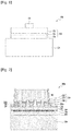
- FIG. 1 is a view illustrating a light-emitting device of the related art.
- a light-emitting structure 120 which includes a first conductivity type semiconductor layer 122, an active layer 124, and a second conductivity type semiconductor layer 126, is disposed on a second electrode 136, and a first electrode 132 is disposed on the first conductivity type semiconductor layer 122.
- the light emitted from the active layer 124 may be absorbed by the first electrode 132, which may deteriorate the efficiency of extraction of light.
- Embodiments provide a light-emitting device having enhanced light extraction efficiency.
- a light-emitting device including a light-emitting structure including a first conductivity type semiconductor layer, a second conductivity type semiconductor layer, and an active layer disposed between the first conductivity type semiconductor layer and the second conductivity type semiconductor layer, and further including a plurality of first recesses configured to penetrate the second conductivity type semiconductor layer and the active layer and be located in a portion of the first conductivity type semiconductor layer, a first electrode electrically connected to the first conductivity type semiconductor layer inside each of the plurality of first recesses, a conductive support substrate electrically connected to the first electrode, a second electrode electrically connected to the second conductivity type semiconductor layer, and an insulating layer disposed between the conductive support substrate and the second conductivity type semiconductor layer, wherein a second recess penetrates the first conductivity type semiconductor layer, the second conductivity type semiconductor layer, and the active layer and is located in a portion of the insulating layer.
- the insulating layer may be disposed so as to extend around the first recesses.
- the second recess includes a light-extractor lower-surface portion configured to form a lower surface of the second recess, a first light-extractor side-surface portion configured to form one side surface of the second recess, and a second light-extractor side-surface portion configured to form a remaining side surface of the second recess.
- the light-extractor lower-surface portion is the insulating layer.
- the light-extractor lower-surface portion is disposed to have a first width for extracting light generated in the active layer.
- the first width is equal to or greater than 3 ⁇ m.
- first light-extractor side-surface portion is disposed to have a first angle with the insulating layer for preventing light generated in the active layer from being again absorbed into the second light-extractor side-surface portion.
- the first angle is equal to or less than 80 degrees.
- a third width of a surface of each first recess may be smaller than a second width of an area in which the first recess is in contact with the first electrode.
- the light-emitting structure may emit light within a UV-B or UV-C wavelength range.
- a composition rate of aluminum (Al) may be equal to or greater than 40%.
- a light-emitting device including a light-emitting structure including a first conductivity type semiconductor layer, a second conductivity type semiconductor layer, and an active layer disposed between the first conductivity type semiconductor layer and the second conductivity type semiconductor layer, and further including a plurality of first recesses configured to penetrate the second conductivity type semiconductor layer and the active layer and be located in a portion of the first conductivity type semiconductor layer, a first electrode electrically connected to the first conductivity type semiconductor layer inside each of the plurality of first recesses, a conductive support substrate electrically connected to the first electrode, a second electrode electrically connected to the second conductivity type semiconductor layer, and an insulating layer disposed between the conductive support substrate and the second conductivity type semiconductor layer, wherein a second recess penetrates the first conductivity type semiconductor layer, the second conductivity type semiconductor layer, and the active layer and is located in a portion of the insulating layer, wherein the second recess includes a light-extractor lower-
- a further embodiment which does not form part of the invention, provides a light-emitting device package including a conductive substrate provided with a cavity, and a light-emitting device disposed so that at least a portion thereof is inserted into the cavity in the conductive substrate, wherein the light-emitting device includes a light-emitting structure including a first conductivity type semiconductor layer, a second conductivity type semiconductor layer, and an active layer disposed between the first conductivity type semiconductor layer and the second conductivity type semiconductor layer, and further including a plurality of first recesses configured to penetrate the second conductivity type semiconductor layer and the active layer and be located in a portion of the first conductivity type semiconductor layer, a first electrode electrically connected to the first conductivity type semiconductor layer inside each of the plurality of first recesses, a conductive support substrate electrically connected to the first electrode, a second electrode electrically connected to the second conductivity type semiconductor layer, and an insulating layer disposed between the conductive support substrate and the second conductivity type semiconductor layer, wherein a second reces
- the second recess may include a light-extractor lower-surface portion configured to form a lower surface of a light extractor, a first light-extractor side-surface portion configured to form one side surface of the light extractor, and a second light-extractor side-surface portion configured to form a remaining side surface of the light extractor.
- the light-extractor lower-surface portion may be the insulating layer.
- the light-extractor lower-surface portion may be disposed to have a first width for extracting light generated in the active layer.
- the first width may be equal to or greater than 3 ⁇ m.
- first light-extractor side-surface portion may be disposed to have a first angle with the insulating layer for preventing light generated in the active layer from being again absorbed into the second light-extractor side-surface portion.
- the first angle may be equal to or less than 80 degrees.
- a composition rate of aluminum (Al) may be equal to or greater than 40%.
- Light-emitting devices include a light exit structure disposed on a first conductivity type semiconductor layer, thereby being capable of increasing the efficiency of extraction of light generated in an active layer, and consequently having enhanced light extraction efficiency.
- Light-emitting devices are vertical light-emitting devices in which a first electrode, which supplies current to a first conductivity type semiconductor layer, is disposed below a light-emitting structure so as to reduce the amount of light that is reflected and discharged upward from the light-emitting structure, and the first electrode may penetrate a second conductivity type semiconductor layer and an active layer to thereby be electrically connected to the first conductivity type semiconductor layer.
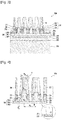
- FIG. 2 is a view illustrating a first embodiment of a light-emitting device , which does not form part of the invention.
- a second conductor layer 236 may be disposed below a light-emitting structure 220, an insulating layer 285 and a first conductor layer 232 may be disposed below the second conductor layer 236, and through-electrodes 233, which extend from the first conductor layer 232, may be in electrical contact with a second conductivity type semiconductor layer 222 in the light-emitting structure 220.
- second electrodes 236a and 236b may be disposed in the edge area of the second conductor layer 236 so as to correspond to the edge of the light-emitting structure 220.
- the light-emitting structure 220 includes a first conductivity type semiconductor layer 222, an active layer 224, and a second conductivity type semiconductor layer 226.
- the first conductivity type semiconductor layer 222 may be formed of group III-V or II-VI compound semiconductors, or the like, and may be doped with a first conductive dopant.
- the first conductivity type semiconductor layer 222 may be formed of a semiconductor material having a composition equation of Al x In y Ga (1-x-y) N (0 ⁇ x ⁇ 1, 0 ⁇ y ⁇ 1, 0 ⁇ x+y ⁇ 1), and for example, may be formed of any one or more of AlGaN, GaN, InAlGaN, AlGaAs, GaP, GaAs, GaAsP, and AlGaInP.
- the first conductive dopant may include an n-type dopant such as Si, Ge, Sn, Se, or Te.
- the first conductivity type semiconductor layer 222 may be formed in a single layer or in multiple layers, without being limited thereto.
- the active layer 224 may be disposed between the first conductivity type semiconductor layer 222 and the second conductivity type semiconductor layer 226, and may include any one of a single well structure, a multi-well structure, a single quantum well structure, a multi-quantum-well structure, a quantum dot structure, and a quantum line structure.
- the active layer 224 may have any one or more pair structures of a well layer and a barrier layer using group III-V compound semiconductors, for example, AlGaN/AlGaN, InGaN/GaN, InGaN/InGaN, AlGaN/GaN, InAlGaN/GaN, GaAs(InGaAs)/AlGaAs, and GaP(InGaP)/AlGaP, without being limited thereto.
- the well layer may be formed of a material, which has a smaller energy band gap than the energy band gap of the barrier layer.
- the second conductivity type semiconductor layer 226 may be formed of a semiconductor compound.
- the second conductivity type semiconductor layer 226 may be formed of, for example, group III-V or II-VI compound semiconductors, and may be doped with a second conductive dopant.
- the second conductivity type semiconductor layer 226 may be formed of a semiconductor material having a composition equation of In x Al y Ga 1-x-y N (0 ⁇ x ⁇ 1, 0 ⁇ y ⁇ 1, 0 ⁇ x+y ⁇ 1), and may be formed of any one or more of AlGaN, GaNAlInN, AlGaAs, GaP, GaAs, GaAsP, and AlGaInP.
- the second conductive dopant may be a p-type dopant such as Mg, Zn, Ca, Sr or Ba.
- the second conductivity type semiconductor layer 226 may be formed in a single layer or in multiple layers, without being limited thereto.
- the light-emitting structure 220 may be grown based on AlGaN, and for example, the composition rate of aluminum (Al) in AlGaN may be 40% or more.
- Al aluminum
- light emission in a TM mode may be increased, compared to a light-emitting device that emits light within a blue wavelength range, so that light is mostly emitted in a vertical direction, which is parallel to the direction of growth of the light-emitting structure 220.
- an electron blocking layer may be disposed between the active layer 224 and the second conductivity type semiconductor layer 226.
- the electron blocking layer may have the structure of a super-lattice.
- the super-lattice may be formed by disposing AlGaN doped with a second conductive dopant and alternately disposing a plurality of GaN layers having different composition rates of aluminum.
- the surface of the first conductivity type semiconductor layer 222 may be uneven to enhance light extraction efficiency, as illustrated.
- the second conductor layer 236 may be disposed below the second conductivity type semiconductor layer 226.
- the second conductor layer 236 may be disposed in surface contact with the second conductivity type semiconductor layer 226, but may not be in contact in the area in which the through-electrodes 233 are formed.
- the edge of the second conductor layer 236 may be disposed further outward than the edge of the second conductivity type semiconductor layer 226, and this serves to secure the area in which the second electrodes 236a and 236b are to be disposed.
- the second conductor layer 236 may be formed of a conductive material, and specifically, may be formed of a metal. More specifically, the second conductor layer may be formed in a single layer or in multiple layers using at least one of silver (Ag), aluminum (Al), titanium (Ti), chrome (Cr), nickel (Ni), copper (Cu), or gold (Au).
- a passivation layer 280 may be formed around the light-emitting structure 220.
- the passivation layer 280 may be formed of an insulating material, and the insulating material may be a non-conductive oxide or nitride.
- the passivation layer 280 may be formed as a silicon oxide (SiO 2 ) layer, an oxide nitride layer, or an oxide aluminum layer.
- the passivation layer 280 which is disposed around the light-emitting structure 220, may also be disposed on the edge of the second conductor layer 236, which is disposed further outward than the edge of the second conductivity type semiconductor layer 226 described above.
- the passivation layer 280 disposed on the edge of the second conductor layer 236 may be opened in the area in which the second electrodes 236a and 236b are formed.
- the first conductor layer 232 may be disposed below the second conductor layer 236 with the insulating layer 285 interposed therebetween.
- the first conductor layer 232 may be formed of a conductive material, and specifically, may be formed of a metal. More specifically, the first conductor layer may be formed in a single layer or in multiple layers using at least one of silver (Ag), aluminum (Al), titanium (Ti), chrome (Cr), nickel (Ni), copper (Cu), or gold (Au).
- the plurality of through-electrodes 233 may be disposed so as to extend upward from the first conductor layer 232.
- the through-electrodes 233 may penetrate the insulating layer 285, the second conductor layer 236, the second conductivity type semiconductor layer 226, and the active layer 224 and may extend to a portion of the first conductivity type semiconductor layer 222 so that the upper surfaces of the through-electrodes 233 may be in surface contact with the first conductivity type semiconductor layer 222.
- Each through-electrode 233 may have a circular or polygonal cross-section.
- the above-described insulating layer 285 may be disposed so as to extend around the through-electrode 233, thereby electrically insulating the through-electrode 233 from the second conductor layer 236, the second conductivity type semiconductor layer 226, and the active layer 224.
- an ohmic layer 240 may be disposed below the first conductor layer 232.
- the ohmic layer may be disposed between the first conductor layer 232 and the first conductivity type semiconductor layer 222, or between the second conductor layer 236 and the second conductivity type semiconductor layer 226.
- the ohmic layer 240 may have a thickness of about 200 ⁇ .
- the ohmic layer 240 may be formed using at least one of indium tin oxide (ITO), indium zinc oxide (IZO), indium zinc tin oxide (IZTO), indium aluminum zinc oxide (IAZO), indium gallium zinc oxide (IGZO), indium gallium tin oxide (IGTO), aluminum zinc oxide (AZO), antimony tin oxide (ATO), gallium zinc oxide (GZO), IZO Nitride (IZON), Al-GaZnO (AGZO), In-GaZnO (IGZO), ZnO, IrOx, RuOx, NiO, RuOx/ITO, Ni/IrOx/Au, Ni/IrOx/Au/ITO, Ag, Ni, Cr, Ti, Al, Rh, Pd, Ir, Sn, In, Ru, Mg, Zn, Pt, Au, or Hf, without being limited to these materials.
- a reflective layer 250 which may act as a reflective electrode, may be disposed below the ohmic layer.
- the reflective layer 250 may be formed as a metal layer using tungsten (W), titanium (Ti), molybdenum (Mo), aluminum (Al), silver (Ag), nickel (Ni), platinum (Pt), rhodium (Rh), or an alloy containing Al, Ag, Pt or Rh.
- W tungsten
- Ti titanium
- Mo molybdenum
- Al aluminum
- silver Ag
- Ni nickel
- Rh rhodium
- Aluminum, silver, or the like may effectively reflect light, which is directed from the active layer 224 downward in FIG. 2 , thereby considerably enhancing the light extraction efficiency of a semiconductor element.
- the width of the reflective layer 250 may be smaller than the width of the ohmic layer 240, and a channel layer 260 may be disposed below the reflective layer 250.
- the width of the channel layer 260 may be greater than the width of the reflective layer 250 so that the channel layer may be disposed so as to surround the reflective layer 250.
- the channel layer 260 may be formed of a conductive material, and for example, may be formed of gold (Au) or tin (Sn).
- a conductive support substrate 270 may be formed of a conductive material such as a metal or a semiconductor material.
- the conductive support substrate may be formed using a metal having excellent electrical conductivity or thermal conductivity, and may be formed using a highly thermally conductive material (e.g. a metal) because it is necessary to sufficiently dissipate heat generated during operation of a semiconductor element.
- the conductive support substrate may be formed of a material selected from among the group consisting of molybdenum (Mo), silicon (Si), tungsten (W), copper (Cu), and aluminum (Al), or an alloy thereof.
- the conductive support substrate may selectively include gold (Au), copper (Cu) alloy, nickel (Ni), copper-tungsten (Cu-W), a carrier wafer (e.g. GaN, Si, Ge, GaAs, ZnO, SiGe, SiC, SiGe, Ga 2 O 3 or the like), or the like.
- Au gold
- Cu copper
- Ni nickel
- Cu-W copper-tungsten
- a carrier wafer e.g. GaN, Si, Ge, GaAs, ZnO, SiGe, SiC, SiGe, Ga 2 O 3 or the like
- the support substrate 270 may be formed to a thickness ranging from 50 ⁇ m to 200 ⁇ m in order to have sufficient mechanical strength for effectively dividing an entire nitride semiconductor into separate chips via a scribing process and a breaking process without bending the semiconductor.
- a bonding layer may bond the channel layer 260 to the conductive support substrate 270, and may be formed of a material selected from the group consisting of gold (Au), tin (Sn), indium (In), aluminum (Al), silicon (Si), silver (Ag), nickel (Ni), and copper (Cu), or an alloy thereof.
- current is uniformly supplied from the first conductor layer 232 to the entire area of the first conductivity type semiconductor layer 222 through the through-electrode 233, and current may be uniformly supplied to the entire area of the second conductivity type semiconductor layer 226, which is in surface contact with the second conductor layer 236.
- the second electrodes 236a and 236b may be disposed on the second conductor layer 236 around the light-emitting structure 220 so that current is uniformly supplied to the entire area of the second conductor layer 236.
- the frequency at which electrons injected through the first conductivity type semiconductor layer 222 and holes injected through the second conductivity type semiconductor layer 226 are combined with each other in the active layer 224 may increase, which may increase the quantity of light discharged from the active layer 224.
- FIG. 3 is a view illustrating another embodiment, which is an embodiment according to the invention, of a light-emitting device.
- the light-emitting device 200b is similar to the embodiment of FIG. 2 , but differs in terms that a first recess penetrates the second conductivity type semiconductor layer 226 and the active layer 224 and is disposed in a portion of the first conductivity type semiconductor layer 222, and a second recess penetrates the first conductivity type semiconductor layer 222, the second conductivity type semiconductor layer 226, and the active layer 224 and is disposed in a portion of the insulating layer 285.
- the first recess may be the edge of each through-electrode, which is formed, from the lower side of the light-emitting structure, in the insulating layer 285, the second conductor layer 236, the second conductivity type semiconductor layer 236, the active layer 224, and a portion of the first conductivity type semiconductor layer 222.
- the through-electrode 233 and the first conductor layer 232 may be formed of the same material.
- the through-electrode 233 and the first conductor layer 232 may form a first electrode.
- first conductor layer 232 may act as a first electrode, and the conductive support substrate 270 may be electrically connected to the first electrode 233.
- the second recess penetrates, from the upper side of the light-emitting structure, the first conductivity type semiconductor layer 222, the active layer 224, and the second conductivity type semiconductor layer 226 so as to expose the insulating layer 285, and acts as a light extractor 286.
- the light extractor 286 may be formed by convex and concave portions of the surface of the first conductivity type semiconductor layer 222.
- the convex portions may be disposed to correspond to the above-described through-electrode 233, and the concave portions may be formed to correspond to the area between the respective through-electrodes 233.
- the concave portions may also be formed in one surface of the insulating layer 285.
- the light extractor 286 includes a light-extractor lower-surface portion 2865, which forms the lower surface of the light extractor 286, a first light-extractor side-surface portion 2861, which forms one side surface of the light extractor 286, and a second light-extractor side-surface portion 2863, which forms the other side surface of the light extractor 286.
- the light-extractor lower-surface portion 2865 is formed of the insulating layer 285.
- the insulating layer 285 that is disposed in the area between the through-electrodes 233 of the light-emitting device 200a according to the embodiment illustrated in FIG. 2 may be disposed so as to be in surface contact with the second conductor layer 236, whereas the insulating layer 285 that is disposed in the area between the through-electrodes 233 of the light-emitting device 200b according to the embodiment illustrated in FIG. 3 is disposed so as to be opened, rather than being in surface contact with the second conductor layer 236.
- Each of the first light-extractor side-surface portion 2861 and the second light-extractor side-surface portion 2863 may include all of the first conductivity type semiconductor layer 222, the active layer 224, and the second conductivity type semiconductor layer 226, and both the first light-extractor side-surface portion 2861 and the second light-extractor side-surface portion 2863 are mesa-etched so that the active layer 224 is opened. Therefore, the light generated in the active layer 224 may be more efficiently extracted to the outside of the light-emitting device 200b, which may increase the light extraction efficiency of the light-emitting device 200b.
- the light generated in the active layer 224 is extracted to the outside of the light-emitting device 200, rather than being absorbed and/or reflected by the first conductivity type semiconductor layer 222, and therefore, the light extraction efficiency of the light-emitting device 200 may be increased.
- the light extractor 286 in the present embodiment is illustrated as being provided in all of the areas between the through-electrodes 233, but this merely illustrates one embodiment.
- the light extractor is not limited to the embodiment illustrated in FIGs. 3 and 4 so long as it can extract the light generated in the active layer 224 to the outside of the light-emitting device 200, and the shape and number of light extractors 286 may be set differently depending on user need and does not limit the scope of the disclosure.
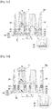
- FIG. 4 is a view illustrating the light-emitting structure of FIG. 3 in detail.
- the light extractor 286 may include no inflection point on the side surface.
- the area C in which the through-electrode 233 is in contact with the first conductivity type semiconductor layer 222 may be provided with a convex portion.
- the convex portion may be formed on the surface of the first conductivity type semiconductor layer 222 so as to correspond to each through-electrode 233, and the concave portion may be formed in the surface of the first conductivity type semiconductor layer 222 so as to correspond to the area between the respective through-electrodes 233.
- the convex and concave portions may also have uneven surfaces B and A.
- a pattern defined by the convex and concave portions of the surface of the first conductivity type semiconductor layer 222 has regularity, but the uneven surfaces of the convex and concave portions may have irregular roughness.
- the width of the convex portion may be greater than the width of the through-electrode 233. More specifically, the third width W 21 of the surface of the through-electrode 233 may be smaller than the second width W 22 of the area in which the through-electrode 233 is in contact with the first conductor layer 232, and the width W 11 of the surface of the convex portion may be greater than the width W 12 of the light-extractor lower surface portion at the height corresponding to the surface of the adjacent concave portion.
- the width W 11 of the surface of the convex portion may be greater than the third width W 21 of the surface of the through-electrode 233, and the width W 12 of the light-extractor lower surface portion at the height corresponding to the surface of the adjacent concave portion may be smaller than the second width W 22 of the area in which the through-electrode 233 is in contact with the first conductor layer 232.
- the width of the light-extractor lower-surface portion 2865 has the first width W 12 required to extract the light generated in the active layer 224.
- the first width W 12 of the light-extractor lower-surface portion 2865 is equal to or greater than 3 ⁇ m.
- the width W 12 of the light-extractor lower-surface portion is below 3 ⁇ m, it is difficult to outwardly extract the light generated in the active layer 224. Therefore, the aforementioned width range may ensure enhanced light extraction efficiency.
- the distance W 3 between the centers of the through-electrodes 233 may range from 50 ⁇ m to 200 ⁇ m.
- the area of the active layer 224 in which light is generated in practice may be reduced, which may cause reduced light extraction efficiency.
- the current spreading characteristics of the first conductivity type semiconductor layer 222 may be reduced, which may cause reduced light extraction efficiency.
- the distance W 3 between the centers of the through-electrodes 233 ranging from 50 ⁇ m to 200 ⁇ m, it is possible to provide the light-emitting device 200 having enhanced light extraction efficiency.
- a first angle between the insulating layer 285, the first light-extractor side-surface portion 2861, and the second light-extractor side-surface portion 2863 is equal to or less than 80 degrees.
- the angle between the insulating layer 285, the first light-extractor side-surface portion 2861, and the second light-extractor side-surface portion 2863 is above 80 degrees, the light extracted through the first light-extractor side-surface portion 2861 may again be absorbed by the second light-extractor side-surface portion 2853, which may reduce light extraction efficiency.
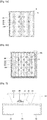
- FIGs. 5a to 5d are views illustrating various embodiments of the light-emitting structure of FIG. 4 .
- the first and second light-extractor side-surface portions 2861 and 2863 of the embodiments may have various shapes.
- first and second light-extractor side-surface portions 2861 and 2863 of the embodiments may include surfaces having roughness.
- the roughness is provided not only on the upper surface of the second conductivity type semiconductor layer, but also on the first and second light-extractor side-surface portions 2861 and 2863, the light emitted from the active layer 224 may be more efficiently extracted.
- first and second light-extractor side-surface portions 2861 and 2863 of the embodiments may have a stepped shape, a concave shape, or a convex shape.
- first and second light-extractor side-surface portions 2861 and 2863 are provided with various shapes, more efficient light extraction of the light-emitting device, and consequently, enhanced light extraction efficiency thereof may be achieved.
- first and second light-extractor side-surface portions 2861 and 2863 may be changed depending on user need, and does not limit the scope of the disclosure.
- FIGs. 6a and 6b are top views of the light-emitting devices of FIGs. 2 and 3 .
- the through-electrodes 233 are disposed below the first conductivity type semiconductor layer 222, and the insulating layer 285 is disposed around each through-electrode 233.
- the through-electrode 233 and the insulating layer 285 are disposed below the first conductivity type semiconductor layer 222, and thus cannot be seen in top views, but are illustrated for convenience of understanding.
- the second electrodes 236a and 236b are disposed outside the passivation layer 280.
- the second electrode 236b disposed in the area "D" may have a width greater than that of the second electrode 236a disposed in the other area, and may be a wire bonding area.
- a concave portion may be located in the area "B" of the surface of the second conductivity type semiconductor layer 222.
- the aforementioned concave portion may be located between the respective through-electrodes 233.
- the through-electrodes 233 which are continuously formed from the first conductor layer 232 to the first conductivity type semiconductor layer 222, are uniformly arranged in the entire area, such that current is uniformly supplied to the entire area of the first conductivity type semiconductor layer 222, and thus the combination of electrons and holes may be efficiently performed in the entire area of the light-emitting structure 220, which may result in enhanced luminous efficacy.
- FIG. 7 is a view illustrating an embodiment of a light-emitting device package.
- the light-emitting device package 300 includes a package body 310, a first electrode part 321, a second electrode part 322, and the light-emitting device 200.
- the package body 310 may have a cavity, and may be formed of an insulating material, and, for example, may be formed of polypthalamide (PPA) resin or a silicon-based material.
- PPA polypthalamide
- Each of the first electrode part 321 and the second electrode part 322 may be disposed on the package body 310 and a portion thereof may be disposed on the bottom surface of the cavity.
- the light-emitting device 200 may be the above-described light-emitting device, and may be disposed on the first electrode part 321 and be electrically connected to the second electrode part 322 via a wire 330.
- a molded part 350 may be disposed around the light-emitting device 200 and the wire 330.
- the molded part 350 may be filled with air, or may be formed of any other protective material.
- the molded part 350 may include phosphors (not illustrated).
- the phosphors may be YAG-based phosphors, nitride-based phosphors, silicate, or mixtures thereof, without being limited thereto.
- a cover 370 may be disposed on top of the package 300.
- the cover 370 may be formed of a light-transmissive material such as glass.
- the light-emitting device may be used in a flip-bonding package.
- a plurality of light-emitting device packages according to the embodiment may be disposed on a substrate to form an array, and optical members, such as a light guide plate, a prism sheet, and a diffusion sheet may be disposed on the optical path of the light-emitting device packages.
- optical members such as a light guide plate, a prism sheet, and a diffusion sheet may be disposed on the optical path of the light-emitting device packages.
- the light-emitting device packages, the substrate, and the optical members may function as a backlight unit.
- a display apparatus, an indicator apparatus, and a lighting apparatus including the light-emitting device package according to the embodiment may be realized.
- the display apparatus may include a bottom cover, a reflector disposed on the bottom cover, a light-emitting module configured to emit light, a light guide plate disposed in front of the reflector to forwardly guide the light emitted from the light-emitting module, optical sheets including prism sheets disposed in front of the light guide plate, a display panel disposed in front of the optical sheets, an image signal output circuit connected to the display panel so as to supply an image signal to the display panel, and a color filter disposed in front of the display panel.
- the bottom cover, the reflector, the light-emitting module, the light guide plate, and the optical sheets may construct a backlight unit.
- the lighting apparatus may include a light source module having a substrate and the light-emitting device package according to the embodiment, a heat radiator configured to dissipate heat from the light source module, and a power supply unit configured to process or convert an electric signal provided from the outside so as to supply the same to the light source module.
- the lighting apparatus may include a lamp, a headlamp, or a street light.
- the head lamp may include a light-emitting module, which includes light-emitting device packages disposed on a substrate, a reflector, which reflects light emitted from the light-emitting module in a given direction, for example, in a forward direction, a lens, which forwardly refracts the light reflected by the reflector, and a shade, which blocks or reflects some of the light, which has been reflected by the reflector and directed to the lens, so as to achieve the light distribution pattern desired by a designer.
- a light-emitting module which includes light-emitting device packages disposed on a substrate
- a reflector which reflects light emitted from the light-emitting module in a given direction, for example, in a forward direction
- a lens which forwardly refracts the light reflected by the reflector
- a shade which blocks or reflects some of the light, which has been reflected by the reflector and directed to the lens, so as to achieve the light distribution pattern desired by a designer
- a light-emitting device which exhibits enhanced light extraction efficiency, may be mounted in a light-emitting device package, and may be realized as a display apparatus, an indicator apparatus, or a lighting apparatus including the light-emitting device package.
Landscapes
- Led Devices (AREA)
- Led Device Packages (AREA)
Applications Claiming Priority (2)
| Application Number | Priority Date | Filing Date | Title |
|---|---|---|---|
| KR1020150120843A KR102378952B1 (ko) | 2015-08-27 | 2015-08-27 | 발광소자 및 이를 포함하는 발광소자 패키지 |
| PCT/KR2016/009444 WO2017034346A1 (ko) | 2015-08-27 | 2016-08-25 | 발광소자 및 이를 포함하는 발광소자 패키지 |
Publications (3)
| Publication Number | Publication Date |
|---|---|
| EP3343644A1 EP3343644A1 (en) | 2018-07-04 |
| EP3343644A4 EP3343644A4 (en) | 2019-04-10 |
| EP3343644B1 true EP3343644B1 (en) | 2021-05-05 |
Family
ID=58100651
Family Applications (1)
| Application Number | Title | Priority Date | Filing Date |
|---|---|---|---|
| EP16839634.9A Active EP3343644B1 (en) | 2015-08-27 | 2016-08-25 | Light-emitting device and light-emitting device package comprising same |
Country Status (6)
Families Citing this family (4)
| Publication number | Priority date | Publication date | Assignee | Title |
|---|---|---|---|---|
| KR102486032B1 (ko) * | 2015-11-04 | 2023-01-11 | 쑤저우 레킨 세미컨덕터 컴퍼니 리미티드 | 발광 소자 및 이를 구비한 조명 장치 |
| JP7096489B2 (ja) * | 2018-09-20 | 2022-07-06 | 日亜化学工業株式会社 | 半導体素子の製造方法 |
| CN113421953B (zh) * | 2021-06-24 | 2022-12-13 | 马鞍山杰生半导体有限公司 | 深紫外发光二极管及其制作方法 |
| JP7440782B2 (ja) * | 2022-01-25 | 2024-02-29 | 日亜化学工業株式会社 | 発光素子の製造方法 |
Family Cites Families (27)
| Publication number | Priority date | Publication date | Assignee | Title |
|---|---|---|---|---|
| US20060192225A1 (en) * | 2005-02-28 | 2006-08-31 | Chua Janet B Y | Light emitting device having a layer of photonic crystals with embedded photoluminescent material and method for fabricating the device |
| US20060204865A1 (en) * | 2005-03-08 | 2006-09-14 | Luminus Devices, Inc. | Patterned light-emitting devices |
| JP2007019099A (ja) * | 2005-07-05 | 2007-01-25 | Sumitomo Electric Ind Ltd | 発光装置およびその製造方法 |
| JP4947954B2 (ja) * | 2005-10-31 | 2012-06-06 | スタンレー電気株式会社 | 発光素子 |
| JP5082504B2 (ja) * | 2006-03-31 | 2012-11-28 | 日亜化学工業株式会社 | 発光素子及び発光素子の製造方法 |
| KR101571577B1 (ko) * | 2008-02-29 | 2015-11-24 | 오스람 옵토 세미컨덕터스 게엠베하 | 모놀리식 광전자 반도체 본체 및 그 제조 방법 |
| US8008683B2 (en) * | 2008-10-22 | 2011-08-30 | Samsung Led Co., Ltd. | Semiconductor light emitting device |
| DE102009006177A1 (de) * | 2008-11-28 | 2010-06-02 | Osram Opto Semiconductors Gmbh | Strahlungsemittierender Halbleiterchip |
| JP5056799B2 (ja) * | 2009-06-24 | 2012-10-24 | 豊田合成株式会社 | Iii族窒化物半導体発光素子およびその製造方法 |
| DE102009034359A1 (de) * | 2009-07-17 | 2011-02-17 | Forschungsverbund Berlin E.V. | P-Kontakt und Leuchtdiode für den ultravioletten Spektralbereich |
| JP5409210B2 (ja) * | 2009-09-01 | 2014-02-05 | 学校法人金沢工業大学 | 半導体発光素子 |
| DE102010024079B4 (de) * | 2010-06-17 | 2025-08-28 | OSRAM Opto Semiconductors Gesellschaft mit beschränkter Haftung | Verfahren zur Herstellung eines optoelektronischen Halbleiterchips und optoelektronischer Halbleiterchip |
| KR101761385B1 (ko) * | 2010-07-12 | 2017-08-04 | 엘지이노텍 주식회사 | 발광 소자 |
| TWI557934B (zh) * | 2010-09-06 | 2016-11-11 | 晶元光電股份有限公司 | 半導體光電元件 |
| KR101663192B1 (ko) * | 2010-10-20 | 2016-10-06 | 엘지이노텍 주식회사 | 발광 소자 |
| KR101873585B1 (ko) * | 2011-08-10 | 2018-07-02 | 엘지이노텍 주식회사 | 발광 소자 패키지 및 이를 구비한 조명 시스템 |
| JP6052962B2 (ja) * | 2012-08-03 | 2016-12-27 | スタンレー電気株式会社 | 半導体発光装置 |
| KR101957816B1 (ko) * | 2012-08-24 | 2019-03-13 | 엘지이노텍 주식회사 | 발광 소자 |
| DE102012108879B4 (de) * | 2012-09-20 | 2024-03-28 | OSRAM Opto Semiconductors Gesellschaft mit beschränkter Haftung | Optoelektronischer Halbleiterchip mit mehreren nebeneinander angeordneten aktiven Bereichen |
| JP5924231B2 (ja) * | 2012-10-24 | 2016-05-25 | 日亜化学工業株式会社 | 半導体発光素子 |
| US9196807B2 (en) * | 2012-10-24 | 2015-11-24 | Nichia Corporation | Light emitting element |
| JP6011244B2 (ja) * | 2012-10-24 | 2016-10-19 | 日亜化学工業株式会社 | 半導体発光素子 |
| JP6210415B2 (ja) * | 2013-07-05 | 2017-10-11 | パナソニックIpマネジメント株式会社 | 紫外線発光素子の製造方法 |
| TWI616004B (zh) * | 2013-11-27 | 2018-02-21 | 晶元光電股份有限公司 | 半導體發光元件 |
| KR20150060405A (ko) * | 2013-11-26 | 2015-06-03 | 서울바이오시스 주식회사 | 복수의 발광셀들을 가지는 발광 다이오드 및 그것을 제조하는 방법 |
| KR102252477B1 (ko) * | 2014-08-05 | 2021-05-17 | 엘지이노텍 주식회사 | 발광소자 및 이를 포함하는 발광소자 패키지 |
| KR102486032B1 (ko) * | 2015-11-04 | 2023-01-11 | 쑤저우 레킨 세미컨덕터 컴퍼니 리미티드 | 발광 소자 및 이를 구비한 조명 장치 |
-
2015
- 2015-08-27 KR KR1020150120843A patent/KR102378952B1/ko active Active
-
2016
- 2016-08-25 WO PCT/KR2016/009444 patent/WO2017034346A1/ko active Application Filing
- 2016-08-25 US US15/749,069 patent/US10263154B2/en active Active
- 2016-08-25 EP EP16839634.9A patent/EP3343644B1/en active Active
- 2016-08-25 CN CN201680049969.5A patent/CN107949920B/zh active Active
- 2016-08-25 JP JP2018504821A patent/JP6878406B2/ja active Active
Also Published As
| Publication number | Publication date |
|---|---|
| WO2017034346A1 (ko) | 2017-03-02 |
| CN107949920A (zh) | 2018-04-20 |
| US20180226542A1 (en) | 2018-08-09 |
| EP3343644A4 (en) | 2019-04-10 |
| CN107949920B (zh) | 2020-11-10 |
| US10263154B2 (en) | 2019-04-16 |
| EP3343644A1 (en) | 2018-07-04 |
| KR20170025035A (ko) | 2017-03-08 |
| JP2018525821A (ja) | 2018-09-06 |
| JP6878406B2 (ja) | 2021-05-26 |
| KR102378952B1 (ko) | 2022-03-25 |
Similar Documents
| Publication | Publication Date | Title |
|---|---|---|
| US11094850B2 (en) | Light emitting device and lighting apparatus having enhanced optical and electrical characteristics by diffusion barrier layer | |
| EP2434545B1 (en) | Light emitting device | |
| US20170025566A1 (en) | Light-emitting element and lighting system | |
| EP3057131B1 (en) | Light-emitting device package and lighting apparatus including the same | |
| KR102175345B1 (ko) | 발광소자 및 조명시스템 | |
| EP2365528A2 (en) | Two light emitting diodes stacked in an n-p-n arrangement and LED package comprising the same | |
| EP3343644B1 (en) | Light-emitting device and light-emitting device package comprising same | |
| KR102163956B1 (ko) | 발광소자 및 조명시스템 | |
| US20180190888A1 (en) | Light-emitting element package and light-emitting element module comprising same | |
| KR102200000B1 (ko) | 발광소자 및 조명시스템 | |
| KR20120019750A (ko) | 발광 소자 | |
| KR102181429B1 (ko) | 발광소자 및 조명시스템 | |
| KR102181404B1 (ko) | 발광소자 및 조명시스템 | |
| KR102153125B1 (ko) | 발광소자 및 조명시스템 | |
| KR102261954B1 (ko) | 형광체 필름, 이를 포함하는 발광 소자 패키지 및 조명 장치 | |
| EP2983215B1 (en) | Light emitting device package | |
| KR102425318B1 (ko) | 발광소자 및 이를 포함하는 발광소자 패키지 | |
| KR102181398B1 (ko) | 발광소자 및 조명시스템 | |
| KR20170082872A (ko) | 발광소자 | |
| KR102163967B1 (ko) | 발광소자 및 조명시스템 | |
| KR102320865B1 (ko) | 발광 소자 | |
| KR20190095749A (ko) | 반도체 소자 패키지 | |
| KR20170022054A (ko) | 발광소자 | |
| KR20170040921A (ko) | 발광 소자 및 이를 구비한 조명 장치 | |
| KR20120136023A (ko) | 발광소자 및 그 발광 소자의 제조 방법 |
Legal Events
| Date | Code | Title | Description |
|---|---|---|---|
| STAA | Information on the status of an ep patent application or granted ep patent |
Free format text: STATUS: THE INTERNATIONAL PUBLICATION HAS BEEN MADE |
|
| PUAI | Public reference made under article 153(3) epc to a published international application that has entered the european phase |
Free format text: ORIGINAL CODE: 0009012 |
|
| STAA | Information on the status of an ep patent application or granted ep patent |
Free format text: STATUS: REQUEST FOR EXAMINATION WAS MADE |
|
| 17P | Request for examination filed |
Effective date: 20180208 |
|
| AK | Designated contracting states |
Kind code of ref document: A1 Designated state(s): AL AT BE BG CH CY CZ DE DK EE ES FI FR GB GR HR HU IE IS IT LI LT LU LV MC MK MT NL NO PL PT RO RS SE SI SK SM TR |
|
| AX | Request for extension of the european patent |
Extension state: BA ME |
|
| DAV | Request for validation of the european patent (deleted) | ||
| DAX | Request for extension of the european patent (deleted) | ||
| A4 | Supplementary search report drawn up and despatched |
Effective date: 20190311 |
|
| RIC1 | Information provided on ipc code assigned before grant |
Ipc: H01L 33/12 20100101ALI20190305BHEP Ipc: H01L 33/26 20100101AFI20190305BHEP Ipc: H01L 33/36 20100101ALI20190305BHEP Ipc: H01L 33/20 20100101ALI20190305BHEP |
|
| STAA | Information on the status of an ep patent application or granted ep patent |
Free format text: STATUS: EXAMINATION IS IN PROGRESS |
|
| 17Q | First examination report despatched |
Effective date: 20200309 |
|
| GRAP | Despatch of communication of intention to grant a patent |
Free format text: ORIGINAL CODE: EPIDOSNIGR1 |
|
| STAA | Information on the status of an ep patent application or granted ep patent |
Free format text: STATUS: GRANT OF PATENT IS INTENDED |
|
| INTG | Intention to grant announced |
Effective date: 20201209 |
|
| GRAS | Grant fee paid |
Free format text: ORIGINAL CODE: EPIDOSNIGR3 |
|
| GRAA | (expected) grant |
Free format text: ORIGINAL CODE: 0009210 |
|
| STAA | Information on the status of an ep patent application or granted ep patent |
Free format text: STATUS: THE PATENT HAS BEEN GRANTED |
|
| AK | Designated contracting states |
Kind code of ref document: B1 Designated state(s): AL AT BE BG CH CY CZ DE DK EE ES FI FR GB GR HR HU IE IS IT LI LT LU LV MC MK MT NL NO PL PT RO RS SE SI SK SM TR |
|
| REG | Reference to a national code |
Ref country code: GB Ref legal event code: FG4D |
|
| REG | Reference to a national code |
Ref country code: CH Ref legal event code: EP |
|
| REG | Reference to a national code |
Ref country code: AT Ref legal event code: REF Ref document number: 1390925 Country of ref document: AT Kind code of ref document: T Effective date: 20210515 |
|
| REG | Reference to a national code |
Ref country code: IE Ref legal event code: FG4D |
|
| REG | Reference to a national code |
Ref country code: DE Ref legal event code: R096 Ref document number: 602016057548 Country of ref document: DE |
|
| RAP2 | Party data changed (patent owner data changed or rights of a patent transferred) |
Owner name: SUZHOU LEKIN SEMICONDUCTOR CO., LTD. |
|
| REG | Reference to a national code |
Ref country code: LT Ref legal event code: MG9D |
|
| REG | Reference to a national code |
Ref country code: DE Ref legal event code: R081 Ref document number: 602016057548 Country of ref document: DE Owner name: SUZHOU LEKIN SEMICONDUCTOR CO. LTD., TAICANG, CN Free format text: FORMER OWNER: LG INNOTEK CO., LTD., SEOUL, KR |
|
| REG | Reference to a national code |
Ref country code: AT Ref legal event code: MK05 Ref document number: 1390925 Country of ref document: AT Kind code of ref document: T Effective date: 20210505 |
|
| PG25 | Lapsed in a contracting state [announced via postgrant information from national office to epo] |
Ref country code: HR Free format text: LAPSE BECAUSE OF FAILURE TO SUBMIT A TRANSLATION OF THE DESCRIPTION OR TO PAY THE FEE WITHIN THE PRESCRIBED TIME-LIMIT Effective date: 20210505 Ref country code: AT Free format text: LAPSE BECAUSE OF FAILURE TO SUBMIT A TRANSLATION OF THE DESCRIPTION OR TO PAY THE FEE WITHIN THE PRESCRIBED TIME-LIMIT Effective date: 20210505 Ref country code: BG Free format text: LAPSE BECAUSE OF FAILURE TO SUBMIT A TRANSLATION OF THE DESCRIPTION OR TO PAY THE FEE WITHIN THE PRESCRIBED TIME-LIMIT Effective date: 20210805 Ref country code: FI Free format text: LAPSE BECAUSE OF FAILURE TO SUBMIT A TRANSLATION OF THE DESCRIPTION OR TO PAY THE FEE WITHIN THE PRESCRIBED TIME-LIMIT Effective date: 20210505 Ref country code: LT Free format text: LAPSE BECAUSE OF FAILURE TO SUBMIT A TRANSLATION OF THE DESCRIPTION OR TO PAY THE FEE WITHIN THE PRESCRIBED TIME-LIMIT Effective date: 20210505 |
|
| PG25 | Lapsed in a contracting state [announced via postgrant information from national office to epo] |
Ref country code: GR Free format text: LAPSE BECAUSE OF FAILURE TO SUBMIT A TRANSLATION OF THE DESCRIPTION OR TO PAY THE FEE WITHIN THE PRESCRIBED TIME-LIMIT Effective date: 20210806 Ref country code: LV Free format text: LAPSE BECAUSE OF FAILURE TO SUBMIT A TRANSLATION OF THE DESCRIPTION OR TO PAY THE FEE WITHIN THE PRESCRIBED TIME-LIMIT Effective date: 20210505 Ref country code: IS Free format text: LAPSE BECAUSE OF FAILURE TO SUBMIT A TRANSLATION OF THE DESCRIPTION OR TO PAY THE FEE WITHIN THE PRESCRIBED TIME-LIMIT Effective date: 20210905 Ref country code: NO Free format text: LAPSE BECAUSE OF FAILURE TO SUBMIT A TRANSLATION OF THE DESCRIPTION OR TO PAY THE FEE WITHIN THE PRESCRIBED TIME-LIMIT Effective date: 20210805 Ref country code: PT Free format text: LAPSE BECAUSE OF FAILURE TO SUBMIT A TRANSLATION OF THE DESCRIPTION OR TO PAY THE FEE WITHIN THE PRESCRIBED TIME-LIMIT Effective date: 20210906 Ref country code: PL Free format text: LAPSE BECAUSE OF FAILURE TO SUBMIT A TRANSLATION OF THE DESCRIPTION OR TO PAY THE FEE WITHIN THE PRESCRIBED TIME-LIMIT Effective date: 20210505 Ref country code: RS Free format text: LAPSE BECAUSE OF FAILURE TO SUBMIT A TRANSLATION OF THE DESCRIPTION OR TO PAY THE FEE WITHIN THE PRESCRIBED TIME-LIMIT Effective date: 20210505 Ref country code: SE Free format text: LAPSE BECAUSE OF FAILURE TO SUBMIT A TRANSLATION OF THE DESCRIPTION OR TO PAY THE FEE WITHIN THE PRESCRIBED TIME-LIMIT Effective date: 20210505 |
|
| REG | Reference to a national code |
Ref country code: NL Ref legal event code: MP Effective date: 20210505 |
|
| PG25 | Lapsed in a contracting state [announced via postgrant information from national office to epo] |
Ref country code: NL Free format text: LAPSE BECAUSE OF FAILURE TO SUBMIT A TRANSLATION OF THE DESCRIPTION OR TO PAY THE FEE WITHIN THE PRESCRIBED TIME-LIMIT Effective date: 20210505 |
|
| PG25 | Lapsed in a contracting state [announced via postgrant information from national office to epo] |
Ref country code: SM Free format text: LAPSE BECAUSE OF FAILURE TO SUBMIT A TRANSLATION OF THE DESCRIPTION OR TO PAY THE FEE WITHIN THE PRESCRIBED TIME-LIMIT Effective date: 20210505 Ref country code: SK Free format text: LAPSE BECAUSE OF FAILURE TO SUBMIT A TRANSLATION OF THE DESCRIPTION OR TO PAY THE FEE WITHIN THE PRESCRIBED TIME-LIMIT Effective date: 20210505 Ref country code: RO Free format text: LAPSE BECAUSE OF FAILURE TO SUBMIT A TRANSLATION OF THE DESCRIPTION OR TO PAY THE FEE WITHIN THE PRESCRIBED TIME-LIMIT Effective date: 20210505 Ref country code: ES Free format text: LAPSE BECAUSE OF FAILURE TO SUBMIT A TRANSLATION OF THE DESCRIPTION OR TO PAY THE FEE WITHIN THE PRESCRIBED TIME-LIMIT Effective date: 20210505 Ref country code: CZ Free format text: LAPSE BECAUSE OF FAILURE TO SUBMIT A TRANSLATION OF THE DESCRIPTION OR TO PAY THE FEE WITHIN THE PRESCRIBED TIME-LIMIT Effective date: 20210505 Ref country code: EE Free format text: LAPSE BECAUSE OF FAILURE TO SUBMIT A TRANSLATION OF THE DESCRIPTION OR TO PAY THE FEE WITHIN THE PRESCRIBED TIME-LIMIT Effective date: 20210505 Ref country code: DK Free format text: LAPSE BECAUSE OF FAILURE TO SUBMIT A TRANSLATION OF THE DESCRIPTION OR TO PAY THE FEE WITHIN THE PRESCRIBED TIME-LIMIT Effective date: 20210505 |
|
| REG | Reference to a national code |
Ref country code: DE Ref legal event code: R097 Ref document number: 602016057548 Country of ref document: DE |
|
| PLBE | No opposition filed within time limit |
Free format text: ORIGINAL CODE: 0009261 |
|
| STAA | Information on the status of an ep patent application or granted ep patent |
Free format text: STATUS: NO OPPOSITION FILED WITHIN TIME LIMIT |
|
| REG | Reference to a national code |
Ref country code: CH Ref legal event code: PL |
|
| PG25 | Lapsed in a contracting state [announced via postgrant information from national office to epo] |
Ref country code: MC Free format text: LAPSE BECAUSE OF FAILURE TO SUBMIT A TRANSLATION OF THE DESCRIPTION OR TO PAY THE FEE WITHIN THE PRESCRIBED TIME-LIMIT Effective date: 20210505 |
|
| 26N | No opposition filed |
Effective date: 20220208 |
|
| REG | Reference to a national code |
Ref country code: BE Ref legal event code: MM Effective date: 20210831 |
|
| GBPC | Gb: european patent ceased through non-payment of renewal fee |
Effective date: 20210825 |
|
| PG25 | Lapsed in a contracting state [announced via postgrant information from national office to epo] |
Ref country code: LI Free format text: LAPSE BECAUSE OF NON-PAYMENT OF DUE FEES Effective date: 20210831 Ref country code: CH Free format text: LAPSE BECAUSE OF NON-PAYMENT OF DUE FEES Effective date: 20210831 |
|
| PG25 | Lapsed in a contracting state [announced via postgrant information from national office to epo] |
Ref country code: IS Free format text: LAPSE BECAUSE OF FAILURE TO SUBMIT A TRANSLATION OF THE DESCRIPTION OR TO PAY THE FEE WITHIN THE PRESCRIBED TIME-LIMIT Effective date: 20210905 Ref country code: LU Free format text: LAPSE BECAUSE OF NON-PAYMENT OF DUE FEES Effective date: 20210825 Ref country code: AL Free format text: LAPSE BECAUSE OF FAILURE TO SUBMIT A TRANSLATION OF THE DESCRIPTION OR TO PAY THE FEE WITHIN THE PRESCRIBED TIME-LIMIT Effective date: 20210505 |
|
| PG25 | Lapsed in a contracting state [announced via postgrant information from national office to epo] |
Ref country code: IT Free format text: LAPSE BECAUSE OF FAILURE TO SUBMIT A TRANSLATION OF THE DESCRIPTION OR TO PAY THE FEE WITHIN THE PRESCRIBED TIME-LIMIT Effective date: 20210505 Ref country code: IE Free format text: LAPSE BECAUSE OF NON-PAYMENT OF DUE FEES Effective date: 20210825 Ref country code: GB Free format text: LAPSE BECAUSE OF NON-PAYMENT OF DUE FEES Effective date: 20210825 Ref country code: FR Free format text: LAPSE BECAUSE OF NON-PAYMENT OF DUE FEES Effective date: 20210831 Ref country code: BE Free format text: LAPSE BECAUSE OF NON-PAYMENT OF DUE FEES Effective date: 20210831 |
|
| PG25 | Lapsed in a contracting state [announced via postgrant information from national office to epo] |
Ref country code: HU Free format text: LAPSE BECAUSE OF FAILURE TO SUBMIT A TRANSLATION OF THE DESCRIPTION OR TO PAY THE FEE WITHIN THE PRESCRIBED TIME-LIMIT; INVALID AB INITIO Effective date: 20160825 |
|
| PG25 | Lapsed in a contracting state [announced via postgrant information from national office to epo] |
Ref country code: CY Free format text: LAPSE BECAUSE OF FAILURE TO SUBMIT A TRANSLATION OF THE DESCRIPTION OR TO PAY THE FEE WITHIN THE PRESCRIBED TIME-LIMIT Effective date: 20210505 |
|
| PG25 | Lapsed in a contracting state [announced via postgrant information from national office to epo] |
Ref country code: MK Free format text: LAPSE BECAUSE OF FAILURE TO SUBMIT A TRANSLATION OF THE DESCRIPTION OR TO PAY THE FEE WITHIN THE PRESCRIBED TIME-LIMIT Effective date: 20210505 |
|
| PG25 | Lapsed in a contracting state [announced via postgrant information from national office to epo] |
Ref country code: TR Free format text: LAPSE BECAUSE OF FAILURE TO SUBMIT A TRANSLATION OF THE DESCRIPTION OR TO PAY THE FEE WITHIN THE PRESCRIBED TIME-LIMIT Effective date: 20210505 |
|
| PG25 | Lapsed in a contracting state [announced via postgrant information from national office to epo] |
Ref country code: MT Free format text: LAPSE BECAUSE OF FAILURE TO SUBMIT A TRANSLATION OF THE DESCRIPTION OR TO PAY THE FEE WITHIN THE PRESCRIBED TIME-LIMIT Effective date: 20210505 |
|
| PGFP | Annual fee paid to national office [announced via postgrant information from national office to epo] |
Ref country code: DE Payment date: 20240709 Year of fee payment: 9 |
|
| REG | Reference to a national code |
Ref country code: DE Ref legal event code: R079 Ref document number: 602016057548 Country of ref document: DE Free format text: PREVIOUS MAIN CLASS: H01L0033260000 Ipc: H10H0020822000 |