EP3343283B1 - Aktives element-array-substrat und anzeigetafel damit - Google Patents
Aktives element-array-substrat und anzeigetafel damit Download PDFInfo
- Publication number
- EP3343283B1 EP3343283B1 EP17200119.0A EP17200119A EP3343283B1 EP 3343283 B1 EP3343283 B1 EP 3343283B1 EP 17200119 A EP17200119 A EP 17200119A EP 3343283 B1 EP3343283 B1 EP 3343283B1
- Authority
- EP
- European Patent Office
- Prior art keywords
- sub
- pixel
- active element
- pixel unit
- electrode
- Prior art date
- Legal status (The legal status is an assumption and is not a legal conclusion. Google has not performed a legal analysis and makes no representation as to the accuracy of the status listed.)
- Active
Links
Images



Classifications
-
- G—PHYSICS
- G02—OPTICS
- G02F—OPTICAL DEVICES OR ARRANGEMENTS FOR THE CONTROL OF LIGHT BY MODIFICATION OF THE OPTICAL PROPERTIES OF THE MEDIA OF THE ELEMENTS INVOLVED THEREIN; NON-LINEAR OPTICS; FREQUENCY-CHANGING OF LIGHT; OPTICAL LOGIC ELEMENTS; OPTICAL ANALOGUE/DIGITAL CONVERTERS
- G02F1/00—Devices or arrangements for the control of the intensity, colour, phase, polarisation or direction of light arriving from an independent light source, e.g. switching, gating or modulating; Non-linear optics
- G02F1/01—Devices or arrangements for the control of the intensity, colour, phase, polarisation or direction of light arriving from an independent light source, e.g. switching, gating or modulating; Non-linear optics for the control of the intensity, phase, polarisation or colour
- G02F1/13—Devices or arrangements for the control of the intensity, colour, phase, polarisation or direction of light arriving from an independent light source, e.g. switching, gating or modulating; Non-linear optics for the control of the intensity, phase, polarisation or colour based on liquid crystals, e.g. single liquid crystal display cells
- G02F1/133—Constructional arrangements; Operation of liquid crystal cells; Circuit arrangements
- G02F1/136—Liquid crystal cells structurally associated with a semi-conducting layer or substrate, e.g. cells forming part of an integrated circuit
- G02F1/1362—Active matrix addressed cells
- G02F1/1368—Active matrix addressed cells in which the switching element is a three-electrode device
-
- G—PHYSICS
- G02—OPTICS
- G02F—OPTICAL DEVICES OR ARRANGEMENTS FOR THE CONTROL OF LIGHT BY MODIFICATION OF THE OPTICAL PROPERTIES OF THE MEDIA OF THE ELEMENTS INVOLVED THEREIN; NON-LINEAR OPTICS; FREQUENCY-CHANGING OF LIGHT; OPTICAL LOGIC ELEMENTS; OPTICAL ANALOGUE/DIGITAL CONVERTERS
- G02F1/00—Devices or arrangements for the control of the intensity, colour, phase, polarisation or direction of light arriving from an independent light source, e.g. switching, gating or modulating; Non-linear optics
- G02F1/01—Devices or arrangements for the control of the intensity, colour, phase, polarisation or direction of light arriving from an independent light source, e.g. switching, gating or modulating; Non-linear optics for the control of the intensity, phase, polarisation or colour
- G02F1/13—Devices or arrangements for the control of the intensity, colour, phase, polarisation or direction of light arriving from an independent light source, e.g. switching, gating or modulating; Non-linear optics for the control of the intensity, phase, polarisation or colour based on liquid crystals, e.g. single liquid crystal display cells
- G02F1/133—Constructional arrangements; Operation of liquid crystal cells; Circuit arrangements
- G02F1/1333—Constructional arrangements; Manufacturing methods
- G02F1/1343—Electrodes
- G02F1/134309—Electrodes characterised by their geometrical arrangement
- G02F1/134336—Matrix
-
- G—PHYSICS
- G02—OPTICS
- G02F—OPTICAL DEVICES OR ARRANGEMENTS FOR THE CONTROL OF LIGHT BY MODIFICATION OF THE OPTICAL PROPERTIES OF THE MEDIA OF THE ELEMENTS INVOLVED THEREIN; NON-LINEAR OPTICS; FREQUENCY-CHANGING OF LIGHT; OPTICAL LOGIC ELEMENTS; OPTICAL ANALOGUE/DIGITAL CONVERTERS
- G02F1/00—Devices or arrangements for the control of the intensity, colour, phase, polarisation or direction of light arriving from an independent light source, e.g. switching, gating or modulating; Non-linear optics
- G02F1/01—Devices or arrangements for the control of the intensity, colour, phase, polarisation or direction of light arriving from an independent light source, e.g. switching, gating or modulating; Non-linear optics for the control of the intensity, phase, polarisation or colour
- G02F1/13—Devices or arrangements for the control of the intensity, colour, phase, polarisation or direction of light arriving from an independent light source, e.g. switching, gating or modulating; Non-linear optics for the control of the intensity, phase, polarisation or colour based on liquid crystals, e.g. single liquid crystal display cells
- G02F1/133—Constructional arrangements; Operation of liquid crystal cells; Circuit arrangements
- G02F1/136—Liquid crystal cells structurally associated with a semi-conducting layer or substrate, e.g. cells forming part of an integrated circuit
- G02F1/1362—Active matrix addressed cells
- G02F1/136286—Wiring, e.g. gate line, drain line
-
- G—PHYSICS
- G02—OPTICS
- G02F—OPTICAL DEVICES OR ARRANGEMENTS FOR THE CONTROL OF LIGHT BY MODIFICATION OF THE OPTICAL PROPERTIES OF THE MEDIA OF THE ELEMENTS INVOLVED THEREIN; NON-LINEAR OPTICS; FREQUENCY-CHANGING OF LIGHT; OPTICAL LOGIC ELEMENTS; OPTICAL ANALOGUE/DIGITAL CONVERTERS
- G02F1/00—Devices or arrangements for the control of the intensity, colour, phase, polarisation or direction of light arriving from an independent light source, e.g. switching, gating or modulating; Non-linear optics
- G02F1/01—Devices or arrangements for the control of the intensity, colour, phase, polarisation or direction of light arriving from an independent light source, e.g. switching, gating or modulating; Non-linear optics for the control of the intensity, phase, polarisation or colour
- G02F1/13—Devices or arrangements for the control of the intensity, colour, phase, polarisation or direction of light arriving from an independent light source, e.g. switching, gating or modulating; Non-linear optics for the control of the intensity, phase, polarisation or colour based on liquid crystals, e.g. single liquid crystal display cells
- G02F1/133—Constructional arrangements; Operation of liquid crystal cells; Circuit arrangements
- G02F1/1333—Constructional arrangements; Manufacturing methods
- G02F1/1337—Surface-induced orientation of the liquid crystal molecules, e.g. by alignment layers
-
- G—PHYSICS
- G02—OPTICS
- G02F—OPTICAL DEVICES OR ARRANGEMENTS FOR THE CONTROL OF LIGHT BY MODIFICATION OF THE OPTICAL PROPERTIES OF THE MEDIA OF THE ELEMENTS INVOLVED THEREIN; NON-LINEAR OPTICS; FREQUENCY-CHANGING OF LIGHT; OPTICAL LOGIC ELEMENTS; OPTICAL ANALOGUE/DIGITAL CONVERTERS
- G02F1/00—Devices or arrangements for the control of the intensity, colour, phase, polarisation or direction of light arriving from an independent light source, e.g. switching, gating or modulating; Non-linear optics
- G02F1/01—Devices or arrangements for the control of the intensity, colour, phase, polarisation or direction of light arriving from an independent light source, e.g. switching, gating or modulating; Non-linear optics for the control of the intensity, phase, polarisation or colour
- G02F1/13—Devices or arrangements for the control of the intensity, colour, phase, polarisation or direction of light arriving from an independent light source, e.g. switching, gating or modulating; Non-linear optics for the control of the intensity, phase, polarisation or colour based on liquid crystals, e.g. single liquid crystal display cells
- G02F1/133—Constructional arrangements; Operation of liquid crystal cells; Circuit arrangements
- G02F1/1333—Constructional arrangements; Manufacturing methods
- G02F1/1339—Gaskets; Spacers; Sealing of cells
-
- G—PHYSICS
- G02—OPTICS
- G02F—OPTICAL DEVICES OR ARRANGEMENTS FOR THE CONTROL OF LIGHT BY MODIFICATION OF THE OPTICAL PROPERTIES OF THE MEDIA OF THE ELEMENTS INVOLVED THEREIN; NON-LINEAR OPTICS; FREQUENCY-CHANGING OF LIGHT; OPTICAL LOGIC ELEMENTS; OPTICAL ANALOGUE/DIGITAL CONVERTERS
- G02F1/00—Devices or arrangements for the control of the intensity, colour, phase, polarisation or direction of light arriving from an independent light source, e.g. switching, gating or modulating; Non-linear optics
- G02F1/01—Devices or arrangements for the control of the intensity, colour, phase, polarisation or direction of light arriving from an independent light source, e.g. switching, gating or modulating; Non-linear optics for the control of the intensity, phase, polarisation or colour
- G02F1/13—Devices or arrangements for the control of the intensity, colour, phase, polarisation or direction of light arriving from an independent light source, e.g. switching, gating or modulating; Non-linear optics for the control of the intensity, phase, polarisation or colour based on liquid crystals, e.g. single liquid crystal display cells
- G02F1/133—Constructional arrangements; Operation of liquid crystal cells; Circuit arrangements
- G02F1/1333—Constructional arrangements; Manufacturing methods
- G02F1/1343—Electrodes
- G02F1/134309—Electrodes characterised by their geometrical arrangement
-
- G—PHYSICS
- G02—OPTICS
- G02F—OPTICAL DEVICES OR ARRANGEMENTS FOR THE CONTROL OF LIGHT BY MODIFICATION OF THE OPTICAL PROPERTIES OF THE MEDIA OF THE ELEMENTS INVOLVED THEREIN; NON-LINEAR OPTICS; FREQUENCY-CHANGING OF LIGHT; OPTICAL LOGIC ELEMENTS; OPTICAL ANALOGUE/DIGITAL CONVERTERS
- G02F1/00—Devices or arrangements for the control of the intensity, colour, phase, polarisation or direction of light arriving from an independent light source, e.g. switching, gating or modulating; Non-linear optics
- G02F1/01—Devices or arrangements for the control of the intensity, colour, phase, polarisation or direction of light arriving from an independent light source, e.g. switching, gating or modulating; Non-linear optics for the control of the intensity, phase, polarisation or colour
- G02F1/13—Devices or arrangements for the control of the intensity, colour, phase, polarisation or direction of light arriving from an independent light source, e.g. switching, gating or modulating; Non-linear optics for the control of the intensity, phase, polarisation or colour based on liquid crystals, e.g. single liquid crystal display cells
- G02F1/133—Constructional arrangements; Operation of liquid crystal cells; Circuit arrangements
- G02F1/136—Liquid crystal cells structurally associated with a semi-conducting layer or substrate, e.g. cells forming part of an integrated circuit
- G02F1/1362—Active matrix addressed cells
-
- G—PHYSICS
- G06—COMPUTING OR CALCULATING; COUNTING
- G06F—ELECTRIC DIGITAL DATA PROCESSING
- G06F3/00—Input arrangements for transferring data to be processed into a form capable of being handled by the computer; Output arrangements for transferring data from processing unit to output unit, e.g. interface arrangements
- G06F3/01—Input arrangements or combined input and output arrangements for interaction between user and computer
- G06F3/03—Arrangements for converting the position or the displacement of a member into a coded form
- G06F3/041—Digitisers, e.g. for touch screens or touch pads, characterised by the transducing means
-
- G—PHYSICS
- G09—EDUCATION; CRYPTOGRAPHY; DISPLAY; ADVERTISING; SEALS
- G09G—ARRANGEMENTS OR CIRCUITS FOR CONTROL OF INDICATING DEVICES USING STATIC MEANS TO PRESENT VARIABLE INFORMATION
- G09G3/00—Control arrangements or circuits, of interest only in connection with visual indicators other than cathode-ray tubes
- G09G3/20—Control arrangements or circuits, of interest only in connection with visual indicators other than cathode-ray tubes for presentation of an assembly of a number of characters, e.g. a page, by composing the assembly by combination of individual elements arranged in a matrix no fixed position being assigned to or needed to be assigned to the individual characters or partial characters
- G09G3/34—Control arrangements or circuits, of interest only in connection with visual indicators other than cathode-ray tubes for presentation of an assembly of a number of characters, e.g. a page, by composing the assembly by combination of individual elements arranged in a matrix no fixed position being assigned to or needed to be assigned to the individual characters or partial characters by control of light from an independent source
- G09G3/36—Control arrangements or circuits, of interest only in connection with visual indicators other than cathode-ray tubes for presentation of an assembly of a number of characters, e.g. a page, by composing the assembly by combination of individual elements arranged in a matrix no fixed position being assigned to or needed to be assigned to the individual characters or partial characters by control of light from an independent source using liquid crystals
-
- H—ELECTRICITY
- H10—SEMICONDUCTOR DEVICES; ELECTRIC SOLID-STATE DEVICES NOT OTHERWISE PROVIDED FOR
- H10D—INORGANIC ELECTRIC SEMICONDUCTOR DEVICES
- H10D84/00—Integrated devices formed in or on semiconductor substrates that comprise only semiconducting layers, e.g. on Si wafers or on GaAs-on-Si wafers
- H10D84/01—Manufacture or treatment
-
- H—ELECTRICITY
- H10—SEMICONDUCTOR DEVICES; ELECTRIC SOLID-STATE DEVICES NOT OTHERWISE PROVIDED FOR
- H10D—INORGANIC ELECTRIC SEMICONDUCTOR DEVICES
- H10D86/00—Integrated devices formed in or on insulating or conducting substrates, e.g. formed in silicon-on-insulator [SOI] substrates or on stainless steel or glass substrates
- H10D86/40—Integrated devices formed in or on insulating or conducting substrates, e.g. formed in silicon-on-insulator [SOI] substrates or on stainless steel or glass substrates characterised by multiple TFTs
- H10D86/441—Interconnections, e.g. scanning lines
-
- H—ELECTRICITY
- H10—SEMICONDUCTOR DEVICES; ELECTRIC SOLID-STATE DEVICES NOT OTHERWISE PROVIDED FOR
- H10D—INORGANIC ELECTRIC SEMICONDUCTOR DEVICES
- H10D86/00—Integrated devices formed in or on insulating or conducting substrates, e.g. formed in silicon-on-insulator [SOI] substrates or on stainless steel or glass substrates
- H10D86/40—Integrated devices formed in or on insulating or conducting substrates, e.g. formed in silicon-on-insulator [SOI] substrates or on stainless steel or glass substrates characterised by multiple TFTs
- H10D86/60—Integrated devices formed in or on insulating or conducting substrates, e.g. formed in silicon-on-insulator [SOI] substrates or on stainless steel or glass substrates characterised by multiple TFTs wherein the TFTs are in active matrices
-
- H—ELECTRICITY
- H10—SEMICONDUCTOR DEVICES; ELECTRIC SOLID-STATE DEVICES NOT OTHERWISE PROVIDED FOR
- H10D—INORGANIC ELECTRIC SEMICONDUCTOR DEVICES
- H10D89/00—Aspects of integrated devices not covered by groups H10D84/00 - H10D88/00
-
- H—ELECTRICITY
- H10—SEMICONDUCTOR DEVICES; ELECTRIC SOLID-STATE DEVICES NOT OTHERWISE PROVIDED FOR
- H10F—INORGANIC SEMICONDUCTOR DEVICES SENSITIVE TO INFRARED RADIATION, LIGHT, ELECTROMAGNETIC RADIATION OF SHORTER WAVELENGTH OR CORPUSCULAR RADIATION
- H10F99/00—Subject matter not provided for in other groups of this subclass
-
- H—ELECTRICITY
- H10—SEMICONDUCTOR DEVICES; ELECTRIC SOLID-STATE DEVICES NOT OTHERWISE PROVIDED FOR
- H10P—GENERIC PROCESSES OR APPARATUS FOR THE MANUFACTURE OR TREATMENT OF DEVICES COVERED BY CLASS H10
- H10P50/00—Etching of wafers, substrates or parts of devices
-
- G—PHYSICS
- G02—OPTICS
- G02F—OPTICAL DEVICES OR ARRANGEMENTS FOR THE CONTROL OF LIGHT BY MODIFICATION OF THE OPTICAL PROPERTIES OF THE MEDIA OF THE ELEMENTS INVOLVED THEREIN; NON-LINEAR OPTICS; FREQUENCY-CHANGING OF LIGHT; OPTICAL LOGIC ELEMENTS; OPTICAL ANALOGUE/DIGITAL CONVERTERS
- G02F1/00—Devices or arrangements for the control of the intensity, colour, phase, polarisation or direction of light arriving from an independent light source, e.g. switching, gating or modulating; Non-linear optics
- G02F1/01—Devices or arrangements for the control of the intensity, colour, phase, polarisation or direction of light arriving from an independent light source, e.g. switching, gating or modulating; Non-linear optics for the control of the intensity, phase, polarisation or colour
- G02F1/13—Devices or arrangements for the control of the intensity, colour, phase, polarisation or direction of light arriving from an independent light source, e.g. switching, gating or modulating; Non-linear optics for the control of the intensity, phase, polarisation or colour based on liquid crystals, e.g. single liquid crystal display cells
- G02F1/133—Constructional arrangements; Operation of liquid crystal cells; Circuit arrangements
- G02F1/1333—Constructional arrangements; Manufacturing methods
- G02F1/1337—Surface-induced orientation of the liquid crystal molecules, e.g. by alignment layers
- G02F1/133707—Structures for producing distorted electric fields, e.g. bumps, protrusions, recesses, slits in pixel electrodes
-
- G—PHYSICS
- G02—OPTICS
- G02F—OPTICAL DEVICES OR ARRANGEMENTS FOR THE CONTROL OF LIGHT BY MODIFICATION OF THE OPTICAL PROPERTIES OF THE MEDIA OF THE ELEMENTS INVOLVED THEREIN; NON-LINEAR OPTICS; FREQUENCY-CHANGING OF LIGHT; OPTICAL LOGIC ELEMENTS; OPTICAL ANALOGUE/DIGITAL CONVERTERS
- G02F1/00—Devices or arrangements for the control of the intensity, colour, phase, polarisation or direction of light arriving from an independent light source, e.g. switching, gating or modulating; Non-linear optics
- G02F1/01—Devices or arrangements for the control of the intensity, colour, phase, polarisation or direction of light arriving from an independent light source, e.g. switching, gating or modulating; Non-linear optics for the control of the intensity, phase, polarisation or colour
- G02F1/13—Devices or arrangements for the control of the intensity, colour, phase, polarisation or direction of light arriving from an independent light source, e.g. switching, gating or modulating; Non-linear optics for the control of the intensity, phase, polarisation or colour based on liquid crystals, e.g. single liquid crystal display cells
- G02F1/133—Constructional arrangements; Operation of liquid crystal cells; Circuit arrangements
- G02F1/1333—Constructional arrangements; Manufacturing methods
- G02F1/1337—Surface-induced orientation of the liquid crystal molecules, e.g. by alignment layers
- G02F1/133711—Surface-induced orientation of the liquid crystal molecules, e.g. by alignment layers by organic films, e.g. polymeric films
-
- G—PHYSICS
- G02—OPTICS
- G02F—OPTICAL DEVICES OR ARRANGEMENTS FOR THE CONTROL OF LIGHT BY MODIFICATION OF THE OPTICAL PROPERTIES OF THE MEDIA OF THE ELEMENTS INVOLVED THEREIN; NON-LINEAR OPTICS; FREQUENCY-CHANGING OF LIGHT; OPTICAL LOGIC ELEMENTS; OPTICAL ANALOGUE/DIGITAL CONVERTERS
- G02F1/00—Devices or arrangements for the control of the intensity, colour, phase, polarisation or direction of light arriving from an independent light source, e.g. switching, gating or modulating; Non-linear optics
- G02F1/01—Devices or arrangements for the control of the intensity, colour, phase, polarisation or direction of light arriving from an independent light source, e.g. switching, gating or modulating; Non-linear optics for the control of the intensity, phase, polarisation or colour
- G02F1/13—Devices or arrangements for the control of the intensity, colour, phase, polarisation or direction of light arriving from an independent light source, e.g. switching, gating or modulating; Non-linear optics for the control of the intensity, phase, polarisation or colour based on liquid crystals, e.g. single liquid crystal display cells
- G02F1/133—Constructional arrangements; Operation of liquid crystal cells; Circuit arrangements
- G02F1/1333—Constructional arrangements; Manufacturing methods
- G02F1/1343—Electrodes
- G02F1/134309—Electrodes characterised by their geometrical arrangement
- G02F1/134345—Subdivided pixels, e.g. for grey scale or redundancy
-
- G—PHYSICS
- G02—OPTICS
- G02F—OPTICAL DEVICES OR ARRANGEMENTS FOR THE CONTROL OF LIGHT BY MODIFICATION OF THE OPTICAL PROPERTIES OF THE MEDIA OF THE ELEMENTS INVOLVED THEREIN; NON-LINEAR OPTICS; FREQUENCY-CHANGING OF LIGHT; OPTICAL LOGIC ELEMENTS; OPTICAL ANALOGUE/DIGITAL CONVERTERS
- G02F1/00—Devices or arrangements for the control of the intensity, colour, phase, polarisation or direction of light arriving from an independent light source, e.g. switching, gating or modulating; Non-linear optics
- G02F1/01—Devices or arrangements for the control of the intensity, colour, phase, polarisation or direction of light arriving from an independent light source, e.g. switching, gating or modulating; Non-linear optics for the control of the intensity, phase, polarisation or colour
- G02F1/13—Devices or arrangements for the control of the intensity, colour, phase, polarisation or direction of light arriving from an independent light source, e.g. switching, gating or modulating; Non-linear optics for the control of the intensity, phase, polarisation or colour based on liquid crystals, e.g. single liquid crystal display cells
- G02F1/133—Constructional arrangements; Operation of liquid crystal cells; Circuit arrangements
- G02F1/136—Liquid crystal cells structurally associated with a semi-conducting layer or substrate, e.g. cells forming part of an integrated circuit
- G02F1/1362—Active matrix addressed cells
- G02F1/136209—Light shielding layers, e.g. black matrix, incorporated in the active matrix substrate, e.g. structurally associated with the switching element
-
- G—PHYSICS
- G02—OPTICS
- G02F—OPTICAL DEVICES OR ARRANGEMENTS FOR THE CONTROL OF LIGHT BY MODIFICATION OF THE OPTICAL PROPERTIES OF THE MEDIA OF THE ELEMENTS INVOLVED THEREIN; NON-LINEAR OPTICS; FREQUENCY-CHANGING OF LIGHT; OPTICAL LOGIC ELEMENTS; OPTICAL ANALOGUE/DIGITAL CONVERTERS
- G02F1/00—Devices or arrangements for the control of the intensity, colour, phase, polarisation or direction of light arriving from an independent light source, e.g. switching, gating or modulating; Non-linear optics
- G02F1/01—Devices or arrangements for the control of the intensity, colour, phase, polarisation or direction of light arriving from an independent light source, e.g. switching, gating or modulating; Non-linear optics for the control of the intensity, phase, polarisation or colour
- G02F1/13—Devices or arrangements for the control of the intensity, colour, phase, polarisation or direction of light arriving from an independent light source, e.g. switching, gating or modulating; Non-linear optics for the control of the intensity, phase, polarisation or colour based on liquid crystals, e.g. single liquid crystal display cells
- G02F1/133—Constructional arrangements; Operation of liquid crystal cells; Circuit arrangements
- G02F1/136—Liquid crystal cells structurally associated with a semi-conducting layer or substrate, e.g. cells forming part of an integrated circuit
- G02F1/1362—Active matrix addressed cells
- G02F1/136213—Storage capacitors associated with the pixel electrode
-
- G—PHYSICS
- G02—OPTICS
- G02F—OPTICAL DEVICES OR ARRANGEMENTS FOR THE CONTROL OF LIGHT BY MODIFICATION OF THE OPTICAL PROPERTIES OF THE MEDIA OF THE ELEMENTS INVOLVED THEREIN; NON-LINEAR OPTICS; FREQUENCY-CHANGING OF LIGHT; OPTICAL LOGIC ELEMENTS; OPTICAL ANALOGUE/DIGITAL CONVERTERS
- G02F1/00—Devices or arrangements for the control of the intensity, colour, phase, polarisation or direction of light arriving from an independent light source, e.g. switching, gating or modulating; Non-linear optics
- G02F1/01—Devices or arrangements for the control of the intensity, colour, phase, polarisation or direction of light arriving from an independent light source, e.g. switching, gating or modulating; Non-linear optics for the control of the intensity, phase, polarisation or colour
- G02F1/13—Devices or arrangements for the control of the intensity, colour, phase, polarisation or direction of light arriving from an independent light source, e.g. switching, gating or modulating; Non-linear optics for the control of the intensity, phase, polarisation or colour based on liquid crystals, e.g. single liquid crystal display cells
- G02F1/133—Constructional arrangements; Operation of liquid crystal cells; Circuit arrangements
- G02F1/136—Liquid crystal cells structurally associated with a semi-conducting layer or substrate, e.g. cells forming part of an integrated circuit
- G02F1/1362—Active matrix addressed cells
- G02F1/136222—Colour filters incorporated in the active matrix substrate
-
- G—PHYSICS
- G09—EDUCATION; CRYPTOGRAPHY; DISPLAY; ADVERTISING; SEALS
- G09G—ARRANGEMENTS OR CIRCUITS FOR CONTROL OF INDICATING DEVICES USING STATIC MEANS TO PRESENT VARIABLE INFORMATION
- G09G2300/00—Aspects of the constitution of display devices
- G09G2300/04—Structural and physical details of display devices
- G09G2300/0421—Structural details of the set of electrodes
- G09G2300/0426—Layout of electrodes and connections
Definitions
- the present invention relates to an active element array substrate and a curved display panel using the same.
- liquid crystal display apparatuses have been widely applied in various electronic devices.
- preset positions of upper and lower substrates need to be adhered to form each pixel.
- the upper and lower substrates are easily dislocated.
- a curved liquid crystal display apparatus As an example, generally, a display apparatus is first formed into a flat structure, and then the liquid crystal display apparatus in the flat structure is bent to obtain the curved liquid crystal display apparatus.
- the liquid crystal display apparatus in the flat structure is greatly bent, because substrates are greatly moved relative to each other, consequently, preset corresponding positions, on a bent part, of the substrates are dislocated, and a phenomenon of disordered liquid crystal arrangement occurs in a dislocated part, and consequently, visual effects are affected.
- the US 2016/306202 A1 , the CN 105 116 654 A and the US 2007/030233 A1 each describe a pixel array for a display having a substrate, at least three different data lines, at least two scan lines and at least three sub-pixels.
- pixel array comprises a common electrode line.
- the second scan line is not located between the second and the third sub-pixel.
- the second sub-pixel and the third sub-pixel are connected to different scan lines.
- the three sub-pixels are located at the same side of the scan line.
- the embodiments of the present invention provide an active element array substrate and a curved display panel using the same.
- a long edge of a sub-pixel is designed to be parallel to an extension direction of the curvature of the curved display panel, so that a region in which liquid crystal arrangement is disordered because upper and lower substrates are dislocated is reduced.
- a first sub-pixel unit, a second sub-pixel unit, and a third sub-pixel unit are supplied by means of a same gate signal and different data signals, so that the first sub-pixel unit, the second sub-pixel unit, and the third sub-pixel unit have respective operating voltages, and present respective expected brightnesses.
- This practice may improve power supply time of each sub-pixel unit to ensure that an active element in each sub-pixel unit is sufficiently charged.
- an active element array substrate of a curved liquid crystal panel comprises a substrate, at least one first data line, at least one second data line, at least one third data line, a plurality of first scan lines, at least one second scan line, at least one common electrode line, at least one first sub-pixel unit, at least one second sub-pixel unit, and at least one third sub-pixel unit.
- the substrate comprises an active region and a peripheral region provided on at least one side of the active region.
- the first data line, the second data line, and the third data line extend along a first direction and are provided on the substrate.
- the first scan lines extend along a second direction and are provided on the substrate, wherein the first direction is not parallel to the second direction; the first data line and the third data line respectively intersect with first and second adjacent ones of the first scan lines to define at least one pixel region in the active region on the substrate.
- the second data line is located between the first data line and the third data line and passes through the pixel region.
- the second scan line and the common electrode line extend along the second direction and are provided on the substrate, wherein the first data line intersects with the second scan line and the common electrode line to define a first sub-pixel region, a second sub-pixel region, and a third sub-pixel region in the pixel region.
- the first sub-pixel unit is provided in the first sub-pixel region and electrically connected to the first data line and the first one of the first scan lines.
- the second sub-pixel unit is provided in the second sub-pixel region and electrically connected to the second data line and the second scan line.
- the third sub-pixel unit is provided in the third sub-pixel region and electrically connected to the third data line and the second scan line.
- a curved display pane comprises the foregoing active element array substrate, an opposite substrate, a liquid crystal layer, and two vertical alignment layers.
- the liquid crystal layer is provided between the active element array substrate and the opposite substrate.
- the vertical alignment layers are respectively provided between the liquid crystal layer and the active element array substrate and between the liquid crystal layer and the opposite substrate.
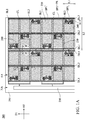
- FIG. 1A is a schematic top view of an active element array substrate 200 according to an embodiment of the present invention.
- the active element array substrate 200 comprises a substrate 210, which comprises an active region AA and a peripheral region NA provided on at least one side of the active region AA.
- the active element array substrate 200 comprises at least one first data line DL1, at least one second data line DL2, at least one third data line DL3, a plurality of first scan lines SL1, at least one second scan lines SL2, at least one common electrode line CL, at least one first sub-pixel unit 220, at least one second sub-pixel unit 230, and at least one third sub-pixel unit 240 that are provided on the substrate 210.
- the first data line DL1, the second data line DL2, and the third data line DL3 extend along a first direction D1 and are sequentially arranged, so that the second data line DL2 is provided between the first data line DL1 and the third data line DL3.
- the first scan lines SL1, the common electrode line CL, and the second scan line SL2 extend along a second direction D2 and are sequentially arranged, so that the common electrode line CL is provided between the first scan lines SL1 and the second scan line SL2.
- the first direction D1 is not parallel to the second direction D2.
- every adjacent two scan lines SL1 respectively intersect with the first data line DL1 and the third data line DL3 to define a pixel region PR in the active region AA on the substrate 210.
- the second data line DL2 passes through the pixel region PR.
- a plurality of pixel regions PR arranged in an array is provided on the substrate 210.
- the pixel region PR is formed by adjacent two first scan lines SL1, one first data line DL1, and one third data line DL3 intersecting with each other.
- the foregoing common electrode line CL intersects with the first data line DL1 and the third data line DL3, and one first scan line SL1, the first data line DL1, and the third data line DL3 in the pixel region PR and the common electrode line CL define a first sub-pixel region SP1 in the pixel region PR.
- the second scan line SL2 intersects with the first data line DL1 and the third data line DL3, and the first data line DL1, the third data line DL3, the common electrode line CL, and the second scan line SL2 define a second sub-pixel region SP2 in the pixel region PR. Then, the other first scan line SL1, the first data line DL1, and the third data line DL3 in the pixel region PR and the second scan line SL2 define a third sub-pixel region SP3 in the pixel region PR.
- the first sub-pixel unit 220 is provided in the first sub-pixel region SP1 and electrically connected to the first data line DL1 and one of the first scan lines SL1.
- the second sub-pixel unit 230 is provided in the second sub-pixel region SP2 and electrically connected to the second data line DL2 and the second scan line SL2.
- the third sub-pixel unit 240 is provided in the third sub-pixel region SP3 and electrically connected to the third data line DL3 and the second scan line SL2.
- the active element array substrate 200 further comprises a gate driver 250, located in the peripheral region NA of the substrate 210.
- the data driver 250 may be a drive chip.
- the gate driver 250 may also be a suitable drive circuit.
- the gate driver 250 comprises at least one pin, wherein the first scan lines SL1 in a same pixel region PR and the second scan line SL2 are electrically connected to a same pin.
- the first sub-pixel unit 220, the second sub-pixel unit 230, and the third sub-pixel unit 240 may be supplied with respective operating voltages at the same time by means of a same gate signal and different data signals (the first data line DL1, the second data line DL2, and the third data line DL3) to present expected brightnesses.
- the present implementation manner controls each sub-pixel unit in a same pixel unit to operate by using one gate line in cooperation with a plurality of data lines, and therefore a quantity of pins needed by the gate driver 250 can be further reduced, and because the quantity of pins is reduced, charging time of a gate can be extended, so as to improve an effect of dynamic display that can be received by human eyes.
- the substrate 210 is bent along the second direction D2 (that is, the first direction D1 is a direction of a bending axis). Further, to match human visual effects, the second direction D2 along which the substrate 210 bends is a direction of left and right sides that can be observed by eyes of a user.
- a length of the substrate 210 in the first direction D1 may be designed to be less than a length of the substrate 210 in the second direction D2, and the user can sense an obvious curved display effect on the left and right sides (that is, in the second direction D2).
- FIG. 1B is a schematic top view of a single pixel region PR of FIG. 1A .
- the first sub-pixel unit 220 comprises an active element 222 and at least one pixel electrode 224, wherein the pixel electrode 224 is electrically connected to the active element 222.
- the pixel electrode 224 may selectively comprise a first trunk electrode 224a, a second trunk electrode 224b, and a plurality of branch electrodes 224c.
- the first trunk electrode 224a extends along the first direction D1.
- the second trunk electrode 224b extends along the second direction D2 and intersects with the first trunk electrode 224a.
- the branch electrodes 224c are electrically connected to the first trunk electrode 224a or the second trunk electrode 224b and extend towards a plurality of different extension directions, and the extension directions of the branch electrodes 224c are not parallel to the first direction D1 and the second direction D2.
- the second sub-pixel unit 230 comprises an active element 232 and at least one pixel electrode 234, wherein the pixel electrode 234 is electrically connected to the active element 232.
- the pixel electrode 234 may selectively comprise a first trunk electrode 234a, a second trunk electrode 234b, and a plurality of branch electrodes 234c.
- the first trunk electrode 234a extends along the first direction D1.
- the second trunk electrode 234b extends along the second direction D2 and intersects with the first trunk electrode 234a.
- the branch electrodes 234c are electrically connected to the first trunk electrode 234a or the second trunk electrode 234b and extend towards a plurality of different extension directions, and the extension directions of the branch electrodes 234c are not parallel to the first direction D1 and the second direction D2.
- the third sub-pixel unit 240 comprises an active element 242 and at least one pixel electrode 244.
- the pixel electrode 244 is electrically connected to the active element 242, and may selectively comprise a first trunk electrode 244a, a second trunk electrode 244b, and a plurality of branch electrodes 244c.
- the first trunk electrode 244a extends along the first direction D1.
- the second trunk electrode 244b extends along the second direction D2 and intersects with the first trunk electrode 244a.
- the branch electrodes 244c are electrically connected to the first trunk electrode 244a or the second trunk electrode 244b and extend towards a plurality of different extension directions, and the extension directions of the branch electrodes 244c are not parallel to the first direction D1 and the second direction D2.
- the first trunk electrodes 224a, 234a, and 244a are respectively provided with the branch electrodes 224c, 234c, and 244c connected thereto along two sides of the second direction D2, and the second trunk electrodes 224b, 234b, and 244b are respectively provided with the branch electrodes 224c, 234c, and 244c connected thereto along two sides of the first direction D1.
- the branch electrodes 224c, 234c, and 244c of the pixel electrodes 224, 234, and 244 have four extension directions, so as to effectively divide liquid crystal arrangement into a plurality of domains.
- the first sub-pixel unit 220 comprises a connection electrode 226 to be electrically connected to the two pixel electrodes 224.
- the second data line DL2 intersects with the first scan lines SL1
- the second data line DL2 intersects with the common electrode line CL, to divide the first sub-pixel region SP1 into a first divided region PA and a second divided region PB.
- the two pixel electrodes 224 are respectively located in the first divided region PA and the second divided region PB.
- the second sub-pixel unit 230 comprises a connection electrode 236 to be electrically connected to the two pixel electrodes 234.
- the second data line DL2 intersects with the common electrode line CL
- the second data line DL2 intersects with the second scan line SL2, to divide the second sub-pixel region SP2 into a first divided region PA and a second divided region PB.
- the two pixel electrodes 234 are respectively located in the first divided region PA and the second divided region PB.
- the third sub-pixel unit 240 comprises a connection electrode 246 to be electrically connected to the two pixel electrodes 244.
- the second data line DL2 intersects with the second scan line SL2
- the second data line DL2 intersects with a next first scan line SL1, to divide the third sub-pixel region SP3 into a first divided region PA and a second divided region PB.
- the two pixel electrodes 244 are respectively located in the first divided region PA and the second divided region PB.
- the first trunk electrodes 224a, 234a, and 244a of the pixel electrodes 224, 234, and 244 are approximately located in the center of the first divided region PA and the second divided region PB thereof.
- the active element array substrate 200 is applied to a curved display panel, an alignment layer of upper and lower substrates of the display panel provides a plurality of domains. Because alignment directions of the domains are different, when the upper and lower substrates are dislocated after bending, a dislocated region is easily generated on an edge of the domains, and a black feather phenomenon occurs. For example, the black feather phenomenon may occur on one side of the first trunk electrodes 224a, 234a, and 244a or one side of the first divided region PA and the second divided region PB.
- each of the first sub-pixel region SP1, the second sub-pixel region SP2, and the third sub-pixel region SP3 has a first length L1 in the first direction D1 and has a second length L2 in the second direction D2, and the first length L1 is less than the second length L2. That is, the first sub-pixel region SP1, the second sub-pixel region SP2, and the third sub-pixel region SP3 extend along the second direction D2. In this way, an area of the dislocated region may be reduced, and the black feather phenomenon may be improved.
- quantities of the pixel electrodes 224, 234, and 244 are two.
- a sum of lengths of two second trunk electrodes 224b of the two pixel electrodes 224 may be designed to be greater than a sum of lengths of two first trunk electrodes 224a of the two pixel electrodes 224;
- a sum of lengths of two second trunk electrodes 234b of the two pixel electrodes 234 is greater than a sum of lengths of two first trunk electrodes 234a of the two pixel electrodes 234;
- a sum of lengths of two second trunk electrodes 244b of the two pixel electrodes 244 is greater than a sum of lengths of two first trunk electrodes 244a of the two pixel electrodes 244.
- the substrate 210 bends along the second direction D2 and the black feather phenomenon may occur on a periphery of the first trunk electrodes 224a, 234a, and 244a due to dislocation, in view of that a length of a sum of the first trunk electrodes 224a, 234a, and 244a is less than a length of a sum of the second trunk electrodes 224b, 234b, and 244b.
- the configuration of the present embodiment can reduce an area of the dislocated region, to reduce an effect of the black feature phenomenon on visual effects.
- quantities of the pixel electrodes 224, 234, and 244 can be selectively set, and are not limited to what shown in the drawings.
- quantities of the pixel electrodes 224, 234, and 244 may be set as one, and lengths of the second trunk electrodes 224b, 234b, and 244b of the pixel electrodes 224, 234, and 244 are greater than lengths of the first trunk electrodes 224a, 234a, and 244a.
- the first sub-pixel unit 220, the second sub-pixel unit 230, and the third sub-pixel unit 240 may comprise a shield electrode 290, which is designed to shield a dislocated region on one side of the first divided region PA and the second divided region PB, to reduce the black feather phenomenon and protect the visual effects.
- the shield electrode 290 may further be provided below the second trunk electrodes 224b, 234b, and 244b, to connect segments (not marked) of the shield electrode in a case of not affecting visual effects.
- the shield electrode 290 is not drawn in FIG. 1A .
- distances among the first scan lines SL1, the second scan line SL2, and the common electrode line CL are approximately the same, so that widths of the first sub-pixel region SP1, the second sub-pixel region SP2, and the third sub-pixel region SP3 are approximately the same, but the scope of the present invention should not be limited thereto.
- distances among the first scan lines SL1, the second scan line SL2, and the common electrode line CL may be different to match various pixel structural designs.
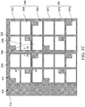
- FIG. 1C is a schematic top view of a color filter 260 and a light shielding layer 270 of some embodiments of the present invention.
- the active element array substrate 200 may comprise the color filter 260 and the light shielding layer 270.
- the color filter 260 is provided corresponding to the pixel electrodes 224, 234, and 244.
- the light shielding layer 270 defines the foregoing active region AA and peripheral region NA.
- the light shielding layer 270 may be a single-layer or a multi-layer structure, and a material thereof may be a black matrix, a material stacked by at least two color photoresists with different colors, or another suitable material, and can be formed by means of ink printing or exposure and development.
- the color filter 260 comprises a red photoresist 262, a green photoresist 264, and a blue photoresist 266.
- the red photoresist 262 is provided corresponding to the first sub-pixel region SP1.
- the green photoresist 264 is provided corresponding to the second sub-pixel region SP2.
- the blue photoresist 266 is provided corresponding to the third sub-pixel region SP3. In this way, a color of light that passes through the pixel region PR can be controlled.
- the scope of the present invention should not be limited to the color sequence.
- the blue photoresist corresponds to the first sub-pixel region SP1
- the green photoresist corresponds to the second sub-pixel region SP2
- the red photoresist corresponds to the third sub-pixel region SP3.
- the light shielding layer 270 may cover the active elements 222, 232, and 242, the first data line DL1, the second data line DL2, the third data line DL3, and capacitors (not marked) connected to the active elements.
- the light shielding layer 270 may selectively cover the common electrode line CL.
- the color filter 260 and the light shielding layer 270 may still be provided on the opposite substrate 300 (referring to FIG. ID first). In other words, the color filter 260 and the light shielding layer 270 may not be provided on the active element array substrate 200.
- FIG. ID is a schematic sectional view along a line ID-ID of FIG. 1A and FIG. 1C .
- the active element array substrate 200 is applied to a display panel 100.
- the display panel 100 comprises an active element array substrate 200, an opposite substrate 300, a liquid crystal layer 400, and an alignment layer (for example, a vertical alignment layer, not drawn).
- the liquid crystal layer 400 is provided between the active element array substrate 200 and the opposite substrate 300.
- the alignment layer (for example, a vertical alignment layer, not drawn) is respectively provided between the liquid crystal layer 400 and the active element array substrate 200 and between the liquid crystal layer 400 and the opposite substrate 300.
- the active element array substrate 200 further comprises at least one spacer 280, which is provided on the color filter 260, wherein a top end 282 of the spacer 280 is connected to the opposite substrate 300 to support/maintain a height of the liquid crystal layer 400.
- the active element 232 comprises a semiconductor layer AS, a gate (that is, the second scan line SL2 marked in the drawing), a gate dielectric layer GI, and a drain DE and a source SE that are connected to two ends of the semiconductor layer AS.
- the gate dielectric layer GI is provided between the gate and the semiconductor layer AS of the active element 232.
- the gate of the active element 232 is electrically connected to scan lines.
- the source SE of the active element 232 is electrically connected to the second data line DL2.
- the drain DE of the active element 232 is electrically connected to the connection electrode 236 and the pixel electrode 234 by means of an opening O1 of an insulation layer PL (referring to FIG. 1A and FIG. IB).
- the light shielding layer 270 may be filled into the opening O1 of the insulation layer PL to shield non-ideal light.
- the drain DE of the active element 232 is at least partially overlapping with the common electrode line CL, so as to generate capacitance to maintain a potential of the drain DE.
- a part in which the drain DE is overlapping with the common electrode line CL may be overlapping with the spacer 280, so as to reduce a range in which light cannot pass through, thereby improving an aperture opening ratio.
- overlapping in this embodiment of the present invention refers to overlapping in a vertical projection direction.
- configurations of the active elements 222 and 242 are substantively approximately the same as that of the active element 232, and details are not described herein again.
- the active elements 222, 232, and 242 may be various semiconductor elements, for example, transistors, diodes, or other suitable elements, and materials of the semiconductor elements include polysilicon, monocrystalline silicon, microcrystalline silicon, amorphous silicon, carbon nanotubes/nanorods, organic semiconductor materials, metal oxide semiconductor materials, other suitable materials, or a combination of at least two of the foregoing materials.
- the active elements 222, 232, and 242 of the present invention are transistors, they may be bottom gate transistors (for example, the gate is located below the semiconductor layer AS), top gate transistors (for example, the gate is located above the semiconductor layer AS), multi-dimensional channel transistors (for example, a carrier flowing path of the semiconductor layer AS includes two directions (for example, a horizontal direction and a non-horizontal direction)), stereoscopic transistors (for example, at least two of the gate, the source SE, and the drain DE are respectively located on different horizontal planes), or other suitable transistors.
- bottom gate transistors for example, the gate is located below the semiconductor layer AS
- top gate transistors for example, the gate is located above the semiconductor layer AS
- multi-dimensional channel transistors for example, a carrier flowing path of the semiconductor layer AS includes two directions (for example, a horizontal direction and a non-horizontal direction)
- stereoscopic transistors for example, at least two of the gate, the source SE, and the drain DE are respectively located on different horizontal planes
- the display panel 100 may use a multi-domain vertical alignment (MVA) technology.
- an alignment layer for example, a vertical alignment film, not marked
- the alignment layer may provide alignment force (for example, vertical alignment force) for liquid crystal molecules, and an electrode may further be matched to provide a plurality of pretilt angles with different domains, so that the liquid crystal layer 400 may comprise a plurality of domains to achieve the MVA technology.
- the vertical alignment layer may be formed by a polymer stabilized material. Ideally, upper and lower vertical alignment layers in any region of the liquid crystal layer 400 have a same alignment direction.
- liquid crystal display panels 100 of other types may also be used.
- the display panel 100 is a curved display panel, for example, the opposite substrate 300 and the active element array substrate 200 both bend towards a particular direction.
- a material of one of the substrate 210 of the active element array substrate 200 and the opposite substrate 300 may include glass, quartz, a polymer material (for example, polyimide (PI), benzocyclobutene (BCB), polycarbonate (PC), or another suitable material), another suitable material, or a combination of the foregoing at least two materials.
- a polymer material for example, polyimide (PI), benzocyclobutene (BCB), polycarbonate (PC), or another suitable material
- PC polycarbonate
- the insulation layer PL and the gate dielectric layer GI may be single-layer or multi-layer structures, and materials thereof include (for example, silicon oxide, silicon nitride, silicon oxynitride, or other suitable materials), organic materials (for example, photoresists, PI, BCB, or other suitable materials), or other suitable materials.
- the data lines DL1 to DL3, the scan lines SL1 to SL2 and the common electrode line CL may be various materials with good conductivity, for example, metals, alloys, conductive adhesives, other suitable materials, or a combination of the foregoing at least two materials.
- the pixel electrodes 224 to 244 and the connection electrodes 226 to 246 may be formed by patterning a same material layer, wherein the material layer may be formed by various materials with good conductivity and transparency, for example, indium tin oxide. In other embodiments, the pixel electrodes 224 to 244 and the connection electrodes 226 to 246 may be formed by patterning different material layers.
- FIG. 1E is a schematic sectional view along a line IE-IE of FIG. 1A and FIG. 1C .
- the light shielding layer 270 is provided between adjacent two pixel regions PR to cover the first data line DL1, the third data line DL3, and a gap therebetween, so as to preferably distinguish the two pixel regions PR from each other.
- a projection of the shield electrode 290 on the substrate 210 is at least partially located outside a projection of the light shielding layer 270 on the substrate 210, so as to increase a shielded region, and ensure that electric fields of the first data line DL1 and the third data line DL3 do not escape to affect liquid crystal arrangement.
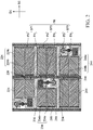
- FIG. 2 is a schematic top view of a single pixel region PR according to another embodiment of the present invention.
- the present embodiment is similar to the embodiment of FIG. 1B , and the difference lies in that: in the present embodiment, pixel electrodes 224, 234, and 244 do not comprise first trunk electrodes 224a, 234a, and 244a (referring to FIG. IB), and branch electrodes 224c, 234c, and 244c of the pixel electrodes 224, 234, and 244 have two extension directions.
- quantities of the pixel electrodes 224, 234, and 244 may be plural, and the pixel electrodes 224, 234, and 244 are distributed in different regions of the first sub-pixel region SP1, the second sub-pixel region SP2, and the third sub-pixel region SP3.
- the pixel electrodes 224, 234, and 244 may be designed not to comprise the first trunk electrodes 224a, 234a, and 244a (referring to FIG. IB).
- a shield electrode 290 is designed to shield a dislocated region on one side of a first divided region PA and a second divided region PB, and therefore an area of the dislocated region may be reduced, to reduce an effect of the black feature phenomenon on visual effects.
- the embodiments of the present invention provide an active element array substrate and a curved display panel using the same.
- a long edge of a sub-pixel is designed to be parallel to a long edge of a display panel, so that a region in which liquid crystal arrangement is disordered because upper and lower substrates are dislocated is reduced.
- a first sub-pixel unit 220, a second sub-pixel unit 230, and a third sub-pixel unit 240 are supplied with respective operating voltages by means of a same gate signal and different data signals to present expected brightnesses. This practice may improve power supply time of each sub-pixel unit to ensure that an active element in each sub-pixel unit is sufficiently charged.
Landscapes
- Physics & Mathematics (AREA)
- Nonlinear Science (AREA)
- Engineering & Computer Science (AREA)
- General Physics & Mathematics (AREA)
- Chemical & Material Sciences (AREA)
- Crystallography & Structural Chemistry (AREA)
- Optics & Photonics (AREA)
- Mathematical Physics (AREA)
- Microelectronics & Electronic Packaging (AREA)
- Theoretical Computer Science (AREA)
- Geometry (AREA)
- General Engineering & Computer Science (AREA)
- Computer Hardware Design (AREA)
- Liquid Crystal (AREA)
- Human Computer Interaction (AREA)
- Spectroscopy & Molecular Physics (AREA)
- Devices For Indicating Variable Information By Combining Individual Elements (AREA)
- Health & Medical Sciences (AREA)
- Life Sciences & Earth Sciences (AREA)
- Chemical Kinetics & Catalysis (AREA)
- Electrochemistry (AREA)
- Molecular Biology (AREA)
- Electromagnetism (AREA)
Claims (15)
- Aktives-Element-Array-Substrat (200) eines gekrümmten Flüssigkristallanzeigefelds (100), umfassend:ein Substrat (210), das eine aktive Region (AA) und eine periphere Region (NA) umfasst;eine erste Datenleitung (DL1), die auf dem Substrat (210) angeordnet ist und sich entlang einer ersten Richtung (D1) erstreckt;eine zweite Datenleitung (DL2), die auf dem Substrat (210) angeordnet ist und sich entlang der ersten Richtung (D1) erstreckt;eine dritte Datenleitung (DL3), die auf dem Substrat (210) angeordnet ist und sich entlang der ersten Richtung (D1) erstreckt, wobei die zweite Datenleitung (DL2) zwischen der ersten Datenleitung (DL1) und der dritten Datenleitung (DL3) liegt;wenigstens eine erste Abtastleitung (SL1), die auf dem Substrat (210) angeordnet ist und sich entlang einer zweiten Richtung (D2) erstreckt, wobei die zweite Richtung (D2) von der ersten Richtung (D1) verschieden ist und diese schneidet;eine zweite Abtastleitung (SL2), die auf dem Substrat (210) angeordnet ist und sich entlang der zweiten Richtung (D2) erstreckt;eine gemeinsame Elektrodenleitung (CL), die auf dem Substrat (210) angeordnet ist und sich entlang der zweiten Richtung (D2) erstreckt, wobei die gemeinsame Elektrodenleitung (CL) zwischen der ersten Abtastleitung (SL1) und der zweiten Abtastleitung (SL2) liegt;wenigstens eine Pixelregion (PR);eine erste Teilpixeleinheit (220) in der Pixelregion (PR), die elektrisch mit der ersten Datenleitung (DL1) und der ersten Abtastleitung (SL1) verbunden ist;eine zweite Teilpixeleinheit (230) in der Pixelregion (PR), die elektrisch mit der zweiten Datenleitung (DL2) und der zweiten Abtastleitung (SL2) verbunden ist; undeine dritte Teilpixeleinheit (240) in der Pixelregion (PR), die elektrisch mit der dritten Datenleitung (DL3) und der zweiten Abtastleitung (SL2) verbunden ist, wobei die erste Teilpixeleinheit (220), die zweite Teilpixeleinheit (230) und die dritte Teilpixeleinheit (240) in einer Biegerichtung des gekrümmten Flüssigkristallanzeigefelds (100) langgestreckt sind und sich zwischen der ersten Datenleitung (DL1) und der dritten Datenleitung (DL3) erstrecken, und wobei die gemeinsame Elektrodenleitung (CL) zwischen der ersten Teilpixeleinheit (220) und der zweiten Teilpixeleinheit (230) angeordnet ist, wobei die zweite Abtastleitung (SL2) zwischen der zweiten Teilpixeleinheit (230) und der dritten Teilpixeleinheit (240) angeordnet ist und die wenigstens eine Abtastleitung (Sll) auf der gegenüberliegenden Seite der ersten Teilpixeleinheit (220) in Bezug auf die gemeinsame Elektrodenleitung (CL) angeordnet ist.
- Aktives-Element-Array-Substrat (200) nach Anspruch 1, dadurch gekennzeichnet, dass die erste Datenleitung (DL1) von der dritten Datenleitung (DL3) um eine erste Länge in der Biegerichtung des gekrümmten Flüssigkristallfelds (100) beabstandet ist, die erste Abtastleitung (SL1) von der gemeinsamen Elektrodenleitung (CL) um eine zweite Länge beabstandet ist und die erste Länge größer als die zweite Länge ist.
- Aktives-Element-Array-Substrat (200) nach Anspruch 1, dadurch gekennzeichnet, dass sich die erste Abtastleitung (SL1) und die zweite Abtastleitung (SL2) bis zu der peripheren Region (NA) erstrecken und die erste Abtastleitung (SL1) mit der zweiten Abtastleitung (SL2) elektrisch verbunden ist.
- Aktives-Element-Array-Substrat (200) nach Anspruch 3, dadurch gekennzeichnet, dass es ferner einen Gate-Treiber (250) umfasst, der in der peripheren Region (NA) angeordnet ist, wobei der Gate-Treiber (250) einen ersten Pin umfasst und sowohl die erste Abtastleitung (SL1) als auch die zweite Abtastleitung (SL2) elektrisch mit dem ersten Pin verbunden sind.
- Aktives-Element-Array-Substrat (200) nach Anspruch 1, dadurch gekennzeichnet, dass die erste Teilpixeleinheit (220), die zweite Teilpixeleinheit (230) oder die dritte Teilpixeleinheit (240) ein aktives Element (222, 232 oder 242) und eine erste Pixelelektrode (224, 234 oder 244) umfasst, und die erste Pixelelektrode (224, 234 oder 244) elektrisch mit dem aktiven Element (222, 232 oder 242) verbunden ist, und die erste Pixelelektrode (224, 234 oder 244) umfasst:eine erste Stammelektrode (224b, 234b oder 244b), die sich entlang der zweiten Richtung (D2) erstreckt; undeine Mehrzahl von ersten Zweigelektroden (224c, 234c oder 244c), die elektrisch mit der ersten Stammelektrode (224b, 234b oder 244b) verbunden sind und sich in eine Mehrzahl von verschiedenen Erstreckungsrichtungen erstrecken, wobei die Erstreckungsrichtungen von der ersten Richtung (D1) und der zweiten Richtung (D2) verschieden sind.
- Aktives-Element-Array-Substrat (200) nach Anspruch 5, wobei die erste Teilpixeleinheit (220), die zweite Teilpixeleinheit (230) oder die dritte Teilpixeleinheit (240) ferner umfasst:
eine zweite Stammelektrode (224a, 234a oder 244a), die sich entlang der ersten Richtung (D1) erstreckt und die erste Stammelektrode (224b, 234b oder 244b) schneidet. - Aktives-Element-Array-Substrat (200) nach Anspruch 5, dadurch gekennzeichnet, dass jede der ersten Teilpixeleinheit (220), der zweiten Teilpixeleinheit (230) oder der dritten Teilpixeleinheit (240) ferner eine zweite Pixelelektrode (224, 234 oder 244) und eine Verbindungselektrode (226, 236 oder 246) umfasst, wobei die erste Pixelelektrode (224, 234 oder 244) und die zweite Pixelelektrode (224, 234 oder 244) über die Verbindungselektrode (226, 236 oder 246) verbunden sind und die zweite Pixelelektrode (224, 234 oder 244) eine zweite Stammelektrode (224b, 234b oder 244b) und eine Mehrzahl von zweiten Stammelektroden (224c, 234c oder 244c) umfasst; und die zweite Datenleitung (DL2) zwischen der ersten Pixelelektrode (224, 234 oder 244) und der zweiten Pixelelektrode (224, 234 oder 244) positioniert ist.
- Aktives-Element-Array-Substrat (200) nach Anspruch 7, dadurch gekennzeichnet, dass die Mehrzahl von ersten Zweigelektroden (224c, 234c oder 244c) eine erste Erstreckungsrichtung und eine zweite Erstreckungsrichtung aufweisen.
- Aktives-Element-Array-Substrat (200) nach Anspruch 7, dadurch gekennzeichnet, dass die Mehrzahl von ersten Zweigelektroden (224c, 234c oder 244c) und die Mehrzahl von zweiten Zweigelektroden (224c, 234c oder 244c) eine erste Erstreckungsrichtung, eine zweite Erstreckungsrichtung, eine dritte Erstreckungsrichtung und eine vierte Erstreckungsrichtung aufweisen.
- Aktives-Element-Array-Substrat (200) nach Anspruch 1, dadurch gekennzeichnet, dass die erste Datenleitung (DL1) und die dritte Datenleitung (DL3) eine Mehrzahl der ersten Abtastleitungen (SL1) schneiden, um die wenigstens eine Pixelregion (PR) auszubilden, und die Pixelregion (PR) eine erste Teilpixelregion (SP1), eine zweite Teilpixelregion (SP2) und eine dritte Teilpixelregion (SP3) aufweist, wobei die erste Teilpixeleinheit (220), die zweite Teilpixeleinheit (230) und die dritte Teilpixeleinheit (240) entsprechend in der ersten Teilpixelregion (SP1), der zweiten Teilpixelregion (SP2) und der dritten Teilpixelregion (SP3) angeordnet sind, wobei jede der ersten Teilpixeleinheit (220), der zweiten Teilpixeleinheit (230) und der dritten Teilpixeleinheit (240) ein aktives Element (222, 232 oder 242) und eine Pixelelektrode (224, 234 oder 244) umfasst, und die Pixelelektrode (224, 234 oder 244) elektrisch mit dem aktiven Element (222, 232 oder 242) verbunden ist, und das aktive Element-Array-Substrat (200) ferner umfasst:einen Farbfilter (260), umfassend:einen roten Fotolack (262), der entsprechend der Pixelelektrode (224, 234 oder 244) der ersten Teilpixelregion (SP1) bereitgestellt ist;einen grünen Fotolack (264), der entsprechend der Pixelelektrode (224, 234 oder 244) der zweiten Teilpixelregion (SP2) bereitgestellt ist; undeinen blauen Fotolack (266), der entsprechend der Pixelelektrode (224, 234 oder 244) der dritten Teilpixelregion (SP3) bereitgestellt ist; undeine lichtabschirmende Schicht (270) über dem aktiven Element (222, 232 oder 242).
- Gekrümmtes Anzeigefeld (100), dadurch gekennzeichnet, dass sie umfasst:das aktive Element-Array-Substrat (200) nach Anspruch 1;ein gegenüberliegendes Substrat (300);eine Flüssigkristallschicht (400), die zwischen dem aktiven Element-Array-Substrat (200) und dem gegenüberliegenden Substrat (300) vorgesehen ist; undzwei vertikale Ausrichtungsschichten, die jeweils zwischen der Flüssigkristallschicht (400) und dem aktiven Element-Array-Substrat (200) und zwischen der Flüssigkristallschicht (400) und dem gegenüberliegenden Substrat (300) vorgesehen sind.
- Gekrümmtes Anzeigefeld (100) nach Anspruch 11, dadurch gekennzeichnet, dass die vertikalen Ausrichtungsschichten durch polymerstabilisierte Materialien ausgebildet sind.
- Gekrümmtes Anzeigefeld (100) nach Anspruch 11, dadurch gekennzeichnet, dass jede der ersten Teilpixeleinheit (220), der zweiten Teilpixeleinheit (230) und der dritten Teilpixeleinheit (240) ein aktives Element (222, 232 oder 242) und eine Pixelelektrode (224, 234 oder 244) umfasst, und die Pixelelektrode (224, 234 oder 244) elektrisch mit dem aktiven Element (222, 232 oder 242) verbunden ist, und das aktive Element-Array-Substrat (200) ferner umfasst:einen Farbfilter (260), der entsprechend der Pixelelektrode (224, 234 oder 244) bereitgestellt ist;eine lichtabschirmende Schicht (270), die entsprechend dem aktiven Element (222, 232 oder 242) bereitgestellt ist; undwenigstens einen Abstandshalter (280), der an dem Farbfilter (260) vorgesehen ist, wobei ein oberes Ende des Abstandshalters (280) mit dem gegenüberliegenden Substrat (300) verbunden ist.
- Gekrümmtes Anzeigefeld (100) nach Anspruch 11, wobei sich das Substrat (210) des aktiven Element-Array-Substrats (200) und das gegenüberliegende Substrat (300) entlang der zweiten Richtung (D2) biegen.
- Gekrümmtes Anzeigefeld (100) nach Anspruch 11, dadurch gekennzeichnet, dass die erste Datenleitung (DL1) und die dritte Datenleitung (DL3) eine Mehrzahl der ersten Abtastleitungen (SL1) schneiden, um die wenigstens eine Pixelregion (PR) auszubilden, und die Pixelregion (PR) eine erste Teilpixelregion (SP1), eine zweite Teilpixelregion (SP2) und eine dritte Teilpixelregion (SP3) aufweist, die durch die zweite Abtastleitung (SL2) und die gemeinsame Elektrodenleitung (CL) getrennt sind, wobei die erste Teilpixeleinheit (220), die zweite Teilpixeleinheit (230) und die dritte Teilpixeleinheit (240) entsprechend in der ersten Teilpixelregion (SP1), der zweiten Teilpixelregion (SP2) und der dritten Teilpixelregion (SP3) angeordnet sind, wobei jeder der ersten Teilpixelregion (SP1), der zweiten Teilpixelregion (SP2) und der dritten Teilpixelregion (SP3) eine erste Länge (L1) in der ersten Richtung (D1) aufweist und eine zweite Länge (L2) in der zweiten, der sich biegenden Richtung (D2) des gekrümmten Anzeigefelds (100) aufweist, und die erste Länge (L1) kleiner als die zweite Länge (L2) ist.
Applications Claiming Priority (1)
| Application Number | Priority Date | Filing Date | Title |
|---|---|---|---|
| TW105143686A TWI589972B (zh) | 2016-12-28 | 2016-12-28 | 主動元件陣列基板及應用其之液晶面板 |
Publications (2)
| Publication Number | Publication Date |
|---|---|
| EP3343283A1 EP3343283A1 (de) | 2018-07-04 |
| EP3343283B1 true EP3343283B1 (de) | 2021-09-01 |
Family
ID=59133535
Family Applications (1)
| Application Number | Title | Priority Date | Filing Date |
|---|---|---|---|
| EP17200119.0A Active EP3343283B1 (de) | 2016-12-28 | 2017-11-06 | Aktives element-array-substrat und anzeigetafel damit |
Country Status (4)
| Country | Link |
|---|---|
| US (1) | US9933678B1 (de) |
| EP (1) | EP3343283B1 (de) |
| CN (1) | CN106842746B (de) |
| TW (1) | TWI589972B (de) |
Families Citing this family (16)
| Publication number | Priority date | Publication date | Assignee | Title |
|---|---|---|---|---|
| CN108628045B (zh) * | 2017-03-21 | 2022-01-25 | 京东方科技集团股份有限公司 | 阵列基板、显示面板和显示装置 |
| CN107329311B (zh) * | 2017-08-03 | 2020-04-28 | 深圳市华星光电技术有限公司 | 阵列基板及液晶显示面板 |
| KR102351618B1 (ko) | 2017-08-28 | 2022-01-17 | 삼성디스플레이 주식회사 | 표시장치 |
| TWI649607B (zh) * | 2017-11-20 | 2019-02-01 | 友達光電股份有限公司 | 畫素結構及曲面顯示裝置 |
| CN110246988A (zh) * | 2018-03-09 | 2019-09-17 | 上海和辉光电有限公司 | 一种显示面板及其制造方法、显示母板以及显示装置 |
| CN110456576B (zh) * | 2018-05-08 | 2022-05-13 | 群创光电股份有限公司 | 显示设备 |
| CN110556078A (zh) * | 2018-06-01 | 2019-12-10 | 中华映管股份有限公司 | 显示装置 |
| CN109375433A (zh) * | 2018-10-30 | 2019-02-22 | 惠科股份有限公司 | 一种显示面板的像素电极及显示面板、显示装置 |
| TWI711852B (zh) * | 2019-05-15 | 2020-12-01 | 友達光電股份有限公司 | 顯示面板及其製造方法 |
| US12235553B2 (en) | 2020-12-04 | 2025-02-25 | Beijing Boe Display Technology Co., Ltd. | Array substrate and display panel |
| US12150353B2 (en) | 2021-02-08 | 2024-11-19 | Boe Technology Group Co., Ltd. | Display substrate and display apparatus |
| CN113820883A (zh) * | 2021-09-29 | 2021-12-21 | Tcl华星光电技术有限公司 | 显示面板的像素单元及显示面板 |
| US11953795B2 (en) | 2021-09-29 | 2024-04-09 | Tcl China Star Optoelectronics Technology Co., Ltd. | Pixel unit of a display panel and display panel |
| KR20230055471A (ko) * | 2021-10-18 | 2023-04-26 | 삼성디스플레이 주식회사 | 디스플레이 장치 |
| TWI779899B (zh) * | 2021-10-25 | 2022-10-01 | 友達光電股份有限公司 | 顯示裝置 |
| CN119446010A (zh) * | 2023-07-28 | 2025-02-14 | 北京京东方显示技术有限公司 | 阵列基板、驱动方法和显示装置 |
Family Cites Families (25)
| Publication number | Priority date | Publication date | Assignee | Title |
|---|---|---|---|---|
| KR100998640B1 (ko) * | 2003-12-23 | 2010-12-06 | 엘지디스플레이 주식회사 | 액정표시장치 및 그 제조방법 |
| KR101187207B1 (ko) * | 2005-08-04 | 2012-10-02 | 삼성디스플레이 주식회사 | 디스플레이장치 |
| CN100495179C (zh) * | 2006-08-09 | 2009-06-03 | 友达光电股份有限公司 | 液晶显示器 |
| JP5191639B2 (ja) | 2006-09-15 | 2013-05-08 | 株式会社ジャパンディスプレイイースト | 液晶表示装置 |
| JP5322427B2 (ja) * | 2007-12-19 | 2013-10-23 | 三菱電機株式会社 | 液晶表示装置 |
| TWI408477B (zh) * | 2009-12-30 | 2013-09-11 | Au Optronics Corp | 畫素陣列以及聚合物穩定配向液晶顯示面板 |
| TWI420212B (zh) * | 2009-12-31 | 2013-12-21 | Au Optronics Corp | 畫素陣列 |
| KR101817791B1 (ko) * | 2010-12-14 | 2018-01-12 | 삼성디스플레이 주식회사 | 액정 표시 장치 |
| KR20120111684A (ko) | 2011-04-01 | 2012-10-10 | 엘지디스플레이 주식회사 | 액정표시장치 |
| CN102930809B (zh) | 2011-08-12 | 2016-02-10 | 上海中航光电子有限公司 | 双栅极驱动的横向排列的像素结构及显示面板 |
| CN103135295B (zh) | 2011-11-29 | 2015-09-30 | 上海中航光电子有限公司 | 双栅极驱动的横向像素结构及液晶显示器 |
| CN103176320B (zh) * | 2011-12-22 | 2015-12-09 | 上海中航光电子有限公司 | 横向排列的像素结构、液晶显示装置及其制作方法 |
| KR101622655B1 (ko) * | 2012-03-14 | 2016-05-19 | 엘지디스플레이 주식회사 | 액정 표시 장치 및 이의 제조 방법 |
| TWI481937B (zh) * | 2012-08-27 | 2015-04-21 | Au Optronics Corp | 顯示面板 |
| CN103278977B (zh) * | 2013-05-31 | 2015-11-25 | 深圳市华星光电技术有限公司 | 液晶显示面板及其像素结构和驱动方法 |
| TWI572963B (zh) * | 2014-02-12 | 2017-03-01 | 友達光電股份有限公司 | 顯示面板 |
| JP2015184418A (ja) * | 2014-03-24 | 2015-10-22 | 株式会社ジャパンディスプレイ | 液晶表示装置 |
| CN104375339B (zh) * | 2014-11-13 | 2017-07-18 | 深圳市华星光电技术有限公司 | 曲面液晶显示面板及曲面液晶显示装置 |
| KR102307814B1 (ko) * | 2015-04-16 | 2021-10-01 | 삼성디스플레이 주식회사 | 액정 표시 장치 |
| TWI638209B (zh) * | 2015-05-05 | 2018-10-11 | 友達光電股份有限公司 | 顯示面板 |
| TWI561890B (en) * | 2015-08-10 | 2016-12-11 | Au Optronics Corp | Pixel array, display panel and curved display panel |
| CN105259716B (zh) * | 2015-11-24 | 2018-08-03 | 京东方科技集团股份有限公司 | 一种阵列基板、曲面显示面板及曲面显示装置 |
| TWI560494B (en) * | 2015-12-24 | 2016-12-01 | Au Optronics Corp | Display device |
| TW201734605A (zh) * | 2016-03-18 | 2017-10-01 | 友達光電股份有限公司 | 陣列基板以及曲面液晶顯示面板 |
| TWI613487B (zh) * | 2016-03-28 | 2018-02-01 | 友達光電股份有限公司 | 曲面顯示面板 |
-
2016
- 2016-12-28 TW TW105143686A patent/TWI589972B/zh active
-
2017
- 2017-02-21 CN CN201710092059.1A patent/CN106842746B/zh active Active
- 2017-07-17 US US15/651,054 patent/US9933678B1/en active Active
- 2017-11-06 EP EP17200119.0A patent/EP3343283B1/de active Active
Also Published As
| Publication number | Publication date |
|---|---|
| EP3343283A1 (de) | 2018-07-04 |
| TW201823829A (zh) | 2018-07-01 |
| US9933678B1 (en) | 2018-04-03 |
| CN106842746B (zh) | 2020-07-14 |
| CN106842746A (zh) | 2017-06-13 |
| TWI589972B (zh) | 2017-07-01 |
Similar Documents
| Publication | Publication Date | Title |
|---|---|---|
| US9933678B1 (en) | Active element array substrate and display panel using the same | |
| US7728941B2 (en) | Liquid crystal display device and method for manufacturing the same | |
| US8976328B2 (en) | Liquid crystal display device and method for fabricating the same | |
| EP2980636B1 (de) | Flüssigkristallanzeigetafel | |
| CN103869554B (zh) | 液晶显示面板 | |
| US7206050B2 (en) | IPS type LCD and method for fabricating the same | |
| CN102809855B (zh) | 薄膜晶体管基板及其制造方法 | |
| US9678395B1 (en) | Array substrate and curved liquid crystal display panel | |
| US9853060B2 (en) | Thin film transistor substrate and method of manufacturing the same | |
| CN110967882B (zh) | 显示设备 | |
| US7995164B2 (en) | Array substrate having a particular light shielding portion in the non-display region | |
| KR20180049371A (ko) | 초고 해상도 액정 표시장치 | |
| US20160026049A1 (en) | Thin-film transistor substrate and display panel having the same | |
| US7936407B2 (en) | Array substrate, method of manufacturing the same, display panel having the same, and liquid crystal display apparatus having the same | |
| US20080084528A1 (en) | Liquid crystal display device | |
| US20160291409A1 (en) | Liquid crystal display including pixel and auxiliary electrodes within display substrate | |
| US20060028604A1 (en) | Liquid crystal display device | |
| US10890815B2 (en) | Display apparatus | |
| US12235553B2 (en) | Array substrate and display panel | |
| KR101282402B1 (ko) | 액정표시장치 | |
| KR101260989B1 (ko) | 액정표시패널 및 그 제조방법 | |
| US11003031B2 (en) | Display apparatus | |
| KR20080053804A (ko) | 액정표시장치와 그 제조방법 | |
| KR20160002551A (ko) | 보상용 박막 트랜지스터를 구비한 초고 해상도 액정 표시장치 | |
| KR20170033935A (ko) | 보상용 박막 트랜지스터를 구비한 액정 표시장치 |
Legal Events
| Date | Code | Title | Description |
|---|---|---|---|
| PUAI | Public reference made under article 153(3) epc to a published international application that has entered the european phase |
Free format text: ORIGINAL CODE: 0009012 |
|
| STAA | Information on the status of an ep patent application or granted ep patent |
Free format text: STATUS: REQUEST FOR EXAMINATION WAS MADE |
|
| 17P | Request for examination filed |
Effective date: 20171106 |
|
| AK | Designated contracting states |
Kind code of ref document: A1 Designated state(s): AL AT BE BG CH CY CZ DE DK EE ES FI FR GB GR HR HU IE IS IT LI LT LU LV MC MK MT NL NO PL PT RO RS SE SI SK SM TR |
|
| AX | Request for extension of the european patent |
Extension state: BA ME |
|
| GRAP | Despatch of communication of intention to grant a patent |
Free format text: ORIGINAL CODE: EPIDOSNIGR1 |
|
| STAA | Information on the status of an ep patent application or granted ep patent |
Free format text: STATUS: GRANT OF PATENT IS INTENDED |
|
| RIC1 | Information provided on ipc code assigned before grant |
Ipc: G02F 1/1337 20060101ALN20210323BHEP Ipc: G09G 3/36 20060101ALI20210323BHEP Ipc: H01L 27/32 20060101ALI20210323BHEP Ipc: G09G 3/34 20060101ALI20210323BHEP Ipc: H01L 27/12 20060101ALI20210323BHEP Ipc: G02F 1/1362 20060101ALI20210323BHEP Ipc: G02F 1/1343 20060101AFI20210323BHEP |
|
| INTG | Intention to grant announced |
Effective date: 20210421 |
|
| RIC1 | Information provided on ipc code assigned before grant |
Ipc: G02F 1/1337 20060101ALN20210412BHEP Ipc: G09G 3/36 20060101ALI20210412BHEP Ipc: H01L 27/32 20060101ALI20210412BHEP Ipc: G09G 3/34 20060101ALI20210412BHEP Ipc: H01L 27/12 20060101ALI20210412BHEP Ipc: G02F 1/1362 20060101ALI20210412BHEP Ipc: G02F 1/1343 20060101AFI20210412BHEP |
|
| GRAS | Grant fee paid |
Free format text: ORIGINAL CODE: EPIDOSNIGR3 |
|
| GRAA | (expected) grant |
Free format text: ORIGINAL CODE: 0009210 |
|
| STAA | Information on the status of an ep patent application or granted ep patent |
Free format text: STATUS: THE PATENT HAS BEEN GRANTED |
|
| AK | Designated contracting states |
Kind code of ref document: B1 Designated state(s): AL AT BE BG CH CY CZ DE DK EE ES FI FR GB GR HR HU IE IS IT LI LT LU LV MC MK MT NL NO PL PT RO RS SE SI SK SM TR |
|
| REG | Reference to a national code |
Ref country code: GB Ref legal event code: FG4D |
|
| REG | Reference to a national code |
Ref country code: CH Ref legal event code: EP Ref country code: AT Ref legal event code: REF Ref document number: 1426845 Country of ref document: AT Kind code of ref document: T Effective date: 20210915 |
|
| REG | Reference to a national code |
Ref country code: DE Ref legal event code: R096 Ref document number: 602017045075 Country of ref document: DE |
|
| REG | Reference to a national code |
Ref country code: IE Ref legal event code: FG4D |
|
| REG | Reference to a national code |
Ref country code: LT Ref legal event code: MG9D |
|
| REG | Reference to a national code |
Ref country code: NL Ref legal event code: MP Effective date: 20210901 |
|
| PG25 | Lapsed in a contracting state [announced via postgrant information from national office to epo] |
Ref country code: RS Free format text: LAPSE BECAUSE OF FAILURE TO SUBMIT A TRANSLATION OF THE DESCRIPTION OR TO PAY THE FEE WITHIN THE PRESCRIBED TIME-LIMIT Effective date: 20210901 Ref country code: SE Free format text: LAPSE BECAUSE OF FAILURE TO SUBMIT A TRANSLATION OF THE DESCRIPTION OR TO PAY THE FEE WITHIN THE PRESCRIBED TIME-LIMIT Effective date: 20210901 Ref country code: HR Free format text: LAPSE BECAUSE OF FAILURE TO SUBMIT A TRANSLATION OF THE DESCRIPTION OR TO PAY THE FEE WITHIN THE PRESCRIBED TIME-LIMIT Effective date: 20210901 Ref country code: FI Free format text: LAPSE BECAUSE OF FAILURE TO SUBMIT A TRANSLATION OF THE DESCRIPTION OR TO PAY THE FEE WITHIN THE PRESCRIBED TIME-LIMIT Effective date: 20210901 Ref country code: ES Free format text: LAPSE BECAUSE OF FAILURE TO SUBMIT A TRANSLATION OF THE DESCRIPTION OR TO PAY THE FEE WITHIN THE PRESCRIBED TIME-LIMIT Effective date: 20210901 Ref country code: NO Free format text: LAPSE BECAUSE OF FAILURE TO SUBMIT A TRANSLATION OF THE DESCRIPTION OR TO PAY THE FEE WITHIN THE PRESCRIBED TIME-LIMIT Effective date: 20211201 Ref country code: BG Free format text: LAPSE BECAUSE OF FAILURE TO SUBMIT A TRANSLATION OF THE DESCRIPTION OR TO PAY THE FEE WITHIN THE PRESCRIBED TIME-LIMIT Effective date: 20211201 Ref country code: LT Free format text: LAPSE BECAUSE OF FAILURE TO SUBMIT A TRANSLATION OF THE DESCRIPTION OR TO PAY THE FEE WITHIN THE PRESCRIBED TIME-LIMIT Effective date: 20210901 |
|
| REG | Reference to a national code |
Ref country code: AT Ref legal event code: MK05 Ref document number: 1426845 Country of ref document: AT Kind code of ref document: T Effective date: 20210901 |
|
| PG25 | Lapsed in a contracting state [announced via postgrant information from national office to epo] |
Ref country code: PL Free format text: LAPSE BECAUSE OF FAILURE TO SUBMIT A TRANSLATION OF THE DESCRIPTION OR TO PAY THE FEE WITHIN THE PRESCRIBED TIME-LIMIT Effective date: 20210901 Ref country code: LV Free format text: LAPSE BECAUSE OF FAILURE TO SUBMIT A TRANSLATION OF THE DESCRIPTION OR TO PAY THE FEE WITHIN THE PRESCRIBED TIME-LIMIT Effective date: 20210901 Ref country code: GR Free format text: LAPSE BECAUSE OF FAILURE TO SUBMIT A TRANSLATION OF THE DESCRIPTION OR TO PAY THE FEE WITHIN THE PRESCRIBED TIME-LIMIT Effective date: 20211202 |
|
| PG25 | Lapsed in a contracting state [announced via postgrant information from national office to epo] |
Ref country code: AT Free format text: LAPSE BECAUSE OF FAILURE TO SUBMIT A TRANSLATION OF THE DESCRIPTION OR TO PAY THE FEE WITHIN THE PRESCRIBED TIME-LIMIT Effective date: 20210901 |
|
| PG25 | Lapsed in a contracting state [announced via postgrant information from national office to epo] |
Ref country code: IS Free format text: LAPSE BECAUSE OF FAILURE TO SUBMIT A TRANSLATION OF THE DESCRIPTION OR TO PAY THE FEE WITHIN THE PRESCRIBED TIME-LIMIT Effective date: 20220101 Ref country code: SM Free format text: LAPSE BECAUSE OF FAILURE TO SUBMIT A TRANSLATION OF THE DESCRIPTION OR TO PAY THE FEE WITHIN THE PRESCRIBED TIME-LIMIT Effective date: 20210901 Ref country code: SK Free format text: LAPSE BECAUSE OF FAILURE TO SUBMIT A TRANSLATION OF THE DESCRIPTION OR TO PAY THE FEE WITHIN THE PRESCRIBED TIME-LIMIT Effective date: 20210901 Ref country code: RO Free format text: LAPSE BECAUSE OF FAILURE TO SUBMIT A TRANSLATION OF THE DESCRIPTION OR TO PAY THE FEE WITHIN THE PRESCRIBED TIME-LIMIT Effective date: 20210901 Ref country code: PT Free format text: LAPSE BECAUSE OF FAILURE TO SUBMIT A TRANSLATION OF THE DESCRIPTION OR TO PAY THE FEE WITHIN THE PRESCRIBED TIME-LIMIT Effective date: 20220103 Ref country code: NL Free format text: LAPSE BECAUSE OF FAILURE TO SUBMIT A TRANSLATION OF THE DESCRIPTION OR TO PAY THE FEE WITHIN THE PRESCRIBED TIME-LIMIT Effective date: 20210901 Ref country code: EE Free format text: LAPSE BECAUSE OF FAILURE TO SUBMIT A TRANSLATION OF THE DESCRIPTION OR TO PAY THE FEE WITHIN THE PRESCRIBED TIME-LIMIT Effective date: 20210901 Ref country code: CZ Free format text: LAPSE BECAUSE OF FAILURE TO SUBMIT A TRANSLATION OF THE DESCRIPTION OR TO PAY THE FEE WITHIN THE PRESCRIBED TIME-LIMIT Effective date: 20210901 Ref country code: AL Free format text: LAPSE BECAUSE OF FAILURE TO SUBMIT A TRANSLATION OF THE DESCRIPTION OR TO PAY THE FEE WITHIN THE PRESCRIBED TIME-LIMIT Effective date: 20210901 |
|
| REG | Reference to a national code |
Ref country code: DE Ref legal event code: R097 Ref document number: 602017045075 Country of ref document: DE |
|
| PG25 | Lapsed in a contracting state [announced via postgrant information from national office to epo] |
Ref country code: MC Free format text: LAPSE BECAUSE OF FAILURE TO SUBMIT A TRANSLATION OF THE DESCRIPTION OR TO PAY THE FEE WITHIN THE PRESCRIBED TIME-LIMIT Effective date: 20210901 |
|
| REG | Reference to a national code |
Ref country code: CH Ref legal event code: PL |
|
| PLBE | No opposition filed within time limit |
Free format text: ORIGINAL CODE: 0009261 |
|
| STAA | Information on the status of an ep patent application or granted ep patent |
Free format text: STATUS: NO OPPOSITION FILED WITHIN TIME LIMIT |
|
| PG25 | Lapsed in a contracting state [announced via postgrant information from national office to epo] |
Ref country code: LU Free format text: LAPSE BECAUSE OF NON-PAYMENT OF DUE FEES Effective date: 20211106 Ref country code: IT Free format text: LAPSE BECAUSE OF FAILURE TO SUBMIT A TRANSLATION OF THE DESCRIPTION OR TO PAY THE FEE WITHIN THE PRESCRIBED TIME-LIMIT Effective date: 20210901 Ref country code: DK Free format text: LAPSE BECAUSE OF FAILURE TO SUBMIT A TRANSLATION OF THE DESCRIPTION OR TO PAY THE FEE WITHIN THE PRESCRIBED TIME-LIMIT Effective date: 20210901 Ref country code: BE Free format text: LAPSE BECAUSE OF NON-PAYMENT OF DUE FEES Effective date: 20211130 |
|
| REG | Reference to a national code |
Ref country code: BE Ref legal event code: MM Effective date: 20211130 |
|
| 26N | No opposition filed |
Effective date: 20220602 |
|
| PG25 | Lapsed in a contracting state [announced via postgrant information from national office to epo] |
Ref country code: SI Free format text: LAPSE BECAUSE OF FAILURE TO SUBMIT A TRANSLATION OF THE DESCRIPTION OR TO PAY THE FEE WITHIN THE PRESCRIBED TIME-LIMIT Effective date: 20210901 Ref country code: LI Free format text: LAPSE BECAUSE OF NON-PAYMENT OF DUE FEES Effective date: 20211130 Ref country code: CH Free format text: LAPSE BECAUSE OF NON-PAYMENT OF DUE FEES Effective date: 20211130 |
|
| PG25 | Lapsed in a contracting state [announced via postgrant information from national office to epo] |
Ref country code: IE Free format text: LAPSE BECAUSE OF NON-PAYMENT OF DUE FEES Effective date: 20211106 |
|
| PG25 | Lapsed in a contracting state [announced via postgrant information from national office to epo] |
Ref country code: HU Free format text: LAPSE BECAUSE OF FAILURE TO SUBMIT A TRANSLATION OF THE DESCRIPTION OR TO PAY THE FEE WITHIN THE PRESCRIBED TIME-LIMIT; INVALID AB INITIO Effective date: 20171106 |
|
| PG25 | Lapsed in a contracting state [announced via postgrant information from national office to epo] |
Ref country code: CY Free format text: LAPSE BECAUSE OF FAILURE TO SUBMIT A TRANSLATION OF THE DESCRIPTION OR TO PAY THE FEE WITHIN THE PRESCRIBED TIME-LIMIT Effective date: 20210901 |
|
| PG25 | Lapsed in a contracting state [announced via postgrant information from national office to epo] |
Ref country code: MK Free format text: LAPSE BECAUSE OF FAILURE TO SUBMIT A TRANSLATION OF THE DESCRIPTION OR TO PAY THE FEE WITHIN THE PRESCRIBED TIME-LIMIT Effective date: 20210901 |
|
| PG25 | Lapsed in a contracting state [announced via postgrant information from national office to epo] |
Ref country code: MT Free format text: LAPSE BECAUSE OF FAILURE TO SUBMIT A TRANSLATION OF THE DESCRIPTION OR TO PAY THE FEE WITHIN THE PRESCRIBED TIME-LIMIT Effective date: 20210901 |
|
| PGFP | Annual fee paid to national office [announced via postgrant information from national office to epo] |
Ref country code: FR Payment date: 20250930 Year of fee payment: 9 |
|
| PG25 | Lapsed in a contracting state [announced via postgrant information from national office to epo] |
Ref country code: TR Free format text: LAPSE BECAUSE OF FAILURE TO SUBMIT A TRANSLATION OF THE DESCRIPTION OR TO PAY THE FEE WITHIN THE PRESCRIBED TIME-LIMIT Effective date: 20210901 |
|
| PGFP | Annual fee paid to national office [announced via postgrant information from national office to epo] |
Ref country code: DE Payment date: 20250930 Year of fee payment: 9 |
|
| PGFP | Annual fee paid to national office [announced via postgrant information from national office to epo] |
Ref country code: GB Payment date: 20251001 Year of fee payment: 9 |