EP3333581A1 - Spannungsvariationserfassungsschaltung, integrierte halbleiterschaltung und fahrzeug - Google Patents
Spannungsvariationserfassungsschaltung, integrierte halbleiterschaltung und fahrzeug Download PDFInfo
- Publication number
- EP3333581A1 EP3333581A1 EP17205996.6A EP17205996A EP3333581A1 EP 3333581 A1 EP3333581 A1 EP 3333581A1 EP 17205996 A EP17205996 A EP 17205996A EP 3333581 A1 EP3333581 A1 EP 3333581A1
- Authority
- EP
- European Patent Office
- Prior art keywords
- threshold voltage
- voltage
- variation detection
- target
- threshold
- Prior art date
- Legal status (The legal status is an assumption and is not a legal conclusion. Google has not performed a legal analysis and makes no representation as to the accuracy of the status listed.)
- Granted
Links
Images


Classifications
-
- G—PHYSICS
- G01—MEASURING; TESTING
- G01R—MEASURING ELECTRIC VARIABLES; MEASURING MAGNETIC VARIABLES
- G01R19/00—Arrangements for measuring currents or voltages or for indicating presence or sign thereof
- G01R19/165—Indicating that current or voltage is either above or below a predetermined value or within or outside a predetermined range of values
- G01R19/16566—Circuits and arrangements for comparing voltage or current with one or several thresholds and for indicating the result not covered by subgroups G01R19/16504, G01R19/16528, G01R19/16533
- G01R19/1659—Circuits and arrangements for comparing voltage or current with one or several thresholds and for indicating the result not covered by subgroups G01R19/16504, G01R19/16528, G01R19/16533 to indicate that the value is within or outside a predetermined range of values (window)
- G01R19/16595—Circuits and arrangements for comparing voltage or current with one or several thresholds and for indicating the result not covered by subgroups G01R19/16504, G01R19/16528, G01R19/16533 to indicate that the value is within or outside a predetermined range of values (window) with multi level indication
-
- G—PHYSICS
- G01—MEASURING; TESTING
- G01R—MEASURING ELECTRIC VARIABLES; MEASURING MAGNETIC VARIABLES
- G01R19/00—Arrangements for measuring currents or voltages or for indicating presence or sign thereof
- G01R19/25—Arrangements for measuring currents or voltages or for indicating presence or sign thereof using digital measurement techniques
- G01R19/257—Arrangements for measuring currents or voltages or for indicating presence or sign thereof using digital measurement techniques using analogue/digital converters of the type with comparison of different reference values with the value of voltage or current, e.g. using step-by-step method
-
- H—ELECTRICITY
- H03—ELECTRONIC CIRCUITRY
- H03K—PULSE TECHNIQUE
- H03K5/00—Manipulating of pulses not covered by one of the other main groups of this subclass
- H03K5/01—Shaping pulses
- H03K5/02—Shaping pulses by amplifying
-
- H—ELECTRICITY
- H03—ELECTRONIC CIRCUITRY
- H03K—PULSE TECHNIQUE
- H03K5/00—Manipulating of pulses not covered by one of the other main groups of this subclass
- H03K5/22—Circuits having more than one input and one output for comparing pulses or pulse trains with each other according to input signal characteristics, e.g. slope, integral
- H03K5/24—Circuits having more than one input and one output for comparing pulses or pulse trains with each other according to input signal characteristics, e.g. slope, integral the characteristic being amplitude
-
- H—ELECTRICITY
- H03—ELECTRONIC CIRCUITRY
- H03M—CODING; DECODING; CODE CONVERSION IN GENERAL
- H03M1/00—Analogue/digital conversion; Digital/analogue conversion
- H03M1/12—Analogue/digital converters
- H03M1/48—Servo-type converters
Definitions
- the present invention relates to a voltage variation detection circuit arranged to detect voltage variations, as well as to a semiconductor integrated circuit and a vehicle each using the voltage variation detection circuit.
- JP 2005-326313 A there is proposed a voltage variation detection circuit arranged to convert a variation detection-target voltage into a digital value by an A/D converter, and to derive a variation width of the variation detection-target voltage from variation quantities of the digital value.
- An object of the present invention is to provide a voltage variation detection circuit capable of detecting voltage variations with a structure involving no A/D converter, as well as to a semiconductor integrated circuit and a vehicle each using the voltage variation detection circuit.
- a voltage variation detection circuit in one configuration disclosed herein includes: a threshold voltage generation circuit arranged to generate a threshold voltage; a comparator arranged to compare a variation detection-target voltage and the threshold voltage to each other; and a controller arranged to control the threshold voltage generation circuit based on output of the comparator, wherein the controller controls the threshold voltage generation circuit in such fashion that the threshold voltage generation circuit repeats operations of: decreasing the threshold voltage stepwise; when the variation detection-target voltage has come to the threshold voltage or more, first increasing the threshold voltage by specified steps and then again decreasing the threshold voltage stepwise; and when the variation detection-target voltage has come to the threshold voltage or more, increasing the threshold voltage by specified steps, and wherein the controller detects a variation of the variation detection-target voltage based on control results at time points when the variation detection-target voltage comes to the threshold voltage or more.
- a voltage variation detection circuit in another configuration disclosed herein includes: a threshold voltage generation circuit arranged to generate a threshold voltage; a comparator arranged to compare a variation detection-target voltage and the threshold voltage to each other; and a controller arranged to control the threshold voltage generation circuit based on output of the comparator, wherein the controller controls the threshold voltage generation circuit in such fashion that the threshold voltage generation circuit repeats operations of: increasing the threshold voltage stepwise; when the variation detection-target voltage has come to the threshold voltage or less, first decreasing the threshold voltage by specified steps and then again increasing the threshold voltage stepwise; and when the variation detection-target voltage has come to the threshold voltage or less, decreasing the threshold voltage by specified steps, and wherein the controller detects a variation of the variation detection-target voltage based on control results at time points when the variation detection-target voltage comes to the threshold voltage or less.
- a voltage variation detection circuit in still another configuration disclosed herein includes: a threshold voltage generation circuit arranged to generate a first threshold voltage and a second threshold voltage lower than the first threshold voltage; a first comparator arranged to compare a variation detection-target voltage and the first threshold voltage to each other; a second comparator arranged to compare the variation detection-target voltage and the second threshold voltage to each other; and a controller arranged to control the threshold voltage generation circuit based on output of the first comparator and output of the second comparator, wherein the controller controls the threshold voltage generation circuit in such fashion that the threshold voltage generation circuit repeats operations of: decreasing the first threshold voltage stepwise and increasing the second threshold voltage stepwise; when the variation detection-target voltage has come to the first threshold voltage or more or to the second threshold voltage or less, first increasing the first threshold voltage by specified steps and decreasing the second threshold voltage by specified steps and then again decreasing the first threshold voltage stepwise and increasing the second threshold voltage stepwise; and when the variation detection-target voltage has come to the threshold voltage or more or to the second threshold voltage or less, increasing the first threshold voltage by
- a semiconductor integrated circuit disclosed herein includes: the voltage variation detection circuit in any one of the above-described configurations; and at least part of a voltage generation circuit arranged to generate the variation detection-target voltage.
- a vehicle disclosed herein includes the semiconductor integrated circuit of the above-described configuration.
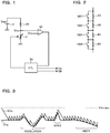
- Fig. 1 is a diagram showing a first configuration example of the voltage variation detection circuit.
- the voltage variation detection circuit shown in Fig. 1 includes a constant voltage source 1, a fixed resistor 2A, a variable resistor 3, a comparator 4A, and a controller 5A.
- a threshold voltage generation circuit arranged to generate a first threshold voltage V TH1 includes the constant voltage source 1, the fixed resistor 2A, and the variable resistor 3.
- the constant voltage source 1 generates a reference voltage V REF .
- a voltage dividing circuit composed of the fixed resistor 2A and the variable resistor 3 generates the first threshold voltage V TH1 , which is a partial voltage of the reference voltage V REF .
- the variable resistor 3 may be so structured that, for example as shown in Fig. 2 , resistors R1 to R4 are connected in series while switches SW1 to SW4 are connected in parallel to the resistors R1 to R4. With the structure shown in Fig. 2 , assuming that a resistance-value ratio of the resistors R1 to R4 is 2 0 :2 1 :2 2 :2 3 as an example, the resistance value of the variable resistor 3 can be changed in 2 4 steps at equal
- the comparator 4A compares a variation detection-target voltage V TG and the first threshold voltage V TH1 to each other. When the variation detection-target voltage V TG is equal to or more than the first threshold voltage V TH1 , the comparator 4A outputs a high-level signal. On the other hand, when the variation detection-target voltage V TG is less than the first threshold voltage V TH1 , the comparator 4A outputs a low-level signal.
- the controller 5A controls the above-described threshold voltage generation circuit based on output of the comparator 4A. More specifically, the controller 5A controls resistance value of the variable resistor 3. In addition, it is also allowable that the constant voltage source 1 is changed to a variable voltage source, where the controller 5A controls output voltage of the variable voltage source.
- the threshold voltage generation circuit repeats the following operations including:
- the threshold voltage generation circuit sets the first threshold voltage V TH1 to a maximum (see V TH1_MAX in Fig. 3 ) instead of increasing the first threshold voltage V TH1 by specified steps.
- the first threshold voltage V TH1 varies as shown in Fig. 3 .
- the first threshold voltage V TH1 is charted seemingly in a continuously-varying way in Fig. 3 for convenience' sake, the first threshold voltage V TH1 actually changes stepwise as apparent from the above description.
- the controller 5A detects variations of the variation detection-target voltage V TG based on control results at time points of transition of the variation detection-target voltage V TG to the first threshold voltage V TH1 or more (see black dots in Fig. 3 ). That is, from control results (resistance values of the variable resistor 3) at time points of transition of the variation detection-target voltage V TG to the first threshold voltage V TH1 or more (see black dots in Fig. 3 ), the controller 5A detects values of the variation detection-target voltage V TG at the time points, respectively, of transition of the variation detection-target voltage V TG to the first threshold voltage V TH1 or more (see black dots in Fig. 3 ), thereby detecting variations of the variation detection-target voltage V TG .
- the controller 5A outputs a notification signal SA for notification of a detection result as to variations of the variation detection-target voltage V TG .
- the notification signal SA may be multi-valued or a plurality of types of notification signals SA may be provided.
- the controller 5A may also be so arranged as to determine extremal values of the variation detection-target voltage V TG , as an example, and detect an oscillation of the variation detection-target voltage V TG on condition that a group of determined extremal values has a specified periodicity.
- the controller 5A may still also be so arranged as to determine a latest average value of the variation detection-target voltage V TG in a specified time period, as an example, and detect a spike of the variation detection-target voltage V TG on condition that a difference between the latest average value and a latest value of the variation detection-target voltage V TG is more than a specified extent.
- the controller 5A may yet also be so arranged as to determine both a latest average value of the variation detection-target voltage V TG in a specified time period and a second latest average value of the variation detection-target voltage V TG in the specified time period, as an example, and detect a drift of the variation detection-target voltage V TG on condition that a difference between the latest average value and the second latest average value is more than a specified extent.
- the controller 5A detects that the variation detection-target voltage V TG has become an overvoltage. Upon detection that the variation detection-target voltage V TG has become an overvoltage, the controller 5A outputs an overvoltage notification signal SB for notifying that the variation detection-target voltage V TG has become an overvoltage. Therefore, the voltage variation detection circuit shown in Fig. 1 serves also as an overvoltage detection circuit.
- the above-described voltage variation detection circuit shown in Fig. 1 is enabled to detect variations in the variation detection-target voltage V TG with a structure involving no A/D converter.
- the threshold voltage generation circuit sets the first threshold voltage V TH1 to a maximum before performing again the operation of decreasing the first threshold voltage V TH1 stepwise.
- Fig. 4 is a diagram showing a second configuration example of the voltage variation detection circuit.
- the voltage variation detection circuit shown in Fig. 4 includes a constant voltage source 1, a variable resistor 3, a fixed resistor 2B, a comparator 4B, and a controller 5B. It is noted that the same component members in Fig. 4 as in Fig. 1 are designated by the same reference signs, and their detailed description is omitted.
- a threshold voltage generation circuit arranged to generate a second threshold voltage V TH2 includes the constant voltage source 1, the variable resistor 3, and the fixed resistor 2B.
- a voltage dividing circuit composed of the variable resistor 3 and the fixed resistor 2B generates a second threshold voltage V TH2 which is a partial voltage of a reference voltage V REF . The higher the resistance value of the variable resistor 3 becomes, the lower the second threshold voltage V TH2 becomes.
- the comparator 4B compares a variation detection-target voltage V TG and the second threshold voltage V TH2 to each other. When the variation detection-target voltage V TG is equal to or less than the second threshold voltage V TH2 , the comparator 4B outputs a high-level signal. On the other hand, when the variation detection-target voltage V TG is higher than the second threshold voltage V TH2 , the comparator 4B outputs a low-level signal.
- the controller 5B controls the above-described threshold voltage generation circuit based on output of the comparator 4B. More specifically, the controller 5B controls resistance value of the variable resistor 3. In addition, it is also allowable that the constant voltage source 1 is changed to a variable voltage source, where the controller 5B controls output voltage of the variable voltage source.
- the threshold voltage generation circuit repeats the following operations including:
- the threshold voltage generation circuit sets the second threshold voltage V TH2 to a minimum (see V TH2_MIN in Fig. 5 ) instead of decreasing the second threshold voltage V TH2 by specified steps.
- the second threshold voltage V TH2 varies as shown in Fig. 5 .
- the second threshold voltage V TH2 is charted seemingly in a continuously-varying way in Fig. 5 for convenience' sake, the second threshold voltage V TH2 actually changes stepwise as apparent from the above description.
- the controller 5B detects a variation of the variation detection-target voltage V TG based on control results at time points when the variation detection-target voltage V TG comes to the second threshold voltage V TH2 or less (see black dots in Fig. 5 ). That is, from control results (resistance values of the variable resistor 3) at time points of transition of the variation detection-target voltage V TG to the second threshold voltage V TH2 or less (see black dots in Fig. 5 ), the controller 5B detects values of the variation detection-target voltage V TG at the time points, respectively, of transition of the variation detection-target voltage V TG to the second threshold voltage V TH2 or less (see black dots in Fig. 5 ), thereby detecting variations of the variation detection-target voltage V TG .
- the controller 5B outputs a notification signal SA for notification of a detection result as to variations of the variation detection-target voltage V TG .
- the notification signal SA may be multi-valued or a plurality of types of notification signals SA may be provided.
- the controller 5B may also be so arranged as to detect at least one of an oscillation of the variation detection-target voltage V TG , a spike of the variation detection-target voltage V TG , and a drift of the variation detection-target voltage V TG .
- the controller 5B detects that the variation detection-target voltage V TG has become a low voltage. Upon detection that the variation detection-target voltage V TG has become a low voltage, the controller 5B outputs a low-voltage notification signal SC for notifying that the variation detection-target voltage V TG has become a low voltage. Therefore, the voltage variation detection circuit shown in Fig. 4 serves also as a low-voltage detection circuit.
- the above-described voltage variation detection circuit shown in Fig. 4 is enabled to detect variations in the variation detection-target voltage V TG with a structure involving no A/D converter.
- the threshold voltage generation circuit sets the second threshold voltage V TH2 to a minimum before performing the operation of again increasing the second threshold voltage V TH2 stepwise.
- Fig. 6 is a diagram showing a third configuration example of the voltage variation detection circuit.
- the voltage variation detection circuit shown in Fig. 6 includes a constant voltage source 1, fixed resistors 2A and 2B, a variable resistor 3, comparators 4A and 4B, and a controller 5C. It is noted that the same component members in Fig. 6 as in Figs. 1 and 4 are designated by the same reference signs, and their detailed description is omitted.
- a threshold voltage generation circuit arranged to generate a first threshold voltage V TH1 and a second threshold voltage V TH2 includes the constant voltage source 1, the fixed resistor 2A, the variable resistor 3, and the fixed resistor 2B.
- a voltage dividing circuit composed of the fixed resistor 2A, the variable resistor 3 and the fixed resistor 2B generates a first threshold voltage V TH1 and a second threshold voltage V TH2 which are partial voltages of a reference voltage V REF .
- the reference voltage V REF is applied to a first terminal of the fixed resistor 2A, and a first terminal of the variable resistor 3 is connected to a second terminal of the fixed resistor 2A.
- a first terminal of the fixed resistor 2B is connected to a second terminal of the variable resistor 3, and a second terminal of the fixed resistor 2B is grounded.
- the first threshold voltage V TH1 is developed to a connection node between the fixed resistor 2A and the variable resistor 3
- the second threshold voltage V TH2 is developed to a connection node between the variable resistor 3 and the fixed resistor 2B.
- the controller 5C controls the above-described threshold voltage generation circuit based on output of the comparator 4A and output of the comparator 4B. More specifically, the controller 5C controls resistance value of the variable resistor 3.
- the threshold voltage generation circuit repeats the following operations including:
- the threshold voltage generation circuit sets the first threshold voltage V TH1 to a maximum instead of increasing the first threshold voltage V TH1 by specified steps.
- the threshold voltage generation circuit sets the second threshold voltage V TH2 to a minimum instead of decreasing the second threshold voltage V TH2 by specified steps.
- the first threshold voltage V TH1 and the second threshold voltage V TH2 vary as shown in Fig. 7 .
- the first threshold voltage V TH1 and the second threshold voltage V TH2 are charted seemingly in a continuously-varying way in Fig. 7 for convenience' sake, the first threshold voltage V TH1 and the second threshold voltage V TH2 actually change stepwise as apparent from the above description.
- the controller 5C detects a variation of the variation detection-target voltage V TG based on control results at time points when the variation detection-target voltage V TG comes to the first threshold voltage V TH1 or more or to the second threshold voltage V TH2 or less (see black dots in Fig. 7 ). That is, from control results (resistance values of the variable resistor 3) at time points of transition of the variation detection-target voltage V TG to the first threshold voltage V TH1 or more or to the second threshold voltage V TH2 or less (see black dots in Fig.
- the controller 5C detects values of the variation detection-target voltage V TG at the time points, respectively, of transition of the variation detection-target voltage V TG to the first threshold voltage V TH1 or more or to the second threshold voltage V TH2 or less (see black dots in Fig. 7 ), thereby detecting variations of the variation detection-target voltage V TG .
- the controller 5C outputs a notification signal SA for notification of a detection result as to variations of the variation detection-target voltage V TG .
- the notification signal SA may be multi-valued or a plurality of types of notification signals SA may be provided.
- the controller 5C may also be so arranged as to detect at least one of an oscillation of the variation detection-target voltage V TG , a spike of the variation detection-target voltage V TG , and a drift of the variation detection-target voltage V TG .
- the controller 5C detects that the variation detection-target voltage V TG has become an overvoltage. Upon detection that the variation detection-target voltage V TG has become an overvoltage, the controller 5C outputs an overvoltage notification signal SB for notifying that the variation detection-target voltage V TG has become an overvoltage. Therefore, the voltage variation detection circuit shown in Fig. 6 serves also as an overvoltage detection circuit.
- the controller 5C detects that the variation detection-target voltage V TG has become a low voltage. Upon detection that the variation detection-target voltage V TG has become a low voltage, the controller 5C outputs a low-voltage notification signal SC for notifying that the variation detection-target voltage V TG has become a low voltage. Therefore, the voltage variation detection circuit shown in Fig. 6 serves also as a low-voltage detection circuit.
- the above-described voltage variation detection circuit shown in Fig. 6 is enabled to detect variations in the variation detection-target voltage V TG with a structure involving no A/D converter.
- Fig. 8 is a diagram showing a configuration example of a switching power unit including the voltage variation detection circuit.
- Fig. 9 is a diagram showing a configuration example of an LDO (Low Drop-Out regulator) including the voltage variation detection circuit.
- LDO Low Drop-Out regulator
- the switching power unit shown in Fig. 8 includes a switching power IC 100.
- the switching power IC 100 is a semiconductor integrated circuit device in which integrated are a regulation voltage generator 101, a constant voltage source 102, an error amplifier 103, an oscillation circuit 104, a slope voltage generator 105, a PWM comparator 106, a driver 107, and voltage variation detection circuits 108 and 109. Also, the switching power IC 100 has external terminals T101 to T105 for establishment of electrical connections with the external.
- NMOS transistor Q101 N-channel type MOS field-effect transistor Q101
- diode D101 diode D101
- resistors R101 to R103 resistors
- a power supply voltage Vcc is applied to the external terminal T101, and the external terminal T102 is grounded.
- the power supply voltage Vcc is applied to a first terminal of the coil L101, and a second terminal of the coil L101 is connected to a drain of the NMOS transistor Q101 and an anode of the diode D101.
- a source of the NMOS transistor Q101 is grounded via the resistor R101 for current detection.
- a gate of the NMOS transistor Q101 is connected to the external terminal T103, and the source of the NMOS transistor Q101 is connected to the external terminal T104.
- a cathode of the diode D101 is connected to a first terminal of the output capacitor C101 and a first terminal of the resistor R102.
- a second terminal of the output capacitor C101 is grounded.
- a second terminal of the resistor R102 is connected to the external terminal T105 and a first terminal of the resistor R103.
- a second terminal of the resistor R103 is grounded.
- a voltage dividing circuit composed of the resistors R102 and R103 generates a feedback voltage V FB by dividing an output voltage V OUT of the switching power unit, and feeds the feedback voltage V FB to the external terminal T105.
- the regulation voltage generator 101 generates a regulation voltage V REG from the power supply voltage Vcc applied to the external terminal T101.
- the regulation voltage V REG is used as a drive voltage for other circuit blocks.
- the constant voltage source 102 generates a reference voltage V REF .
- the error amplifier 103 generates an error voltage V ERR responsive to a difference between the reference voltage V REF applied to its noninverting input terminal (+) and the feedback voltage V FB applied to its inverting input terminal (-).
- the oscillation circuit 104 generates a clock signal CK.
- the slope voltage generator 105 generates a chopping-wave or sawtooth-wave shaped slope voltage V SLP responsive to a current detected by the resistor R101 with use of the clock signal CK.
- the PWM comparator 106 compares an error voltage V ERR applied to the inverting input terminal (-) and a slope voltage V SLP applied to the noninverting input terminal (+) to each other to generate a PWM signal S1 responsive to a comparison result.
- the driver 107 generates a gate signal of the NMOS transistor Q101 in response to the PWM signal S1, and outputs the gate signal to the external terminal T103.
- the NMOS transistor Q101 is on/off controlled by the gate signal outputted from the external terminal T103.
- the voltage variation detection circuit 108 detects a variation of the power supply voltage Vcc. For example, assuming that the power supply voltage Vcc is obtained from output voltage of a battery, for fear of decline in the power supply voltage Vcc, the voltage variation detection circuit shown in Fig. 4 may appropriately be used as the voltage variation detection circuit 108.
- the voltage variation detection circuit 109 detects a variation of the feedback voltage V FB . Because of possibilities that the feedback voltage V FB may be an overvoltage or a low voltage, the voltage variation detection circuit shown in Fig. 6 may appropriately be used as the voltage variation detection circuit 109.
- Notification signals outputted from the voltage variation detection circuits 108 and 109 are usable, for example, as signals for instructing operation halts of the PWM comparator 106, the driver 107 and the like. Further, external terminals for externally outputting notification signals outputted from the voltage variation detection circuits 108 and 109 may be provided in the switching power IC 100, and notification signals outputted from the voltage variation detection circuits 108 and 109 may be outputted outside the switching power IC 100.
- the voltage variation detection circuit 109 has a constant voltage source for generating the reference voltage V REF , it is unadvisable to make shared use between the constant voltage source of the voltage variation detection circuit 109 and the constant voltage source 102. As to the reason of this, providing the constant voltage source of the voltage variation detection circuit 109 and the constant voltage source 102 as circuits independent of each other allows the voltage variation detection circuit 109 to detect a variation of the feedback voltage V FB even when the feedback voltage V FB has varied due to an abnormality of the constant voltage source 102.
- the constant voltage source of the voltage variation detection circuit 108 may be provided by shared use of, for example, the constant voltage source of the voltage variation detection circuit 109.
- the LDO shown in Fig. 9 includes an LDO IC 200.
- the LDO IC 200 is a semiconductor integrated circuit device in which integrated are a regulation voltage generator 201, a constant voltage source 202, an error amplifier 203, a P-channel type MOS field-effect transistor Q201 (hereinafter, referred to as PMOS transistor Q201), resistors R201 and R202, and a voltage variation detection circuit 204. Also, the LDO IC 200 has external terminals T201 to T203 for establishment of electrical connections with the external.
- An output capacitor C201 is externally connected to the LDO IC 200.
- a power supply voltage Vcc is applied to the external terminal T201, and the external terminal T202 is grounded.
- a first terminal of the output capacitor C201 is connected to the external terminal T203, and a second terminal of the output capacitor C201 is grounded.
- the regulation voltage generator 201 generates a regulation voltage V REG from the power supply voltage Vcc applied to the external terminal T201.
- the regulation voltage V REG is used as a drive voltage for other circuit blocks.
- the PMOS transistor Q201 generates an output voltage V OUT by stepping down the power supply voltage Vcc and outputs the output voltage V OUT to the external terminal T203.
- a voltage dividing circuit composed of the resistors R201 and R202 generates a feedback voltage V FB by dividing the output voltage V OUT .
- the constant voltage source 202 generates a reference voltage V REF .
- the error amplifier 203 generates an error voltage V ERR responsive to a difference between the feedback voltage V FB applied to the noninverting input terminal (+) and the reference voltage V REF applied to the inverting input terminal (-).
- the error voltage V ERR is fed to the gate of the PMOS transistor Q201. Therefore, on-resistance of the PMOS transistor Q201 is regulated by the error voltage V ERR .
- the voltage variation detection circuit 204 detects a variation of the output voltage V OUT .
- the voltage variation detection circuit shown in Fig. 1 may appropriately be used as the voltage variation detection circuit 204.
- a notification signal outputted from the voltage variation detection circuit 204 is usable, for example, as a signal for instructing an operation halt of the error amplifier 203. Further, an external terminal for externally outputting a notification signal outputted from the voltage variation detection circuit 204 may be provided in the LDO IC 200, and a notification signal outputted from the voltage variation detection circuit 204 may be outputted outside the LDO IC 200.
- the voltage variation detection circuit 204 has a constant voltage source for generating the reference voltage V REF , it is unadvisable to make shared use between the constant voltage source of the voltage variation detection circuit 204 and the constant voltage source 202. As to the reason of this, providing the constant voltage source of the voltage variation detection circuit 204 and the constant voltage source 202 as circuits independent of each other allows the voltage variation detection circuit 204 to detect a variation of the output voltage V OUT even when the output voltage V OUT has varied due to an abnormality of the constant voltage source 202.
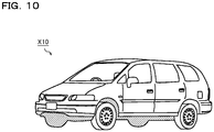
- the above-described power unit is mounted, for example, on a vehicle X10 shown in Fig. 10 .
- the switching power unit shown in Fig. 8 for example, is usable as a power unit for feeding power supply voltage to the MCU (Micro Control Unit) mounted on the vehicle X10.
- the LDO shown in Fig. 9 for example, is usable as the power unit for feeding power supply voltage to a camera and a sensor for use in advanced operation aid systems mounted on the vehicle X10.
- the output stage of the switching power circuit is provided as a step-up type one as an example in Fig. 8
- the output stage is not limited to this and may be easily adapted to any one of step-down type, step-up/down type, and SEPIC type. That is, the foregoing embodiments should be construed as not being limitative but being an exemplification at all points.
- the technical scope of the present invention should be defined not by the above description of the embodiments but by the appended claims, including all changes and modifications equivalent in sense and range to the claims.
- a voltage variation detection circuit includes: a threshold voltage generation circuit arranged to generate a threshold voltage; a comparator arranged to compare a variation detection-target voltage and the threshold voltage to each other; and a controller arranged to control the threshold voltage generation circuit based on output of the comparator, wherein the controller controls the threshold voltage generation circuit in such fashion that the threshold voltage generation circuit repeats operations of: decreasing the threshold voltage stepwise; when the variation detection-target voltage has come to the threshold voltage or more, first increasing the threshold voltage by specified steps and then again decreasing the threshold voltage stepwise; and when the variation detection-target voltage has come to the threshold voltage or more, increasing the threshold voltage by specified steps, and wherein the controller detects a variation of the variation detection-target voltage based on control results at time points when the variation detection-target voltage comes to the threshold voltage or more.
- the controller may set the threshold voltage to a maximum before again decreasing the threshold voltage stepwise (second configuration).
- a voltage variation detection circuit includes: a threshold voltage generation circuit arranged to generate a threshold voltage; a comparator arranged to compare a variation detection-target voltage and the threshold voltage to each other; and a controller arranged to control the threshold voltage generation circuit based on output of the comparator, wherein the controller controls the threshold voltage generation circuit in such fashion that the threshold voltage generation circuit repeats operations of: increasing the threshold voltage stepwise; when the variation detection-target voltage has come to the threshold voltage or less, first decreasing the threshold voltage by specified steps and then again increasing the threshold voltage stepwise; and when the variation detection-target voltage has come to the threshold voltage or less, decreasing the threshold voltage by specified steps, and wherein the controller detects a variation of the variation detection-target voltage based on control results at time points when the variation detection-target voltage comes to the threshold voltage or less.
- the controller may set the threshold voltage to a minimum before again increasing the threshold voltage stepwise (fourth configuration).
- a voltage variation detection circuit in a fifth configuration described hereinabove includes: a threshold voltage generation circuit arranged to generate a first threshold voltage and a second threshold voltage lower than the first threshold voltage; a first comparator arranged to compare a variation detection-target voltage and the first threshold voltage to each other; a second comparator arranged to compare the variation detection-target voltage and the second threshold voltage to each other; and a controller arranged to control the threshold voltage generation circuit based on output of the first comparator and output of the second comparator, wherein the controller controls the threshold voltage generation circuit in such fashion that the threshold voltage generation circuit repeats operations of: decreasing the first threshold voltage stepwise and increasing the second threshold voltage stepwise; when the variation detection-target voltage has come to the first threshold voltage or more or to the second threshold voltage or less, first increasing the first threshold voltage by specified steps and decreasing the second threshold voltage by specified steps and then again decreasing the first threshold voltage stepwise and increasing the second threshold voltage stepwise; and when the variation detection-target voltage has come to the threshold voltage or more or to the second threshold voltage or less, increasing the first
- the threshold voltage generation circuit may include: a first fixed resistor; a variable resistor whose resistance value is variable stepwise; and a second fixed resistor, wherein a reference voltage is applied to a first terminal of the first fixed resistor, a first terminal of the variable resistor is connected to a second terminal of the first fixed resistor, a first terminal of the second fixed resistor is connected to a second terminal of the variable resistor, a second terminal of the second fixed resistor is grounded, and the first threshold voltage is developed to a connection node between the first fixed resistor and the variable resistor while the second threshold voltage is developed to a connection node between the variable resistor and the second fixed resistor (sixth configuration).
- the controller may detect that the variation detection-target voltage has become an overvoltage on condition that the variation detection-target voltage is equal to or more than the first threshold voltage when the first threshold voltage is at a maximum (seventh configuration).
- the controller may detect that the variation detection-target voltage has become a low voltage on condition that the variation detection-target voltage is equal to or less than the second threshold voltage when the second threshold voltage is at a minimum (eighth configuration).
- the controller may detect at least one of an oscillation of the variation detection-target voltage, a spike of the variation detection-target voltage, and a drift of the variation detection-target voltage (ninth configuration).
- a semiconductor integrated circuit described hereinabove includes: the voltage variation detection circuit according to any one of the first to ninth configurations; and at least part of a voltage generation circuit arranged to generate the variation detection-target voltage (tenth configuration).
- a vehicle described hereinabove includes: the semiconductor integrated circuit according to the tenth configuration (eleventh configuration).
Landscapes
- Physics & Mathematics (AREA)
- Nonlinear Science (AREA)
- General Physics & Mathematics (AREA)
- Measurement Of Current Or Voltage (AREA)
- Dc-Dc Converters (AREA)
Applications Claiming Priority (1)
| Application Number | Priority Date | Filing Date | Title |
|---|---|---|---|
| JP2016239612A JP6868381B2 (ja) | 2016-12-09 | 2016-12-09 | 電圧変動検知回路、半導体集積回路、車両 |
Publications (2)
| Publication Number | Publication Date |
|---|---|
| EP3333581A1 true EP3333581A1 (de) | 2018-06-13 |
| EP3333581B1 EP3333581B1 (de) | 2020-11-18 |
Family
ID=60661783
Family Applications (1)
| Application Number | Title | Priority Date | Filing Date |
|---|---|---|---|
| EP17205996.6A Active EP3333581B1 (de) | 2016-12-09 | 2017-12-07 | Spannungsvariationserfassungsschaltung, integrierte halbleiterschaltung und fahrzeug |
Country Status (3)
| Country | Link |
|---|---|
| US (1) | US10830798B2 (de) |
| EP (1) | EP3333581B1 (de) |
| JP (1) | JP6868381B2 (de) |
Cited By (1)
| Publication number | Priority date | Publication date | Assignee | Title |
|---|---|---|---|---|
| US20210034089A1 (en) * | 2015-09-04 | 2021-02-04 | Texas Instruments Incorporated | Voltage regulator wake-up |
Families Citing this family (3)
| Publication number | Priority date | Publication date | Assignee | Title |
|---|---|---|---|---|
| DE102015225804A1 (de) * | 2015-12-17 | 2017-06-22 | Dialog Semiconductor (Uk) Limited | Spannungsregler mit Impedanzkompensation |
| CN115308467B (zh) * | 2021-05-07 | 2025-12-23 | 脸萌有限公司 | 集成电路内部电压检测电路、检测方法以及集成电路 |
| CN115902416B (zh) * | 2022-10-31 | 2026-04-03 | 北京角动力技术有限公司 | 一种电路的信号监测装置 |
Citations (11)
| Publication number | Priority date | Publication date | Assignee | Title |
|---|---|---|---|---|
| JP2005326313A (ja) | 2004-05-14 | 2005-11-24 | Osaka Gas Co Ltd | 電圧変動検知回路 |
| US20090267821A1 (en) * | 2008-04-24 | 2009-10-29 | Erik Chmelar | Analog-to-Digital Converter |
| US20090303096A1 (en) * | 2008-06-06 | 2009-12-10 | Lsi Corporation | Systems and methods for analog to digital conversion |
| EP2290823A1 (de) * | 2008-06-06 | 2011-03-02 | Sony Corporation | Festkörperabbildungsvorrichtung, abbildungsvorrichtung, elektronisches gerät, ad-wandler und ad-umwandlungsverfahren |
| US20120008028A1 (en) * | 2010-07-08 | 2012-01-12 | Kabushiki Kaisha Toshiba | Solid state imaging device |
| EP2555509A1 (de) * | 2011-08-05 | 2013-02-06 | Canon Kabushiki Kaisha | Bildaufnahmevorrichtung mit Sägezahnverfahren AD Umsetzer |
| WO2013042918A1 (ko) * | 2011-09-19 | 2013-03-28 | 동국대학교 산학협력단 | 복수 개의 램프 신호를 사용하는 다중 스텝 구조의 adc 및 이를 이용한 아날로그-디지털 변환 방법 |
| US20140160331A1 (en) * | 2011-08-30 | 2014-06-12 | Panasonic Corporation | Solid-state imaging device and imaging apparatus |
| US20140225760A1 (en) * | 2013-02-12 | 2014-08-14 | Omnivision Technologies, Inc. | Adaptive multiple conversion ramp analog-to-digital converter |
| US20140240568A1 (en) * | 2013-02-27 | 2014-08-28 | Sony Corporation | Electronic apparatus, control method, and image sensor |
| CN103532552B (zh) * | 2013-10-10 | 2016-08-24 | 中国科学院微电子研究所 | 一种随机采样斜率模数转换器 |
Family Cites Families (12)
| Publication number | Priority date | Publication date | Assignee | Title |
|---|---|---|---|---|
| JPS6130868U (ja) * | 1984-07-27 | 1986-02-24 | 横河電機株式会社 | 波高値測定装置 |
| JPH0412639A (ja) * | 1990-04-27 | 1992-01-17 | Hitachi Ltd | 車両用充電発電機 |
| JPH05215791A (ja) * | 1992-02-06 | 1993-08-24 | Rohm Co Ltd | 電圧低下検出回路 |
| JPH05335958A (ja) * | 1992-06-03 | 1993-12-17 | Matsushita Electric Ind Co Ltd | Ad変換装置 |
| JP4719190B2 (ja) * | 2006-07-06 | 2011-07-06 | 株式会社豊田中央研究所 | 2値化回路 |
| JP4853445B2 (ja) * | 2007-09-28 | 2012-01-11 | ソニー株式会社 | A/d変換回路、固体撮像素子、およびカメラシステム |
| KR101621244B1 (ko) * | 2009-02-13 | 2016-05-16 | 삼성전자주식회사 | 카운터 회로, 이를 포함하는 장치 및 카운팅 방법 |
| JP5432676B2 (ja) * | 2009-11-18 | 2014-03-05 | ルネサスエレクトロニクス株式会社 | マイクロコンピュータ、ヒステリシスコンパレータ回路、及び電圧監視装置 |
| JP5782238B2 (ja) * | 2010-07-30 | 2015-09-24 | ルネサスエレクトロニクス株式会社 | 電圧検出回路及びその制御方法 |
| KR101758090B1 (ko) * | 2010-12-06 | 2017-07-17 | 삼성전자주식회사 | 이미지 센서 및 이미지 센서를 포함하는 카메라 시스템 |
| US8754797B2 (en) * | 2012-08-30 | 2014-06-17 | Texas Instruments Incorporated | Asynchronous analog-to-digital converter having rate control |
| KR102000470B1 (ko) * | 2012-10-30 | 2019-07-16 | 삼성전자주식회사 | 듀티 정정 회로 및 이를 포함하는 시스템 |
-
2016
- 2016-12-09 JP JP2016239612A patent/JP6868381B2/ja active Active
-
2017
- 2017-12-07 US US15/834,241 patent/US10830798B2/en active Active
- 2017-12-07 EP EP17205996.6A patent/EP3333581B1/de active Active
Patent Citations (11)
| Publication number | Priority date | Publication date | Assignee | Title |
|---|---|---|---|---|
| JP2005326313A (ja) | 2004-05-14 | 2005-11-24 | Osaka Gas Co Ltd | 電圧変動検知回路 |
| US20090267821A1 (en) * | 2008-04-24 | 2009-10-29 | Erik Chmelar | Analog-to-Digital Converter |
| US20090303096A1 (en) * | 2008-06-06 | 2009-12-10 | Lsi Corporation | Systems and methods for analog to digital conversion |
| EP2290823A1 (de) * | 2008-06-06 | 2011-03-02 | Sony Corporation | Festkörperabbildungsvorrichtung, abbildungsvorrichtung, elektronisches gerät, ad-wandler und ad-umwandlungsverfahren |
| US20120008028A1 (en) * | 2010-07-08 | 2012-01-12 | Kabushiki Kaisha Toshiba | Solid state imaging device |
| EP2555509A1 (de) * | 2011-08-05 | 2013-02-06 | Canon Kabushiki Kaisha | Bildaufnahmevorrichtung mit Sägezahnverfahren AD Umsetzer |
| US20140160331A1 (en) * | 2011-08-30 | 2014-06-12 | Panasonic Corporation | Solid-state imaging device and imaging apparatus |
| WO2013042918A1 (ko) * | 2011-09-19 | 2013-03-28 | 동국대학교 산학협력단 | 복수 개의 램프 신호를 사용하는 다중 스텝 구조의 adc 및 이를 이용한 아날로그-디지털 변환 방법 |
| US20140225760A1 (en) * | 2013-02-12 | 2014-08-14 | Omnivision Technologies, Inc. | Adaptive multiple conversion ramp analog-to-digital converter |
| US20140240568A1 (en) * | 2013-02-27 | 2014-08-28 | Sony Corporation | Electronic apparatus, control method, and image sensor |
| CN103532552B (zh) * | 2013-10-10 | 2016-08-24 | 中国科学院微电子研究所 | 一种随机采样斜率模数转换器 |
Non-Patent Citations (2)
| Title |
|---|
| JIM: "Converters", 1 November 2012 (2012-11-01), pages 1 - 20, XP055468039, Retrieved from the Internet <URL:www.site.uottawa.ca/~rhabash/ELG3336LNConveters.pdf> * |
| MARK CHEN: "Analog-to-Digital Converters", 3 February 2010 (2010-02-03), pages 1 - 17, XP055468049, Retrieved from the Internet <URL:https://www.physics.queensu.ca/~phys352/lect08.pdf> * |
Cited By (2)
| Publication number | Priority date | Publication date | Assignee | Title |
|---|---|---|---|---|
| US20210034089A1 (en) * | 2015-09-04 | 2021-02-04 | Texas Instruments Incorporated | Voltage regulator wake-up |
| US12228954B2 (en) * | 2015-09-04 | 2025-02-18 | Texas Instruments Incorporated | Voltage regulator wake-up |
Also Published As
| Publication number | Publication date |
|---|---|
| JP6868381B2 (ja) | 2021-05-12 |
| JP2018096754A (ja) | 2018-06-21 |
| US20180164352A1 (en) | 2018-06-14 |
| US10830798B2 (en) | 2020-11-10 |
| EP3333581B1 (de) | 2020-11-18 |
Similar Documents
| Publication | Publication Date | Title |
|---|---|---|
| US9831780B2 (en) | Buck-boost converter and method for controlling buck-boost converter | |
| CN107305400B (zh) | 基准电压产生电路以及具有该电路的dcdc转换器 | |
| US9293990B2 (en) | Switching regulator and electronic apparatus | |
| US8525580B2 (en) | Semiconductor circuit and constant voltage regulator employing same | |
| US10830798B2 (en) | Voltage variation detection circuit, semiconductor integrated circuit, and vehicle | |
| EP1690331B1 (de) | Leistungsschaltung und verfahren zur vergrösserung der ausgangsspannung einer leistungsschaltung | |
| US9030184B2 (en) | DC-DC converter and voltage conversion method thereof | |
| CN107305402B (zh) | 带隙基准电路以及具有该带隙基准电路的dcdc转换器 | |
| JP5640562B2 (ja) | 多出力電源装置 | |
| CN104135151B (zh) | 直流转直流转换控制器 | |
| US10185338B1 (en) | Digital low drop-out (LDO) voltage regulator with analog-assisted dynamic reference correction | |
| JP2011223829A (ja) | 負電圧チャージポンプ回路の制御回路および負電圧チャージポンプ回路、ならびにそれらを用いた電子機器およびオーディオシステム | |
| KR101904595B1 (ko) | 연속적인 램프 업을 갖는 디지털 소프트 스타트 | |
| US12095252B2 (en) | Overcurrent protection circuit | |
| EP3206301A2 (de) | Oszillatorschaltung | |
| JP6224365B2 (ja) | 電源装置及び半導体装置 | |
| JP6382020B2 (ja) | ソフトスタート回路 | |
| US20140210439A1 (en) | Switching Regulator and Control Circuit Thereof | |
| JP2017139946A (ja) | スイッチング電源回路、負荷駆動装置、液晶表示装置 | |
| US8729878B2 (en) | Switching regulator control circuit and switching regulator | |
| KR20100005756A (ko) | 레플리카 부하를 이용한 저전압 강하 레귤레이터 | |
| EP2658108B1 (de) | Stromversorgungsschaltung | |
| JP5598507B2 (ja) | 電源装置 | |
| US11567520B2 (en) | Exponential-based slope compensation | |
| JP2009211210A (ja) | 電源回路装置および電子機器 |
Legal Events
| Date | Code | Title | Description |
|---|---|---|---|
| PUAI | Public reference made under article 153(3) epc to a published international application that has entered the european phase |
Free format text: ORIGINAL CODE: 0009012 |
|
| STAA | Information on the status of an ep patent application or granted ep patent |
Free format text: STATUS: REQUEST FOR EXAMINATION WAS MADE |
|
| 17P | Request for examination filed |
Effective date: 20180214 |
|
| AK | Designated contracting states |
Kind code of ref document: A1 Designated state(s): AL AT BE BG CH CY CZ DE DK EE ES FI FR GB GR HR HU IE IS IT LI LT LU LV MC MK MT NL NO PL PT RO RS SE SI SK SM TR |
|
| AX | Request for extension of the european patent |
Extension state: BA ME |
|
| GRAP | Despatch of communication of intention to grant a patent |
Free format text: ORIGINAL CODE: EPIDOSNIGR1 |
|
| STAA | Information on the status of an ep patent application or granted ep patent |
Free format text: STATUS: GRANT OF PATENT IS INTENDED |
|
| INTG | Intention to grant announced |
Effective date: 20200612 |
|
| GRAS | Grant fee paid |
Free format text: ORIGINAL CODE: EPIDOSNIGR3 |
|
| GRAA | (expected) grant |
Free format text: ORIGINAL CODE: 0009210 |
|
| STAA | Information on the status of an ep patent application or granted ep patent |
Free format text: STATUS: THE PATENT HAS BEEN GRANTED |
|
| AK | Designated contracting states |
Kind code of ref document: B1 Designated state(s): AL AT BE BG CH CY CZ DE DK EE ES FI FR GB GR HR HU IE IS IT LI LT LU LV MC MK MT NL NO PL PT RO RS SE SI SK SM TR |
|
| REG | Reference to a national code |
Ref country code: GB Ref legal event code: FG4D |
|
| REG | Reference to a national code |
Ref country code: CH Ref legal event code: EP |
|
| REG | Reference to a national code |
Ref country code: IE Ref legal event code: FG4D |
|
| REG | Reference to a national code |
Ref country code: DE Ref legal event code: R096 Ref document number: 602017027684 Country of ref document: DE |
|
| REG | Reference to a national code |
Ref country code: AT Ref legal event code: REF Ref document number: 1336339 Country of ref document: AT Kind code of ref document: T Effective date: 20201215 |
|
| REG | Reference to a national code |
Ref country code: AT Ref legal event code: MK05 Ref document number: 1336339 Country of ref document: AT Kind code of ref document: T Effective date: 20201118 |
|
| REG | Reference to a national code |
Ref country code: NL Ref legal event code: MP Effective date: 20201118 |
|
| PG25 | Lapsed in a contracting state [announced via postgrant information from national office to epo] |
Ref country code: RS Free format text: LAPSE BECAUSE OF FAILURE TO SUBMIT A TRANSLATION OF THE DESCRIPTION OR TO PAY THE FEE WITHIN THE PRESCRIBED TIME-LIMIT Effective date: 20201118 Ref country code: PT Free format text: LAPSE BECAUSE OF FAILURE TO SUBMIT A TRANSLATION OF THE DESCRIPTION OR TO PAY THE FEE WITHIN THE PRESCRIBED TIME-LIMIT Effective date: 20210318 Ref country code: NO Free format text: LAPSE BECAUSE OF FAILURE TO SUBMIT A TRANSLATION OF THE DESCRIPTION OR TO PAY THE FEE WITHIN THE PRESCRIBED TIME-LIMIT Effective date: 20210218 Ref country code: FI Free format text: LAPSE BECAUSE OF FAILURE TO SUBMIT A TRANSLATION OF THE DESCRIPTION OR TO PAY THE FEE WITHIN THE PRESCRIBED TIME-LIMIT Effective date: 20201118 Ref country code: GR Free format text: LAPSE BECAUSE OF FAILURE TO SUBMIT A TRANSLATION OF THE DESCRIPTION OR TO PAY THE FEE WITHIN THE PRESCRIBED TIME-LIMIT Effective date: 20210219 |
|
| PG25 | Lapsed in a contracting state [announced via postgrant information from national office to epo] |
Ref country code: BG Free format text: LAPSE BECAUSE OF FAILURE TO SUBMIT A TRANSLATION OF THE DESCRIPTION OR TO PAY THE FEE WITHIN THE PRESCRIBED TIME-LIMIT Effective date: 20210218 Ref country code: PL Free format text: LAPSE BECAUSE OF FAILURE TO SUBMIT A TRANSLATION OF THE DESCRIPTION OR TO PAY THE FEE WITHIN THE PRESCRIBED TIME-LIMIT Effective date: 20201118 Ref country code: LV Free format text: LAPSE BECAUSE OF FAILURE TO SUBMIT A TRANSLATION OF THE DESCRIPTION OR TO PAY THE FEE WITHIN THE PRESCRIBED TIME-LIMIT Effective date: 20201118 Ref country code: IS Free format text: LAPSE BECAUSE OF FAILURE TO SUBMIT A TRANSLATION OF THE DESCRIPTION OR TO PAY THE FEE WITHIN THE PRESCRIBED TIME-LIMIT Effective date: 20210318 Ref country code: AT Free format text: LAPSE BECAUSE OF FAILURE TO SUBMIT A TRANSLATION OF THE DESCRIPTION OR TO PAY THE FEE WITHIN THE PRESCRIBED TIME-LIMIT Effective date: 20201118 Ref country code: SE Free format text: LAPSE BECAUSE OF FAILURE TO SUBMIT A TRANSLATION OF THE DESCRIPTION OR TO PAY THE FEE WITHIN THE PRESCRIBED TIME-LIMIT Effective date: 20201118 |
|
| REG | Reference to a national code |
Ref country code: LT Ref legal event code: MG9D |
|
| PG25 | Lapsed in a contracting state [announced via postgrant information from national office to epo] |
Ref country code: HR Free format text: LAPSE BECAUSE OF FAILURE TO SUBMIT A TRANSLATION OF THE DESCRIPTION OR TO PAY THE FEE WITHIN THE PRESCRIBED TIME-LIMIT Effective date: 20201118 |
|
| PG25 | Lapsed in a contracting state [announced via postgrant information from national office to epo] |
Ref country code: SK Free format text: LAPSE BECAUSE OF FAILURE TO SUBMIT A TRANSLATION OF THE DESCRIPTION OR TO PAY THE FEE WITHIN THE PRESCRIBED TIME-LIMIT Effective date: 20201118 Ref country code: RO Free format text: LAPSE BECAUSE OF FAILURE TO SUBMIT A TRANSLATION OF THE DESCRIPTION OR TO PAY THE FEE WITHIN THE PRESCRIBED TIME-LIMIT Effective date: 20201118 Ref country code: SM Free format text: LAPSE BECAUSE OF FAILURE TO SUBMIT A TRANSLATION OF THE DESCRIPTION OR TO PAY THE FEE WITHIN THE PRESCRIBED TIME-LIMIT Effective date: 20201118 Ref country code: EE Free format text: LAPSE BECAUSE OF FAILURE TO SUBMIT A TRANSLATION OF THE DESCRIPTION OR TO PAY THE FEE WITHIN THE PRESCRIBED TIME-LIMIT Effective date: 20201118 Ref country code: CZ Free format text: LAPSE BECAUSE OF FAILURE TO SUBMIT A TRANSLATION OF THE DESCRIPTION OR TO PAY THE FEE WITHIN THE PRESCRIBED TIME-LIMIT Effective date: 20201118 Ref country code: LT Free format text: LAPSE BECAUSE OF FAILURE TO SUBMIT A TRANSLATION OF THE DESCRIPTION OR TO PAY THE FEE WITHIN THE PRESCRIBED TIME-LIMIT Effective date: 20201118 |
|
| REG | Reference to a national code |
Ref country code: CH Ref legal event code: PL |
|
| REG | Reference to a national code |
Ref country code: DE Ref legal event code: R097 Ref document number: 602017027684 Country of ref document: DE |
|
| PG25 | Lapsed in a contracting state [announced via postgrant information from national office to epo] |
Ref country code: DK Free format text: LAPSE BECAUSE OF FAILURE TO SUBMIT A TRANSLATION OF THE DESCRIPTION OR TO PAY THE FEE WITHIN THE PRESCRIBED TIME-LIMIT Effective date: 20201118 Ref country code: MC Free format text: LAPSE BECAUSE OF FAILURE TO SUBMIT A TRANSLATION OF THE DESCRIPTION OR TO PAY THE FEE WITHIN THE PRESCRIBED TIME-LIMIT Effective date: 20201118 |
|
| REG | Reference to a national code |
Ref country code: BE Ref legal event code: MM Effective date: 20201231 |
|
| PLBE | No opposition filed within time limit |
Free format text: ORIGINAL CODE: 0009261 |
|
| STAA | Information on the status of an ep patent application or granted ep patent |
Free format text: STATUS: NO OPPOSITION FILED WITHIN TIME LIMIT |
|
| 26N | No opposition filed |
Effective date: 20210819 |
|
| PG25 | Lapsed in a contracting state [announced via postgrant information from national office to epo] |
Ref country code: NL Free format text: LAPSE BECAUSE OF FAILURE TO SUBMIT A TRANSLATION OF THE DESCRIPTION OR TO PAY THE FEE WITHIN THE PRESCRIBED TIME-LIMIT Effective date: 20201118 Ref country code: AL Free format text: LAPSE BECAUSE OF FAILURE TO SUBMIT A TRANSLATION OF THE DESCRIPTION OR TO PAY THE FEE WITHIN THE PRESCRIBED TIME-LIMIT Effective date: 20201118 Ref country code: IE Free format text: LAPSE BECAUSE OF NON-PAYMENT OF DUE FEES Effective date: 20201207 Ref country code: FR Free format text: LAPSE BECAUSE OF NON-PAYMENT OF DUE FEES Effective date: 20210118 Ref country code: IT Free format text: LAPSE BECAUSE OF FAILURE TO SUBMIT A TRANSLATION OF THE DESCRIPTION OR TO PAY THE FEE WITHIN THE PRESCRIBED TIME-LIMIT Effective date: 20201118 Ref country code: LU Free format text: LAPSE BECAUSE OF NON-PAYMENT OF DUE FEES Effective date: 20201207 |
|
| PG25 | Lapsed in a contracting state [announced via postgrant information from national office to epo] |
Ref country code: LI Free format text: LAPSE BECAUSE OF NON-PAYMENT OF DUE FEES Effective date: 20201231 Ref country code: SI Free format text: LAPSE BECAUSE OF FAILURE TO SUBMIT A TRANSLATION OF THE DESCRIPTION OR TO PAY THE FEE WITHIN THE PRESCRIBED TIME-LIMIT Effective date: 20201118 Ref country code: CH Free format text: LAPSE BECAUSE OF NON-PAYMENT OF DUE FEES Effective date: 20201231 |
|
| PG25 | Lapsed in a contracting state [announced via postgrant information from national office to epo] |
Ref country code: ES Free format text: LAPSE BECAUSE OF FAILURE TO SUBMIT A TRANSLATION OF THE DESCRIPTION OR TO PAY THE FEE WITHIN THE PRESCRIBED TIME-LIMIT Effective date: 20201118 |
|
| PG25 | Lapsed in a contracting state [announced via postgrant information from national office to epo] |
Ref country code: IS Free format text: LAPSE BECAUSE OF FAILURE TO SUBMIT A TRANSLATION OF THE DESCRIPTION OR TO PAY THE FEE WITHIN THE PRESCRIBED TIME-LIMIT Effective date: 20210318 Ref country code: TR Free format text: LAPSE BECAUSE OF FAILURE TO SUBMIT A TRANSLATION OF THE DESCRIPTION OR TO PAY THE FEE WITHIN THE PRESCRIBED TIME-LIMIT Effective date: 20201118 Ref country code: MT Free format text: LAPSE BECAUSE OF FAILURE TO SUBMIT A TRANSLATION OF THE DESCRIPTION OR TO PAY THE FEE WITHIN THE PRESCRIBED TIME-LIMIT Effective date: 20201118 Ref country code: CY Free format text: LAPSE BECAUSE OF FAILURE TO SUBMIT A TRANSLATION OF THE DESCRIPTION OR TO PAY THE FEE WITHIN THE PRESCRIBED TIME-LIMIT Effective date: 20201118 |
|
| PG25 | Lapsed in a contracting state [announced via postgrant information from national office to epo] |
Ref country code: MK Free format text: LAPSE BECAUSE OF FAILURE TO SUBMIT A TRANSLATION OF THE DESCRIPTION OR TO PAY THE FEE WITHIN THE PRESCRIBED TIME-LIMIT Effective date: 20201118 |
|
| PG25 | Lapsed in a contracting state [announced via postgrant information from national office to epo] |
Ref country code: BE Free format text: LAPSE BECAUSE OF NON-PAYMENT OF DUE FEES Effective date: 20201231 |
|
| GBPC | Gb: european patent ceased through non-payment of renewal fee |
Effective date: 20211207 |
|
| PG25 | Lapsed in a contracting state [announced via postgrant information from national office to epo] |
Ref country code: GB Free format text: LAPSE BECAUSE OF NON-PAYMENT OF DUE FEES Effective date: 20211207 |
|
| P01 | Opt-out of the competence of the unified patent court (upc) registered |
Effective date: 20230512 |
|
| PGFP | Annual fee paid to national office [announced via postgrant information from national office to epo] |
Ref country code: DE Payment date: 20231031 Year of fee payment: 7 |
|
| REG | Reference to a national code |
Ref country code: DE Ref legal event code: R119 Ref document number: 602017027684 Country of ref document: DE |
|
| PG25 | Lapsed in a contracting state [announced via postgrant information from national office to epo] |
Ref country code: DE Free format text: LAPSE BECAUSE OF NON-PAYMENT OF DUE FEES Effective date: 20250701 |