EP3319231A1 - Verstärker - Google Patents
Verstärker Download PDFInfo
- Publication number
- EP3319231A1 EP3319231A1 EP16817484.5A EP16817484A EP3319231A1 EP 3319231 A1 EP3319231 A1 EP 3319231A1 EP 16817484 A EP16817484 A EP 16817484A EP 3319231 A1 EP3319231 A1 EP 3319231A1
- Authority
- EP
- European Patent Office
- Prior art keywords
- terminal
- transistor
- tia
- current source
- amplifier
- Prior art date
- Legal status (The legal status is an assumption and is not a legal conclusion. Google has not performed a legal analysis and makes no representation as to the accuracy of the status listed.)
- Withdrawn
Links
Images


Classifications
-
- H—ELECTRICITY
- H03—ELECTRONIC CIRCUITRY
- H03F—AMPLIFIERS
- H03F1/00—Details of amplifiers with only discharge tubes, only semiconductor devices or only unspecified devices as amplifying elements
- H03F1/26—Modifications of amplifiers to reduce influence of noise generated by amplifying elements
-
- H—ELECTRICITY
- H03—ELECTRONIC CIRCUITRY
- H03F—AMPLIFIERS
- H03F1/00—Details of amplifiers with only discharge tubes, only semiconductor devices or only unspecified devices as amplifying elements
- H03F1/08—Modifications of amplifiers to reduce detrimental influences of internal impedances of amplifying elements
- H03F1/083—Modifications of amplifiers to reduce detrimental influences of internal impedances of amplifying elements in transistor amplifiers
-
- H—ELECTRICITY
- H03—ELECTRONIC CIRCUITRY
- H03F—AMPLIFIERS
- H03F3/00—Amplifiers with only discharge tubes or only semiconductor devices as amplifying elements
- H03F3/04—Amplifiers with only discharge tubes or only semiconductor devices as amplifying elements with semiconductor devices only
- H03F3/08—Amplifiers with only discharge tubes or only semiconductor devices as amplifying elements with semiconductor devices only controlled by light
-
- H—ELECTRICITY
- H03—ELECTRONIC CIRCUITRY
- H03F—AMPLIFIERS
- H03F3/00—Amplifiers with only discharge tubes or only semiconductor devices as amplifying elements
- H03F3/20—Power amplifiers, e.g. Class B amplifiers, Class C amplifiers
- H03F3/21—Power amplifiers, e.g. Class B amplifiers, Class C amplifiers with semiconductor devices only
- H03F3/211—Power amplifiers, e.g. Class B amplifiers, Class C amplifiers with semiconductor devices only using a combination of several amplifiers
-
- H—ELECTRICITY
- H03—ELECTRONIC CIRCUITRY
- H03F—AMPLIFIERS
- H03F3/00—Amplifiers with only discharge tubes or only semiconductor devices as amplifying elements
- H03F3/34—Dc amplifiers in which all stages are dc-coupled
- H03F3/343—Dc amplifiers in which all stages are dc-coupled with semiconductor devices only
- H03F3/347—Dc amplifiers in which all stages are dc-coupled with semiconductor devices only in integrated circuits
-
- H—ELECTRICITY
- H04—ELECTRIC COMMUNICATION TECHNIQUE
- H04B—TRANSMISSION
- H04B10/00—Transmission systems employing electromagnetic waves other than radio-waves, e.g. infrared, visible or ultraviolet light, or employing corpuscular radiation, e.g. quantum communication
- H04B10/60—Receivers
- H04B10/66—Non-coherent receivers, e.g. using direct detection
- H04B10/69—Electrical arrangements in the receiver
- H04B10/693—Arrangements for optimizing the preamplifier in the receiver
-
- H—ELECTRICITY
- H03—ELECTRONIC CIRCUITRY
- H03F—AMPLIFIERS
- H03F2200/00—Indexing scheme relating to amplifiers
- H03F2200/294—Indexing scheme relating to amplifiers the amplifier being a low noise amplifier [LNA]
-
- H—ELECTRICITY
- H03—ELECTRONIC CIRCUITRY
- H03F—AMPLIFIERS
- H03F2200/00—Indexing scheme relating to amplifiers
- H03F2200/72—Indexing scheme relating to amplifiers the amplifier stage being a common gate configuration MOSFET
Definitions
- the present invention relates to an amplifier. More particularly, the invention relates to an amplifier applied to a transimpedance amplifier to covert a current signal converted from an optical signal by a photodetector in an optical receiver to a voltage signal.
- a transimpedance amplifier (TIA) is used for an optical receiver and amplifies the signal strength while converting a current signal converted from an optical signal by a photodetector to a voltage signal.
- the optical receiver is desired to be able to receive a minute optical signal.
- the TIA is desired to have a low noise characteristic.
- FIG. 1 illustrates the configuration of a conventional grounded emitter-type TIA.
- the grounded emitter-type TIA includes: a transistor Q3 inserted between an input terminal IN and a negative-side power source voltage VEE; an amplification stage consisting of a transistor Q1 and resistances R1 and R2; an output stage consisting of a transistor Q2 and resistance R3; and a feedback resister R4 inserted between an output terminal OUT and the input terminal IN.
- the transistor Q3 functions as a variable current source to control the current amount thereof to thereby control the DC operating point of the amplifier.
- the control of the DC operating point by the variable current source is used for an offset compensation function for example (see Non-patent Publication 1 for example).
- FIG. 2 illustrates the configuration of a conventional grounded base-type TIA.
- the grounded base-type TIA includes the transistor Q2 inserted between the input terminal IN and the negative-side power source voltage VEE and an amplification stage consisting of the transistor Q1 and the resistance R1.
- the transistor Q2 functions as a variable current source to control the DC current flowing in the transistor Q1 and the DC component of the input signal current (see Non-patent Publication 2 for example).
- FIG. 3 illustrates the configuration of a conventional RGC (Regulated Cascode)-type TIA.
- the transistor Q2 functions as a variable current source to control the DC current flowing in the transistor Q1 of the amplification stage and the DC component of the input signal current.
- the amplifier applied to the TIA includes the current source formed by a transistor.
- the current source causes high noise, which disadvantageously causes a deteriorated noise characteristic of the TIA.
- noise has an influence on a stage prior to the amplification of the input signal, thus causing a very-remarkable deterioration of the noise characteristic.
- the present invention provides an amplifier constituting a transimpedance amplifier includes an inductor element inserted between a current source connected to an input terminal of an amplification stage and a power source voltage line.
- the current source includes a first transistor in which a base terminal is connected to a current control bias and a collector terminal is connected to the input terminal.
- the inductor element is inserted between the emitter terminal of the first transistor and the power source voltage line.
- the TIA in the embodiment includes an inductor element connected to an emitter terminal of a transistor functioning as a current source.
- an increase of the internal resistance R reduces the current noise.
- the internal impedance is infinite and the current noise is zero.
- an actually-configured current source has a limited internal impedance.
- noise caused by the current source deteriorates the noise characteristic of the TIA.
- a current source is configured as shown in FIG. 4 so that the MOSFET source terminal is connected to an element having an impedance Z S .
- the internal resistance R of this current source is calculated by the following formula.
- R r o + 1 + g m r o Z S
- r o represents the drain resistance of the transistor itself and g m represents a transconductance.
- a transistor in which a source terminal is connected to a high impedance can be used as a current source to thereby increase the internal impedance of the current source.
- the transistor functioning as a current source has the emitter terminal connected to the inductor element to thereby achieve a current source having a high internal impedance in a high frequency band while maintaining a high bias for driving the current source. This can consequently minimize the total amount of the current noise generated from the current source.
- an increase of the inductance of the inductor element can provide an increase of the internal impedance of the current source, thus realizing a higher noise reduction effect.
- Resistance also may be inserted in a serial manner to the inductor element.
- an increase of the inductance value can provide a higher effect as described above.
- the noise reduction effect must be obtained on the order of at least some GHz frequency range.
- the current source of the TIA requires an inductor element having an inductance value on the order of nH or more.
- the wide band TIA is generally manufactured on a semiconductor integrated circuit.
- the integrated circuit has generally thereon an inductor element having a planer-type structure that uses only a wiring formed in the wiring layer of the top layer.
- an inductor element is desirably used a three-dimensional structure having a wiring layer of a lower layer.
- FIG. 5 illustrates the chip structure of the TIA.
- the TIA chip 10 has thereon a TIA 11.
- the TIA 11 is connected to an electrode pad 13a for the input terminal IN and an electrode pad 13b for the output terminal OUT.
- This structure includes an electrode pad 13c for the positive-side power source voltage VCC and an electrode pad 13d for the negative-side power source voltage VEE and the electrode pad 13d for an inductor element 12 for example that are connected to the TIA 11.
- the chip size is restricted by the electrode pad size and the number of required electrode pads.
- the increase of the integrated circuit size must be avoided by reducing the inductor element size to a size similar to that of the electrode pad.
- an inductor element having a three-dimensional structure can be used to provide an inductance value of an nH-order value or more, thereby providing a further higher noise reduction effect.
- the following section will describe the illustrative examples of a grounded base-type TIA, a grounded emitter-type TIA, and an RGC-type TIA, respectively.
- the invention can be applied to any TIA having thereon a current source and is not limited to such TIA configurations.
- FIG. 6 illustrates the configuration of the grounded base-type TIA according to the first embodiment of the present invention.
- the grounded base-type TIA includes the transistor Q2 and an inductor L1 serially inserted between the input terminal IN and the negative-side power source voltage VEE and an amplification stage consisting of the transistor Q1 and the resistance R1.
- the transistor Q2 has a base terminal that is connected to a current control bias to control the DC current flowing in the transistor Q1 and the DC component of the input signal current.
- the emitter terminal of the transistor Q2 is connected to the inductor element to thereby configure a current source having a high internal impedance, thus suppressing the deterioration of the noise characteristic of the TIA due to the current source.
- FIG. 7 illustrates the configuration of the grounded base-type TIA according to the second embodiment of the present invention.
- resistance R2 is serially inserted in addition to the inductor L1.
- a configuration using a bipolar transistor has been described that has the base terminal, the collector terminal, and the emitter terminal.
- a part or all of the transistors also can be substituted with an FET element having a gate terminal, a drain terminal, and a source terminal.
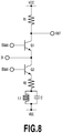
- FIG. 8 illustrates the configuration of the grounded base-type TIA according to the third embodiment of the present invention.
- a capacitive element C is connected in parallel to the inductor L1 at the grounded base-type TIA shown in FIG. 7 .
- the impedance Z seen from the emitter terminal of Q2 constituting the current source in the direction VEE can be calculated by the following formula.
- a current source can be realized that has a higher internal impedance.
- a resistance component parasitic in the inductor L1 for example prevents the impedance seen from the emitter terminal in the direction VEE from increasing to ⁇ .
- the impedance can be made to be seemingly high in the vicinity of the resonance point.
- the third embodiment is effectively applied to a case where the amplifier cannot include therein an inductor having a sufficiently-high inductance.
- an LC resonance point designed in the frequency band of the TIA can provide a particularly-high internal impedance.
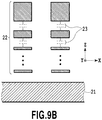
- FIGs. 9A and 9B illustrate a resonance circuit formed in the TIA chip.
- FIG. 9A is a bird's - eye view illustrating the inductor element having a three-dimensional structure formed in the TIA chip.
- a substrate 21 has thereon a plurality of wiring layers having partially-cut spiral wirings. The wirings among the respective wiring layers are cascade-connected so as to provide one continuous wiring, thereby forming an inductor element 22. The respective wiring layers are not shown.
- an LC parallel circuit using a parasitic capacitance 23 between wirings can be configured as shown in FIG. 9B .
- this configuration can have a high inductance value and also can function as an LC resonance circuit, thus providing a further-higher noise reduction effect.
- FIG. 10 illustrates the grounded base-type TIA according to the fourth embodiment of the present invention.
- This configuration is obtained by adding the transistor Q3 in the grounded base-type TIA shown in FIG. 6 to provide a cascade-type structure, and includes the second current source consisting of the transistor Q4 and the inductor L2 between the positive-side power source voltage VCC and the collector terminal of the transistor Q1.
- the second current source consisting of the transistor Q4 and the inductor L2
- the current flowing in the transistor Q1 of the amplification stage can be increased, achieving an operation in a wide band than in the case of the conventional TIA shown in FIG. 2 .
- the cascade structure provided by the transistor Q3 can provide an effect to prevent the deterioration of the frequency band caused by the parasitic capacitance involved in the second current source.
- FIG. 11 illustrates the result of simulating the transimpedance gain Zt and the input noise-converted current density Ieq characteristic of the grounded base-type TIA.
- the reference numeral A represents the grounded base-type TIA (having the inductors L1 and L2) of the fourth embodiment shown in FIG. 10 .
- the reference numeral B represents the grounded base-type TIA (having only the inductor L1) of the first embodiment shown in FIG. 6 .
- the reference numeral C represents the grounded base-type TIA as a modification of the fourth embodiment in which no inductor L1 is provided and only the inductor L2 is provided.
- the reference numeral D represents the conventional grounded base-type TIA shown in FIG. 2 (in which no inductor L1 or L2 is provided).
- the insertion of the inductors L1 and L2 can improve the input noise-converted current density Ieq without causing a change of the transimpedance gain Zt.
- the invention is not limited to the current source inserted between the input terminal IN and the negative-side power source voltage VEE and also can be applied to a current source configured by the transistor Q4 and the inductor L2 in the cascade-type TIA.
- this embodiment is not limited to the TIA including the current source that is inserted between the input terminal IN and the negative-side power source voltage VEE.
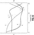
- FIG. 12 illustrates the simulation result.
- the reference numeral A illustrates the grounded base-type TIA (having the resistance R, the inductor L1, and the capacitive element C) of the third embodiment shown in FIG. 8 .
- the reference numeral B represents the grounded base-type TIA (having only the resistance R and the inductor L1) of the second embodiment shown in FIG. 7 .
- the reference numeral C represents the conventional grounded base-type TIA (in which no inductor L1 or L2 is provided) of FIG. 2 .
- the insertion of the capacitive element C can improve, without causing a change of the transimpedance gain Zt, the input noise-converted current density Ieq, thus minimizing, in the frequency band of the TIA, the noise caused by the current source.
- FIG. 13 illustrates the configuration of the grounded emitter-type TIA according to the fifth embodiment of the present invention.
- the grounded emitter-type TIA includes: the transistor Q3 and the inductor L1 serially inserted between the input terminal IN and the negative-side power source voltage VEE; the amplification stage consisting of the transistor Q1 and the resistances R1 and R2; an output stage (emitter follower) consisting of the transistor Q2 and the resistance R3; and the feedback resister R4 inserted between the output terminal OUT and the input terminal IN.
- the transistor Q3 has a base terminal connected to the current control bias to control the DC current flowing in the transistor Q1 and the DC component of the input signal current.
- the emitter terminal of the transistor Q3 connected to the inductor element constitutes a current source having a high internal impedance to thereby suppress the deterioration of the noise characteristic of the TIA due to the current source.
- the amplification stage has the transistor Q1 that has the base terminal connected to the input terminal IN, that has the emitter terminal connected to the negative-side power source voltage VEE via the resistance R2, and that has the collector terminal is connected to the base terminal of the transistor Q2 of the output stage.
- the output stage has the transistor Q2 that has the collector terminal connected to the positive-side power source voltage VCC and that has the emitter terminal connected to the negative-side power source voltage VEE via the resistance R3.
- the transistor Q1 has the collector terminal connected to the emitter follower of the output stage and thus can be considered as equivalent to the one being connected to the output terminal OUT.
- FIG. 14 illustrates the result of simulating the transimpedance gain Zt and the input noise-converted current density Ieq characteristic of the grounded emitter-type TIA.
- the reference numeral A represents the grounded emitter-type TIA (having the inductor L1) of the fifth embodiment shown in FIG. 13 .
- the reference numeral B represents the conventional grounded emitter-type TIA (having no inductor L1) shown in FIG. 1 .
- the insertion of the inductor L1 can improve the input noise-converted current density Ieq without causing a change of the transimpedance gain Zt.
- This embodiment also may be applied to the configuration as in the grounded base-type TIA in which resistance is inserted to have a serial connection to the inductor element.
- the bipolar transistor a part or all of the transistors also may be substituted with FET elements.
- the TIA including a current source is not limited to the current source inserted between the input terminal IN and the negative-side power source voltage VEE.
- FIG. 15 illustrates the configuration of the RGC-type TIA according to the sixth embodiment of the present invention.
- the amplification stage consisting of the transistor Q1 and the resistance R1 is cascade-connected to the transistor Q2 and resistance R2.
- the transistor Q2 and the inductor L1 are inserted between the input terminal IN and the negative-side power source voltage VEE.
- the transistor Q2 has a base terminal connected to the current control bias to control the DC current flowing in the transistor Q1 and the DC component of the input signal current.
- the emitter terminal of the transistor Q2 connected to the inductor element constitutes a current source having an internal impedance, thereby suppressing the deterioration of the noise characteristic of the TIA due to the current source.
- This embodiment also may be applied to a configuration as in the grounded base-type TIA in which resistance is inserted in a serial manner to the inductor element.
- a part or all of the transistors also may be substituted with FET elements.
- the TIA including a current source is not limited to the current source inserted between the input terminal IN and the negative-side power source voltage VEE.
- an amplifier applied to the TIA in which a transistor function as a current source has an emitter terminal connected to an inductor element.
- This configuration realize a current source having a high internal impedance. This can consequently minimize the noise caused by the current source, thus realizing a low-noise TIA.
Applications Claiming Priority (2)
| Application Number | Priority Date | Filing Date | Title |
|---|---|---|---|
| JP2015133047A JP6397374B2 (ja) | 2015-07-01 | 2015-07-01 | 増幅器 |
| PCT/JP2016/003166 WO2017002374A1 (ja) | 2015-07-01 | 2016-07-01 | 増幅器 |
Publications (2)
| Publication Number | Publication Date |
|---|---|
| EP3319231A1 true EP3319231A1 (de) | 2018-05-09 |
| EP3319231A4 EP3319231A4 (de) | 2018-12-05 |
Family
ID=57608496
Family Applications (1)
| Application Number | Title | Priority Date | Filing Date |
|---|---|---|---|
| EP16817484.5A Withdrawn EP3319231A4 (de) | 2015-07-01 | 2016-07-01 | Verstärker |
Country Status (5)
| Country | Link |
|---|---|
| US (1) | US10892716B2 (de) |
| EP (1) | EP3319231A4 (de) |
| JP (1) | JP6397374B2 (de) |
| CN (1) | CN107683566B (de) |
| WO (1) | WO2017002374A1 (de) |
Families Citing this family (1)
| Publication number | Priority date | Publication date | Assignee | Title |
|---|---|---|---|---|
| JP2020077956A (ja) * | 2018-11-07 | 2020-05-21 | 住友電気工業株式会社 | 光受信回路 |
Family Cites Families (15)
| Publication number | Priority date | Publication date | Assignee | Title |
|---|---|---|---|---|
| US3331028A (en) * | 1965-01-21 | 1967-07-11 | Avco Corp | Multistage transistor amplifier in which the impedances of the various stages are successively varied to control gain |
| CA2021380C (en) * | 1989-07-21 | 1994-05-10 | Takuji Yamamoto | Equalizing and amplifying circuit in an optical signal receiving apparatus |
| DE4104980C3 (de) * | 1991-02-19 | 1996-02-08 | Telefunken Microelectron | Verstärkerstufe für niederohmige Wechselspannungs-Quellen |
| JPH09260973A (ja) * | 1996-03-26 | 1997-10-03 | Toyota Central Res & Dev Lab Inc | 差動増幅器 |
| US5945878A (en) * | 1998-02-17 | 1999-08-31 | Motorola, Inc. | Single-ended to differential converter |
| US6331921B1 (en) * | 1998-07-06 | 2001-12-18 | Agilent Technologies, Inc | Magneto-resistive head read amplifier |
| JP3522630B2 (ja) * | 2000-03-08 | 2004-04-26 | 日本電信電話株式会社 | 単相信号/差動信号変換型の電圧増幅器 |
| JP2004207874A (ja) * | 2002-12-24 | 2004-07-22 | Toshiba Corp | 周波数変換器及び無線通信端末装置 |
| US7505696B2 (en) | 2004-08-12 | 2009-03-17 | Triaccess Technologies, Inc. | Optical receiver with increased dynamic range |
| TWI340537B (en) * | 2006-02-14 | 2011-04-11 | Richwave Technology Corp | Single-ended input to differential-ended output low noise amplifier implemented with cascode and cascade topology |
| JP2009290520A (ja) * | 2008-05-29 | 2009-12-10 | Hitachi Ltd | トランスインピーダンスアンプ、レギュレイテッド型トランスインピーダンスアンプ及び光受信器 |
| US8787030B2 (en) | 2008-10-30 | 2014-07-22 | Sumitomo Electric Industries, Ltd. | Multilayer circuit board with resin bases and separators |
| EP2736168B1 (de) | 2010-03-09 | 2015-05-06 | Marvell World Trade Ltd. | Verstärker der Klasse AB |
| US8487702B2 (en) * | 2011-09-21 | 2013-07-16 | Realtek Semiconductor Corp. | Transimpedance amplifier and method thereof |
| EP2869465B1 (de) * | 2013-11-01 | 2016-05-25 | Nxp B.V. | HF-Verstärker |
-
2015
- 2015-07-01 JP JP2015133047A patent/JP6397374B2/ja active Active
-
2016
- 2016-07-01 WO PCT/JP2016/003166 patent/WO2017002374A1/ja active Application Filing
- 2016-07-01 US US15/735,553 patent/US10892716B2/en active Active
- 2016-07-01 EP EP16817484.5A patent/EP3319231A4/de not_active Withdrawn
- 2016-07-01 CN CN201680035555.7A patent/CN107683566B/zh active Active
Also Published As
| Publication number | Publication date |
|---|---|
| JP2017017558A (ja) | 2017-01-19 |
| WO2017002374A1 (ja) | 2017-01-05 |
| US10892716B2 (en) | 2021-01-12 |
| CN107683566A (zh) | 2018-02-09 |
| JP6397374B2 (ja) | 2018-09-26 |
| CN107683566B (zh) | 2021-08-20 |
| EP3319231A4 (de) | 2018-12-05 |
| US20200036344A1 (en) | 2020-01-30 |
Similar Documents
| Publication | Publication Date | Title |
|---|---|---|
| US7521996B2 (en) | Differential amplifier and radio system with a differential amplifier | |
| US6765377B1 (en) | Q-emphasized amplifier with inductor-based bandwidth booster | |
| JP2001160723A (ja) | 分布増幅器 | |
| US10797802B2 (en) | Optical receiver | |
| CN108429545B (zh) | 可调阻值式虚拟电阻 | |
| US10892716B2 (en) | Amplifier | |
| KR20210134217A (ko) | 세미-캐스코딩을 갖는 전류 미러 배열들 | |
| US7508264B1 (en) | DC-couples RF multi-stage amplifier | |
| JP6515493B2 (ja) | 増幅回路の帯域幅を改善するための方法及び回路 | |
| US7868688B2 (en) | Leakage independent very low bandwith current filter | |
| US7443207B2 (en) | Differential output circuit with stable duty | |
| US20100182093A1 (en) | Single-ended to differential converting apparatus and rf receiving apparatus | |
| US10666212B2 (en) | Driver circuit and optical transmitter | |
| EP3826176B1 (de) | Eingangspuffer mit hoher linearität | |
| US10911007B2 (en) | High-frequency amplifier circuitry and semiconductor device | |
| US20100127772A1 (en) | Feedback amplifier and audio system thererof | |
| US8203384B1 (en) | Amplifier | |
| US20050057309A1 (en) | Transistor amplifier | |
| US7196573B1 (en) | Systems and methods for creating complex poles | |
| US7612609B1 (en) | Self-stabilizing differential load circuit with well controlled complex impedance | |
| US9716499B2 (en) | Current amplifier and transmitter using the same | |
| US9312819B1 (en) | Active inductor and associated amplifying circuit | |
| US20210344095A1 (en) | Directional coupler and semiconductor chip | |
| JP4823500B2 (ja) | 多段高周波増幅器 | |
| US8085096B2 (en) | Apparatus and method for improved amplifier shunt-peak loading |
Legal Events
| Date | Code | Title | Description |
|---|---|---|---|
| PUAI | Public reference made under article 153(3) epc to a published international application that has entered the european phase |
Free format text: ORIGINAL CODE: 0009012 |
|
| 17P | Request for examination filed |
Effective date: 20171215 |
|
| AK | Designated contracting states |
Kind code of ref document: A1 Designated state(s): AL AT BE BG CH CY CZ DE DK EE ES FI FR GB GR HR HU IE IS IT LI LT LU LV MC MK MT NL NO PL PT RO RS SE SI SK SM TR |
|
| AX | Request for extension of the european patent |
Extension state: BA ME |
|
| DAV | Request for validation of the european patent (deleted) | ||
| DAX | Request for extension of the european patent (deleted) | ||
| A4 | Supplementary search report drawn up and despatched |
Effective date: 20181030 |
|
| RIC1 | Information provided on ipc code assigned before grant |
Ipc: H03F 3/08 20060101ALI20181024BHEP Ipc: H03F 1/22 20060101ALI20181024BHEP Ipc: H04B 10/66 20130101ALI20181024BHEP Ipc: H03F 3/04 20060101ALI20181024BHEP Ipc: H03F 1/26 20060101AFI20181024BHEP |
|
| 17Q | First examination report despatched |
Effective date: 20190605 |
|
| STAA | Information on the status of an ep patent application or granted ep patent |
Free format text: STATUS: THE APPLICATION HAS BEEN WITHDRAWN |
|
| 18W | Application withdrawn |
Effective date: 20190823 |