EP3310941B1 - Vorrichtung und verfahren zur beschichtung von linsen - Google Patents
Vorrichtung und verfahren zur beschichtung von linsen Download PDFInfo
- Publication number
- EP3310941B1 EP3310941B1 EP16730695.0A EP16730695A EP3310941B1 EP 3310941 B1 EP3310941 B1 EP 3310941B1 EP 16730695 A EP16730695 A EP 16730695A EP 3310941 B1 EP3310941 B1 EP 3310941B1
- Authority
- EP
- European Patent Office
- Prior art keywords
- target
- lenses
- lens
- carrier
- coating
- Prior art date
- Legal status (The legal status is an assumption and is not a legal conclusion. Google has not performed a legal analysis and makes no representation as to the accuracy of the status listed.)
- Active
Links
- 238000000576 coating method Methods 0.000 title claims description 71
- 239000011248 coating agent Substances 0.000 title claims description 67
- 238000000034 method Methods 0.000 title claims description 14
- 238000004544 sputter deposition Methods 0.000 claims description 25
- 230000007423 decrease Effects 0.000 claims description 3
- 230000005484 gravity Effects 0.000 claims description 2
- 238000003780 insertion Methods 0.000 claims 1
- 230000037431 insertion Effects 0.000 claims 1
- 239000007789 gas Substances 0.000 description 10
- 239000000758 substrate Substances 0.000 description 4
- 239000013077 target material Substances 0.000 description 4
- 238000001755 magnetron sputter deposition Methods 0.000 description 3
- 230000003287 optical effect Effects 0.000 description 3
- 230000008569 process Effects 0.000 description 3
- XKRFYHLGVUSROY-UHFFFAOYSA-N Argon Chemical compound [Ar] XKRFYHLGVUSROY-UHFFFAOYSA-N 0.000 description 2
- IJGRMHOSHXDMSA-UHFFFAOYSA-N Atomic nitrogen Chemical compound N#N IJGRMHOSHXDMSA-UHFFFAOYSA-N 0.000 description 2
- 238000010276 construction Methods 0.000 description 2
- 238000011109 contamination Methods 0.000 description 2
- 238000010586 diagram Methods 0.000 description 2
- 239000000463 material Substances 0.000 description 2
- 230000007704 transition Effects 0.000 description 2
- 241000310247 Amyna axis Species 0.000 description 1
- UFHFLCQGNIYNRP-UHFFFAOYSA-N Hydrogen Chemical compound [H][H] UFHFLCQGNIYNRP-UHFFFAOYSA-N 0.000 description 1
- 230000003667 anti-reflective effect Effects 0.000 description 1
- 229910052786 argon Inorganic materials 0.000 description 1
- QVGXLLKOCUKJST-UHFFFAOYSA-N atomic oxygen Chemical compound [O] QVGXLLKOCUKJST-UHFFFAOYSA-N 0.000 description 1
- 230000008859 change Effects 0.000 description 1
- 238000004140 cleaning Methods 0.000 description 1
- 230000008878 coupling Effects 0.000 description 1
- 238000010168 coupling process Methods 0.000 description 1
- 238000005859 coupling reaction Methods 0.000 description 1
- 238000005520 cutting process Methods 0.000 description 1
- 230000003247 decreasing effect Effects 0.000 description 1
- 238000000151 deposition Methods 0.000 description 1
- 230000008021 deposition Effects 0.000 description 1
- 238000011161 development Methods 0.000 description 1
- 230000018109 developmental process Effects 0.000 description 1
- 238000009826 distribution Methods 0.000 description 1
- 230000005684 electric field Effects 0.000 description 1
- 239000001257 hydrogen Substances 0.000 description 1
- 229910052739 hydrogen Inorganic materials 0.000 description 1
- 150000002500 ions Chemical class 0.000 description 1
- 238000012423 maintenance Methods 0.000 description 1
- 229910052757 nitrogen Inorganic materials 0.000 description 1
- 229910052756 noble gas Inorganic materials 0.000 description 1
- 239000001301 oxygen Substances 0.000 description 1
- 229910052760 oxygen Inorganic materials 0.000 description 1
- 239000007787 solid Substances 0.000 description 1
- 229910052717 sulfur Inorganic materials 0.000 description 1
Images


Classifications
-
- B—PERFORMING OPERATIONS; TRANSPORTING
- B29—WORKING OF PLASTICS; WORKING OF SUBSTANCES IN A PLASTIC STATE IN GENERAL
- B29D—PRODUCING PARTICULAR ARTICLES FROM PLASTICS OR FROM SUBSTANCES IN A PLASTIC STATE
- B29D11/00—Producing optical elements, e.g. lenses or prisms
- B29D11/00865—Applying coatings; tinting; colouring
-
- C—CHEMISTRY; METALLURGY
- C23—COATING METALLIC MATERIAL; COATING MATERIAL WITH METALLIC MATERIAL; CHEMICAL SURFACE TREATMENT; DIFFUSION TREATMENT OF METALLIC MATERIAL; COATING BY VACUUM EVAPORATION, BY SPUTTERING, BY ION IMPLANTATION OR BY CHEMICAL VAPOUR DEPOSITION, IN GENERAL; INHIBITING CORROSION OF METALLIC MATERIAL OR INCRUSTATION IN GENERAL
- C23C—COATING METALLIC MATERIAL; COATING MATERIAL WITH METALLIC MATERIAL; SURFACE TREATMENT OF METALLIC MATERIAL BY DIFFUSION INTO THE SURFACE, BY CHEMICAL CONVERSION OR SUBSTITUTION; COATING BY VACUUM EVAPORATION, BY SPUTTERING, BY ION IMPLANTATION OR BY CHEMICAL VAPOUR DEPOSITION, IN GENERAL
- C23C14/00—Coating by vacuum evaporation, by sputtering or by ion implantation of the coating forming material
- C23C14/22—Coating by vacuum evaporation, by sputtering or by ion implantation of the coating forming material characterised by the process of coating
- C23C14/34—Sputtering
- C23C14/3407—Cathode assembly for sputtering apparatus, e.g. Target
-
- C—CHEMISTRY; METALLURGY
- C23—COATING METALLIC MATERIAL; COATING MATERIAL WITH METALLIC MATERIAL; CHEMICAL SURFACE TREATMENT; DIFFUSION TREATMENT OF METALLIC MATERIAL; COATING BY VACUUM EVAPORATION, BY SPUTTERING, BY ION IMPLANTATION OR BY CHEMICAL VAPOUR DEPOSITION, IN GENERAL; INHIBITING CORROSION OF METALLIC MATERIAL OR INCRUSTATION IN GENERAL
- C23C—COATING METALLIC MATERIAL; COATING MATERIAL WITH METALLIC MATERIAL; SURFACE TREATMENT OF METALLIC MATERIAL BY DIFFUSION INTO THE SURFACE, BY CHEMICAL CONVERSION OR SUBSTITUTION; COATING BY VACUUM EVAPORATION, BY SPUTTERING, BY ION IMPLANTATION OR BY CHEMICAL VAPOUR DEPOSITION, IN GENERAL
- C23C14/00—Coating by vacuum evaporation, by sputtering or by ion implantation of the coating forming material
- C23C14/22—Coating by vacuum evaporation, by sputtering or by ion implantation of the coating forming material characterised by the process of coating
- C23C14/34—Sputtering
- C23C14/35—Sputtering by application of a magnetic field, e.g. magnetron sputtering
- C23C14/352—Sputtering by application of a magnetic field, e.g. magnetron sputtering using more than one target
-
- C—CHEMISTRY; METALLURGY
- C23—COATING METALLIC MATERIAL; COATING MATERIAL WITH METALLIC MATERIAL; CHEMICAL SURFACE TREATMENT; DIFFUSION TREATMENT OF METALLIC MATERIAL; COATING BY VACUUM EVAPORATION, BY SPUTTERING, BY ION IMPLANTATION OR BY CHEMICAL VAPOUR DEPOSITION, IN GENERAL; INHIBITING CORROSION OF METALLIC MATERIAL OR INCRUSTATION IN GENERAL
- C23C—COATING METALLIC MATERIAL; COATING MATERIAL WITH METALLIC MATERIAL; SURFACE TREATMENT OF METALLIC MATERIAL BY DIFFUSION INTO THE SURFACE, BY CHEMICAL CONVERSION OR SUBSTITUTION; COATING BY VACUUM EVAPORATION, BY SPUTTERING, BY ION IMPLANTATION OR BY CHEMICAL VAPOUR DEPOSITION, IN GENERAL
- C23C14/00—Coating by vacuum evaporation, by sputtering or by ion implantation of the coating forming material
- C23C14/22—Coating by vacuum evaporation, by sputtering or by ion implantation of the coating forming material characterised by the process of coating
- C23C14/50—Substrate holders
- C23C14/505—Substrate holders for rotation of the substrates
-
- G—PHYSICS
- G02—OPTICS
- G02B—OPTICAL ELEMENTS, SYSTEMS OR APPARATUS
- G02B1/00—Optical elements characterised by the material of which they are made; Optical coatings for optical elements
- G02B1/10—Optical coatings produced by application to, or surface treatment of, optical elements
-
- H—ELECTRICITY
- H01—ELECTRIC ELEMENTS
- H01J—ELECTRIC DISCHARGE TUBES OR DISCHARGE LAMPS
- H01J37/00—Discharge tubes with provision for introducing objects or material to be exposed to the discharge, e.g. for the purpose of examination or processing thereof
- H01J37/32—Gas-filled discharge tubes
- H01J37/32009—Arrangements for generation of plasma specially adapted for examination or treatment of objects, e.g. plasma sources
- H01J37/32403—Treating multiple sides of workpieces, e.g. 3D workpieces
-
- H—ELECTRICITY
- H01—ELECTRIC ELEMENTS
- H01J—ELECTRIC DISCHARGE TUBES OR DISCHARGE LAMPS
- H01J37/00—Discharge tubes with provision for introducing objects or material to be exposed to the discharge, e.g. for the purpose of examination or processing thereof
- H01J37/32—Gas-filled discharge tubes
- H01J37/32431—Constructional details of the reactor
- H01J37/32715—Workpiece holder
-
- H—ELECTRICITY
- H01—ELECTRIC ELEMENTS
- H01J—ELECTRIC DISCHARGE TUBES OR DISCHARGE LAMPS
- H01J37/00—Discharge tubes with provision for introducing objects or material to be exposed to the discharge, e.g. for the purpose of examination or processing thereof
- H01J37/32—Gas-filled discharge tubes
- H01J37/32431—Constructional details of the reactor
- H01J37/32733—Means for moving the material to be treated
- H01J37/32752—Means for moving the material to be treated for moving the material across the discharge
-
- H—ELECTRICITY
- H01—ELECTRIC ELEMENTS
- H01J—ELECTRIC DISCHARGE TUBES OR DISCHARGE LAMPS
- H01J37/00—Discharge tubes with provision for introducing objects or material to be exposed to the discharge, e.g. for the purpose of examination or processing thereof
- H01J37/32—Gas-filled discharge tubes
- H01J37/34—Gas-filled discharge tubes operating with cathodic sputtering
- H01J37/3402—Gas-filled discharge tubes operating with cathodic sputtering using supplementary magnetic fields
- H01J37/3405—Magnetron sputtering
-
- H—ELECTRICITY
- H01—ELECTRIC ELEMENTS
- H01J—ELECTRIC DISCHARGE TUBES OR DISCHARGE LAMPS
- H01J37/00—Discharge tubes with provision for introducing objects or material to be exposed to the discharge, e.g. for the purpose of examination or processing thereof
- H01J37/32—Gas-filled discharge tubes
- H01J37/34—Gas-filled discharge tubes operating with cathodic sputtering
- H01J37/3411—Constructional aspects of the reactor
- H01J37/3414—Targets
- H01J37/3417—Arrangements
-
- H—ELECTRICITY
- H01—ELECTRIC ELEMENTS
- H01J—ELECTRIC DISCHARGE TUBES OR DISCHARGE LAMPS
- H01J37/00—Discharge tubes with provision for introducing objects or material to be exposed to the discharge, e.g. for the purpose of examination or processing thereof
- H01J37/32—Gas-filled discharge tubes
- H01J37/34—Gas-filled discharge tubes operating with cathodic sputtering
- H01J37/3411—Constructional aspects of the reactor
- H01J37/3414—Targets
- H01J37/342—Hollow targets
-
- H—ELECTRICITY
- H01—ELECTRIC ELEMENTS
- H01J—ELECTRIC DISCHARGE TUBES OR DISCHARGE LAMPS
- H01J37/00—Discharge tubes with provision for introducing objects or material to be exposed to the discharge, e.g. for the purpose of examination or processing thereof
- H01J37/32—Gas-filled discharge tubes
- H01J37/34—Gas-filled discharge tubes operating with cathodic sputtering
- H01J37/3411—Constructional aspects of the reactor
- H01J37/3414—Targets
- H01J37/3423—Shape
-
- H—ELECTRICITY
- H01—ELECTRIC ELEMENTS
- H01J—ELECTRIC DISCHARGE TUBES OR DISCHARGE LAMPS
- H01J37/00—Discharge tubes with provision for introducing objects or material to be exposed to the discharge, e.g. for the purpose of examination or processing thereof
- H01J37/32—Gas-filled discharge tubes
- H01J37/34—Gas-filled discharge tubes operating with cathodic sputtering
- H01J37/3464—Operating strategies
- H01J37/347—Thickness uniformity of coated layers or desired profile of target erosion
Definitions
- the present invention relates to a device for coating lenses according to the preamble of claim 1 and a method for coating lenses according to the preamble of claim 14.
- the present invention relates generally to the coating of lenses by sputtering, which is also called cathode sputtering.
- sputtering which is also called cathode sputtering.
- atoms are released from a solid body, the so-called target, by the impact of high-energy ions and change into a gas phase.
- the present invention relates to so-called magnetron sputtering, in which, in addition to an applied electric field, a magnetic field is also arranged behind the cathode or the target.
- the DE 40 10 495 C2 discloses an apparatus for coating a substrate with materials by sputtering, the substrate being rotatable about a stationary axis and the substrate being assigned two targets which are held inclined to the substrate surface. A uniform coating cannot be achieved here, or at most only with great difficulty.
- the DE 295 05 497 U1 discloses a coating station for coating lenses by sputtering, the lenses being moved in a planetary arrangement over a planar sputtering source.
- the construction effort is considerable here and the charging of the coating station with lenses to be coated is complex. Furthermore, an optimal, uniform coating cannot be achieved, or only with great difficulty.
- the WO 03/023813 A1 discloses a device for coating lenses by means of pulse magnetron sputtering, the lenses being moved linearly along the longitudinal extension of two tubular, parallel targets and thereby also rotating. A uniform coating of the lenses cannot be achieved here, or at most only with great difficulty.
- the JP 2001 355068 A discloses a sputtering device and a coating method.
- the device has a single, flat target.
- the lens is arranged centrally over the target, so that it extends at least substantially over the entire target length.
- a homogeneous coating of the lens is achieved by adapting the voltage profile across the target to the lens shape, so that different sputtering rates result in different target areas.
- the present invention is based on the object of specifying a device and a method for coating lenses, with a very uniform coating, in particular of curved surfaces of the lenses, being made possible with a simple structure and / or with simple loading.
- the device has an elongate or tubular target and the lens to be coated can be rotated about an axis which is stationary relative to the target.
- the lens cannot be moved linearly, but is preferably a stationary arrangement, the target and the lens preferably rotating about stationary axes. In this way, a particularly uniform coating of the lens can be achieved with little structural effort.
- the lens to be coated is held above the target both in a first, at least substantially homogeneous area and in a second, inhomogeneous area of a rate profile of the removal of a target and is rotated in the process. This enables a particularly uniform coating, in particular of a curved surface of the lens.
- the lens to be coated is held in an end region or its vicinity above the preferably elongated or tubular target. In this way, particularly good utilization of the release rate, which is increased towards the end of the target, and thus improved utilization of the atomized target material can take place.
- two elongate or tubular, in particular parallel targets are preferably used for coating curved ones
- the lenses are arranged in pairs over the targets and preferably each rotate about a stationary axis. This enables a simple, compact design, with very uniform coatings on the lenses being achievable.
- the device preferably has a carrier which can be exchanged together with at least two lenses. This enables a very simple and quick loading of the device.
- a target with an outer diameter that varies over its axial extent or longitudinal extent is preferably used for coating a lens.
- the rate profile can be influenced, in particular evened out, and / or in particular a very uniform or more uniform coating on the lens or another coating process on the lens can be achieved or facilitated.
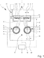
- Fig. 1 shows in a very schematic section a device 1 according to the proposal for coating lenses 2, preferably optical or ophthalmic lenses or spectacle lenses, in particular made of plastic.
- the device 1 is designed in particular for coating the lenses 2 by sputtering, also called cathode sputtering. So-called magnetron sputtering is particularly preferred. In addition to an electrically applied field, a magnetic field is also used or applied, which will be discussed in more detail later.
- Curved, in particular concave surfaces of the lenses 2 are particularly preferably coated according to the invention.
- a curved surface is indicated schematically in the lens 2 shown on the right-hand side.
- convex surfaces or other surfaces of the lenses 2 can also be coated accordingly.
- the device 1 has at least one sputter source 3, here preferably two sputter sources 3.
- the device 1 or the respective sputtering source 3 has a target 4, the material of which is removed during coating or sputtering and - especially together with other components of the gas atmosphere - forms the desired coating on the respective lens 2 or its surface to be coated.
- Fig. 2 shows the device 1 or sputter sources 3 in a schematic plan view.
- the sputter sources 3 or targets 4 are preferably at least substantially elongated or tubular or cylindrical.
- the targets 4 are in particular hollow-cylindrical or tubular.
- the sputter sources 3 or targets 4 are preferably arranged parallel to one another.
- the targets 4 are preferably rotatable or rotatable about axes of rotation D.
- the axes of rotation D preferably run in a common plane and / or in particular parallel to one another, as in FIGS Fig. 1 and 2 indicated, but can alternatively also be inclined to one another.
- the axes of rotation D preferably correspond to the longitudinal axes of the sputtering sources 3.
- the sputter sources 3 or targets 4 are particularly preferably constructed identically and / or constructed so that primarily only the construction of a sputter source 3 or a target 4 will be discussed below. However, the sputter sources 3 or targets 4 can also be designed differently in principle.
- the sputter source 3 preferably has a magnet arrangement 5 which is assigned to the respective target 4 for generating the aforementioned magnetic field and thus a directed sputter cloud S, as in FIG Fig. 1 indicated schematically.
- the magnet arrangement 5 is arranged below or in the respective target 4.
- the device 1 has a voltage source 6, as in FIG Fig. 1 indicated in order to be able to operate the sputter sources 3 or targets 4 - in particular alternately - as cathodes or to be able to apply the required voltage, in particular in the form of pulses, for sputtering.
- the sputter sources 3 or targets 4 are particularly preferably operated or acted upon alternately with direct current (pulses). This is also known as "Bi-polar DC". A sputter source 3 or a target 4 then alternately serves as the cathode and the other sputter source 3 or the other target 4 as the anode.
- operation with alternating current or some other operation can take place.
- one or more additional or separate anodes can also be used, even if this is not preferred.
- the device 1 preferably has a coating chamber 7 in which the coating takes place or the sputter sources 3 are arranged.
- the preferred alternating operation of the sputter sources 3 or targets 4 as cathode and anode means that no housing-side or fixed counter-electrode is required.
- the coating chamber 7 is not used as a counter electrode. In this way, undesired contamination or deposition of target material on the counter electrode can be minimized or a particularly stable process or coating can be achieved even independently of contamination of the coating chamber 7. Correspondingly, the necessary cleaning and maintenance can be reduced.
- the targets 4 can be changed very easily. This also makes service easier.
- the coating chamber 7 can in particular be evacuated in the desired manner by means of a device 8, which is only indicated schematically here, such as a connection, a vacuum pump or the like.
- the device 1 or coating chamber 7 preferably has a schematically indicated gas supply 9, in particular in the form of a gas lance extending into the coating space.
- the device 1 preferably has a carrier 10 for holding the lenses 2, as in FIG Fig. 1 indicated.
- the lenses 2 to be coated are preferably each rotatable or rotatable about an axis A.
- the device 1 or the carrier 10 is designed for corresponding rotatable mounting and in particular for correspondingly driving the lenses 2.
- the device 1 has a corresponding, in Fig. 1 only schematically indicated rotary drive 11, preferably to drive all lenses 2 of the carrier 10 together.
- the carrier 10 is preferably exchangeable together with at least two lenses 2 or all lenses 2 or here four lenses 2 that are coated simultaneously in the device 1 or coating chamber 7.
- the carrier 10 holds the lenses 2 - in particular about their own or different axes A - rotatably, particularly preferably rotatably coupled.
- the carrier 10 has a rotary coupling 12, for example via a corresponding gear, as in FIG Fig. 1 indicated schematically.
- the carrier 10 itself is not moved during the coating, but rather only the lenses 2 held by it are rotated.
- the carrier 10 is when it is inserted or pushed into the device 1 or coating chamber 7 can be automatically coupled in terms of drive or gear, in particular to the rotary drive 11 or the like of the device 1.
- the carrier 10 allows the device 1 or coating chamber 7 to be quickly loaded with the lenses 2 to be coated or the coated lenses 2 to be removed quickly.
- the device 1 or coating chamber 7 can preferably be charged with the lenses 2 or the carrier 10 to be coated via an access opening (not shown).
- the access opening can preferably be closed in a gas-tight manner by means of the carrier 10 or by a closure (not shown).
- the coating chamber 7 can preferably be closed in a gas-tight manner for coating.
- the carrier 10 can preferably generally be used in devices for coating lenses 2, in particular also in coating processes other than sputtering.
- the axes of rotation D or longitudinal extensions L of the targets 4 preferably run in a common plane, particularly preferably a horizontal plane.
- the lenses 2 are preferably arranged above the aforementioned plane.
- Each lens 2 is preferably arranged above an associated target 4.
- the term “above” can refer to the vertical height with respect to the assigned target 4 and / or to the fact that the surface of the lens 2 to be coated has at least one surface normal that intersects the target 4 and particularly preferably its axis of rotation D.
- the lenses 2 are preferably assigned in pairs to a sputtering source 3 or a target 4.
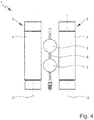
- two lenses 2 are arranged over a common target 4, as in FIG Fig. 2 and in the schematic side view according to Fig. 3 indicated.
- the device 1 or the carrier 10 is particularly preferably designed to accommodate two pairs of lenses 2, ie a total of four lenses 2, two lenses 2 being assigned to a common sputtering source 3 or a common target 4.
- the preferred arrangement and alignment of such a pair of lenses 2, which are assigned to a common target 4, will be discussed in greater detail below.
- the lenses 2 assigned to a common target 4 are preferably arranged offset in a direction parallel to the longitudinal extension L or axis of rotation D of the target 4. This direction is also called the X-direction or X-axis, especially in the case of the in Fig. 3 referred to schematically indicated diagram.
- the lenses 2 or their axes A are preferably arranged symmetrically with respect to the longitudinal extension L of the target 4 and / or have an offset or distance E from the respective end of the target 4 in the axial direction or X direction.
- the lenses 2 are arranged in an end region or its vicinity of the respective target 4, as in FIG Fig. 1 and 2 indicated.
- FIG. 3 illustrates qualitatively the rate R of the removal of the target 4 during the coating as a function of the axial position or X position. This results in a rate profile P of the rate R over X, that is to say in the direction of the longitudinal extent L of the target 4.
- the rate profile P has a first, at least substantially homogeneous region B1 in the central axial region of the target 4.
- the rate R is therefore at least essentially constant in the first area B1 or varies only very slightly along the axial extent of the target 4 in this area B1, in particular less than 5%.
- “essentially constant” is preferably to be understood as meaning that the rate R along the longitudinal extent L - here in the region B1 - varies by less than 5%.
- the rate profile P also has a second, non-homogeneous or inhomogeneous area B2.
- the rate R varies very strongly, in particular increases sharply towards the end of the target 4, particularly preferably by more than 10%.
- the rate R of the removal of the target 4 in the second area B2, which increases towards the end of the target 4 or respective magnet arrangement 5, can be explained by the increased magnetic field strength in the end area.
- the lenses 2 are preferably each arranged in such a way - here in the axial extent L or X-direction over the target 4 - that the lens 2 is arranged or covers them both in the first area B1 and in the second area B2.
- the center or axis A of the respective lens 2 is particularly preferably arranged in the vicinity of the transition from the first area B1 to the second area B2.
- the deviation of the axis A from this transition is preferably less than 30%, in particular less than 20%, particularly preferably less than 10% of the lens diameter.
- the axis A, about which the lens 2 rotates during the coating, is preferably stationary or fixed relative to the target 4 or the sputtering source 3 or the axis of rotation D.
- the offset or distance E of the axis of rotation A of the lens 2 from the respective end of the target 4 is preferably more than 1.0 times or 1.5 times the lens diameter and / or target diameter.
- the distance E is preferably fixed.
- the distance E of the axis of rotation A of the lens 2 from the respective end of the target 4 is adapted or adjusted depending on the diameter and / or the curvature or shape of the lens 2 or surface to be coated.
- the (vertical) distance Z of the lens 2 from the assigned target 4 is in Fig. 1 indicated and is preferably more than 1.0 times the lens diameter or target diameter.
- the (vertical) distance Z of the lens 2 from the assigned target 4 is preferably more than approximately 60 mm and / or less than 150 mm, in particular less than 130 mm.
- the distance Z is preferably fixed.
- the (vertical) distance Z of the lens 2 from the assigned target 4 is adapted or adjusted as a function of the diameter and / or the curvature or shape of the lens 2 or surface to be coated.
- the target diameter is preferably about 70 to 130 mm.
- the target (outer) diameter is preferably at least substantially constant over the length.
- the target 4 is thus preferably designed to be cylindrical or hollow-cylindrical.
- the axes A of two lenses 2 assigned to a common target 4 preferably run in a common plane and in particular parallel to one another.
- the axes A preferably run transversely or perpendicularly to the target plane or the common plane of the axes of rotation D or to the axis of rotation D of the assigned target 4.
- the axes A can also be inclined relative to one another in their common plane, in particular towards one another or outwards or away from one another. Accordingly If the lenses 2 are then closer to one another or moved away from one another, in particular possibly so that the surfaces to be coated of the two lenses 2 are tilted somewhat towards one another or point somewhat more towards the center of the respective target 4. Accordingly, the inclination angle N of the axes A to the rotation axes D can vary from the preferred 90 degrees as shown in FIG Fig. 3 shown, differ and either less than 90 °, for example about 70 ° to 85 °, or more than 90 °, for example about 95 ° to 110 °.
- the angle of inclination N is preferably fixed. Particularly preferably, however, the angle of inclination N is optionally adapted or adjusted as a function of the diameter and / or the curvature or shape of the lens 2 or surface to be coated.
- the axis of rotation A of the lens 2 can also be shifted in the Y direction, i.e. in a direction transverse to the axis of rotation D in the horizontal direction or to the center between the two axes of rotation D of the targets 4, in particular so that an offset or distance V between the lens axis A and the associated target axis D forms, as in Fig. 1 indicated for the lens 2 arranged on the right side (the same applies, of course, preferably also to the lens 2 arranged on the left side).
- the offset or distance V is preferably less than 20%, in particular less than 10% of the lens diameter and / or target diameter.
- the distance V is preferably fixed.
- the distance V between the lens axis A and the assigned target axis D is adapted or adjusted as a function of the diameter and / or the curvature or shape of the lens 2 or surface to be coated.
- the angle of inclination N and / or the position of the axes A or the distances E, V and / or Z are preferably determined by the carrier 10.
- the gas supply 9 is preferably arranged below the sputtering sources 3 or targets 4 and / or between them, particularly preferably in the central plane M of the device 1 or coating chamber 7.
- the gas supply 9 is preferably tubular and / or rod-like and / or provided with gas outlets preferably arranged in a row and / or pointing upwards.
- the sputtering cloud S occurring during the coating is in each case at least substantially directed in a desired direction by means of the aforementioned magnetic field or the magnet arrangement 5.
- This in Fig. 1 The main direction H, indicated by dashed lines, of the spread of the sputter cloud S can be influenced, in particular fixed, by a corresponding arrangement or alignment of the magnet arrangement 5.
- the main direction H in the cutting plane is perpendicular to the axes of rotation D and / or the two targets 4, preferably inclined to one another and / or by the angle W (based on a parallel alignment).
- the angle W is preferably adjustable or adaptable, in particular by appropriate adjustment or control of the magnet arrangements 5.
- the angle W is preferably less than 10 °, in particular less than 7 °, particularly preferably less than 5 °.
- the main directions H of the two sputter clouds S can also run parallel to one another and / or perpendicular to the plane of extent of the targets 4 or plane with the axis of rotation D.
- the main directions H preferably run vertically upwards or contain such a directional component. Alternatively, the main directions H are aligned horizontally. The arrangement of the lenses 2 and sputter sources 3 or targets 4 must then of course be selected accordingly.
- the lenses 2 are preferably held both in the first area B1 and in the second area B2 and rotated in the process. This enables a particularly uniform coating to be achieved.
- the lenses 2 are particularly preferably coated in pairs, in particular two pairs of lenses 2 are coated at the same time. In principle, however, it is also possible to coat only one pair of lenses 2 in the device 1 as proposed. For this purpose, the two lenses are then preferably via a common tag 4 and / or between the two targets 4, as shown schematically in FIG Fig. 4 shown in an alternative arrangement.
- the rate profile P is preferably not influenced or homogenized by distribution apertures or the like in the device 1 or coating chamber 7. This is particularly advantageous with regard to undesired deposits on such screens.
- the outer diameter of the target 4 can vary over the axial extent or length or longitudinal extent L of the target 4, as indicated by the two-dotted dashed line or target surface T in FIG Fig. 3 indicated schematically.
- the target 4 can, for example, be made thicker in the middle than at the end regions and / or, for example, bulged.
- the outer diameter of the target 4 is preferably at least substantially constant and / or, for example, more than 4% larger than at the ends of the target 4, as in Fig. 3 indicated.
- the outer diameter can also only be reduced or decrease towards the end regions of the target 4, in particular in the regions B2 or only in the end region of less than 25% of the length L of the target 4.
- the outer diameter can have any shape in the longitudinal extension L, if necessary also (partially) convex, concave or undulating.
- the outer diameter of the target 4 preferably varies over the longitudinal extension or length L of the target 4 by more than 4%.
- the rate profile P is particularly preferably modified in the desired manner by varying the outer diameter over the length L of the target 4, for example made uniform.
- the magnetic field or the magnetic field strength of the magnet arrangement 5 can also vary over the length L of the target 4 or the sputtering source 3, in particular decrease towards the end and / or be greater in the area of the center, in particular by more than 4% in order to modify the rate profile P in the desired manner, particularly preferably to make it more uniform, and / or by also with a varying outer diameter of the target 4 to achieve a specific or desired and / or at least substantially constant strength of the magnetic field on the target surface, in particular also taking into account the optionally varying outer diameter.
- the rate profile P is preferably evened out, modified or determined in such a way that, particularly taking into account the positioning of the lens 2 to be coated relative to the target 4 (for example the position of the axis of rotation A of the lens 2 and Removal of lens 2) and / or, taking into account the shape and / or size of the surface of lens 2 to be coated, a desired, in particular uniform or otherwise defined, possibly also non-uniform, for example increasing or decreasing coating of lens 2 towards the edge is achievable or is achieved.
- the lenses 2 preferably rotate centrally about the respective axis A, in particular with respect to the geometric center of the lens 2.
- the lenses 2 can optionally also rotate or be clamped eccentrically with respect to the axis of rotation A.
- the eccentricity is preferably smaller than the radius of the lens 2, and can optionally also be larger.
- the axis of rotation A thus intersects the respective lens 2.
- the axis A preferably runs perpendicular to the main plane of the respective lens 2.
- Each of the lenses 2 is preferably rotatable about its own axis A.
- the axis A preferably runs transversely, optionally perpendicularly, to the longitudinal extension or axis of rotation D of the assigned target 4.
- the axis of rotation A of the respective lens 2 intersects the assigned target 4, as in FIG Fig. 1 indicated, or optionally the longitudinal or rotational axis D of the assigned target 4.
- the lens 2 preferably always points with its side to be coated towards the assigned target 4 or the two assigned targets 4.
- the axis of rotation D of the respective target 4 preferably runs perpendicular to any or at least one surface normal of the lens 2 or surface to be coated.
- the surface normal of the optical or geometric center of the lens 2 can be inclined to the axis of rotation A or axis of rotation D.
- the lens centers are preferably arranged symmetrically to the respective target 4 in the X direction or the longitudinal extension of the target 4.
- the lenses 2 to be coated or their geometric or optical centers are preferably arranged at least essentially in a common plane, this plane particularly preferably running parallel to the plane of extent of the sputtering sources 3 or targets 4 or axes of rotation D.
- the rotation speed of the lens 2 is preferably 10 to 200 rpm, particularly about 40 to 120 rpm.
- the diameter of the lenses 2 is preferably about 40 to 85 mm.
- the rotational speed of the targets 4 is preferably about 3 to 30 rpm.
- the speed of rotation of the lenses 2 is preferably greater than that of the targets 4, in particular it is more than 2 or 3 times the speed of rotation of the targets 4.
- the coating time is preferably about 4 to 7 minutes.
- the proposed device 1 or the proposed method or the proposed use is preferably used to apply one or more anti-reflective layers.
- reactive coating takes place in particular, with the target material reacting with it and forming a desired coating on the lens 2 by appropriate supply of reactive gas, for example nitrogen, hydrogen and / or oxygen, to the working gas (noble gas), in particular argon can.
- reactive gas for example nitrogen, hydrogen and / or oxygen
- working gas in particular argon can.
- the device 1 or the coating chamber 7 is preferably evacuated to a pressure of approximately 0.005 Pa to 0.5 Pa.
- a device 1, a method and a use for coating lenses 2 are proposed, the lenses to be coated being arranged in pairs over parallel, tubular targets 4 in such a way that they each have both a homogeneous and an inhomogeneous removal area B1, B2 of the Cover the targets 4 and rotate the lenses 2 so that a particularly uniform coating can be achieved.
Landscapes
- Chemical & Material Sciences (AREA)
- Engineering & Computer Science (AREA)
- Physics & Mathematics (AREA)
- Plasma & Fusion (AREA)
- Analytical Chemistry (AREA)
- Mechanical Engineering (AREA)
- Metallurgy (AREA)
- Materials Engineering (AREA)
- Chemical Kinetics & Catalysis (AREA)
- Organic Chemistry (AREA)
- General Physics & Mathematics (AREA)
- Optics & Photonics (AREA)
- Health & Medical Sciences (AREA)
- Manufacturing & Machinery (AREA)
- Ophthalmology & Optometry (AREA)
- Physical Vapour Deposition (AREA)
- Surface Treatment Of Optical Elements (AREA)
Priority Applications (1)
| Application Number | Priority Date | Filing Date | Title |
|---|---|---|---|
| EP20215266.6A EP3868917A1 (de) | 2015-06-16 | 2016-06-16 | Vorrichtung, verfahren und verwendung zur beschichtung von linsen |
Applications Claiming Priority (4)
| Application Number | Priority Date | Filing Date | Title |
|---|---|---|---|
| EP15001772 | 2015-06-16 | ||
| EP15001787 | 2015-06-17 | ||
| EP15020153 | 2015-09-08 | ||
| PCT/EP2016/025062 WO2016202468A1 (de) | 2015-06-16 | 2016-06-16 | Vorrichtung, verfahren und verwendung zur beschichtung von linsen |
Related Child Applications (1)
| Application Number | Title | Priority Date | Filing Date |
|---|---|---|---|
| EP20215266.6A Division EP3868917A1 (de) | 2015-06-16 | 2016-06-16 | Vorrichtung, verfahren und verwendung zur beschichtung von linsen |
Publications (2)
| Publication Number | Publication Date |
|---|---|
| EP3310941A1 EP3310941A1 (de) | 2018-04-25 |
| EP3310941B1 true EP3310941B1 (de) | 2020-12-30 |
Family
ID=56148348
Family Applications (2)
| Application Number | Title | Priority Date | Filing Date |
|---|---|---|---|
| EP20215266.6A Withdrawn EP3868917A1 (de) | 2015-06-16 | 2016-06-16 | Vorrichtung, verfahren und verwendung zur beschichtung von linsen |
| EP16730695.0A Active EP3310941B1 (de) | 2015-06-16 | 2016-06-16 | Vorrichtung und verfahren zur beschichtung von linsen |
Family Applications Before (1)
| Application Number | Title | Priority Date | Filing Date |
|---|---|---|---|
| EP20215266.6A Withdrawn EP3868917A1 (de) | 2015-06-16 | 2016-06-16 | Vorrichtung, verfahren und verwendung zur beschichtung von linsen |
Country Status (6)
| Country | Link |
|---|---|
| US (1) | US20180312964A1 (zh) |
| EP (2) | EP3868917A1 (zh) |
| JP (2) | JP7003034B2 (zh) |
| KR (2) | KR102337533B1 (zh) |
| CN (2) | CN107743528B (zh) |
| WO (1) | WO2016202468A1 (zh) |
Families Citing this family (4)
| Publication number | Priority date | Publication date | Assignee | Title |
|---|---|---|---|---|
| DE102016125273A1 (de) * | 2016-12-14 | 2018-06-14 | Schneider Gmbh & Co. Kg | Anlage, Verfahren und Träger zur Beschichtung von Brillengläsern |
| JP6657535B2 (ja) * | 2017-12-26 | 2020-03-04 | キヤノントッキ株式会社 | スパッタ成膜装置およびスパッタ成膜方法 |
| JP7171270B2 (ja) * | 2018-07-02 | 2022-11-15 | キヤノン株式会社 | 成膜装置およびそれを用いた成膜方法 |
| CN109487225A (zh) * | 2019-01-07 | 2019-03-19 | 成都中电熊猫显示科技有限公司 | 磁控溅射成膜装置及方法 |
Family Cites Families (23)
| Publication number | Priority date | Publication date | Assignee | Title |
|---|---|---|---|---|
| US4816133A (en) * | 1987-05-14 | 1989-03-28 | Northrop Corporation | Apparatus for preparing thin film optical coatings on substrates |
| US5618388A (en) * | 1988-02-08 | 1997-04-08 | Optical Coating Laboratory, Inc. | Geometries and configurations for magnetron sputtering apparatus |
| DE4010495C2 (de) | 1990-03-31 | 1997-07-31 | Leybold Ag | Vorrichtung zum Beschichten eines Substrats mit Werkstoffen, beispielweise mit Metallen |
| DE4025659A1 (de) * | 1990-08-14 | 1992-02-20 | Leybold Ag | Umlaufraedergetriebe mit einem raedersatz, insbesondere fuer vorrichtungen zum beschichten von substraten |
| DE4216311C1 (zh) * | 1992-05-16 | 1993-02-11 | Vtd-Vakuumtechnik Dresden Gmbh, O-8017 Dresden, De | |
| DE19501804A1 (de) * | 1995-01-21 | 1996-07-25 | Leybold Ag | Vorrichtung zur Beschichtung von Substraten |
| DE29505497U1 (de) | 1995-03-31 | 1995-06-08 | Balzers Hochvakuum | Beschichtungsstation |
| AU741691C (en) * | 1997-05-16 | 2004-08-12 | Hoya Kabushiki Kaisha | Plastic optical component having a reflection prevention film and mechanism for making reflection prevention film thickness uniform |
| US6365010B1 (en) * | 1998-11-06 | 2002-04-02 | Scivac | Sputtering apparatus and process for high rate coatings |
| DE69937948D1 (de) * | 1999-06-21 | 2008-02-21 | Bekaert Advanced Coatings N V | Magnetron mit beweglicher Magnetanordnung zur Kompensation des Erosionsprofils |
| CH694329A5 (de) * | 1999-11-22 | 2004-11-30 | Satis Vacuum Ind Vetriebs Ag | Vacuum-Beschichtungsanlage zum Aufbringen von Vergütungsschichten auf optische Substrate. |
| JP2001355068A (ja) * | 2000-06-09 | 2001-12-25 | Canon Inc | スパッタリング装置および堆積膜形成方法 |
| US6506252B2 (en) * | 2001-02-07 | 2003-01-14 | Emcore Corporation | Susceptorless reactor for growing epitaxial layers on wafers by chemical vapor deposition |
| DE10145201C1 (de) * | 2001-09-13 | 2002-11-21 | Fraunhofer Ges Forschung | Einrichtung zum Beschichten von Substraten mit gekrümmter Oberfläche durch Pulsmagnetron-Zerstäuben |
| JP2005133110A (ja) * | 2003-10-28 | 2005-05-26 | Konica Minolta Opto Inc | スパッタリング装置 |
| US20060278519A1 (en) * | 2005-06-10 | 2006-12-14 | Leszek Malaszewski | Adaptable fixation for cylindrical magnetrons |
| JP2008069402A (ja) * | 2006-09-13 | 2008-03-27 | Shincron:Kk | スパッタリング装置及びスパッタリング方法 |
| US20080127887A1 (en) * | 2006-12-01 | 2008-06-05 | Applied Materials, Inc. | Vertically mounted rotary cathodes in sputtering system on elevated rails |
| GB0715879D0 (en) * | 2007-08-15 | 2007-09-26 | Gencoa Ltd | Low impedance plasma |
| KR101175266B1 (ko) * | 2010-04-19 | 2012-08-21 | 주성엔지니어링(주) | 기판 처리장치 |
| CN101922042B (zh) * | 2010-08-19 | 2012-05-30 | 江苏中晟半导体设备有限公司 | 一种外延片托盘支撑旋转联接装置 |
| KR101780466B1 (ko) * | 2012-03-12 | 2017-09-21 | 어플라이드 머티어리얼스, 인코포레이티드 | 스퍼터 증착을 위한 소형의 회전가능한 스퍼터 디바이스들 |
| DE102013208771B4 (de) * | 2013-05-13 | 2019-11-21 | Fraunhofer-Gesellschaft zur Förderung der angewandten Forschung e.V. | Verfahren zur Beeinflussung der Schichtdickenverteilung auf Substraten und Verwendung einer Vorrichtung zur Durchführung des Verfahrens |
-
2016
- 2016-06-16 KR KR1020177037314A patent/KR102337533B1/ko active IP Right Grant
- 2016-06-16 CN CN201680034762.0A patent/CN107743528B/zh active Active
- 2016-06-16 KR KR1020217005223A patent/KR20210022164A/ko not_active Application Discontinuation
- 2016-06-16 US US15/736,979 patent/US20180312964A1/en not_active Abandoned
- 2016-06-16 WO PCT/EP2016/025062 patent/WO2016202468A1/de active Application Filing
- 2016-06-16 JP JP2018517475A patent/JP7003034B2/ja active Active
- 2016-06-16 EP EP20215266.6A patent/EP3868917A1/de not_active Withdrawn
- 2016-06-16 EP EP16730695.0A patent/EP3310941B1/de active Active
- 2016-06-16 CN CN202010641205.3A patent/CN111733389A/zh active Pending
-
2021
- 2021-04-16 JP JP2021069592A patent/JP7275192B2/ja active Active
Non-Patent Citations (1)
| Title |
|---|
| None * |
Also Published As
| Publication number | Publication date |
|---|---|
| EP3868917A1 (de) | 2021-08-25 |
| KR20210022164A (ko) | 2021-03-02 |
| JP2018517849A (ja) | 2018-07-05 |
| CN107743528B (zh) | 2020-07-31 |
| CN107743528A (zh) | 2018-02-27 |
| JP7003034B2 (ja) | 2022-01-20 |
| US20180312964A1 (en) | 2018-11-01 |
| JP7275192B2 (ja) | 2023-05-17 |
| CN111733389A (zh) | 2020-10-02 |
| WO2016202468A1 (de) | 2016-12-22 |
| KR102337533B1 (ko) | 2021-12-09 |
| JP2021113361A (ja) | 2021-08-05 |
| KR20180017053A (ko) | 2018-02-20 |
| EP3310941A1 (de) | 2018-04-25 |
Similar Documents
| Publication | Publication Date | Title |
|---|---|---|
| EP3310941B1 (de) | Vorrichtung und verfahren zur beschichtung von linsen | |
| EP0416241B1 (de) | Vorrichtung zum Beschichten eines Substrats | |
| EP1594153B1 (de) | Beschichtungsvorrichtung mit grossflächiger Anordnung von drehbaren Magnetronkathoden | |
| EP1722005A1 (de) | Verfahren zum Betreiben einer Sputterkathode mit einem Target | |
| DE3506227A1 (de) | Anordnung zur beschichtung von substraten mittels kathodenzerstaeubung | |
| DE3047113A1 (de) | Katodenanordnung und regelverfahren fuer katodenzerstaeubungsanlagen mit einem magnetsystem zur erhoehung der zerstaeubungsrate | |
| EP1186681B1 (de) | Vakuumanlage mit koppelbarem Werkstückträger | |
| EP3555342B1 (de) | Vorrichtung, verfahren und verwendung zur beschichtung von linsen | |
| DE102010047496B4 (de) | Drehtellervorrichtung für Prozesskammer | |
| DE102012110284B3 (de) | Sputterbeschichtungseinrichtung und Vakuumbeschichtungsanlage | |
| DE19803278A1 (de) | Werkstückträger und Anlagen zur Behandlung und/oder Beschichtung von Werkstücken sowie damit hergestellte Beschichtungen | |
| EP1673488B1 (de) | Modulare vorrichtung zur beschichtung von oberflächen | |
| DE10359508B4 (de) | Verfahren und Vorrichtung zum Magnetronsputtern | |
| WO2015059228A1 (de) | Multimagnetronanordnung | |
| EP1419824A1 (de) | Vorrichtung zum Beschichten eines Werkstücks mit Pulver | |
| DE102013208771B4 (de) | Verfahren zur Beeinflussung der Schichtdickenverteilung auf Substraten und Verwendung einer Vorrichtung zur Durchführung des Verfahrens | |
| DE102005019100B4 (de) | Magnetsystem für eine Zerstäubungskathode | |
| DE102007035518A1 (de) | Vorrichtung zur Plasmabeschichtung von länglichen, zylindrischen Bauteilen | |
| DE102004006849B4 (de) | Vorrichtung zum Beschichten von Substraten | |
| EP3015573B1 (de) | Anlage zum galvanisieren eines bandes | |
| EP1293586A2 (de) | Einrichtung zum Beschichten von Substraten mit gekrümmter Oberfläche durch Pulsmagnetron-Zerstäuben | |
| EP2565292A1 (de) | Vorrichtung und Verfahren zum Beschichten von Substraten nach dem EB/PVD-Verfahren | |
| DE19537842A1 (de) | Elektronenstrahlanlage | |
| DE102007049649B4 (de) | Vorrichtung und Verfahren zur Ausbildung von Beschichtungen auf Substraten innerhalb von Vakuumkammern | |
| EP4131332A1 (de) | Mehrfach-sputtertarget |
Legal Events
| Date | Code | Title | Description |
|---|---|---|---|
| STAA | Information on the status of an ep patent application or granted ep patent |
Free format text: STATUS: THE INTERNATIONAL PUBLICATION HAS BEEN MADE |
|
| PUAI | Public reference made under article 153(3) epc to a published international application that has entered the european phase |
Free format text: ORIGINAL CODE: 0009012 |
|
| STAA | Information on the status of an ep patent application or granted ep patent |
Free format text: STATUS: REQUEST FOR EXAMINATION WAS MADE |
|
| 17P | Request for examination filed |
Effective date: 20171020 |
|
| AK | Designated contracting states |
Kind code of ref document: A1 Designated state(s): AL AT BE BG CH CY CZ DE DK EE ES FI FR GB GR HR HU IE IS IT LI LT LU LV MC MK MT NL NO PL PT RO RS SE SI SK SM TR |
|
| AX | Request for extension of the european patent |
Extension state: BA ME |
|
| DAV | Request for validation of the european patent (deleted) | ||
| DAX | Request for extension of the european patent (deleted) | ||
| RIC1 | Information provided on ipc code assigned before grant |
Ipc: H01J 37/34 20060101ALI20200708BHEP Ipc: H01J 37/32 20060101ALI20200708BHEP Ipc: C23C 14/35 20060101AFI20200708BHEP Ipc: C23C 14/50 20060101ALI20200708BHEP Ipc: C23C 14/34 20060101ALI20200708BHEP Ipc: B29D 11/00 20060101ALI20200708BHEP Ipc: G02B 1/10 20150101ALI20200708BHEP |
|
| GRAP | Despatch of communication of intention to grant a patent |
Free format text: ORIGINAL CODE: EPIDOSNIGR1 |
|
| STAA | Information on the status of an ep patent application or granted ep patent |
Free format text: STATUS: GRANT OF PATENT IS INTENDED |
|
| GRAS | Grant fee paid |
Free format text: ORIGINAL CODE: EPIDOSNIGR3 |
|
| GRAA | (expected) grant |
Free format text: ORIGINAL CODE: 0009210 |
|
| STAA | Information on the status of an ep patent application or granted ep patent |
Free format text: STATUS: THE PATENT HAS BEEN GRANTED |
|
| INTG | Intention to grant announced |
Effective date: 20201102 |
|
| AK | Designated contracting states |
Kind code of ref document: B1 Designated state(s): AL AT BE BG CH CY CZ DE DK EE ES FI FR GB GR HR HU IE IS IT LI LT LU LV MC MK MT NL NO PL PT RO RS SE SI SK SM TR |
|
| REG | Reference to a national code |
Ref country code: GB Ref legal event code: FG4D Free format text: NOT ENGLISH |
|
| REG | Reference to a national code |
Ref country code: AT Ref legal event code: REF Ref document number: 1349989 Country of ref document: AT Kind code of ref document: T Effective date: 20210115 Ref country code: CH Ref legal event code: NV Representative=s name: NOVAGRAAF INTERNATIONAL SA, CH |
|
| REG | Reference to a national code |
Ref country code: DE Ref legal event code: R096 Ref document number: 502016012081 Country of ref document: DE |
|
| REG | Reference to a national code |
Ref country code: IE Ref legal event code: FG4D Free format text: LANGUAGE OF EP DOCUMENT: GERMAN |
|
| PG25 | Lapsed in a contracting state [announced via postgrant information from national office to epo] |
Ref country code: NO Free format text: LAPSE BECAUSE OF FAILURE TO SUBMIT A TRANSLATION OF THE DESCRIPTION OR TO PAY THE FEE WITHIN THE PRESCRIBED TIME-LIMIT Effective date: 20210330 Ref country code: RS Free format text: LAPSE BECAUSE OF FAILURE TO SUBMIT A TRANSLATION OF THE DESCRIPTION OR TO PAY THE FEE WITHIN THE PRESCRIBED TIME-LIMIT Effective date: 20201230 Ref country code: FI Free format text: LAPSE BECAUSE OF FAILURE TO SUBMIT A TRANSLATION OF THE DESCRIPTION OR TO PAY THE FEE WITHIN THE PRESCRIBED TIME-LIMIT Effective date: 20201230 Ref country code: GR Free format text: LAPSE BECAUSE OF FAILURE TO SUBMIT A TRANSLATION OF THE DESCRIPTION OR TO PAY THE FEE WITHIN THE PRESCRIBED TIME-LIMIT Effective date: 20210331 |
|
| PG25 | Lapsed in a contracting state [announced via postgrant information from national office to epo] |
Ref country code: LV Free format text: LAPSE BECAUSE OF FAILURE TO SUBMIT A TRANSLATION OF THE DESCRIPTION OR TO PAY THE FEE WITHIN THE PRESCRIBED TIME-LIMIT Effective date: 20201230 Ref country code: BG Free format text: LAPSE BECAUSE OF FAILURE TO SUBMIT A TRANSLATION OF THE DESCRIPTION OR TO PAY THE FEE WITHIN THE PRESCRIBED TIME-LIMIT Effective date: 20210330 Ref country code: SE Free format text: LAPSE BECAUSE OF FAILURE TO SUBMIT A TRANSLATION OF THE DESCRIPTION OR TO PAY THE FEE WITHIN THE PRESCRIBED TIME-LIMIT Effective date: 20201230 |
|
| REG | Reference to a national code |
Ref country code: NL Ref legal event code: MP Effective date: 20201230 |
|
| PG25 | Lapsed in a contracting state [announced via postgrant information from national office to epo] |
Ref country code: HR Free format text: LAPSE BECAUSE OF FAILURE TO SUBMIT A TRANSLATION OF THE DESCRIPTION OR TO PAY THE FEE WITHIN THE PRESCRIBED TIME-LIMIT Effective date: 20201230 |
|
| REG | Reference to a national code |
Ref country code: LT Ref legal event code: MG9D |
|
| PG25 | Lapsed in a contracting state [announced via postgrant information from national office to epo] |
Ref country code: CZ Free format text: LAPSE BECAUSE OF FAILURE TO SUBMIT A TRANSLATION OF THE DESCRIPTION OR TO PAY THE FEE WITHIN THE PRESCRIBED TIME-LIMIT Effective date: 20201230 Ref country code: EE Free format text: LAPSE BECAUSE OF FAILURE TO SUBMIT A TRANSLATION OF THE DESCRIPTION OR TO PAY THE FEE WITHIN THE PRESCRIBED TIME-LIMIT Effective date: 20201230 Ref country code: LT Free format text: LAPSE BECAUSE OF FAILURE TO SUBMIT A TRANSLATION OF THE DESCRIPTION OR TO PAY THE FEE WITHIN THE PRESCRIBED TIME-LIMIT Effective date: 20201230 Ref country code: RO Free format text: LAPSE BECAUSE OF FAILURE TO SUBMIT A TRANSLATION OF THE DESCRIPTION OR TO PAY THE FEE WITHIN THE PRESCRIBED TIME-LIMIT Effective date: 20201230 Ref country code: PT Free format text: LAPSE BECAUSE OF FAILURE TO SUBMIT A TRANSLATION OF THE DESCRIPTION OR TO PAY THE FEE WITHIN THE PRESCRIBED TIME-LIMIT Effective date: 20210430 Ref country code: SK Free format text: LAPSE BECAUSE OF FAILURE TO SUBMIT A TRANSLATION OF THE DESCRIPTION OR TO PAY THE FEE WITHIN THE PRESCRIBED TIME-LIMIT Effective date: 20201230 |
|
| PG25 | Lapsed in a contracting state [announced via postgrant information from national office to epo] |
Ref country code: PL Free format text: LAPSE BECAUSE OF FAILURE TO SUBMIT A TRANSLATION OF THE DESCRIPTION OR TO PAY THE FEE WITHIN THE PRESCRIBED TIME-LIMIT Effective date: 20201230 |
|
| PG25 | Lapsed in a contracting state [announced via postgrant information from national office to epo] |
Ref country code: IS Free format text: LAPSE BECAUSE OF FAILURE TO SUBMIT A TRANSLATION OF THE DESCRIPTION OR TO PAY THE FEE WITHIN THE PRESCRIBED TIME-LIMIT Effective date: 20210430 |
|
| REG | Reference to a national code |
Ref country code: DE Ref legal event code: R097 Ref document number: 502016012081 Country of ref document: DE |
|
| PG25 | Lapsed in a contracting state [announced via postgrant information from national office to epo] |
Ref country code: AL Free format text: LAPSE BECAUSE OF FAILURE TO SUBMIT A TRANSLATION OF THE DESCRIPTION OR TO PAY THE FEE WITHIN THE PRESCRIBED TIME-LIMIT Effective date: 20201230 |
|
| PLBE | No opposition filed within time limit |
Free format text: ORIGINAL CODE: 0009261 |
|
| STAA | Information on the status of an ep patent application or granted ep patent |
Free format text: STATUS: NO OPPOSITION FILED WITHIN TIME LIMIT |
|
| PG25 | Lapsed in a contracting state [announced via postgrant information from national office to epo] |
Ref country code: DK Free format text: LAPSE BECAUSE OF FAILURE TO SUBMIT A TRANSLATION OF THE DESCRIPTION OR TO PAY THE FEE WITHIN THE PRESCRIBED TIME-LIMIT Effective date: 20201230 |
|
| 26N | No opposition filed |
Effective date: 20211001 |
|
| PG25 | Lapsed in a contracting state [announced via postgrant information from national office to epo] |
Ref country code: ES Free format text: LAPSE BECAUSE OF FAILURE TO SUBMIT A TRANSLATION OF THE DESCRIPTION OR TO PAY THE FEE WITHIN THE PRESCRIBED TIME-LIMIT Effective date: 20201230 Ref country code: MC Free format text: LAPSE BECAUSE OF FAILURE TO SUBMIT A TRANSLATION OF THE DESCRIPTION OR TO PAY THE FEE WITHIN THE PRESCRIBED TIME-LIMIT Effective date: 20201230 |
|
| PG25 | Lapsed in a contracting state [announced via postgrant information from national office to epo] |
Ref country code: SI Free format text: LAPSE BECAUSE OF FAILURE TO SUBMIT A TRANSLATION OF THE DESCRIPTION OR TO PAY THE FEE WITHIN THE PRESCRIBED TIME-LIMIT Effective date: 20201230 |
|
| REG | Reference to a national code |
Ref country code: BE Ref legal event code: MM Effective date: 20210630 |
|
| PG25 | Lapsed in a contracting state [announced via postgrant information from national office to epo] |
Ref country code: LU Free format text: LAPSE BECAUSE OF NON-PAYMENT OF DUE FEES Effective date: 20210616 |
|
| PG25 | Lapsed in a contracting state [announced via postgrant information from national office to epo] |
Ref country code: IE Free format text: LAPSE BECAUSE OF NON-PAYMENT OF DUE FEES Effective date: 20210616 |
|
| PG25 | Lapsed in a contracting state [announced via postgrant information from national office to epo] |
Ref country code: IS Free format text: LAPSE BECAUSE OF FAILURE TO SUBMIT A TRANSLATION OF THE DESCRIPTION OR TO PAY THE FEE WITHIN THE PRESCRIBED TIME-LIMIT Effective date: 20210430 |
|
| PG25 | Lapsed in a contracting state [announced via postgrant information from national office to epo] |
Ref country code: BE Free format text: LAPSE BECAUSE OF NON-PAYMENT OF DUE FEES Effective date: 20210630 |
|
| REG | Reference to a national code |
Ref country code: AT Ref legal event code: MM01 Ref document number: 1349989 Country of ref document: AT Kind code of ref document: T Effective date: 20210616 |
|
| PG25 | Lapsed in a contracting state [announced via postgrant information from national office to epo] |
Ref country code: AT Free format text: LAPSE BECAUSE OF NON-PAYMENT OF DUE FEES Effective date: 20210616 |
|
| PG25 | Lapsed in a contracting state [announced via postgrant information from national office to epo] |
Ref country code: NL Free format text: LAPSE BECAUSE OF NON-PAYMENT OF DUE FEES Effective date: 20201230 Ref country code: CY Free format text: LAPSE BECAUSE OF FAILURE TO SUBMIT A TRANSLATION OF THE DESCRIPTION OR TO PAY THE FEE WITHIN THE PRESCRIBED TIME-LIMIT Effective date: 20201230 |
|
| P01 | Opt-out of the competence of the unified patent court (upc) registered |
Effective date: 20230601 |
|
| PG25 | Lapsed in a contracting state [announced via postgrant information from national office to epo] |
Ref country code: SM Free format text: LAPSE BECAUSE OF FAILURE TO SUBMIT A TRANSLATION OF THE DESCRIPTION OR TO PAY THE FEE WITHIN THE PRESCRIBED TIME-LIMIT Effective date: 20201230 Ref country code: HU Free format text: LAPSE BECAUSE OF FAILURE TO SUBMIT A TRANSLATION OF THE DESCRIPTION OR TO PAY THE FEE WITHIN THE PRESCRIBED TIME-LIMIT; INVALID AB INITIO Effective date: 20160616 |
|
| PGFP | Annual fee paid to national office [announced via postgrant information from national office to epo] |
Ref country code: FR Payment date: 20230622 Year of fee payment: 8 Ref country code: DE Payment date: 20230620 Year of fee payment: 8 |
|
| PGFP | Annual fee paid to national office [announced via postgrant information from national office to epo] |
Ref country code: IT Payment date: 20230630 Year of fee payment: 8 Ref country code: GB Payment date: 20230622 Year of fee payment: 8 Ref country code: CH Payment date: 20230702 Year of fee payment: 8 |
|
| PG25 | Lapsed in a contracting state [announced via postgrant information from national office to epo] |
Ref country code: MK Free format text: LAPSE BECAUSE OF FAILURE TO SUBMIT A TRANSLATION OF THE DESCRIPTION OR TO PAY THE FEE WITHIN THE PRESCRIBED TIME-LIMIT Effective date: 20201230 |