EP3301708A1 - Halbleiterstrukturen und herstellungsverfahren dafür - Google Patents
Halbleiterstrukturen und herstellungsverfahren dafür Download PDFInfo
- Publication number
- EP3301708A1 EP3301708A1 EP17194073.7A EP17194073A EP3301708A1 EP 3301708 A1 EP3301708 A1 EP 3301708A1 EP 17194073 A EP17194073 A EP 17194073A EP 3301708 A1 EP3301708 A1 EP 3301708A1
- Authority
- EP
- European Patent Office
- Prior art keywords
- region
- fin structures
- isolation
- substrate
- dummy
- Prior art date
- Legal status (The legal status is an assumption and is not a legal conclusion. Google has not performed a legal analysis and makes no representation as to the accuracy of the status listed.)
- Withdrawn
Links
Images






Classifications
-
- H—ELECTRICITY
- H10—SEMICONDUCTOR DEVICES; ELECTRIC SOLID-STATE DEVICES NOT OTHERWISE PROVIDED FOR
- H10D—INORGANIC ELECTRIC SEMICONDUCTOR DEVICES
- H10D84/00—Integrated devices formed in or on semiconductor substrates that comprise only semiconducting layers, e.g. on Si wafers or on GaAs-on-Si wafers
- H10D84/80—Integrated devices formed in or on semiconductor substrates that comprise only semiconducting layers, e.g. on Si wafers or on GaAs-on-Si wafers characterised by the integration of at least one component covered by groups H10D12/00 or H10D30/00, e.g. integration of IGFETs
- H10D84/82—Integrated devices formed in or on semiconductor substrates that comprise only semiconducting layers, e.g. on Si wafers or on GaAs-on-Si wafers characterised by the integration of at least one component covered by groups H10D12/00 or H10D30/00, e.g. integration of IGFETs of only field-effect components
- H10D84/83—Integrated devices formed in or on semiconductor substrates that comprise only semiconducting layers, e.g. on Si wafers or on GaAs-on-Si wafers characterised by the integration of at least one component covered by groups H10D12/00 or H10D30/00, e.g. integration of IGFETs of only field-effect components of only insulated-gate FETs [IGFET]
- H10D84/834—Integrated devices formed in or on semiconductor substrates that comprise only semiconducting layers, e.g. on Si wafers or on GaAs-on-Si wafers characterised by the integration of at least one component covered by groups H10D12/00 or H10D30/00, e.g. integration of IGFETs of only field-effect components of only insulated-gate FETs [IGFET] comprising FinFETs
-
- H—ELECTRICITY
- H10—SEMICONDUCTOR DEVICES; ELECTRIC SOLID-STATE DEVICES NOT OTHERWISE PROVIDED FOR
- H10D—INORGANIC ELECTRIC SEMICONDUCTOR DEVICES
- H10D30/00—Field-effect transistors [FET]
- H10D30/01—Manufacture or treatment
- H10D30/021—Manufacture or treatment of FETs having insulated gates [IGFET]
- H10D30/024—Manufacture or treatment of FETs having insulated gates [IGFET] of fin field-effect transistors [FinFET]
-
- H—ELECTRICITY
- H10—SEMICONDUCTOR DEVICES; ELECTRIC SOLID-STATE DEVICES NOT OTHERWISE PROVIDED FOR
- H10D—INORGANIC ELECTRIC SEMICONDUCTOR DEVICES
- H10D30/00—Field-effect transistors [FET]
- H10D30/01—Manufacture or treatment
- H10D30/021—Manufacture or treatment of FETs having insulated gates [IGFET]
- H10D30/024—Manufacture or treatment of FETs having insulated gates [IGFET] of fin field-effect transistors [FinFET]
- H10D30/0243—Manufacture or treatment of FETs having insulated gates [IGFET] of fin field-effect transistors [FinFET] using dummy structures having essentially the same shapes as the semiconductor bodies, e.g. to provide stability
-
- H—ELECTRICITY
- H10—SEMICONDUCTOR DEVICES; ELECTRIC SOLID-STATE DEVICES NOT OTHERWISE PROVIDED FOR
- H10D—INORGANIC ELECTRIC SEMICONDUCTOR DEVICES
- H10D30/00—Field-effect transistors [FET]
- H10D30/60—Insulated-gate field-effect transistors [IGFET]
- H10D30/62—Fin field-effect transistors [FinFET]
-
- H—ELECTRICITY
- H10—SEMICONDUCTOR DEVICES; ELECTRIC SOLID-STATE DEVICES NOT OTHERWISE PROVIDED FOR
- H10D—INORGANIC ELECTRIC SEMICONDUCTOR DEVICES
- H10D62/00—Semiconductor bodies, or regions thereof, of devices having potential barriers
- H10D62/10—Shapes, relative sizes or dispositions of the regions of the semiconductor bodies; Shapes of the semiconductor bodies
-
- H—ELECTRICITY
- H10—SEMICONDUCTOR DEVICES; ELECTRIC SOLID-STATE DEVICES NOT OTHERWISE PROVIDED FOR
- H10D—INORGANIC ELECTRIC SEMICONDUCTOR DEVICES
- H10D62/00—Semiconductor bodies, or regions thereof, of devices having potential barriers
- H10D62/10—Shapes, relative sizes or dispositions of the regions of the semiconductor bodies; Shapes of the semiconductor bodies
- H10D62/113—Isolations within a component, i.e. internal isolations
- H10D62/115—Dielectric isolations, e.g. air gaps
-
- H—ELECTRICITY
- H10—SEMICONDUCTOR DEVICES; ELECTRIC SOLID-STATE DEVICES NOT OTHERWISE PROVIDED FOR
- H10D—INORGANIC ELECTRIC SEMICONDUCTOR DEVICES
- H10D62/00—Semiconductor bodies, or regions thereof, of devices having potential barriers
- H10D62/10—Shapes, relative sizes or dispositions of the regions of the semiconductor bodies; Shapes of the semiconductor bodies
- H10D62/124—Shapes, relative sizes or dispositions of the regions of semiconductor bodies or of junctions between the regions
-
- H—ELECTRICITY
- H10—SEMICONDUCTOR DEVICES; ELECTRIC SOLID-STATE DEVICES NOT OTHERWISE PROVIDED FOR
- H10D—INORGANIC ELECTRIC SEMICONDUCTOR DEVICES
- H10D62/00—Semiconductor bodies, or regions thereof, of devices having potential barriers
- H10D62/10—Shapes, relative sizes or dispositions of the regions of the semiconductor bodies; Shapes of the semiconductor bodies
- H10D62/17—Semiconductor regions connected to electrodes not carrying current to be rectified, amplified or switched, e.g. channel regions
- H10D62/213—Channel regions of field-effect devices
- H10D62/221—Channel regions of field-effect devices of FETs
- H10D62/235—Channel regions of field-effect devices of FETs of IGFETs
- H10D62/292—Non-planar channels of IGFETs
-
- H—ELECTRICITY
- H10—SEMICONDUCTOR DEVICES; ELECTRIC SOLID-STATE DEVICES NOT OTHERWISE PROVIDED FOR
- H10D—INORGANIC ELECTRIC SEMICONDUCTOR DEVICES
- H10D64/00—Electrodes of devices having potential barriers
- H10D64/01—Manufacture or treatment
- H10D64/017—Manufacture or treatment using dummy gates in processes wherein at least parts of the final gates are self-aligned to the dummy gates, i.e. replacement gate processes
-
- H—ELECTRICITY
- H10—SEMICONDUCTOR DEVICES; ELECTRIC SOLID-STATE DEVICES NOT OTHERWISE PROVIDED FOR
- H10D—INORGANIC ELECTRIC SEMICONDUCTOR DEVICES
- H10D84/00—Integrated devices formed in or on semiconductor substrates that comprise only semiconducting layers, e.g. on Si wafers or on GaAs-on-Si wafers
- H10D84/01—Manufacture or treatment
- H10D84/0123—Integrating together multiple components covered by H10D12/00 or H10D30/00, e.g. integrating multiple IGBTs
- H10D84/0126—Integrating together multiple components covered by H10D12/00 or H10D30/00, e.g. integrating multiple IGBTs the components including insulated gates, e.g. IGFETs
-
- H—ELECTRICITY
- H10—SEMICONDUCTOR DEVICES; ELECTRIC SOLID-STATE DEVICES NOT OTHERWISE PROVIDED FOR
- H10D—INORGANIC ELECTRIC SEMICONDUCTOR DEVICES
- H10D84/00—Integrated devices formed in or on semiconductor substrates that comprise only semiconducting layers, e.g. on Si wafers or on GaAs-on-Si wafers
- H10D84/01—Manufacture or treatment
- H10D84/0123—Integrating together multiple components covered by H10D12/00 or H10D30/00, e.g. integrating multiple IGBTs
- H10D84/0126—Integrating together multiple components covered by H10D12/00 or H10D30/00, e.g. integrating multiple IGBTs the components including insulated gates, e.g. IGFETs
- H10D84/0151—Manufacturing their isolation regions
-
- H—ELECTRICITY
- H10—SEMICONDUCTOR DEVICES; ELECTRIC SOLID-STATE DEVICES NOT OTHERWISE PROVIDED FOR
- H10D—INORGANIC ELECTRIC SEMICONDUCTOR DEVICES
- H10D84/00—Integrated devices formed in or on semiconductor substrates that comprise only semiconducting layers, e.g. on Si wafers or on GaAs-on-Si wafers
- H10D84/01—Manufacture or treatment
- H10D84/0123—Integrating together multiple components covered by H10D12/00 or H10D30/00, e.g. integrating multiple IGBTs
- H10D84/0126—Integrating together multiple components covered by H10D12/00 or H10D30/00, e.g. integrating multiple IGBTs the components including insulated gates, e.g. IGFETs
- H10D84/0158—Integrating together multiple components covered by H10D12/00 or H10D30/00, e.g. integrating multiple IGBTs the components including insulated gates, e.g. IGFETs the components including FinFETs
-
- H—ELECTRICITY
- H10—SEMICONDUCTOR DEVICES; ELECTRIC SOLID-STATE DEVICES NOT OTHERWISE PROVIDED FOR
- H10D—INORGANIC ELECTRIC SEMICONDUCTOR DEVICES
- H10D84/00—Integrated devices formed in or on semiconductor substrates that comprise only semiconducting layers, e.g. on Si wafers or on GaAs-on-Si wafers
- H10D84/01—Manufacture or treatment
- H10D84/02—Manufacture or treatment characterised by using material-based technologies
- H10D84/03—Manufacture or treatment characterised by using material-based technologies using Group IV technology, e.g. silicon technology or silicon-carbide [SiC] technology
- H10D84/038—Manufacture or treatment characterised by using material-based technologies using Group IV technology, e.g. silicon technology or silicon-carbide [SiC] technology using silicon technology, e.g. SiGe
-
- H—ELECTRICITY
- H10—SEMICONDUCTOR DEVICES; ELECTRIC SOLID-STATE DEVICES NOT OTHERWISE PROVIDED FOR
- H10D—INORGANIC ELECTRIC SEMICONDUCTOR DEVICES
- H10D89/00—Aspects of integrated devices not covered by groups H10D84/00 - H10D88/00
- H10D89/10—Integrated device layouts
-
- H—ELECTRICITY
- H10—SEMICONDUCTOR DEVICES; ELECTRIC SOLID-STATE DEVICES NOT OTHERWISE PROVIDED FOR
- H10P—GENERIC PROCESSES OR APPARATUS FOR THE MANUFACTURE OR TREATMENT OF DEVICES COVERED BY CLASS H10
- H10P50/00—Etching of wafers, substrates or parts of devices
- H10P50/20—Dry etching; Plasma etching; Reactive-ion etching
- H10P50/24—Dry etching; Plasma etching; Reactive-ion etching of semiconductor materials
- H10P50/242—Dry etching; Plasma etching; Reactive-ion etching of semiconductor materials of Group IV materials
-
- H—ELECTRICITY
- H10—SEMICONDUCTOR DEVICES; ELECTRIC SOLID-STATE DEVICES NOT OTHERWISE PROVIDED FOR
- H10P—GENERIC PROCESSES OR APPARATUS FOR THE MANUFACTURE OR TREATMENT OF DEVICES COVERED BY CLASS H10
- H10P50/00—Etching of wafers, substrates or parts of devices
- H10P50/20—Dry etching; Plasma etching; Reactive-ion etching
- H10P50/28—Dry etching; Plasma etching; Reactive-ion etching of insulating materials
- H10P50/282—Dry etching; Plasma etching; Reactive-ion etching of insulating materials of inorganic materials
- H10P50/283—Dry etching; Plasma etching; Reactive-ion etching of insulating materials of inorganic materials by chemical means
-
- H—ELECTRICITY
- H10—SEMICONDUCTOR DEVICES; ELECTRIC SOLID-STATE DEVICES NOT OTHERWISE PROVIDED FOR
- H10P—GENERIC PROCESSES OR APPARATUS FOR THE MANUFACTURE OR TREATMENT OF DEVICES COVERED BY CLASS H10
- H10P50/00—Etching of wafers, substrates or parts of devices
- H10P50/69—Etching of wafers, substrates or parts of devices using masks for semiconductor materials
- H10P50/691—Etching of wafers, substrates or parts of devices using masks for semiconductor materials for Group V materials or Group III-V materials
- H10P50/693—Etching of wafers, substrates or parts of devices using masks for semiconductor materials for Group V materials or Group III-V materials characterised by their size, orientation, disposition, behaviour or shape, in horizontal or vertical plane
- H10P50/695—Etching of wafers, substrates or parts of devices using masks for semiconductor materials for Group V materials or Group III-V materials characterised by their size, orientation, disposition, behaviour or shape, in horizontal or vertical plane characterised by the process involved to create the mask, e.g. lift-off masks or sidewalls or to modify the mask
-
- H—ELECTRICITY
- H10—SEMICONDUCTOR DEVICES; ELECTRIC SOLID-STATE DEVICES NOT OTHERWISE PROVIDED FOR
- H10W—GENERIC PACKAGES, INTERCONNECTIONS, CONNECTORS OR OTHER CONSTRUCTIONAL DETAILS OF DEVICES COVERED BY CLASS H10
- H10W10/00—Isolation regions in semiconductor bodies between components of integrated devices
- H10W10/01—Manufacture or treatment
- H10W10/011—Manufacture or treatment of isolation regions comprising dielectric materials
-
- H—ELECTRICITY
- H10—SEMICONDUCTOR DEVICES; ELECTRIC SOLID-STATE DEVICES NOT OTHERWISE PROVIDED FOR
- H10W—GENERIC PACKAGES, INTERCONNECTIONS, CONNECTORS OR OTHER CONSTRUCTIONAL DETAILS OF DEVICES COVERED BY CLASS H10
- H10W10/00—Isolation regions in semiconductor bodies between components of integrated devices
- H10W10/01—Manufacture or treatment
- H10W10/011—Manufacture or treatment of isolation regions comprising dielectric materials
- H10W10/014—Manufacture or treatment of isolation regions comprising dielectric materials using trench refilling with dielectric materials, e.g. shallow trench isolations
-
- H—ELECTRICITY
- H10—SEMICONDUCTOR DEVICES; ELECTRIC SOLID-STATE DEVICES NOT OTHERWISE PROVIDED FOR
- H10W—GENERIC PACKAGES, INTERCONNECTIONS, CONNECTORS OR OTHER CONSTRUCTIONAL DETAILS OF DEVICES COVERED BY CLASS H10
- H10W10/00—Isolation regions in semiconductor bodies between components of integrated devices
- H10W10/01—Manufacture or treatment
- H10W10/011—Manufacture or treatment of isolation regions comprising dielectric materials
- H10W10/014—Manufacture or treatment of isolation regions comprising dielectric materials using trench refilling with dielectric materials, e.g. shallow trench isolations
- H10W10/0143—Manufacture or treatment of isolation regions comprising dielectric materials using trench refilling with dielectric materials, e.g. shallow trench isolations comprising concurrently refilling multiple trenches having different shapes or dimensions
-
- H—ELECTRICITY
- H10—SEMICONDUCTOR DEVICES; ELECTRIC SOLID-STATE DEVICES NOT OTHERWISE PROVIDED FOR
- H10W—GENERIC PACKAGES, INTERCONNECTIONS, CONNECTORS OR OTHER CONSTRUCTIONAL DETAILS OF DEVICES COVERED BY CLASS H10
- H10W10/00—Isolation regions in semiconductor bodies between components of integrated devices
- H10W10/01—Manufacture or treatment
- H10W10/011—Manufacture or treatment of isolation regions comprising dielectric materials
- H10W10/014—Manufacture or treatment of isolation regions comprising dielectric materials using trench refilling with dielectric materials, e.g. shallow trench isolations
- H10W10/0145—Manufacture or treatment of isolation regions comprising dielectric materials using trench refilling with dielectric materials, e.g. shallow trench isolations of trenches having shapes other than rectangular or V-shape
-
- H—ELECTRICITY
- H10—SEMICONDUCTOR DEVICES; ELECTRIC SOLID-STATE DEVICES NOT OTHERWISE PROVIDED FOR
- H10W—GENERIC PACKAGES, INTERCONNECTIONS, CONNECTORS OR OTHER CONSTRUCTIONAL DETAILS OF DEVICES COVERED BY CLASS H10
- H10W10/00—Isolation regions in semiconductor bodies between components of integrated devices
- H10W10/10—Isolation regions comprising dielectric materials
-
- H—ELECTRICITY
- H10—SEMICONDUCTOR DEVICES; ELECTRIC SOLID-STATE DEVICES NOT OTHERWISE PROVIDED FOR
- H10W—GENERIC PACKAGES, INTERCONNECTIONS, CONNECTORS OR OTHER CONSTRUCTIONAL DETAILS OF DEVICES COVERED BY CLASS H10
- H10W10/00—Isolation regions in semiconductor bodies between components of integrated devices
- H10W10/10—Isolation regions comprising dielectric materials
- H10W10/17—Isolation regions comprising dielectric materials formed using trench refilling with dielectric materials, e.g. shallow trench isolations
-
- H—ELECTRICITY
- H10—SEMICONDUCTOR DEVICES; ELECTRIC SOLID-STATE DEVICES NOT OTHERWISE PROVIDED FOR
- H10D—INORGANIC ELECTRIC SEMICONDUCTOR DEVICES
- H10D62/00—Semiconductor bodies, or regions thereof, of devices having potential barriers
- H10D62/10—Shapes, relative sizes or dispositions of the regions of the semiconductor bodies; Shapes of the semiconductor bodies
- H10D62/13—Semiconductor regions connected to electrodes carrying current to be rectified, amplified or switched, e.g. source or drain regions
- H10D62/149—Source or drain regions of field-effect devices
- H10D62/151—Source or drain regions of field-effect devices of IGFETs
-
- H—ELECTRICITY
- H10—SEMICONDUCTOR DEVICES; ELECTRIC SOLID-STATE DEVICES NOT OTHERWISE PROVIDED FOR
- H10D—INORGANIC ELECTRIC SEMICONDUCTOR DEVICES
- H10D84/00—Integrated devices formed in or on semiconductor substrates that comprise only semiconducting layers, e.g. on Si wafers or on GaAs-on-Si wafers
- H10D84/01—Manufacture or treatment
- H10D84/0123—Integrating together multiple components covered by H10D12/00 or H10D30/00, e.g. integrating multiple IGBTs
- H10D84/0126—Integrating together multiple components covered by H10D12/00 or H10D30/00, e.g. integrating multiple IGBTs the components including insulated gates, e.g. IGFETs
- H10D84/0135—Manufacturing their gate conductors
-
- H—ELECTRICITY
- H10—SEMICONDUCTOR DEVICES; ELECTRIC SOLID-STATE DEVICES NOT OTHERWISE PROVIDED FOR
- H10P—GENERIC PROCESSES OR APPARATUS FOR THE MANUFACTURE OR TREATMENT OF DEVICES COVERED BY CLASS H10
- H10P14/00—Formation of materials, e.g. in the shape of layers or pillars
- H10P14/60—Formation of materials, e.g. in the shape of layers or pillars of insulating materials
- H10P14/63—Formation of materials, e.g. in the shape of layers or pillars of insulating materials characterised by the formation processes
- H10P14/6326—Deposition processes
- H10P14/6328—Deposition from the gas or vapour phase
- H10P14/6334—Deposition from the gas or vapour phase using decomposition or reaction of gaseous or vapour phase compounds, i.e. chemical vapour deposition
-
- H—ELECTRICITY
- H10—SEMICONDUCTOR DEVICES; ELECTRIC SOLID-STATE DEVICES NOT OTHERWISE PROVIDED FOR
- H10P—GENERIC PROCESSES OR APPARATUS FOR THE MANUFACTURE OR TREATMENT OF DEVICES COVERED BY CLASS H10
- H10P14/00—Formation of materials, e.g. in the shape of layers or pillars
- H10P14/60—Formation of materials, e.g. in the shape of layers or pillars of insulating materials
- H10P14/69—Inorganic materials
- H10P14/692—Inorganic materials composed of oxides, glassy oxides or oxide-based glasses
- H10P14/6921—Inorganic materials composed of oxides, glassy oxides or oxide-based glasses containing silicon
- H10P14/69215—Inorganic materials composed of oxides, glassy oxides or oxide-based glasses containing silicon the material being a silicon oxide, e.g. SiO2
-
- H—ELECTRICITY
- H10—SEMICONDUCTOR DEVICES; ELECTRIC SOLID-STATE DEVICES NOT OTHERWISE PROVIDED FOR
- H10P—GENERIC PROCESSES OR APPARATUS FOR THE MANUFACTURE OR TREATMENT OF DEVICES COVERED BY CLASS H10
- H10P14/00—Formation of materials, e.g. in the shape of layers or pillars
- H10P14/60—Formation of materials, e.g. in the shape of layers or pillars of insulating materials
- H10P14/69—Inorganic materials
- H10P14/692—Inorganic materials composed of oxides, glassy oxides or oxide-based glasses
- H10P14/6921—Inorganic materials composed of oxides, glassy oxides or oxide-based glasses containing silicon
- H10P14/6922—Inorganic materials composed of oxides, glassy oxides or oxide-based glasses containing silicon the material containing Si, O and at least one of H, N, C, F or other non-metal elements, e.g. SiOC, SiOC:H or SiONC
- H10P14/6927—Inorganic materials composed of oxides, glassy oxides or oxide-based glasses containing silicon the material containing Si, O and at least one of H, N, C, F or other non-metal elements, e.g. SiOC, SiOC:H or SiONC the material being a silicon oxynitride, e.g. SiON or SiON:H
-
- H—ELECTRICITY
- H10—SEMICONDUCTOR DEVICES; ELECTRIC SOLID-STATE DEVICES NOT OTHERWISE PROVIDED FOR
- H10P—GENERIC PROCESSES OR APPARATUS FOR THE MANUFACTURE OR TREATMENT OF DEVICES COVERED BY CLASS H10
- H10P50/00—Etching of wafers, substrates or parts of devices
- H10P50/60—Wet etching
- H10P50/64—Wet etching of semiconductor materials
- H10P50/642—Chemical etching
-
- H—ELECTRICITY
- H10—SEMICONDUCTOR DEVICES; ELECTRIC SOLID-STATE DEVICES NOT OTHERWISE PROVIDED FOR
- H10P—GENERIC PROCESSES OR APPARATUS FOR THE MANUFACTURE OR TREATMENT OF DEVICES COVERED BY CLASS H10
- H10P76/00—Manufacture or treatment of masks on semiconductor bodies, e.g. by lithography or photolithography
- H10P76/20—Manufacture or treatment of masks on semiconductor bodies, e.g. by lithography or photolithography of masks comprising organic materials
- H10P76/204—Manufacture or treatment of masks on semiconductor bodies, e.g. by lithography or photolithography of masks comprising organic materials of organic photoresist masks
Definitions
- the present invention generally relates to the field of semiconductor fabrication technology and, more particularly, relates to semiconductor structures and fabrication methods thereof.
- fin field-effect transistor With a cross-type fin structure similar to the fin of a fish, fin field-effect transistor (Fin-FET) is able to improve the integration level of semiconductor devices.
- the gate structure of a Fin-FET may control the channel of the transistor from the two sides of the fin structure, and thus the ability to control the carriers in the channel of the transistor may be improved, which is conducive to reducing the leakage current.
- the width of the fin structure has significant impact on the channel length of the transistor. Further, the channel length is an important factor that determines the severeness of the short-channel effect in the transistor. Specifically, with the development of semiconductor fabrication technology, when the width of the fin structures in Fin-FETs becomes smaller, a slight variation in the width of the fin structures may easily lead to differential performance of the formed Fin-FETs.
- width of conventional fin structures may be non-uniform, which may further lead to inconsistent performance of the Fin-FETs.
- a first aspect of the present invention provides a method for fabricating a semiconductor structure.
- the method includes providing a substrate including a device region, an isolation region, and a transition region between the device region and the isolation region, forming a plurality of fin structures on the device region of the substrate, forming a plurality of dummy fin structures on the transition region of the substrate, and forming an isolation structure on the device region, the isolation region, and the transition region of the substrate.
- the isolation structure further covers a portion of sidewall surfaces of the fin structures and the dummy fin structures.
- the method includes forming a plurality of semiconductor devices on the fin structures in the device region after forming the isolation structure.
- the device region includes two discrete sub-regions.
- the transition region includes two discrete sub-regions.
- each sub-region of the device region is separated from the isolation region by a sub-region of the transition region.
- the transition region includes a dummy gate region and dummy source/drain regions separated by the dummy gate region.
- the dummy gate region has one side edge in contact with the device region and another side edge in contact with the isolation region.
- the plurality of dummy fin structures are formed on the substrate in the dummy gate region.
- forming the substrate, the plurality of fin structures, and the plurality of dummy fin structures includes: providing an initial substrate; forming a patterned layer on the initial substrate to expose an entire portion of the initial substrate in the isolation region and the dummy source/drain regions and also expose a portion of the initial substrate in the device region and the dummy gate region; and etching the initial substrate using the patterned layer as an etch mask to form the substrate, the plurality of fin structures on the substrate in the device region, and the plurality of dummy fin structures on the substrate in the dummy gate region.
- forming the isolation structure includes: forming an isolation material layer on the substrate in the device region, the isolation region, and the transition region, wherein the isolation material layer covers sidewall surfaces of the fin structures and the dummy fin structures, and a top surface of the isolation material layer is higher than top surfaces of the fin structures and the dummy fin structures; and forming the isolation structure by etching the isolation material layer until the top surface of the isolation material layer becomes lower than the top surfaces of the fin structures in the device region.
- forming the substrate, the plurality of fin structures, and the plurality of dummy fin structures includes: forming a base structure including the substrate, the plurality of fin structures on the substrate in the device region, and a plurality of initial fin structures on the substrate in the transition region and the isolation region; and removing a portion of the initial fin structures formed on the substrate in the isolation region and the dummy source/drain regions, wherein a remaining portion of the initial fin structures on the substrate in the dummy gate region becomes the plurality of dummy fin structures.
- the method further includes: forming a second initial isolation layer on the substrate in the dummy gate region and the device region, wherein the second initial isolation layer covers the sidewall surfaces of the fin structures and the dummy fin structures.
- forming the second isolation layer and removing the portion of the initial fin structures formed on the substrate in the isolation region and the dummy source/drain regions includes: forming an isolation material layer on the substrate in the device region, the isolation region, and the transition region, wherein the isolation material layer covers the sidewall surfaces of the fin structures and the initial fin structures, and a top surface of the isolation material layer is higher than the top surfaces of the fin structures and the initial fin structures; removing the initial fin structures and the isolation material layer formed in the isolation region to form a first trench in the isolation region; and removing the initial fin structures and the isolation material layer formed in each dummy source/drain region to form a second trench in the dummy source/drain region, wherein a plurality of dummy fin structures are formed in each dummy gate region, and a second initial isolation layer is formed on the substrate in the dummy gate region and the device region to cover the sidewall surfaces of the fin structures and the dummy fin structures.
- forming the isolation structure on the substrate in the device region, the isolation region, and the transition region includes: forming a first initial isolation layer in the first trench and also the second trench; forming a first isolation layer and a second isolation layer by etching the first initial isolation layer and the second initial isolation layer until the top surface of the second initial isolation layer becomes lower than the top surfaces of the fin structures; and the first isolation layer and the second isolation layer together form the isolation structure.
- the first isolation layer and the second isolation layer are made of a same material including SiOx and SiON.
- the portion of the initial fin structures formed in the dummy source/drain regions and the isolation region is removed by one of a dry etching process and a wet etching process.
- forming the base structure includes: providing an initial substrate; and patterning the initial substrate to form the substrate, the plurality of fin structures on the substrate in the device region, and a plurality of dummy fin structures on the substrate in the transition region and the isolation region.
- the plurality of fin structures and the plurality of dummy fin structures are made of a same material including silicon, germanium, and SiGe.
- the method further includes: forming a plurality of gate structures across the plurality of fin structures in the device region, wherein each gate structure is formed on a portion of sidewall and top surfaces of the plurality of fin structures in the device region; and forming source/drain regions in the fin structures on two opposite sides of each gate structure in the device region.
- a second aspect of the present invention provides a semiconductor structure.
- the semiconductor structure includes a substrate including a device region, an isolation region, and a transition region between the device region and the isolation region, a plurality of fin structures formed on the substrate in the device region of the substrate, a plurality of dummy fin structures formed on the substrate in the transition region of the substrate, and an isolation structure formed on the device region, the isolation region, and the transition region of the substrate.
- the isolation structure further covers a portion of sidewall surfaces of the fin structures and the dummy fin structures.
- the semiconductor structure also includes a plurality of semiconductor devices formed on the fin structures in the device regions.
- the device region includes two discrete sub-regions.
- the transition region includes two discrete sub-regions.
- each sub-region of the device region is separated from the isolation region by a sub-region of the transition region.
- one side edge of the dummy gate region is in contact with the isolation region and another side edge of the dummy gate region is in contact with the device region.
- the plurality of dummy fin structures are formed on the substrate in the dummy gate region.
- the isolation structure includes: a first isolation layer formed on the substrate in the isolation region and the dummy source/drain regions; and a second isolation layer formed on the substrate in the device region and the dummy source/drain regions, wherein a top surface of the second isolation layer is lower than top surfaces of the fin structures.
- the first isolation layer and the second isolation layer are made of a same material including SiOx and SiON.
- the plurality of fin structures and the plurality of dummy fin structures are made of a same material including silicon, germanium, and SiGe.
- the semiconductor structure further includes: a plurality of gate structures formed across the plurality of fin structures in the device region, wherein each gate structure is formed on a portion of sidewall and top surfaces of the plurality of fin structures in the device region; and source/drain regions in the fin structures on two opposite sides of each gate structure in the device region.
- a semiconductor structure according to the second aspect of the present invention may be obtained by a method according to the first aspect of the present invention.
- inconsistent width of the fin structures may be generated with undesired performance of the formed semiconductor structures.
- Semiconductor structures may be formed by a cut-last process and a cut-first process of the fin structures.
- the portion of the fin structures formed in the isolation region is removed after forming the initial isolation structure. Therefore, an isolation layer needs to be formed on the substrate of the isolation region after the portion of the fin structures formed in the isolation region is removed.
- the portion of the fin structures adjacent to the isolation region may be easily oxidized, leading to a reduced fin width.
- the patterned layer exposes the entire portion of the initial substrate in the isolation region. Because the portion of the initial substrate to be removed from the isolation region has a large area, a substantial amount of compound may be produced. Therefore, a relatively large amount of compound may adhere to the portion of the fin structures adjacent to the isolation region, leading to an increased fin width.
- semiconductor structures fabricated by either the cut-last process or the cut-first process may all end up with nonuniform fin width for the formed fin structures, and thus the performance of the semiconductor structures may be affected.
- Figures 1-3 show schematic cross-section views of semiconductor structures at certain stages of a fabrication method.
- each fin structure 102 as well as the portion of the second initial isolation layer 110 formed on the substrate 101 in the isolation region II are removed to form an initial trench 111.
- a first initial isolation layer 120 is formed to fill up the first initial trench 111.
- a second isolation layer is formed by etching the second initial isolation layer 110 to expose a portion of the sidewalls of each fin structure 102.
- the first initial isolation layer 120 is etched back to form a first isolation layer.
- a plurality of gate structures are formed across each fin structure 102 in the two sub-regions of the device region I.
- the plurality of gate structures cover a portion of the top and the sidewall surfaces of each fin structure 102.
- source/drain regions are formed in the fin structure 102 on the two opposite sides of each gate structure.
- the sidewalls of the portion of the fin structures 102 adjacent to the isolation region II may be easily affected by the etch gas, and thus a surface portion of the sidewalls may be removed, leading to nonuniform fin width for the fin structures 102.
- the aspect ratio of the initial trench 111 is large.
- the first initial isolation layer 120 is formed by a process including fluid chemical vapor deposition. Specifically, during the fluid chemical vapor deposition (CVD) process to form the first initial layer 120, a precursor is used to fill the initial trench 111, and then the precursor is annealed to form the first initial isolation layer 120.
- CVD fluid chemical vapor deposition
- the gas with oxidation properties (such as water vapor, oxygen, etc.) in the precursor may easily penetrate through the sidewall of the initial trench 111 and thus enter the sidewall surfaces of the portion of the fin structures 102 adjacent to the initial trench 111.
- the gas with oxidation properties reacts with the portion of the fin structures 102 adjacent to the initial trench 111, causing oxidization of the sidewalls of the portion of the fin structures 102. Therefore, the width of the portion of the fin structures 102 adjacent to the initial trench 111 is reduced, and thus the fin width of the fin structures 102 in the semiconductor structure is not uniform.
- the width of the channels in the formed transistor may also be nonuniform, and thus the performance of the formed semiconductor structure may be easily affected.
- FIG. 24 shows a flowchart of an exemplary method for fabricating a semiconductor structure consistent with various disclosed embodiments in the present invention.
- Figures 5-17 show schematic cross-section views of semiconductor structures at certain stages of the exemplary method.
- a base structure including a device region, an isolation region, and a transition region between the device region and the isolation region may be provided, and a plurality of fin structures may be formed on the substrate of the base structure (S1101).
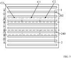
- Figure 5 shows a schematic top view of a corresponding semiconductor structure.
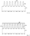
- Figure 6 shows a schematic cross-section view of the semiconductor structure shown in Figure 5 along line "1-2".
- a base structure may be formed.
- the base structure may include an isolation region A, a device region B, and a transition region C separating the isolation region A from the device region B.
- the base structure may also include a plurality of fin structures 202 formed on a substrate 201 in the device region B, and a plurality of initial fin structures 240 formed on the substrate 201 in the transition region C and the isolation region A.
- the device region B includes two discrete sub-regions
- the transition region C also includes two discrete sub-regions.
- each sub-region of the device region B is separated from the isolation region A by a sub-region of the transition region C.
- the isolation region, the device region, and the transition region may each include a plurality of sub-regions as long as each sub-region of the device region is separated from the isolation region by the sub-regions of the transition region.
- each of the isolation region, the device region, and the transition region may only include one sub-region.
- each sub-region of the transition region C may include a dummy gate region C1 and a pair of dummy source/drain regions C2 separated by the dummy gate region C1.
- the two side edges of the dummy gate region C1 may be in contact with the isolation region A and the device region B, respectively.
- the isolation region A may be used to electrically isolate neighboring sub-regions of the device region B.
- the transition region C may be used to electrically isolate the isolation region A from the device region B, and thus provide protection for the portion of the fin structures 202 formed in the device region B.
- the dummy gate region C1 may be used to form a plurality of dummy gate structures in a subsequent process.
- the substrate 201, the plurality of fin structures 202, and the plurality of initial fin structures 240 may be made of a same material.
- the substrate 201, the plurality of fin structures 202, and the plurality of initial fin structures 240 may be made of silicon.
- the substrate, the fin structures, as well as the initial fin structures may also be made of germanium, SiGe, silicon on insulator (SOI), germanium on insulator (GOI), or any other appropriate semiconductor materials.
- the initial substrate may be patterned by a dry etching process.
- the etching effect of the dry etching process may be isotropic, and thus the sidewall surfaces of the fin structures 202 and the initial fin structures 240 may be perpendicular to the substrate 201 as desired.
- the initial substrate may be patterned by a wet etching process or by a process combining dry etching and wet etching.
- the portion of the initial fin structures 240 formed on the substrate 201 in the isolation region A and the dummy source/drain regions C2 may be remove such that only the portion of the initial fin structures 240 formed on the substrate 201 in the dummy gate region C1 may be retained to form a plurality of dummy fin structures.
- an isolation material layer may be formed on the substrate in the isolation region, the device region, and the transition region with a top surface of the isolation material layer higher than the top surfaces of the plurality of fin structures (S1102).
- Figure 7 shows a schematic cross-section view of a corresponding semiconductor structure.
- an isolation material layer 211 may be formed on the substrate 201 in the isolation region A, the device region B, and the transition region C.
- the top surface of the isolation material layer 211 may be higher than the top surfaces of the plurality of fin structures 202.
- the isolation material layer 211 may be used to form a second isolation layer in a subsequent process.
- the second isolation layer may be used to electrically isolate the neighboring fin structures 202 in the device region B.
- the isolation material layer 211 may be made of SiO x . In other embodiments, the isolation material layer may also be made of SiON.
- the isolation material layer 211 may be formed by a fluid CVD process. Specifically, the isolation material layer 211 formed by a fluid CVD process may demonstrate desired gap-filling ability such that the insulation property of the subsequently-formed second initial isolation layer may be desired.
- the portion of the initial fin structures and the isolation material layer formed in the isolation region may be removed to form a first trench, the portion of the initial fin structures and the isolation material layer formed in each dummy source/drain region may be removed to form a second trench, and accordingly, the remaining portion of the initial fin structures in the dummy gate region may become a plurality of dummy fin structures, while the remaining portion of the isolation material layer in the dummy gate region and the device region may become a second initial isolation layer covering the fin structures and the dummy fin structures (S1103).
- Figure 8 shows a schematic top view of a corresponding semiconductor structure.
- Figure 9 shows a schematic cross-section view of the semiconductor structure shown in Figure 8 along line "3-4”
- Figure 10 shows a schematic cross-section view of the semiconductor structure shown in Figure 8 along line "5-6".
- the portion of the initial fin structures 240 (referring to Figure 7 ) and the portion of the isolation material layer 211 (referring to Figure 7 ) formed in the isolation region A may be removed to form a first trench 210 in the isolation region A, while the portion of the initial fin structures 240 and the portion of the isolation material layer 211 formed in each dummy source/drain region C2 may be removed to form a second trench 214 in the corresponding dummy source/drain region C2. Accordingly, the remaining portion of the initial fin structures 240 formed in the dummy gate structure C1 may become a plurality of dummy fin structures 241. Moreover, the remaining portion of the isolation material layer 211 formed on the substrate 201 in the dummy gate region C1 and the device region B may become a second initial isolation layer 212 that covers the fin structures 202 and the dummy fin structures 241.
- the first trench 210 and each second trench 214 may be filled with a first isolation layer in a subsequent process.
- the dummy fin structures 241 may be used to electrically isolate the fin structures in the device region B from the isolation region A.
- the second initial isolation layer may be used to form a second isolation layer in a subsequent process.
- the dummy fin structures 241 may not be formed on the substrate 201 in the dummy source/drain regions C2, and thus further formation of transistors in the dummy source/drain regions C2 from the dummy fin structures 241 may be avoided. Therefore, the influence of the fin width of the dummy fin structures 241 on the performance of the formed semiconductor structure may be reduced.
- the process to remove the portion of the initial fin structures 240 and the isolation material layer 211 formed in the isolation region A and the dummy source/drain regions C2 may include the following steps. First, a patterned layer may be formed on the isolation material layer 211. The patterned layer may expose the surface of the portion of the isolation material layer 211 formed in the isolation region A and the dummy source/drain regions C2. Further, the isolation material layer 211 and the initial fin structures 240 may be etched using the patterned layer as an etch mask to form the first trench 210 and the second trench 214.
- a plurality of initial fin structures 240 may be formed in the dummy gate region C1
- the portion of the initial fin structures 240 in the dummy gate region C1 may be able to prevent the etch gas from reaching the portion of the fin structures 202 formed in the device region B. Therefore, the width of the portion of the fin structures 202 adjacent to the dummy gate region C1 may not be easily reduced, and hence the uniformity of the width of the fin structures 202 may be ensured.
- the dummy fin structures 241 and the fin structures 202 may be made of a same material.
- the dummy fin structures 241 and the fin structures 202 may both be made of silicon.
- the dummy fin structures 241 may also be made of germanium, SiGe, or any other appropriate material.
- the dummy fin structures 241 and the fin structures 202 are made of a same material, during the process to etch the initial fin structures 240, the dummy fin structures 241 may be able to react with the etching reactant so that the amount of the etching reactant reaching the fin structures 202 adjacent to the transition region C may be reduced. Therefore, reduction of the width of the fin structures 202 formed adjacent to the transition region C may be suppressed, ensuring the uniformity of the width of the fin structures 202.
- the fin structures and the dummy fin structures may also be made of different materials.
- the isolation material layer 211 and the initial fin structures 240 may be etched by a dry etching process. Specifically, the etching effect of the dry etching process is isotropic so that the damage to the sidewalls of the first trench 210 and the second trench 214 may be limited. In other embodiments, the isolation material layer and the initial fin structures may also be etched by a wet etching process or by a process combining dry etching and wet etching.
- each dummy fin structure 241 and each fin structure 202 may have an identical fin width. In other embodiments, the width of each dummy fin structure 241 and the width of each fin structure 202 may be different.
- a first initial isolation layer may be formed in the first trench and the second trench (S1104).
- Figure 11 shows a schematic cross-section view of a corresponding semiconductor structure developed from the structure shown in Figure 9
- Figure 12 shows a schematic cross-section view of a corresponding semiconductor structure developed from the structure shown in Figure 10 .
- a first initial isolation layer 220 may be formed to fill the first trench 210 (referring to Figure 10 ) and the second trench 214 (referring to Figure 9 ).
- the first initial isolation layer 220 may be used to form a first isolation layer in a subsequent process.
- the first initial isolation layer 220 and the second initial isolation layer 212 may be made of a same material.
- the first initial isolation layer 220 and the second initial isolation layer 212 may be made of SiO x .
- the first initial isolation layer may be made of SiON.
- the first initial isolation layer 220 and the second initial isolation layer 212 are made of a same material, and thus a single etching process may be performed to etch both the first initial isolation layer 220 and the second initial isolation layer 212. As such, the fabrication process may be simplified and the product yield may also be improved. In other embodiments, the second initial isolation layer and the first initial isolation layer may be made of different materials.
- the first initial isolation layer 220 may be formed by a fluid CVD process.
- the fluid CVD process adapted to form the first initial isolation layer may include the following steps. First, a precursor may be formed in the first trench 210 and the second trench 214. The precursor may be a fluid so that the first trench 210 and the second trench 214 may be efficiently filled by the precursor. Then, an annealing process may be performed to activate the precursor and thus form the first initial isolation layer 220.
- the precursor may be a material containing carbon-hydrogen bonds, carbon-oxygen bonds, and nitrogen-silicon bonds.
- the reactant used in the annealing process to anneal the precursor may be an oxygen-containing gas such as water vapor, oxygen gas, etc.
- the oxygen atoms in the oxygen-containing gas may replace the nitrogen atoms and hydrogen atoms in the precursor, and form the first initial isolation layer 220.
- the oxygen-containing gas may easily diffuse. Because of the presence of the transition region C between the device region B and the isolation region A and the dummy fin structures 241 on the substrate 201 in the dummy gate region C1, the oxygen-containing gas may not be able to easily reach the fin structures 202 formed in the device region B due to the blocking effect of the dummy fin structures 241. Therefore, the uniformity of the width of the fin structures 202 in the device region B may be ensured, and thus the performance of the formed semiconductor structure may be improved.
- the first initial isolation layer 220 may also be formed on the second initial isolation layer 212.
- a first isolation layer and a second isolation layer may be formed by etching the first initial isolation layer and the second initial isolation layer until the top surface of the second initial isolation layer becomes lower than the top surfaces of the fin structures (S1105).
- Figure 13 shows a schematic top view of a corresponding semiconductor structure.
- Figure 14 shows a schematic cross-section view of the semiconductor structure shown in Figure 13 along line "7-8" and
- Figure 15 shows a schematic cross-section view of the semiconductor structure shown in Figure 13 along line "9-0" .
- an etching process may be performed to etch the second initial isolation layer 212 (referring to Figure 12 ) and the first initial isolation layer 220 (referring to Figure 12 ). With the top surfaces of the first initial isolation layer 220 and the second initial isolation layer 212 become lower than the top surfaces of the fin structures 202, a first isolation layer 221 and a second isolation layer 213 may be formed.
- the second isolation layer 213 may be used to electrically isolate neighboring fin structures 202 and the first isolation layer 221 may be used to electrically isolate different sub-regions of the device region B.
- the first isolation layer 221 and the second isolation layer 213 may together form an isolation structure.
- the fabrication process may also include removing the portion of the first initial isolation layer 220 formed on the second initial isolation layer 212.
- the portion of the first initial isolation layer 220 formed on the second initial isolation layer 212 may be removed by a chemical mechanical polishing process, a dry etching process, or a wet etching process.
- the process to etch the second initial isolation layer 212 and the first initial isolation layer 220 may include dry etching or wet etching.
- the portion of the initial fin structures 212 formed in the isolation region A may be removed.
- the first isolation layer 221 may then be formed in the first trench 210 and the second trench 214. As such, the thickness of the formed first isolation layer 221 may be uniform. Therefore, the isolation properties of the first isolation layer 221 may be ensured, and the performance of the formed semiconductor device may be improved.
- a plurality of gate structures may be formed across the fin structures in the device region (S1106).
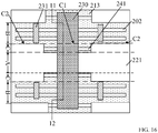
- Figure 16 shows a schematic top view of a corresponding semiconductor structure developed from the structure shown in Figure 13 .
- Figure 17 shows a schematic cross-section view of the semiconductor structure shown in Figure 16 along line "11-12".
- a plurality of gate structures 230 may be formed across the fin structures 202 in the device region B.
- the plurality of gate structures 230 may cover a portion of the sidewall and the top surfaces of each fin structure 202.
- the gate structure 230 may also be formed across the plurality of dummy fin structures 241. In addition, a portion of the gate structure 230 may be formed on the surface of the first isolation layer 221.
- each gate structure 230 may include a gate dielectric layer formed across the plurality of fin structures 202 and a gate electrode formed on the gate dielectric layer.
- the gate dielectric layer may cover a portion of the sidewall and the top surfaces of each fin structure 202.
- the gate dielectric layer may be made of SiO x .
- the gate dielectric layer may also be made of a high-k (k > 3.9) dielectric material including HfO 2 , La 2 O 3 , HfSiON, HfAlO 2 , ZrO 2 , Al 2 O 3 , HfSiO 4 , etc.
- the gate electrode may be made of polycrystalline silicon. In other embodiments, the gate electrode may also be made of a metal, including Al, Cu, Ag, Au, Ni, Ti, W, WN, WSi, etc.
- two doped source/drain regions may be formed in the fin structures on the two opposite sides of each gate structure in the device region (S1107).
- two doped source/drain regions 231 may be formed in the fin structures 202 on the two opposite sides of the gate electrode.
- the process to form the doped source/drain regions 231 may include forming two trenches in the fin structures 202 on the two opposite sides of the gate structure 230 in the device region B and then forming the two doped source/drain regions 231 in the two trenches.
- the two doped source/drain regions 231 may be formed in the two trenches formed in the device region B through an epitaxial growth process.
- each dummy source/drain region C2 may be covered by the first isolation layer 221, during the epitaxial growth process to form the doped source/drain regions 231, the doped source/drain regions 231 may not be formed on the two opposite sides of the gate structures 230 in each dummy gate region C1. Therefore, semiconductor devices incorporating the dummy fin structures 241 may not be formed, and thus the width of the dummy fin structures 241 may not be able to affect the performance of the formed semiconductor structure.
- MOS metal-oxide-semiconductor
- the dummy fin structures may be formed on the substrate in the transition region and the semiconductor device may include an N-type epitaxial layer formed on the fin structures in the first device region and a P-type epitaxial layer formed on the fin structures in the second device region.
- the N-type epitaxial layer may include N-type doping ions and the P-type epitaxial layer may include P-type doping ions.
- the conduction types of the P-type doping ions and the N-type doping ions may be different, and the P-type epitaxial layer and the N-type epitaxial layer may be in contact with each other.
- the dummy fin structures in the transition region may be exposed by the P-type epitaxial layer and the N-type epitaxial layer.
- the present invention also provides another method for fabricating a semiconductor structure.
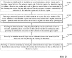
- Figure 25 shows a flowchart of another exemplary method for fabricating a semiconductor structure consistent with various disclosed embodiments in the present invention.
- Figures 18-23 show schematic cross-section views of semiconductor structures at certain stages of the exemplary method.
- an initial substrate including an isolation region, a device region, and a transition region formed between the isolation region and the device region may be provided, and the transition region includes a dummy gate region and a pair of dummy source/drain regions separated by the dummy gate region (S2101).
- Figure 18 shows a schematic top view of a corresponding semiconductor structure.
- an initial substrate 300 may be provided.
- the initial substrate 300 may include an isolation region M, a device region K, and a transition region N between the isolation region M and the device region K.
- the device region K includes two discrete sub-regions
- the transition region N may also include two discrete sub-regions.
- each sub-region of the device region K is separated from the isolation region M by a sub-region of the transition region N.
- the isolation region, the device region, and the transition region may each include a plurality of sub-regions as long as each sub-region of the device region is separated from the isolation region by the sub-regions of the transition region.
- each of the isolation region, the device region, and the transition region may only include one sub-region.
- the transition region N may include one dummy gate region N1 and a pair of dummy source/drain regions N2 formed on the two opposite sides of the dummy gate region N1.
- a patterned layer may be formed on the initial substrate to expose the entire portion of the initial substrate in the isolation region and each dummy source/drain region and also expose a portion of the initial substrate in the device region and the dummy gate region (S2102).
- the position of the exposed portion of the initial substrate is schematically shown in Figure 19 .
- a portion of the initial substrate 300 may be exposed by a patterned layer (not shown) formed on the initial substrate 300.
- the patterned layer may not cover the entire portion of the substrate 300 in the isolation region M and the dummy source/drain regions N2. Moreover, the patterned layer may also expose a portion of the initial substrate 300 in the device region K and the dummy gate region N1.
- the patterned layer may be used to define the widths and the positions for subsequently-formed fin structures and dummy fin structures. Specifically, the portion of the initial substrate 300 in the device region K covered by the patterned layer may define the top surfaces of subsequently-formed fin structures in the device region K, and the portion of the initial substrate 300 in the dummy gate region N1 covered by the patterned layer may define the top surfaces of subsequently-formed dummy fin structures in the dummy gate region N1.
- the patterned layer may be a patterned hard mask. In other embodiments, the patterned layer may also be a photoresist layer or an anti-reflective layer.
- the hard mask layer may be made of SiO x . In other embodiments, the hard mask layer may be made of SiON.
- an etching process using the patterned layer as an etch mask may be performed on the initial substrate to form a substrate, a plurality of fin structures on the substrate in the device region, and a plurality of dummy fin structures on the substrate in the dummy gate region (S2103).
- Figure 19 shows a schematic top view of the corresponding semiconductor substrate with a substrate, a plurality of fin structures, and a plurality of dummy fin structures formed from the initial substrate.
- Figure 20 shows a schematic cross-section view of the structure shown in Figure 19 along line "21-22" with an isolation material layer formed on the top.
- Figure 21 shows a schematic cross-section view of the structure shown in Figure 19 along line "23-24" with an isolation material layer formed on the top.
- the initial substrate 300 (referring to Figure 18 ) may be etched using the patterned layer as an etch mask. After the etching process, a substrate 301, a plurality of fin structures 302, and a plurality of dummy fin structures 303 may be formed from the initial substrate 300.
- the plurality of fin structures 302 may be formed on the substrate 301 in the device region K, and the plurality of dummy fin structures 303 may be formed on the substrate 301 in the dummy gate region N1.
- the initial substrate 300 may be etched through a dry etching process. Specifically, such a dry etching process may demonstrate anisotropic etching effect and desired profile control. Therefore, the sidewalls of the fin structures 302 and the dummy fin structures 303 formed by a dry etching process may be perpendicular to the surface of the substrate 301 as desired.
- the initial substrate may also be etched through a wet etching process or a process combining dry etching and wet etching.
- a plurality of dummy fin structures 203 may be formed on the substrate 301 in the dummy gate region N1. Further, the plurality of dummy fin structures 303 may prevent compounds produced during the process to etch the portion of the initial substrate 300 in the isolation region M from reaching the fin structures 302 formed in the adjacent device region K. Therefore, increase in the width of the fin structures 302 in the adjacent device region K during the etching process may be avoided. As such, the uniformity of the fin width of the fin structures 302 in the may be ensured, and thus the formation method may improve the performance of the formed semiconductor structure.
- a plurality of dummy fin structures 303 may be formed on the substrate 301 in the dummy gate region N1. Further, during the process to etch the initial substrate 300, the plurality of dummy fin structures 303 may prevent the reactant from reaching the fin structures 302 formed in the adjacent device region K. Therefore, the influence of the reactant on the width of the fin structures 302 in the device region K may be reduced, and thus the uniformity of the fin width of the fin structures 302 may be improved.
- the fabrication process may be simplified.
- an isolation material layer covering the plurality of fin structures and the plurality of dummy fin structures may be formed on the substrate (S2104).
- Figures 20-21 show schematic views of a corresponding semiconductor structure.
- an isolation material layer 320 may be formed on the substrate 301 in the isolation region M, the device region K, as well as the transition region N.
- the top surface of the isolation material layer 320 may be higher than the top surfaces of the plurality of fin structures 302 and the plurality of dummy fin structures 303. That is, the isolation material layer 320 may cover the top and sidewall surfaces of the fin structures 302 and the dummy fin structures 303.
- the isolation material layer 320 may be used to form a first isolation layer and a second isolation layer in a subsequent process.
- the isolation material layer 320 may be made of SiO x . In other embodiments, the isolation material layer may be made of SiON.
- the isolation material layer 320 may be fabricated by a CVD process. Moreover, forming the isolation material layer 320 through a CVD process may further include forming a precursor on the substrate 301 in the isolation region M, the device region K, and the transition region N, and then performing an annealing process to activate the precursor and thus form the isolation material layer 320.
- the precursor may be flowable, e.g., in form of a fluid. Therefore, the formed isolation material layer 320 may be able to fully fill the gaps between neighboring fin structures 302 in the device region K. As such, the formed isolation material layer 320 may demonstrate desired isolation property.
- the precursor may be a material containing carbon-hydrogen bonds, carbon-oxygen bonds, and nitrogen-silicon bonds.
- the reactant used in the annealing process to anneal the precursor may be an oxygen-containing gas including water vapor, oxygen gas, etc.
- the oxygen atoms in the oxygen-containing gas may replace the nitrogen atoms and hydrogen atoms in the precursor, and thus form the isolation material layer 320.
- the portion of the isolation material layer 320 formed on the substrate 301 in the isolation region M may have a large area. Therefore, during the annealing process, the concentration of the oxygen-containing gas reaching the substrate 301 in the isolation region may be high, and thus the oxygen-containing gas may easily diffuse. Because of the presence of the transition region N between the device region K and the isolation region M and the formation of the dummy fin structures 303 on the substrate 301 in the dummy gate region N1, the oxygen-containing gas may not be able to easily reach the fin structures 302 formed in the device region K due to the blocking effect of the dummy fin structures 303. Therefore, the uniformity of the fin width of the fin structures 302 in the device region K may be ensured, and thus the performance of the formed semiconductor structure may be improved.
- the dummy fin structures 303 may be made of silicon.
- the dummy fin structures 303 may react with the oxygen-containing gas such that the amount of the oxygen-containing gas reaching the fin structures 302 in the device region K may be reduced. Therefore, reduction of the width of the fin structures 302 adjacent to each transition region N may be suppressed.
- an isolation structure may be formed by etching the isolation material layer until the surface of the isolation material layer becomes lower than the top surfaces of the fin structures in the device region (S2105).
- Figures 22-23 show schematic cross-section views of a corresponding semiconductor structure. Specifically, Figure 22 shows a schematic cross-section view developed from the cross-section view shown in Figure 20 , and Figure 23 shows a schematic cross-section view developed from the cross-section view shown in Figure 21 .
- the isolation material layer 320 (referring to Figures 20-21 ) may be etched until the top surface of the isolation material layer 320 becomes lower than the top surfaces of the fin structures 302 in the device region K. As such an isolation structure 321 may be formed.
- the isolation material layer 320 may be etched by a dry etching process or a wet etching process.
- a plurality of dummy fin structures may be formed on the substrate in the transition region. Further, during the process to form a plurality of fin structures or form a first isolation layer, the dummy fin structures may prevent the reactant and the produced compound from reaching the fin structures in the adjacent device region. As such, during the process to form the fin structures or form the first isolation layer, the influence of the reactant and the produced compound on the width of the fin structures in the device regions may be reduced. Therefore, the uniformity of the fin width may be ensured, and thus the disclosed fabrication method may improve the performance of the formed semiconductor structure.
- the first isolation layer may cover the portion of the substrate in the dummy source/drain regions, and thus the dummy fin structures may not be formed in the dummy source/drain regions. Therefore, forming transistors from the dummy fin structures in the dummy source/drain regions may be avoided. As a result, the influence of the width of the dummy fin structures on the performance of the formed semiconductor devices may be reduced.
- the initial substrate may be patterned to form the plurality of fin structures and the plurality of dummy fin structures, and then the first isolation layer and the second isolation layer may be formed. As such, the fabrication process may be simplified and the product yield may be improved.
- the present invention also provides a semiconductor structure.
- Figure 16 shows a schematic top view of an exemplary semiconductor structure consistent with various embodiments of the present invention.
- Figure 17 shows the schematic cross-section view of the structure shown in Figure 16 along line "11-12".
- the semiconductor structure may include an isolation region A, a device region B, and a transition region C between the isolation region A and the device region B.
- the semiconductor structure may include a plurality of fin structures 202 formed on a substrate 201 in the device region B, a plurality of dummy fin structures 241 formed on the substrate 201 in the transition region C, and an isolation structure formed on the substrate 201 in the isolation region A, the device region B, and the transition region C.
- the semiconductor structure may also include a plurality of semiconductor devices formed on the fin structures 202 in the device region B.
- the device region B includes two discrete sub-regions
- the transition region C includes two discrete sub-regions.
- each sub-region of the device region B is separated from the isolation region A by a sub-region of the transition region C.
- the isolation region, the device region, and the transition region may each include a plurality of sub-regions as long as each sub-region of the device region is separated from the isolation region by the sub-regions of the transition region.
- each of the isolation region, the device region, and the transition region may only include one sub-region.
- the isolation region A may be used to electrically isolate neighboring sub-regions of the device region B. Further, the transition region C may be used to form the plurality of dummy fin structures 241 to provide protection for the plurality of fin structures 202 in the device region B during the fabrication process.
- each sub-region of the transition region C may include a dummy gate region C1 and a pair of dummy source/drain regions C2 separated by the dummy gate region C1.
- the two side edges of the dummy gate region C1 may be in contact with the isolation region A and the device region B, respectively.
- the transition region may not include the dummy gate region.
- the plurality of dummy fin structures 241 may be formed on the substrate 201 in the dummy gate region C1. In other embodiments, the dummy fin structures may also be formed on the substrate in the dummy source/drain regions.
- the isolation region A may electrically isolate the sub-regions of the device region B. Further, each transition region C may electrically isolate the isolation region A from the device region B, and thus provide protection for the fin structures formed in the device region B.
- the substrate 201, the plurality fin structures 202, and the plurality of dummy fin structures 241 may be made of a same material.
- the substrate 201, the plurality fin structures 202, and the plurality of dummy fin structures 241 may be made of silicon.
- the substrate 201, the plurality fin structures 202, and the plurality of dummy fin structures 241 may be made of germanium, SiGe, silicon on insulator (SOI), germanium on insulator (GOI), or any other appropriate material.
- a plurality of dummy fin structures 241 may be formed on the substrate 201 in the dummy gate region C1.
- the plurality of dummy fin structures 241 may isolate the adjacent fin structures 202 in the device region B from the isolation region A, and thus provide protection for the fin structures 202 in the device region B. Therefore, change in the width of the fin structures 202 in the device region B may be suppressed. As such, the uniformity of the width of the fin structures 202 in the semiconductor structure may be improved and the performance of the formed semiconductor structure may also be improved.
- the dummy fin structures 241 may not be formed on the substrate 201 in the dummy source/drain regions C2 such that forming transistors from the dummy fin structures 241 in the dummy source/drain regions C2 may be avoided. Therefore, the influence of the width of the dummy fin structures 241 on the performance of the formed semiconductor structure may be reduced.
- the plurality of fin structures 202 and the plurality of dummy fin structures 241 may be made of a same material. As such, the plurality of dummy fin structures 241 may easily react with the reactant gas which reacts with the fin structures 202 and affects the fin width of the fin structures 202. Therefore, the presence of the plurality of dummy fin structures 241 may prevent the reactant gas from reaching the fin structures 202 in the transition region C. With the amount of the reactant gas reaching the fin structures 202 in the transition region C reduced, reduction of the width of the fin structures 202 in the transition region C may be suppressed, and thus the uniformity of the width of the fin structures 202 may be ensured.
- the fin structures and the dummy fin structures may be made of different materials.
- the number of the dummy fin structures 241 may be one or more than one.
- the isolation structure may include a first isolation layer 221 formed on the portion of the substrate 201 in the isolation region A and the dummy source/drain regions C1, and a second isolation layer 213 formed on the portion of the substrate 201 in the device region B and the dummy gate region C1. Moreover, the top surface of the second isolation region 213 may be below the top surfaces of the fin structures 202.
- the second isolation layer 213 may be used to electrically isolate neighboring fin structures 202, while the first isolation layer 221 may be used to electrically isolate neighboring sub-regions of the device region B.
- the first isolation layer 221 and the second isolation layer 213 may be formed by a same material.
- the first isolation layer 221 and the second isolation layer 213 may be both formed by SiO x .
- the first isolation layer and the second isolation layer may be made of different materials.
- the semiconductor structure may further include a plurality of gate structures 230 formed across the plurality of fin structures 202 in the device region B and two doped source/drain regions 231 formed in the fin structures 202 on the two opposite sides of each gate structure 230 in the device region B.
- each gate structure 230 may cover a portion of the top and the sidewall surfaces of the fin structures 202 in the device region B.
- the transition region may not include the dummy gate region; accordingly, the semiconductor structure may not include the gate structures.
- the gate structures 230 may also be formed across the plurality of dummy fin structures 241. In addition, a portion of the gate structures 230 may be formed on the surface of the first isolation layer 221.
- each gate structure 230 may further include a gate dielectric layer formed across the plurality of fin structures and a gate electrode formed on the gate dielectric layer.
- the gate dielectric layer may cover a portion of the top and the sidewall surfaces of the fin structures 202.
- the gate dielectric layer may be made of SiO x .
- the gate dielectric layer may be made of a high-k (k > 3.9) dielectric material including HfO 2 , La 2 O 3 , HfSiON, HfAlO 2 , ZrO 2 , Al 2 O 3 , HfSiO 4 , etc.
- the gate electrode may be made of polycrystalline silicon. In other embodiments, the gate electrode may also be made of a metal, including Al, Cu, Ag, Au, Ni, Ti, W, WN, WSi, etc.
- the doped source/drain regions 231 may not be formed on the two opposite sides of the gate structures 230 in the dummy gate region C1. Therefore, semiconductor devices incorporating the dummy fin structures 241 may not be formed, and thus the width of the dummy fin structures 241 may not be able to affect the performance of the formed semiconductor structure.
- the disclosed semiconductor structure is illustrated based on structures of metal-oxide-semiconductor (MOS) transistors, with a plurality of dummy fin structures formed on the substrate in the transition region, the semiconductor structure may also be diodes or triodes.
- MOS metal-oxide-semiconductor
- the semiconductor device may include an N-type epitaxial layer formed on the fin structures in the first sub-region of the device region and a P-type epitaxial layer formed on the fin structures in the second sub-region of the device region.
- the N-type epitaxial layer may include N-type doping ions and the P-type epitaxial layer may include P-type doping ions.
- the conduction types of the P-type doping ions and the N-type doping ions may be different and the P-type epitaxial layer and the N-type epitaxial layer may be in contact with each other.
- the dummy fin structures in the transition region may be exposed by the P-type epitaxial layer and the N-type epitaxial layer.
- the disclosed fabrication methods and semiconductor structures may demonstrate several advantages.
- a plurality of dummy fin structures may be formed on the substrate in the transition region. Further, during the process to form a plurality of fin structures or form a first isolation layer, the dummy fin structures may prevent the reactant and the produced compound from reaching the fin structures in the adjacent device region. As such, during the process to form the fin structures or form the first isolation layer, the influence of the reactant and the produced compound on the width of the fin structures in the device region may be reduced or eliminated. Therefore, the uniformity of the fin width may be ensured, and thus the disclosed fabrication method may improve the performance of the formed semiconductor structure.
- the first isolation layer may cover the portion of the substrate in the dummy source/drain regions, and thus the dummy fin structures may not be formed in the dummy source/drain regions. Therefore, forming transistors from the dummy fin structures in the dummy source/drain regions may be avoided. As a result, the influence of the width of the dummy fin structures on the performance of the formed semiconductor devices may be reduced.
- the initial substrate may be patterned to form the plurality of fin structures and the plurality of dummy fin structures, and then the first isolation layer and the second isolation layer may be formed. As such, the fabrication process may be simplified and the product yield may be improved.
- the portion of the initial fin structures formed in the isolation region may be removed and then a first isolation layer may be formed in the first trench and the second trench. Therefore, the uniformity of the thickness of the first isolation layer in the isolation region may be ensured. As such, the isolation properties of the first isolation layer may be ensured and the performance of the formed semiconductor structure may be improved.
- the plurality of fin structures and the plurality of dummy fin structures may be made of a same material.
- the plurality of dummy fin structures may easily react with the reactant gas which reacts with the fin structures and affects the fin width of the fin structures. Therefore, the presence of the plurality of dummy fin structures may prevent the reactant gas from reaching the fin structures in the transition region. With the amount of the reactant gas reaching the fin structures in the transition region reduced, reduction of the width of the fin structures in the transition region may be suppressed, and thus the uniformity of the width of the fin structures may be improved.
- first initial isolation layer and the second initial isolation layer may be made of a same material, and thus the first initial isolation layer and the second initial isolation layer may be etched by a single etching process. Therefore, the fabrication process may be simplified and the product yield may also be improved.
- a plurality of dummy fin structures may be formed on the substrate in the transition region.
- the dummy fin structures may isolate the fin structures in the adjacent device region from the isolation region, and thus provide protection for the fin structures in the device region.
- change in the fin width of the fin structures in the device region may be suppressed. Therefore, the uniformity of the fin width of the fin structures in the formed semiconductor structure may be improved, and the performance of the formed semiconductor structure may also be improved.
- the first isolation layer may cover the portion of the substrate in the dummy source/drain regions.
- the dummy fin structures may not be formed on the substrate in the source/drain regions. Therefore, forming transistors from the dummy fin structures in the dummy source/drain regions may be avoided, and the influence of the width of the dummy fin structures on the semiconductor structure may be reduced.
Landscapes
- Insulated Gate Type Field-Effect Transistor (AREA)
- Engineering & Computer Science (AREA)
- Physics & Mathematics (AREA)
- Plasma & Fusion (AREA)
- General Engineering & Computer Science (AREA)
- Chemical & Material Sciences (AREA)
- Chemical Kinetics & Catalysis (AREA)
- General Chemical & Material Sciences (AREA)
Applications Claiming Priority (1)
| Application Number | Priority Date | Filing Date | Title |
|---|---|---|---|
| CN201610876700.6A CN107887272B (zh) | 2016-09-30 | 2016-09-30 | 半导体结构及其形成方法 |
Publications (1)
| Publication Number | Publication Date |
|---|---|
| EP3301708A1 true EP3301708A1 (de) | 2018-04-04 |
Family
ID=60001733
Family Applications (1)
| Application Number | Title | Priority Date | Filing Date |
|---|---|---|---|
| EP17194073.7A Withdrawn EP3301708A1 (de) | 2016-09-30 | 2017-09-29 | Halbleiterstrukturen und herstellungsverfahren dafür |
Country Status (3)
| Country | Link |
|---|---|
| US (1) | US10177145B2 (de) |
| EP (1) | EP3301708A1 (de) |
| CN (1) | CN107887272B (de) |
Families Citing this family (20)
| Publication number | Priority date | Publication date | Assignee | Title |
|---|---|---|---|---|
| CN107799421B (zh) * | 2016-09-05 | 2021-04-02 | 中芯国际集成电路制造(上海)有限公司 | 半导体器件的形成方法 |
| US10403714B2 (en) * | 2017-08-29 | 2019-09-03 | Taiwan Semiconductor Manufacturing Co., Ltd. | Fill fins for semiconductor devices |
| US10325912B2 (en) | 2017-10-30 | 2019-06-18 | Taiwan Semiconductor Manufacturing Co., Ltd. | Semiconductor structure cutting process and structures formed thereby |
| CN109786458B (zh) * | 2017-11-13 | 2022-02-15 | 中芯国际集成电路制造(上海)有限公司 | 半导体器件及其形成方法 |
| TWI750316B (zh) * | 2018-02-09 | 2021-12-21 | 聯華電子股份有限公司 | 1-1強制性鰭狀堆疊反向器及形成強制性鰭狀堆疊反向器的方法 |
| US11056394B2 (en) * | 2018-06-28 | 2021-07-06 | Taiwan Semiconductor Manufacturing Co., Ltd. | Methods for fabricating FinFETs having different fin numbers and corresponding FinFETs thereof |
| CN110858545B (zh) * | 2018-08-24 | 2023-04-25 | 中芯国际集成电路制造(上海)有限公司 | 半导体结构及其形成方法 |
| US11056393B2 (en) | 2018-09-27 | 2021-07-06 | Taiwan Semiconductor Manufacturing Co., Ltd. | Method for FinFET fabrication and structure thereof |
| US10818556B2 (en) * | 2018-12-17 | 2020-10-27 | United Microelectronics Corp. | Method for forming a semiconductor structure |
| CN111370488B (zh) * | 2018-12-26 | 2024-04-16 | 中芯国际集成电路制造(北京)有限公司 | 半导体结构及其形成方法 |
| US11011626B2 (en) * | 2019-05-07 | 2021-05-18 | International Business Machines Corporation | Fin field-effect transistor with reduced parasitic capacitance and reduced variability |
| CN112086401B (zh) * | 2019-06-12 | 2024-12-17 | 中芯国际集成电路制造(上海)有限公司 | 半导体器件及其形成方法 |
| CN112133633B (zh) * | 2019-06-25 | 2024-11-19 | 中芯国际集成电路制造(上海)有限公司 | 半导体器件及其形成方法 |
| CN112635560B (zh) * | 2019-10-08 | 2023-12-05 | 联华电子股份有限公司 | 鳍状晶体管结构及其制造方法 |
| CN113496894B (zh) * | 2020-04-01 | 2024-04-19 | 中芯国际集成电路制造(上海)有限公司 | 半导体结构的形成方法 |
| CN113658864B (zh) * | 2020-05-12 | 2024-12-17 | 中芯国际集成电路制造(上海)有限公司 | 半导体结构的形成方法 |
| US11538815B2 (en) * | 2020-07-22 | 2022-12-27 | Globalfoundries U.S. Inc. | Non-volatile memory cell arrays with a sectioned active region and methods of manufacturing thereof |
| CN114005754A (zh) * | 2020-07-28 | 2022-02-01 | 中芯南方集成电路制造有限公司 | 半导体结构及其形成方法 |
| CN112349722B (zh) * | 2020-10-15 | 2021-11-09 | 长江存储科技有限责任公司 | 半导体器件结构及其制备方法 |
| CN114823338A (zh) * | 2021-01-22 | 2022-07-29 | 中芯国际集成电路制造(上海)有限公司 | 半导体结构的形成方法 |
Citations (4)
| Publication number | Priority date | Publication date | Assignee | Title |
|---|---|---|---|---|
| US20140203376A1 (en) * | 2013-01-18 | 2014-07-24 | Globalfoundries Inc. | Finfet integrated circuits with uniform fin height and methods for fabricating the same |
| US20150147874A1 (en) * | 2013-11-25 | 2015-05-28 | United Microelectronics Corp. | Method for forming a semiconductor structure |
| US20150206759A1 (en) * | 2014-01-21 | 2015-07-23 | United Microelectronics Corp. | Semiconductor structure and manufacturing method thereof |
| US20150311311A1 (en) * | 2014-04-25 | 2015-10-29 | Semiconductor Manufacturing International (Shanghai) Corporation | Static memory cell and formation method thereof |
Family Cites Families (4)
| Publication number | Priority date | Publication date | Assignee | Title |
|---|---|---|---|---|
| US8697515B2 (en) * | 2012-06-06 | 2014-04-15 | Taiwan Semiconductor Manufacturing Company, Ltd. | Method of making a FinFET device |
| US9281382B2 (en) * | 2014-06-04 | 2016-03-08 | Stmicroelectronics, Inc. | Method for making semiconductor device with isolation pillars between adjacent semiconductor fins |
| US9397099B1 (en) * | 2015-01-29 | 2016-07-19 | Taiwan Semiconductor Manufacturing Co., Ltd. | Semiconductor device having a plurality of fins and method for fabricating the same |
| US9704974B2 (en) * | 2015-04-16 | 2017-07-11 | Taiwan Semiconductor Manufacturing Co., Ltd. | Process of manufacturing Fin-FET device |
-
2016
- 2016-09-30 CN CN201610876700.6A patent/CN107887272B/zh active Active
-
2017
- 2017-09-29 US US15/721,295 patent/US10177145B2/en active Active
- 2017-09-29 EP EP17194073.7A patent/EP3301708A1/de not_active Withdrawn
Patent Citations (4)
| Publication number | Priority date | Publication date | Assignee | Title |
|---|---|---|---|---|
| US20140203376A1 (en) * | 2013-01-18 | 2014-07-24 | Globalfoundries Inc. | Finfet integrated circuits with uniform fin height and methods for fabricating the same |
| US20150147874A1 (en) * | 2013-11-25 | 2015-05-28 | United Microelectronics Corp. | Method for forming a semiconductor structure |
| US20150206759A1 (en) * | 2014-01-21 | 2015-07-23 | United Microelectronics Corp. | Semiconductor structure and manufacturing method thereof |
| US20150311311A1 (en) * | 2014-04-25 | 2015-10-29 | Semiconductor Manufacturing International (Shanghai) Corporation | Static memory cell and formation method thereof |
Also Published As
| Publication number | Publication date |
|---|---|
| CN107887272A (zh) | 2018-04-06 |
| CN107887272B (zh) | 2021-05-04 |
| US10177145B2 (en) | 2019-01-08 |
| US20180096999A1 (en) | 2018-04-05 |
Similar Documents
| Publication | Publication Date | Title |
|---|---|---|
| US10177145B2 (en) | Semiconductor structures and fabrication methods thereof | |
| US10199494B2 (en) | Laterally diffused metal-oxide-semiconductor devices and fabrication methods thereof | |
| US10714585B2 (en) | Gate-all-around field-effect-transistor devices and fabrication methods thereof | |
| US10134761B2 (en) | Semiconductor device and FinFET transistor | |
| US9716175B2 (en) | Quasi-nanowire transistor and method of manufacturing the same | |
| US10090306B2 (en) | Fin-FET devices and fabrication methods thereof | |
| US11380591B2 (en) | Method for manufacturing nanostructure with various widths | |
| US20140183643A1 (en) | Transistors with Wrapped-Around Gates and Methods for Forming the Same | |
| EP3321969A1 (de) | Rippen-feldeffekttransistor und herstellungsverfahren dafür | |
| US12433016B2 (en) | Nanostructure with various widths | |
| US9640660B2 (en) | Asymmetrical FinFET structure and method of manufacturing same | |
| US20180337101A1 (en) | Semiconductor structures and fabrication methods thereof | |
| JP2024102121A (ja) | 水平ゲートオールアラウンド(hGAA)ナノワイヤ及びナノスラブトランジスタ | |
| US10411118B2 (en) | Semiconductor structures and fabrication methods thereof | |
| US20190326182A1 (en) | Semiconductor devices | |
| TWI698014B (zh) | 半導體裝置及其製造方法 | |
| US9905480B1 (en) | Semiconductor devices and methods for forming the same | |
| US9853153B2 (en) | Method of manufacturing fin field effect transistor | |
| US10840328B1 (en) | Semiconductor devices having charge-absorbing structure disposed over substrate and methods for forming the semiconductor devices | |
| KR100808603B1 (ko) | 모스펫 소자 및 그의 제조방법 | |
| CN111640798A (zh) | 半导体装置及其制造方法 |
Legal Events
| Date | Code | Title | Description |
|---|---|---|---|
| PUAI | Public reference made under article 153(3) epc to a published international application that has entered the european phase |
Free format text: ORIGINAL CODE: 0009012 |
|
| STAA | Information on the status of an ep patent application or granted ep patent |
Free format text: STATUS: THE APPLICATION HAS BEEN PUBLISHED |
|
| AK | Designated contracting states |
Kind code of ref document: A1 Designated state(s): AL AT BE BG CH CY CZ DE DK EE ES FI FR GB GR HR HU IE IS IT LI LT LU LV MC MK MT NL NO PL PT RO RS SE SI SK SM TR |
|
| AX | Request for extension of the european patent |
Extension state: BA ME |
|
| STAA | Information on the status of an ep patent application or granted ep patent |
Free format text: STATUS: REQUEST FOR EXAMINATION WAS MADE |
|
| 17P | Request for examination filed |
Effective date: 20180709 |
|
| RBV | Designated contracting states (corrected) |
Designated state(s): AL AT BE BG CH CY CZ DE DK EE ES FI FR GB GR HR HU IE IS IT LI LT LU LV MC MK MT NL NO PL PT RO RS SE SI SK SM TR |
|
| RAP1 | Party data changed (applicant data changed or rights of an application transferred) |
Owner name: SEMICONDUCTOR MANUFACTURING INTERNATIONAL (SHANGHA Owner name: SEMICONDUCTOR MANUFACTURING INTERNATIONAL (BEIJING |
|
| STAA | Information on the status of an ep patent application or granted ep patent |
Free format text: STATUS: EXAMINATION IS IN PROGRESS |
|
| 17Q | First examination report despatched |
Effective date: 20210910 |
|
| STAA | Information on the status of an ep patent application or granted ep patent |
Free format text: STATUS: THE APPLICATION IS DEEMED TO BE WITHDRAWN |
|
| 18D | Application deemed to be withdrawn |
Effective date: 20220121 |