EP3301605A1 - Puce électronique protégée - Google Patents
Puce électronique protégée Download PDFInfo
- Publication number
- EP3301605A1 EP3301605A1 EP17156779.5A EP17156779A EP3301605A1 EP 3301605 A1 EP3301605 A1 EP 3301605A1 EP 17156779 A EP17156779 A EP 17156779A EP 3301605 A1 EP3301605 A1 EP 3301605A1
- Authority
- EP
- European Patent Office
- Prior art keywords
- buried layer
- type
- chip
- substrate
- well
- Prior art date
- Legal status (The legal status is an assumption and is not a legal conclusion. Google has not performed a legal analysis and makes no representation as to the accuracy of the status listed.)
- Granted
Links
Images

Classifications
-
- H—ELECTRICITY
- H10—SEMICONDUCTOR DEVICES; ELECTRIC SOLID-STATE DEVICES NOT OTHERWISE PROVIDED FOR
- H10D—INORGANIC ELECTRIC SEMICONDUCTOR DEVICES
- H10D62/00—Semiconductor bodies, or regions thereof, of devices having potential barriers
- H10D62/10—Shapes, relative sizes or dispositions of the regions of the semiconductor bodies; Shapes of the semiconductor bodies
- H10D62/102—Constructional design considerations for preventing surface leakage or controlling electric field concentration
- H10D62/103—Constructional design considerations for preventing surface leakage or controlling electric field concentration for increasing or controlling the breakdown voltage of reverse-biased devices
- H10D62/105—Constructional design considerations for preventing surface leakage or controlling electric field concentration for increasing or controlling the breakdown voltage of reverse-biased devices by having particular doping profiles, shapes or arrangements of PN junctions; by having supplementary regions, e.g. junction termination extension [JTE]
- H10D62/106—Constructional design considerations for preventing surface leakage or controlling electric field concentration for increasing or controlling the breakdown voltage of reverse-biased devices by having particular doping profiles, shapes or arrangements of PN junctions; by having supplementary regions, e.g. junction termination extension [JTE] having supplementary regions doped oppositely to or in rectifying contact with regions of the semiconductor bodies, e.g. guard rings with PN or Schottky junctions
- H10D62/107—Buried supplementary regions, e.g. buried guard rings
-
- G—PHYSICS
- G06—COMPUTING OR CALCULATING; COUNTING
- G06F—ELECTRIC DIGITAL DATA PROCESSING
- G06F21/00—Security arrangements for protecting computers, components thereof, programs or data against unauthorised activity
- G06F21/70—Protecting specific internal or peripheral components, in which the protection of a component leads to protection of the entire computer
- G06F21/71—Protecting specific internal or peripheral components, in which the protection of a component leads to protection of the entire computer to assure secure computing or processing of information
- G06F21/75—Protecting specific internal or peripheral components, in which the protection of a component leads to protection of the entire computer to assure secure computing or processing of information by inhibiting the analysis of circuitry or operation
-
- G—PHYSICS
- G06—COMPUTING OR CALCULATING; COUNTING
- G06F—ELECTRIC DIGITAL DATA PROCESSING
- G06F21/00—Security arrangements for protecting computers, components thereof, programs or data against unauthorised activity
- G06F21/70—Protecting specific internal or peripheral components, in which the protection of a component leads to protection of the entire computer
- G06F21/71—Protecting specific internal or peripheral components, in which the protection of a component leads to protection of the entire computer to assure secure computing or processing of information
- G06F21/77—Protecting specific internal or peripheral components, in which the protection of a component leads to protection of the entire computer to assure secure computing or processing of information in smart cards
-
- G—PHYSICS
- G06—COMPUTING OR CALCULATING; COUNTING
- G06F—ELECTRIC DIGITAL DATA PROCESSING
- G06F21/00—Security arrangements for protecting computers, components thereof, programs or data against unauthorised activity
- G06F21/70—Protecting specific internal or peripheral components, in which the protection of a component leads to protection of the entire computer
- G06F21/78—Protecting specific internal or peripheral components, in which the protection of a component leads to protection of the entire computer to assure secure storage of data
-
- G—PHYSICS
- G06—COMPUTING OR CALCULATING; COUNTING
- G06F—ELECTRIC DIGITAL DATA PROCESSING
- G06F21/00—Security arrangements for protecting computers, components thereof, programs or data against unauthorised activity
- G06F21/70—Protecting specific internal or peripheral components, in which the protection of a component leads to protection of the entire computer
- G06F21/86—Secure or tamper-resistant housings
- G06F21/87—Secure or tamper-resistant housings by means of encapsulation, e.g. for integrated circuits
-
- G—PHYSICS
- G06—COMPUTING OR CALCULATING; COUNTING
- G06F—ELECTRIC DIGITAL DATA PROCESSING
- G06F21/00—Security arrangements for protecting computers, components thereof, programs or data against unauthorised activity
- G06F21/70—Protecting specific internal or peripheral components, in which the protection of a component leads to protection of the entire computer
- G06F21/88—Detecting or preventing theft or loss
-
- H—ELECTRICITY
- H03—ELECTRONIC CIRCUITRY
- H03K—PULSE TECHNIQUE
- H03K5/00—Manipulating of pulses not covered by one of the other main groups of this subclass
- H03K5/22—Circuits having more than one input and one output for comparing pulses or pulse trains with each other according to input signal characteristics, e.g. slope, integral
- H03K5/24—Circuits having more than one input and one output for comparing pulses or pulse trains with each other according to input signal characteristics, e.g. slope, integral the characteristic being amplitude
-
- H—ELECTRICITY
- H10—SEMICONDUCTOR DEVICES; ELECTRIC SOLID-STATE DEVICES NOT OTHERWISE PROVIDED FOR
- H10D—INORGANIC ELECTRIC SEMICONDUCTOR DEVICES
- H10D62/00—Semiconductor bodies, or regions thereof, of devices having potential barriers
- H10D62/10—Shapes, relative sizes or dispositions of the regions of the semiconductor bodies; Shapes of the semiconductor bodies
- H10D62/17—Semiconductor regions connected to electrodes not carrying current to be rectified, amplified or switched, e.g. channel regions
- H10D62/393—Body regions of DMOS transistors or IGBTs
-
- H—ELECTRICITY
- H10—SEMICONDUCTOR DEVICES; ELECTRIC SOLID-STATE DEVICES NOT OTHERWISE PROVIDED FOR
- H10D—INORGANIC ELECTRIC SEMICONDUCTOR DEVICES
- H10D84/00—Integrated devices formed in or on semiconductor substrates that comprise only semiconducting layers, e.g. on Si wafers or on GaAs-on-Si wafers
- H10D84/80—Integrated devices formed in or on semiconductor substrates that comprise only semiconducting layers, e.g. on Si wafers or on GaAs-on-Si wafers characterised by the integration of at least one component covered by groups H10D12/00 or H10D30/00, e.g. integration of IGFETs
- H10D84/811—Combinations of field-effect devices and one or more diodes, capacitors or resistors
-
- H—ELECTRICITY
- H10—SEMICONDUCTOR DEVICES; ELECTRIC SOLID-STATE DEVICES NOT OTHERWISE PROVIDED FOR
- H10D—INORGANIC ELECTRIC SEMICONDUCTOR DEVICES
- H10D84/00—Integrated devices formed in or on semiconductor substrates that comprise only semiconducting layers, e.g. on Si wafers or on GaAs-on-Si wafers
- H10D84/80—Integrated devices formed in or on semiconductor substrates that comprise only semiconducting layers, e.g. on Si wafers or on GaAs-on-Si wafers characterised by the integration of at least one component covered by groups H10D12/00 or H10D30/00, e.g. integration of IGFETs
- H10D84/82—Integrated devices formed in or on semiconductor substrates that comprise only semiconducting layers, e.g. on Si wafers or on GaAs-on-Si wafers characterised by the integration of at least one component covered by groups H10D12/00 or H10D30/00, e.g. integration of IGFETs of only field-effect components
- H10D84/83—Integrated devices formed in or on semiconductor substrates that comprise only semiconducting layers, e.g. on Si wafers or on GaAs-on-Si wafers characterised by the integration of at least one component covered by groups H10D12/00 or H10D30/00, e.g. integration of IGFETs of only field-effect components of only insulated-gate FETs [IGFET]
- H10D84/85—Complementary IGFETs, e.g. CMOS
-
- H—ELECTRICITY
- H10—SEMICONDUCTOR DEVICES; ELECTRIC SOLID-STATE DEVICES NOT OTHERWISE PROVIDED FOR
- H10D—INORGANIC ELECTRIC SEMICONDUCTOR DEVICES
- H10D84/00—Integrated devices formed in or on semiconductor substrates that comprise only semiconducting layers, e.g. on Si wafers or on GaAs-on-Si wafers
- H10D84/80—Integrated devices formed in or on semiconductor substrates that comprise only semiconducting layers, e.g. on Si wafers or on GaAs-on-Si wafers characterised by the integration of at least one component covered by groups H10D12/00 or H10D30/00, e.g. integration of IGFETs
- H10D84/82—Integrated devices formed in or on semiconductor substrates that comprise only semiconducting layers, e.g. on Si wafers or on GaAs-on-Si wafers characterised by the integration of at least one component covered by groups H10D12/00 or H10D30/00, e.g. integration of IGFETs of only field-effect components
- H10D84/83—Integrated devices formed in or on semiconductor substrates that comprise only semiconducting layers, e.g. on Si wafers or on GaAs-on-Si wafers characterised by the integration of at least one component covered by groups H10D12/00 or H10D30/00, e.g. integration of IGFETs of only field-effect components of only insulated-gate FETs [IGFET]
- H10D84/85—Complementary IGFETs, e.g. CMOS
- H10D84/859—Complementary IGFETs, e.g. CMOS comprising both N-type and P-type wells, e.g. twin-tub
-
- H—ELECTRICITY
- H10—SEMICONDUCTOR DEVICES; ELECTRIC SOLID-STATE DEVICES NOT OTHERWISE PROVIDED FOR
- H10W—GENERIC PACKAGES, INTERCONNECTIONS, CONNECTORS OR OTHER CONSTRUCTIONAL DETAILS OF DEVICES COVERED BY CLASS H10
- H10W42/00—Arrangements for protection of devices
- H10W42/40—Arrangements for protection of devices protecting against tampering, e.g. unauthorised inspection or reverse engineering
- H10W42/405—Arrangements for protection of devices protecting against tampering, e.g. unauthorised inspection or reverse engineering using active circuits
-
- H—ELECTRICITY
- H10—SEMICONDUCTOR DEVICES; ELECTRIC SOLID-STATE DEVICES NOT OTHERWISE PROVIDED FOR
- H10D—INORGANIC ELECTRIC SEMICONDUCTOR DEVICES
- H10D1/00—Resistors, capacitors or inductors
- H10D1/01—Manufacture or treatment
- H10D1/045—Manufacture or treatment of capacitors having potential barriers, e.g. varactors
- H10D1/047—Manufacture or treatment of capacitors having potential barriers, e.g. varactors of conductor-insulator-semiconductor capacitors, e.g. trench capacitors
-
- H—ELECTRICITY
- H10—SEMICONDUCTOR DEVICES; ELECTRIC SOLID-STATE DEVICES NOT OTHERWISE PROVIDED FOR
- H10D—INORGANIC ELECTRIC SEMICONDUCTOR DEVICES
- H10D62/00—Semiconductor bodies, or regions thereof, of devices having potential barriers
- H10D62/10—Shapes, relative sizes or dispositions of the regions of the semiconductor bodies; Shapes of the semiconductor bodies
- H10D62/17—Semiconductor regions connected to electrodes not carrying current to be rectified, amplified or switched, e.g. channel regions
- H10D62/351—Substrate regions of field-effect devices
-
- H—ELECTRICITY
- H10—SEMICONDUCTOR DEVICES; ELECTRIC SOLID-STATE DEVICES NOT OTHERWISE PROVIDED FOR
- H10D—INORGANIC ELECTRIC SEMICONDUCTOR DEVICES
- H10D84/00—Integrated devices formed in or on semiconductor substrates that comprise only semiconducting layers, e.g. on Si wafers or on GaAs-on-Si wafers
- H10D84/01—Manufacture or treatment
- H10D84/0123—Integrating together multiple components covered by H10D12/00 or H10D30/00, e.g. integrating multiple IGBTs
- H10D84/0126—Integrating together multiple components covered by H10D12/00 or H10D30/00, e.g. integrating multiple IGBTs the components including insulated gates, e.g. IGFETs
- H10D84/0165—Integrating together multiple components covered by H10D12/00 or H10D30/00, e.g. integrating multiple IGBTs the components including insulated gates, e.g. IGFETs the components including complementary IGFETs, e.g. CMOS devices
- H10D84/0191—Manufacturing their doped wells
-
- H—ELECTRICITY
- H10—SEMICONDUCTOR DEVICES; ELECTRIC SOLID-STATE DEVICES NOT OTHERWISE PROVIDED FOR
- H10D—INORGANIC ELECTRIC SEMICONDUCTOR DEVICES
- H10D84/00—Integrated devices formed in or on semiconductor substrates that comprise only semiconducting layers, e.g. on Si wafers or on GaAs-on-Si wafers
- H10D84/01—Manufacture or treatment
- H10D84/02—Manufacture or treatment characterised by using material-based technologies
- H10D84/03—Manufacture or treatment characterised by using material-based technologies using Group IV technology, e.g. silicon technology or silicon-carbide [SiC] technology
- H10D84/038—Manufacture or treatment characterised by using material-based technologies using Group IV technology, e.g. silicon technology or silicon-carbide [SiC] technology using silicon technology, e.g. SiGe
-
- H—ELECTRICITY
- H10—SEMICONDUCTOR DEVICES; ELECTRIC SOLID-STATE DEVICES NOT OTHERWISE PROVIDED FOR
- H10W—GENERIC PACKAGES, INTERCONNECTIONS, CONNECTORS OR OTHER CONSTRUCTIONAL DETAILS OF DEVICES COVERED BY CLASS H10
- H10W42/00—Arrangements for protection of devices
- H10W42/40—Arrangements for protection of devices protecting against tampering, e.g. unauthorised inspection or reverse engineering
Definitions
- the present application relates to electronic chips, in particular electronic chips secured against attacks.
- an embodiment provides an electronic chip, comprising: a doped semiconductor substrate of a first conductivity type; a buried layer doped with a second type of conductivity covering the substrate; a first doped box of the first type of conductivity covering the buried layer; separate circuits of the buried layer formed in and on the first well and / or in and on second wells formed in the first well; and a polarization current detector of the buried layer.
- a first wall of the second type of conductivity in contact with the buried layer surrounds the first box.
- a second wall of the first conductivity type in contact with the substrate surrounds the first wall.
- the first box has a thickness of between 2 and 3 microns.
- the buried layer has a thickness of between 2 and 3 ⁇ m.
- the detector is adapted to produce an alert signal when the bias current is, in absolute value, greater than a value between 2 and 50 ⁇ A.
- An embodiment provides a method of protecting the above chip against an attack, comprising: biasing the substrate and the first well to a reference potential; polarizing the buried layer so as to block the junction between the buried layer and the substrate and the junction between the buried layer and the first box; and producing an alert signal if the bias current of the buried layer is greater than a threshold, the warning signal triggering countermeasures to stop the attack.
- the figure 1 is a sectional view illustrating an example of a circuit 10 of a first type, said double-box (the English "double well"), included in an electronic chip.
- the circuit 10 comprises P-channel MOS transistors TP and N-channel TN MOS transistors.
- Transistors TP are formed in and on doped N-type wells 12 located in the front face of a p-type doped substrate 14.
- TN transistors are formed in and on parts 16 of the substrate located between the wells N 12.
- the wells N 12 are provided with polarization contacts 18 on the front face.
- the contacts 18 are connected to an application node of a high potential VH.
- the parts 16 are provided with polarization contacts 20 on the front face connected to a mass GND.
- the transistors TP and TN are connected, by conductors not shown, to form circuits fed between high potentials VH1 and low VL1.
- the supply potentials VH1 and VL1 can respectively be equal to the polarization potentials VH and GND.
- the transistors TN, TP and the polarization contacts 18 and 20 are separated from each other by isolation trenches 22.
- the figure 2 is a sectional view illustrating an example of a circuit 24 of a second type, said triple well (of the English "triple well") included in an electronic chip.
- Circuit 24 includes elements of circuit 10 which will not be described again.
- the caissons N 12 are grouped into a deep well 26 in which P wells 16 are formed, and the polarization contacts 20 of the wells P 16 are connected to an application node of a low potential VL which can be different from the GND mass.
- the circuits of a chip may contain confidential information wished by a hacker.
- the hacker is likely to seek this information by an attack by injection of faults.
- the hacker can first observe different circuits of the chip from the rear face by infrared camera, then select a circuit to attack.
- the pirate can attack the circuit by a laser pulse 28.
- the pulse creates electron-hole pairs near the PN junction between an N-well 12 and the P-substrate 14.
- the electrons are separated by the existing electric field near the PN junction.
- the electrons are moving towards the high potentials of the N 12 well and the holes are heading towards the low potentials of a neighboring part P 16. This results in an IL current flowing from the N-chamber 12 to the P-part 16.
- the presence of electrons and holes, respectively in the well 12 and in the part 16 disturbs the operation of the transistors TN and TP.
- the laser pulse creates a photocurrent IL1 from the well N 26 to the well P 16 and a photocurrent IL2 from the well N 26 to the substrate P 14, which disturbs the operation of the transistors.
- the hijacker can also attack the circuit by applying a potential, for example a positive potential of several tens of volts, by means of a not shown probe applied on the rear face.
- a potential for example a positive potential of several tens of volts
- the PN junction between the substrate P 14 and the box N 26 is directly polarized.
- a bipolar transistor consisting of a P-well 16 the N-well 26 and the P-substrate 14 has its base-emitter junction forward biased and is therefore conducting. In this way, the pirate injects charges into the wells N 26 and P 16, which disrupts the operation of the transistors TN and TP.
- circuits of the double-box type or triple-box type can be digital circuits or analog circuits. It is also sought to protect other types of circuits, for example circuits comprising bipolar transistors and / or other types of semiconductor components and / or components such as capacitors or resistors. In addition, it is sought to protect memory circuits, that is to say circuits comprising a set of memory points, for example a matrix of memory points.
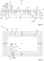
- the Figures 3A and 3B illustrate an embodiment of a chip protected against fault injection attacks.
- the figure 3A is a partial sectional and schematic view, and the figure 3B is a top view on a different scale.
- the chip 30 comprises a circuit 10 of the type of that of the figure 1 , a circuit 24 of the type of that of the figure 2 and a memory circuit 32 (MEM) formed on the front face of a semiconductor wafer 33.
- the circuits 10, 24 and 32 illustrated in FIG. figure 3A are located in a protected area 34 (IC) visible in figure 3B where these circuits are not represented.
- the chip 30 comprises an N type doped buried layer 36 situated under a P-type doped layer 37.
- the circuits 10, 24 and 32 are formed in and on the layer 37.
- the P layer 37 is in contact with the buried layer 36 on the other hand, the elements of the circuits 10, 24 and 32 do not extend to the buried layer 36.
- the periphery of the N-type buried layer 36 is in contact with an N-type doped wall 38 which extends, from the front face, into the portion of the wafer 33 located around the protected zone 34. 37, thus delimited by the buried layer 36 and the wall 38, constitutes a caisson 37.
- the wall 38 completely surrounds the protected zone 34.
- the wall 38 is surmounted by a contact 40 connected to a node 42 application of a high potential of polarization VDD.
- the contact 40 is connected to a detector 44 (DET) of the bias current I of the buried layer 36, that is to say the current absorbed by the buried layer 36 or derived therefrom.
- the detector can be located in the protected area 34.
- the portion of the wafer 33 located beneath the buried layer 36 corresponds to a p-type doped substrate 46.
- the substrate 46 is in contact with a P-type doped peripheral wall 48 that extends to the front face.
- the wall P 48 is connected to the ground GND by a contact 52 and the well P 37 is connected to the ground GND by a contact 54.
- caissons N 12 and 26 of circuits 10 and 24 can penetrate into well P 37 to a depth of less than 2 ⁇ m.
- the thickness of the caisson 37 between the lower level of the caissons N 12 and 26 and the upper level the buried layer 36 may be between 2 and 3 microns.
- the buried layer 36 may have a thickness of between 2 and 3 ⁇ m.
- the PN junctions between the buried layer 36 and the surrounding P-type doped regions 46 and 37 are polarized in reverse, and the bias current I of the buried layer 36 is negligible.
- a photogenerated current I1 flows from the buried layer 36 to the substrate P 46, and a photogenerated current I2 flows from the buried layer 36 to the chamber P 37.
- the bias current I of the buried layer 36 which comprises the two components I1 and I2, therefore increases because of the attack.
- this current I becomes greater than a threshold, the detector emits an alert signal A.
- countermeasures are taken to stop the attack, for example by destroying the confidential data or by stopping the operation of the circuits.
- Similar attacks are detected and stopped by applying a positive or negative potential by a probe on the back side of the chip.
- the detected current threshold is in absolute value of between 2 and 50 ⁇ A, for example 10 ⁇ A.
- any type of circuit formed in the upper part of the box 37 can be protected, and several circuits of different types can be protected simultaneously.
- a double-box type circuit, a triple-box type circuit and a memory circuit are protected. It is thus possible to simultaneously protect all the circuits of a chip.
- the box P 37, the wall N 38 and the wall P 48 occupy on the front face around the protected area 34 a band of small width, for example less than 4 microns.
- the surface of the chip dedicated to the protection is limited to this and at the surface of a single detector common to the circuits, while the protected area 34 may be of surface greater than 1 mm 2 .
- the surface of the chip used to protect the circuits is therefore particularly limited.
- the detection sensitivity is particularly high. Indeed, because of the presence of the P chamber 37, the bias current generated by the attack is not mixed with the circuit supply currents or the polarization currents of the boxes included in the circuits.
- the presence of the wall N 38 separated from the circuits surrounding the protected area 34 makes it possible to effectively protect the parts of the circuits situated at the periphery of the protected area.
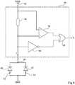
- the figure 4 illustrates an example of a detector 44 adapted to detect a current entering or leaving the buried layer 36.
- the detector 44 is connected to the application node of the potential VDD and to the contact 40 of the wall 38 connected to the buried layer 36. by a diode 60 the PN junction between the substrate 46 connected to the contact 52, and a diode 62 the PN junction between the box P 37 connected to the contact 54 and the buried layer 36.
- the detector 44 comprises a resistor 64 connecting the contact 40 to the node 42 for applying the potential VDD.
- the contact 40 is coupled by an inverter 66 to a first input of an OR gate 68.
- a comparator 70 is connected across the resistor 64, the positive input of the comparator 70 being connected to the contact 40 and the negative input being at the voltage VDD.
- the output of the comparator 70 is connected to a second input of the OR gate 68.
- the alert signal A corresponds to a high value of the output of the OR gate 68.
- the detector thus obtained contains a small number of components and is easy to implement. This detector occupies a limited area on the chip. In addition, this detector provides protection against both laser attacks and potential application attacks.
- a resistor 64 for applying the bias potential VDD to the contact 40 may be replaced by a potential application circuit VDD, this circuit providing a current I TH flowing to the contact 40 when the potential of the contact 40 is lower than the potential VDD, and opposing a resistance to the passage of current from the contact 40 when the potential of the contact 40 is greater than the potential VDD.
- the value of the current I TH then corresponds to a detection threshold of the bias current.
- the walls 38 and 48 represented in figure 3B completely surround the protected area 34, the walls 38 and 48 can be replaced by similar walls partially surrounding the protected area.
- the wall 38 may be replaced by any other means of electrically connecting the buried layer 36 to the detector 44.
- N and P conductivity types can be reversed by reversing the signs of potentials.
Landscapes
- Engineering & Computer Science (AREA)
- Computer Hardware Design (AREA)
- Theoretical Computer Science (AREA)
- Physics & Mathematics (AREA)
- Computer Security & Cryptography (AREA)
- General Engineering & Computer Science (AREA)
- Software Systems (AREA)
- General Physics & Mathematics (AREA)
- Mathematical Physics (AREA)
- Nonlinear Science (AREA)
- Microelectronics & Electronic Packaging (AREA)
- Semiconductor Integrated Circuits (AREA)
- Metal-Oxide And Bipolar Metal-Oxide Semiconductor Integrated Circuits (AREA)
- Storage Device Security (AREA)
Abstract
Description
- La présente demande concerne les puces électroniques, en particulier des puces électroniques sécurisées contre des attaques.
- Des puces électroniques telles que des puces de cartes bancaires contiennent des données confidentielles susceptibles d'être convoitées par des pirates. Pour obtenir ces informations, un pirate peut mener une attaque en balayant la face arrière de la puce par des impulsions laser. L'impact du laser perturbe le fonctionnement de la puce. C'est l'observation des conséquences de ces perturbations, parfois appelées fautes, sur l'activité du circuit, qui permet au pirate de mener à bien son attaque. Pour perturber le fonctionnement de la puce, le pirate peut aussi appliquer des potentiels positifs ou négatifs au moyen d'une sonde en contact avec la face arrière.
- Il est souhaitable de disposer de puces électroniques protégées contre ce type d'attaque, dit attaque par injection de fautes, les dispositifs connus présentant divers inconvénients et difficultés de mise en oeuvre.
- Ainsi, un mode de réalisation prévoit une puce électronique, comprenant : un substrat semiconducteur dopé d'un premier type de conductivité ; une couche enterrée dopée d'un deuxième type de conductivité recouvrant le substrat ; un premier caisson dopé du premier type de conductivité recouvrant la couche enterrée ; des circuits séparés de la couche enterrée formés dans et sur le premier caisson et/ou dans et sur des deuxièmes caissons formés dans le premier caisson ; et un détecteur du courant de polarisation de la couche enterrée.
- Selon un mode de réalisation, un premier mur du deuxième type de conductivité en contact avec la couche enterrée entoure le premier caisson.
- Selon un mode de réalisation, un deuxième mur du premier type de conductivité en contact avec le substrat entoure le premier mur.
- Selon un mode de réalisation, entre la couche enterrée et les deuxièmes caissons, le premier caisson a une épaisseur comprise entre 2 et 3 µm.
- Selon un mode de réalisation, la couche enterrée a une épaisseur comprise entre 2 et 3 µm.
- Selon un mode de réalisation, le détecteur est adapté à produire un signal d'alerte lorsque le courant de polarisation est, en valeur absolue, supérieur à une valeur comprise entre 2 et 50 µA.
- Un mode de réalisation prévoit un procédé de protection de la puce ci-dessus contre une attaque, comprenant : polariser le substrat et le premier caisson à un potentiel de référence ; polariser la couche enterrée de façon à bloquer la jonction entre la couche enterrée et le substrat et la jonction entre la couche enterrée et le premier caisson ; et produire un signal d'alerte si le courant de polarisation de la couche enterrée est supérieur à un seuil, le signal d'alerte déclenchant des contre-mesures pour stopper l'attaque.
- Ces caractéristiques et avantages, ainsi que d'autres, seront exposés en détail dans la description suivante de modes de réalisation particuliers faite à titre non limitatif en relation avec les figures jointes parmi lesquelles :
- les
figures 1 et 2 sont des vues en coupe partielles et schématiques illustrant différents types de circuit d'une puce électronique ; - la
figure 3A est une vue en coupe partielle et schématique d'un mode de réalisation d'une puce électronique protégée contre des attaques ; - la
figure 3B est une vue de dessus schématique de la puce de lafigure 3A ; et - la
figure 4 illustre un mode de réalisation d'un détecteur d'attaque. - De mêmes éléments ont été désignés par de mêmes références dans les différentes figures et, de plus, les diverses figures ne sont pas tracées à l'échelle. Par souci de clarté, seuls les éléments utiles à la compréhension des modes de réalisation décrits ont été représentés et sont détaillés. En particulier, des détails de circuits analogiques ou numériques et de circuits mémoire ne sont pas représentés.
- Dans la description qui suit, lorsque l'on fait référence à des qualificatifs de position relative, tels que les termes "dessus", "dessous", "supérieur", "inférieur", etc., il est fait référence à l'orientation de l'élément concerné dans les vues en coupe concernées.
- La
figure 1 est une vue en coupe illustrant un exemple d'un circuit 10 d'un premier type, dit à double caisson (de l'anglais "double well"), compris dans une puce électronique. Le circuit 10 comprend des transistors MOS à canal P TP et des transistors MOS à canal N TN. Les transistors TP sont formés dans et sur des caissons 12 dopés de type N situés dans la face avant d'un substrat 14 dopé de type P. Les transistors TN sont formés dans et sur des parties 16 du substrat situées entre les caissons N 12. Les caissons N 12 sont munis de contacts de polarisation 18 en face avant. Les contacts 18 sont reliés à un noeud d'application d'un potentiel haut VH. Les parties 16 sont munies de contacts de polarisation 20 en face avant reliés à une masse GND. Les transistors TP et TN sont reliés, par des conducteurs non représentés, pour former des circuits alimentés entre des potentiels haut VH1 et bas VL1. Les potentiels d'alimentation VH1 et VL1 peuvent être respectivement égaux aux potentiels de polarisation VH et GND. Les transistors TN, TP et les contacts de polarisation 18 et 20 sont séparés les uns des autres par des tranchées d'isolement 22. - La
figure 2 est une vue en coupe illustrant un exemple d'un circuit 24 d'un deuxième type, dit à triple caisson (de l'anglais "triple well") compris dans une puce électronique. Le circuit 24 reprend des éléments du circuit 10 qui ne seront pas décrits à nouveau. Dans le circuit 24, les caissons N 12 sont regroupés en un caisson profond 26 dans lequel sont formés des caissons P 16, et les contacts de polarisation 20 des caissons P 16 sont reliés à un noeud d'application d'un potentiel bas VL qui peut être différent de la masse GND. - Comme ceci a été indiqué en préambule, les circuits d'une puce peuvent contenir des informations confidentielles convoitées par un pirate. Le pirate est susceptible de chercher à obtenir ces informations par une attaque par injection de fautes. Pour cela, le pirate peut d'abord observer différents circuits de la puce à partir de la face arrière par caméra infrarouge, puis sélectionner un circuit à attaquer.
- Le pirate peut attaquer le circuit par une impulsion laser 28. Dans le cas d'un circuit de type à double caisson tel qu'illustré en
figure 1 , l'impulsion crée des paires électron-trou à proximité de la jonction PN entre un caisson N 12 et le substrat P 14. Les électrons sont séparés par le champ électrique existant à proximité de la jonction PN. Les électrons se dirigent vers les potentiels hauts du caisson N 12 et les trous se dirigent vers les potentiels bas d'une partie P 16 voisine. Il en résulte un courant IL qui s'écoule depuis le caisson N 12 vers la partie P 16. La présence d'électrons et de trous, respectivement dans le caisson 12 et dans la partie 16, perturbe le fonctionnement des transistors TN et TP. Dans le cas d'un circuit de type à triple caisson, l'impulsion laser crée un photocourant IL1 depuis le caisson N 26 vers le caisson P 16 et un photocourant IL2 depuis le caisson N 26 vers le substrat P 14, ce qui perturbe le fonctionnement des transistors. - Le pirate peut aussi attaquer le circuit en appliquant un potentiel, par exemple un potentiel positif de plusieurs dizaines de volts, au moyen d'une sonde non représentée appliquée sur la face arrière. Dans l'exemple d'un circuit de type à triple caisson, la jonction PN entre le substrat P 14 et le caisson N 26 se trouve polarisée en direct. Un transistor bipolaire constitué d'un caisson P 16, du caisson N 26 et du substrat P 14 a sa jonction base-émetteur polarisée en direct et est donc passant. De cette manière, le pirate injecte des charges dans les caissons N 26 et P 16, ce qui perturbe le fonctionnement des transistors TN et TP.
- On cherche ici à protéger contre de telles attaques des circuits du type à double caisson ou du type à triple caisson, ces circuits pouvant être des circuits numériques ou des circuits analogiques. On cherche également à protéger d'autres types de circuits, par exemple des circuits comprenant des transistors bipolaires et/ou d'autres types de composants semiconducteurs et/ou des composants tels que des capacités ou des résistances. On cherche de plus à protéger des circuits mémoire, c'est-à-dire des circuits comprenant un ensemble de points mémoire, par exemple une matrice de points mémoire.
- Les
figures 3A et 3B illustrent un mode de réalisation d'une puce 30 protégée contre des attaques par injection de fautes. Lafigure 3A est une vue en coupe partielle et schématique, et lafigure 3B est une vue de dessus à une échelle différente. - A titre d'exemple, la puce 30 comprend un circuit 10 du type de celui de la
figure 1 , un circuit 24 du type de celui de lafigure 2 et un circuit mémoire 32 (MEM) formés en face avant d'une plaquette semiconductrice 33. Les circuits 10, 24 et 32 illustrés enfigure 3A sont situés dans une zone protégée 34 (IC) visible enfigure 3B où ces circuits ne sont pas représentés. - La puce 30 comprend une couche enterrée 36 dopée de type N située sous une couche 37 dopée de type P. Les circuits 10, 24 et 32 sont formés dans et sur la couche 37. La couche P 37 est en contact avec la couche enterrée 36, par contre les éléments des circuits 10, 24 et 32 ne s'étendent pas jusqu'à la couche enterrée 36.
- La périphérie de la couche enterrée de type N 36 est en contact avec un mur 38 dopé de type N qui s'étend, à partir de la face avant, dans la partie de la plaquette 33 située autour de la zone protégée 34. La couche 37, ainsi délimitée par la couche enterrée 36 et par le mur 38, constitue un caisson 37. A titre d'exemple, le mur 38 entoure complètement la zone protégée 34. Le mur 38 est surmonté d'un contact 40 relié à un noeud 42 d'application d'un potentiel haut de polarisation VDD. Le contact 40 est relié à un détecteur 44 (DET) du courant de polarisation I de la couche enterrée 36, c'est-à-dire du courant absorbé par la couche enterrée 36 ou issu de celle-ci. Le détecteur peut être situé dans la zone protégée 34.
- La partie de la plaquette 33 située sous la couche enterrée 36 correspond à un substrat 46 dopé de type P. Le substrat 46 est en contact avec un mur périphérique 48 dopé de type P qui s'étend jusqu'à la face avant.
- Le mur P 48 est connecté à la masse GND par un contact 52 et le caisson P 37 est connecté à la masse GND par un contact 54.
- A titre d'exemple, les caissons N 12 et 26 des circuits 10 et 24 peuvent pénétrer dans le caisson P 37 jusqu'à une profondeur inférieure à 2 µm. L'épaisseur du caisson 37 entre le niveau inférieur des caissons N 12 et 26 et le niveau supérieur de la couche enterrée 36 peut être comprise entre 2 et 3 µm. La couche enterrée 36 peut avoir une épaisseur comprise entre 2 et 3 µm.
- En fonctionnement normal, c'est-à-dire en l'absence d'attaque, les jonctions PN entre la couche enterrée 36 et les régions dopées de type P 46 et 37 environnantes sont polarisées en inverse, et le courant I de polarisation de la couche enterrée 36 est négligeable.
- En cas d'attaque par un faisceau laser 28 depuis la face arrière, un courant photogénéré I1 s'écoule depuis la couche enterrée 36 vers le substrat P 46, et un courant photogénéré I2 s'écoule depuis la couche enterrée 36 vers le caisson P 37. Le courant de polarisation I de la couche enterrée 36, qui comprend les deux composantes I1 et I2, augmente donc du fait de l'attaque. Lorsque ce courant I devient supérieur à un seuil, le détecteur émet un signal d'alerte A. A la suite de la génération de ce signal d'alerte, des contre-mesures sont prises pour stopper l'attaque, par exemple en détruisant les données confidentielles ou en arrêtant le fonctionnement des circuits.
- On détecte et on stoppe de manière similaire les attaques par application d'un potentiel positif ou négatif par une sonde sur la face arrière de la puce. A titre d'exemple, le seuil de courant détecté est en valeur absolue compris entre 2 et 50 µA, par exemple 10 µA.
- Selon un avantage, du fait de la présence de la couche enterrée N 36, on peut protéger tout type de circuit formé en partie supérieure du caisson 37, et on peut protéger simultanément plusieurs circuits de types différents. Dans l'exemple représenté, un circuit du type à double caisson, un circuit du type à triple caisson et un circuit mémoire sont protégés. On peut ainsi protéger simultanément tous les circuits d'une puce.
- Selon un autre avantage, le caisson P 37, le mur N 38 et le mur P 48 occupent en face avant autour de la zone protégée 34 une bande de largeur faible, par exemple inférieure à 4 µm. La surface de la puce dédiée à la protection est limitée à cette bande et à la surface d'un seul détecteur commun aux circuits, tandis que la zone protégée 34 peut être de surface supérieure à 1 mm2. La surface de la puce utilisée pour protéger les circuits est de ce fait particulièrement limitée.
- Selon un autre avantage, la sensibilité de détection est particulièrement élevée. En effet, du fait de la présence du caisson P 37, le courant de polarisation généré par l'attaque n'est pas mêlé aux courants d'alimentation des circuits ou aux courants de polarisation des caissons compris dans les circuits.
- Selon un autre avantage, du fait de la présence de la couche enterrée de type N 36 prise en sandwich entre des régions P sous l'ensemble des circuits de la zone protégée 34, les caissons des circuits ne sont pas visibles par imagerie infrarouge. Ceci permet d'éviter que le pirate puisse choisir facilement les endroits à attaquer.
- Selon un autre avantage, la présence du mur N 38 séparé des circuits entourant la zone protégée 34 permet de protéger efficacement les parties des circuits situées en périphérie de zone protégée.
- La
figure 4 illustre un exemple de détecteur 44 adapté à détecter un courant entrant ou sortant de la couche enterrée 36. Le détecteur 44 est relié au noeud d'application du potentiel VDD et au contact 40 du mur 38 relié à la couche enterrée 36. On a représenté par une diode 60 la jonction PN entre le substrat 46 relié au contact 52, et par une diode 62 la jonction PN entre le caisson P 37 relié au contact 54 et la couche enterrée 36. - Le détecteur 44 comprend une résistance 64 reliant le contact 40 au noeud 42 d'application du potentiel VDD. Le contact 40 est couplé par un inverseur 66 à une première entrée d'une porte OU 68. Un comparateur 70 est connecté aux bornes de la résistance 64, l'entrée positive du comparateur 70 étant connectée au contact 40 et l'entrée négative étant à la tension VDD. La sortie du comparateur 70 est reliée à une deuxième entrée de la porte OU 68. Le signal d'alerte A correspond à une valeur haute de la sortie de la porte OU 68.
- En fonctionnement normal, le contact 40 est porté au potentiel VDD au travers de la résistance 64. Aucun signal d'alerte n'est émis.
- En cas d'attaque laser provoquant l'absorption par la couche enterrée d'un courant I, le potentiel du contact 40 chute et la sortie de l'inverseur 66 passe à la valeur haute, ce qui provoque l'émission du signal d'alerte A. On détecte de même une attaque par application d'un potentiel négatif élevé sur la face arrière.
- En cas d'attaque par application d'un potentiel positif sur la face arrière, un courant provenant du noeud 40 provoque une augmentation du potentiel du contact 40, et ce potentiel devient supérieur au potentiel VDD. Lorsque le potentiel du contact 40 dépasse une valeur de seuil, la sortie du comparateur 70 passe à la valeur haute, ce qui provoque l'émission du signal d'alerte A.
- Selon un avantage, le détecteur ainsi obtenu contient un nombre réduit de composants et est facile à mettre en oeuvre. Ce détecteur occupe une surface limitée sur la puce. De plus, ce détecteur permet une protection à la fois contre les attaques par laser et contre les attaques par application d'un potentiel.
- Des modes de réalisation particuliers ont été décrits. Diverses variantes et modifications apparaîtront à l'homme de l'art. En particulier, bien que l'on ait décrit, en relation avec la
figure 4 , une résistance 64 permettant d'appliquer le potentiel de polarisation VDD sur le contact 40, la résistance 64 peut être remplacée par un circuit d'application du potentiel VDD, ce circuit fournissant un courant ITH s'écoulant vers le contact 40 lorsque le potentiel du contact 40 est inférieur au potentiel VDD, et opposant une résistance au passage de courant depuis le contact 40 lorsque le potentiel du contact 40 est supérieur au potentiel VDD. La valeur du courant ITH correspond alors à un seuil de détection du courant de polarisation. - En outre, bien que les murs 38 et 48 représentés en
figure 3B entourent complètement la zone protégée 34, les murs 38 et 48 peuvent être remplacés par des murs similaires entourant partiellement la zone protégée. En outre, le mur 38 peut être remplacé par tout autre moyen de connecter électriquement la couche enterrée 36 au détecteur 44. - En outre, les types de conductivité N et P peuvent être inversés en inversant les signes des potentiels.
Claims (7)
- Puce électronique, comprenant :un substrat semiconducteur (46) dopé d'un premier type de conductivité ;une couche enterrée (36) dopée d'un deuxième type de conductivité recouvrant le substrat ;un premier caisson (37) dopé du premier type de conductivité recouvrant la couche enterrée ;des circuits (10, 24, 32) séparés de la couche enterrée formés dans et sur le premier caisson et/ou dans et sur des deuxièmes caissons (12, 26, 16) formés dans le premier caisson ; etun détecteur du courant de polarisation (I) de la couche enterrée.
- Puce selon la revendication 1, dans laquelle un premier mur (38) du deuxième type de conductivité en contact avec la couche enterrée (36) entoure le premier caisson (37).
- Puce selon la revendication 2, dans laquelle un deuxième mur (48) du premier type de conductivité en contact avec le substrat (46) entoure le premier mur (38).
- Puce selon l'une quelconque des revendications 1 à 3, dans laquelle, entre la couche enterrée et les deuxièmes caissons (12, 26), le premier caisson (37) a une épaisseur comprise entre 2 et 3 µm.
- Puce selon l'une quelconque des revendications 1 à 4, dans laquelle la couche enterrée (36) a une épaisseur comprise entre 2 et 3 µm.
- Puce selon l'une quelconque des revendications 1 à 5, dans laquelle le détecteur (44) est adapté à produire un signal d'alerte (A) lorsque le courant de polarisation (I) est, en valeur absolue, supérieur à une valeur comprise entre 2 et 50 µA.
- Procédé de protection d'une puce selon l'une quelconque des revendications 1 à 6 contre une attaque, comprenant :polariser le substrat (46) et le premier caisson (37) à un potentiel de référence (GND) ;polariser la couche enterrée (36) de façon à bloquer la jonction entre la couche enterrée et le substrat et la jonction entre la couche enterrée et le premier caisson ; etproduire un signal d'alerte (A) si le courant de polarisation (I) de la couche enterrée est supérieur à un seuil, le signal d'alerte déclenchant des contre-mesures pour stopper l'attaque.
Applications Claiming Priority (1)
| Application Number | Priority Date | Filing Date | Title |
|---|---|---|---|
| FR1659451A FR3057087B1 (fr) | 2016-09-30 | 2016-09-30 | Puce electronique protegee |
Publications (2)
| Publication Number | Publication Date |
|---|---|
| EP3301605A1 true EP3301605A1 (fr) | 2018-04-04 |
| EP3301605B1 EP3301605B1 (fr) | 2021-03-31 |
Family
ID=57960536
Family Applications (1)
| Application Number | Title | Priority Date | Filing Date |
|---|---|---|---|
| EP17156779.5A Active EP3301605B1 (fr) | 2016-09-30 | 2017-02-17 | Puce électronique protégée |
Country Status (4)
| Country | Link |
|---|---|
| US (2) | US10141396B2 (fr) |
| EP (1) | EP3301605B1 (fr) |
| CN (2) | CN206685382U (fr) |
| FR (1) | FR3057087B1 (fr) |
Cited By (2)
| Publication number | Priority date | Publication date | Assignee | Title |
|---|---|---|---|---|
| US11011479B2 (en) | 2018-07-13 | 2021-05-18 | Stmicroelectronics (Rousset) Sas | Protected electronic chip |
| US11643257B2 (en) | 2019-05-23 | 2023-05-09 | Ecolab Usa Inc. | Dispensing system |
Families Citing this family (4)
| Publication number | Priority date | Publication date | Assignee | Title |
|---|---|---|---|---|
| FR3057087B1 (fr) * | 2016-09-30 | 2018-11-16 | Stmicroelectronics (Rousset) Sas | Puce electronique protegee |
| US11082202B2 (en) * | 2018-06-01 | 2021-08-03 | Arm Limited | Fault injection attack detection in integrated circuits |
| DE102019116468B3 (de) | 2019-06-18 | 2020-10-29 | Infineon Technologies Ag | Integrierte Schaltung mit Detektionsschaltung und zugehörige Chipkarte |
| JP2024039315A (ja) * | 2022-09-09 | 2024-03-22 | キオクシア株式会社 | 半導体装置 |
Citations (4)
| Publication number | Priority date | Publication date | Assignee | Title |
|---|---|---|---|---|
| WO2004047172A1 (fr) * | 2002-11-21 | 2004-06-03 | Philips Intellectual Property & Standards Gmbh | Composant electronique de memoire dote d'une protection contre les effets nocifs de la lumiere |
| FR2958078A1 (fr) * | 2010-03-24 | 2011-09-30 | St Microelectronics Rousset | Procede et dispositif de contremesure contre une attaque par injection d'erreur dans un microcircuit electronique |
| US20130193437A1 (en) * | 2012-01-27 | 2013-08-01 | Stmicroelectronics (Rousset) Sas | Device for protecting an integrated circuit against back side attacks |
| US20130314121A1 (en) * | 2012-05-24 | 2013-11-28 | Stmicroelectronics (Grenoble 2) Sas | Method and device for protecting an integrated circuit against backside attacks |
Family Cites Families (14)
| Publication number | Priority date | Publication date | Assignee | Title |
|---|---|---|---|---|
| SE457182B (sv) * | 1987-04-03 | 1988-12-05 | Ericsson Telefon Ab L M | Anordning bestaaende av en skyddskrets foer att skydda en integrerad krets mot oeverbelastnings- och kortslutningsstroemmar |
| JP3413569B2 (ja) * | 1998-09-16 | 2003-06-03 | 株式会社日立製作所 | 絶縁ゲート型半導体装置およびその製造方法 |
| US7244992B2 (en) * | 2003-07-17 | 2007-07-17 | Ming-Dou Ker | Turn-on-efficient bipolar structures with deep N-well for on-chip ESD protection |
| US8815654B2 (en) * | 2007-06-14 | 2014-08-26 | International Business Machines Corporation | Vertical current controlled silicon on insulator (SOI) device such as a silicon controlled rectifier and method of forming vertical SOI current controlled devices |
| EP2248181B1 (fr) * | 2008-02-13 | 2014-10-22 | Acco Semiconductor, Inc | Dispositif à semi-conducteur à double grille et à tension de claquage élevée |
| US7847581B2 (en) * | 2008-04-03 | 2010-12-07 | Stmicroelectronics (Rousset) Sas | Device for protecting an integrated circuit against a laser attack |
| US8207580B2 (en) * | 2009-05-29 | 2012-06-26 | Power Integrations, Inc. | Power integrated circuit device with incorporated sense FET |
| EP2369622B1 (fr) * | 2010-03-24 | 2015-10-14 | STMicroelectronics Rousset SAS | Procédé et dispositif de contremesure contre une attaque par injection d'erreur dans un microcircuit électronique |
| FR2976721B1 (fr) * | 2011-06-17 | 2013-06-21 | St Microelectronics Rousset | Dispositif de detection d'une attaque dans une puce de circuit integre |
| FR2976722B1 (fr) * | 2011-06-17 | 2013-11-29 | St Microelectronics Rousset | Dispositif de protection d'une puce de circuit integre contre des attaques |
| FR2981783B1 (fr) * | 2011-10-19 | 2014-05-09 | St Microelectronics Rousset | Systeme de detection d'une attaque par laser d'une puce de circuit integre |
| FR2986633B1 (fr) * | 2012-02-08 | 2014-09-05 | St Microelectronics Rousset | Dispositif de detection d'une attaque par laser dans une puce de circuit integre |
| US9559066B2 (en) * | 2014-06-12 | 2017-01-31 | Broadcom Corporation | Systems and methods for detecting and preventing optical attacks |
| FR3057087B1 (fr) * | 2016-09-30 | 2018-11-16 | Stmicroelectronics (Rousset) Sas | Puce electronique protegee |
-
2016
- 2016-09-30 FR FR1659451A patent/FR3057087B1/fr not_active Expired - Fee Related
-
2017
- 2017-02-17 EP EP17156779.5A patent/EP3301605B1/fr active Active
- 2017-02-28 US US15/444,644 patent/US10141396B2/en active Active
- 2017-03-23 CN CN201720293585.XU patent/CN206685382U/zh not_active Withdrawn - After Issue
- 2017-03-23 CN CN201710179661.9A patent/CN107887337B/zh active Active
-
2018
- 2018-10-16 US US16/161,785 patent/US10388724B2/en not_active Expired - Fee Related
Patent Citations (4)
| Publication number | Priority date | Publication date | Assignee | Title |
|---|---|---|---|---|
| WO2004047172A1 (fr) * | 2002-11-21 | 2004-06-03 | Philips Intellectual Property & Standards Gmbh | Composant electronique de memoire dote d'une protection contre les effets nocifs de la lumiere |
| FR2958078A1 (fr) * | 2010-03-24 | 2011-09-30 | St Microelectronics Rousset | Procede et dispositif de contremesure contre une attaque par injection d'erreur dans un microcircuit electronique |
| US20130193437A1 (en) * | 2012-01-27 | 2013-08-01 | Stmicroelectronics (Rousset) Sas | Device for protecting an integrated circuit against back side attacks |
| US20130314121A1 (en) * | 2012-05-24 | 2013-11-28 | Stmicroelectronics (Grenoble 2) Sas | Method and device for protecting an integrated circuit against backside attacks |
Non-Patent Citations (1)
| Title |
|---|
| HAGAI BAR-EL ET AL: "The Sorcerer's Apprentice Guide to Fault Attacks", INTERNET CITATION, 7 May 2004 (2004-05-07), XP002329915, Retrieved from the Internet <URL:http://web.archive.org/web/20041016071838/eprint.iacr.org/2004/100> [retrieved on 20050527] * |
Cited By (3)
| Publication number | Priority date | Publication date | Assignee | Title |
|---|---|---|---|---|
| US11011479B2 (en) | 2018-07-13 | 2021-05-18 | Stmicroelectronics (Rousset) Sas | Protected electronic chip |
| EP3594999B1 (fr) * | 2018-07-13 | 2025-04-09 | STMicroelectronics (Rousset) SAS | Puce électronique protégée |
| US11643257B2 (en) | 2019-05-23 | 2023-05-09 | Ecolab Usa Inc. | Dispensing system |
Also Published As
| Publication number | Publication date |
|---|---|
| US20180097058A1 (en) | 2018-04-05 |
| US10388724B2 (en) | 2019-08-20 |
| US10141396B2 (en) | 2018-11-27 |
| US20190051723A1 (en) | 2019-02-14 |
| CN206685382U (zh) | 2017-11-28 |
| EP3301605B1 (fr) | 2021-03-31 |
| FR3057087B1 (fr) | 2018-11-16 |
| CN107887337A (zh) | 2018-04-06 |
| CN107887337B (zh) | 2021-02-26 |
| FR3057087A1 (fr) | 2018-04-06 |
Similar Documents
| Publication | Publication Date | Title |
|---|---|---|
| EP3301605B1 (fr) | Puce électronique protégée | |
| EP2369622B1 (fr) | Procédé et dispositif de contremesure contre une attaque par injection d'erreur dans un microcircuit électronique | |
| EP2535932B1 (fr) | Puce de circuit intégré comprenant un dispositif de protection contre des attaques | |
| EP2535933B1 (fr) | Puce de circuit intégré comprenant un dispositif de protection contre des attaques | |
| US9117833B2 (en) | Method and device for protecting an integrated circuit against backside attacks | |
| FR2981783A1 (fr) | Systeme de detection d'une attaque par laser d'une puce de circuit integre | |
| FR2812972A1 (fr) | Dispositif a semiconducteur consistant en un thyristor pour la protection contre les decharges electrostatiques | |
| FR2986633A1 (fr) | Dispositif de detection d'une attaque par laser dans une puce de circuit integre | |
| FR2986356A1 (fr) | Dispositif de protection d'un circuit integre contre des attaques en face arriere | |
| EP3159872A1 (fr) | Puce électronique sécurisée au moyen de de multiple caissons | |
| FR2993404A1 (fr) | Circuit integre sur soi comprenant un thyristor (scr) de protection contre des decharges electrostatiques | |
| EP2109139A2 (fr) | Dispositif de protection d'un circuit intégré contre une attaque par laser | |
| FR2492165A1 (fr) | Dispositif de protection contre les courants de fuite dans des circuits integres | |
| FR3005203A1 (fr) | Circuit integre sur soi comprenant un transistor de protection contre des decharges electrostatiques | |
| FR3016999A1 (fr) | Dispositif electronique, en particulier pour la protection contre les decharges electrostatiques | |
| EP3151277B1 (fr) | Circuit intégré sécurisé | |
| US11233076B2 (en) | Geiger-mode focal plane array with monolithically integrated resistors | |
| FR3039014B1 (fr) | Protection de ligne telephonique contre les surtensions | |
| FR2684240A1 (fr) | Transistor mos a zener de protection integree. | |
| EP3525236B1 (fr) | Procédé de détection d'une atteinte à l'intégrité d'un substrat semi-conducteur d'un circuit intégré depuis sa face arrière, et dispositif correspondant | |
| FR3071100A1 (fr) | Procede de detection d'un amincissement d'un substrat de circuit integre par sa face arriere, et circuit integre correspondant | |
| FR3112004A1 (fr) | Détection d'une impulsion électromagnétique | |
| EP3594999B1 (fr) | Puce électronique protégée | |
| EP3593380A1 (fr) | Puce electronique | |
| EP3373330B1 (fr) | Architecture de puce électronique |
Legal Events
| Date | Code | Title | Description |
|---|---|---|---|
| PUAI | Public reference made under article 153(3) epc to a published international application that has entered the european phase |
Free format text: ORIGINAL CODE: 0009012 |
|
| STAA | Information on the status of an ep patent application or granted ep patent |
Free format text: STATUS: REQUEST FOR EXAMINATION WAS MADE |
|
| 17P | Request for examination filed |
Effective date: 20170217 |
|
| AK | Designated contracting states |
Kind code of ref document: A1 Designated state(s): AL AT BE BG CH CY CZ DE DK EE ES FI FR GB GR HR HU IE IS IT LI LT LU LV MC MK MT NL NO PL PT RO RS SE SI SK SM TR |
|
| AX | Request for extension of the european patent |
Extension state: BA ME |
|
| STAA | Information on the status of an ep patent application or granted ep patent |
Free format text: STATUS: EXAMINATION IS IN PROGRESS |
|
| 17Q | First examination report despatched |
Effective date: 20200107 |
|
| GRAP | Despatch of communication of intention to grant a patent |
Free format text: ORIGINAL CODE: EPIDOSNIGR1 |
|
| STAA | Information on the status of an ep patent application or granted ep patent |
Free format text: STATUS: GRANT OF PATENT IS INTENDED |
|
| RIC1 | Information provided on ipc code assigned before grant |
Ipc: H03K 5/24 20060101ALI20200929BHEP Ipc: G06F 21/77 20130101ALI20200929BHEP Ipc: H01L 29/66 20060101ALN20200929BHEP Ipc: H01L 27/092 20060101ALI20200929BHEP Ipc: H01L 21/8238 20060101ALI20200929BHEP Ipc: H01L 29/10 20060101ALI20200929BHEP Ipc: G06F 21/87 20130101ALI20200929BHEP Ipc: H01L 23/00 20060101ALN20200929BHEP Ipc: G06F 21/75 20130101AFI20200929BHEP |
|
| INTG | Intention to grant announced |
Effective date: 20201013 |
|
| GRAS | Grant fee paid |
Free format text: ORIGINAL CODE: EPIDOSNIGR3 |
|
| GRAA | (expected) grant |
Free format text: ORIGINAL CODE: 0009210 |
|
| STAA | Information on the status of an ep patent application or granted ep patent |
Free format text: STATUS: THE PATENT HAS BEEN GRANTED |
|
| AK | Designated contracting states |
Kind code of ref document: B1 Designated state(s): AL AT BE BG CH CY CZ DE DK EE ES FI FR GB GR HR HU IE IS IT LI LT LU LV MC MK MT NL NO PL PT RO RS SE SI SK SM TR |
|
| REG | Reference to a national code |
Ref country code: GB Ref legal event code: FG4D Free format text: NOT ENGLISH Ref country code: CH Ref legal event code: EP |
|
| REG | Reference to a national code |
Ref country code: DE Ref legal event code: R096 Ref document number: 602017035525 Country of ref document: DE Ref country code: AT Ref legal event code: REF Ref document number: 1377751 Country of ref document: AT Kind code of ref document: T Effective date: 20210415 |
|
| REG | Reference to a national code |
Ref country code: IE Ref legal event code: FG4D Free format text: LANGUAGE OF EP DOCUMENT: FRENCH |
|
| REG | Reference to a national code |
Ref country code: LT Ref legal event code: MG9D |
|
| PG25 | Lapsed in a contracting state [announced via postgrant information from national office to epo] |
Ref country code: BG Free format text: LAPSE BECAUSE OF FAILURE TO SUBMIT A TRANSLATION OF THE DESCRIPTION OR TO PAY THE FEE WITHIN THE PRESCRIBED TIME-LIMIT Effective date: 20210630 Ref country code: FI Free format text: LAPSE BECAUSE OF FAILURE TO SUBMIT A TRANSLATION OF THE DESCRIPTION OR TO PAY THE FEE WITHIN THE PRESCRIBED TIME-LIMIT Effective date: 20210331 Ref country code: HR Free format text: LAPSE BECAUSE OF FAILURE TO SUBMIT A TRANSLATION OF THE DESCRIPTION OR TO PAY THE FEE WITHIN THE PRESCRIBED TIME-LIMIT Effective date: 20210331 Ref country code: NO Free format text: LAPSE BECAUSE OF FAILURE TO SUBMIT A TRANSLATION OF THE DESCRIPTION OR TO PAY THE FEE WITHIN THE PRESCRIBED TIME-LIMIT Effective date: 20210630 |
|
| PG25 | Lapsed in a contracting state [announced via postgrant information from national office to epo] |
Ref country code: LV Free format text: LAPSE BECAUSE OF FAILURE TO SUBMIT A TRANSLATION OF THE DESCRIPTION OR TO PAY THE FEE WITHIN THE PRESCRIBED TIME-LIMIT Effective date: 20210331 Ref country code: RS Free format text: LAPSE BECAUSE OF FAILURE TO SUBMIT A TRANSLATION OF THE DESCRIPTION OR TO PAY THE FEE WITHIN THE PRESCRIBED TIME-LIMIT Effective date: 20210331 Ref country code: SE Free format text: LAPSE BECAUSE OF FAILURE TO SUBMIT A TRANSLATION OF THE DESCRIPTION OR TO PAY THE FEE WITHIN THE PRESCRIBED TIME-LIMIT Effective date: 20210331 |
|
| REG | Reference to a national code |
Ref country code: NL Ref legal event code: MP Effective date: 20210331 |
|
| REG | Reference to a national code |
Ref country code: AT Ref legal event code: MK05 Ref document number: 1377751 Country of ref document: AT Kind code of ref document: T Effective date: 20210331 |
|
| PG25 | Lapsed in a contracting state [announced via postgrant information from national office to epo] |
Ref country code: CZ Free format text: LAPSE BECAUSE OF FAILURE TO SUBMIT A TRANSLATION OF THE DESCRIPTION OR TO PAY THE FEE WITHIN THE PRESCRIBED TIME-LIMIT Effective date: 20210331 Ref country code: EE Free format text: LAPSE BECAUSE OF FAILURE TO SUBMIT A TRANSLATION OF THE DESCRIPTION OR TO PAY THE FEE WITHIN THE PRESCRIBED TIME-LIMIT Effective date: 20210331 Ref country code: LT Free format text: LAPSE BECAUSE OF FAILURE TO SUBMIT A TRANSLATION OF THE DESCRIPTION OR TO PAY THE FEE WITHIN THE PRESCRIBED TIME-LIMIT Effective date: 20210331 Ref country code: NL Free format text: LAPSE BECAUSE OF FAILURE TO SUBMIT A TRANSLATION OF THE DESCRIPTION OR TO PAY THE FEE WITHIN THE PRESCRIBED TIME-LIMIT Effective date: 20210331 Ref country code: SM Free format text: LAPSE BECAUSE OF FAILURE TO SUBMIT A TRANSLATION OF THE DESCRIPTION OR TO PAY THE FEE WITHIN THE PRESCRIBED TIME-LIMIT Effective date: 20210331 Ref country code: AT Free format text: LAPSE BECAUSE OF FAILURE TO SUBMIT A TRANSLATION OF THE DESCRIPTION OR TO PAY THE FEE WITHIN THE PRESCRIBED TIME-LIMIT Effective date: 20210331 |
|
| PG25 | Lapsed in a contracting state [announced via postgrant information from national office to epo] |
Ref country code: IS Free format text: LAPSE BECAUSE OF FAILURE TO SUBMIT A TRANSLATION OF THE DESCRIPTION OR TO PAY THE FEE WITHIN THE PRESCRIBED TIME-LIMIT Effective date: 20210731 Ref country code: PL Free format text: LAPSE BECAUSE OF FAILURE TO SUBMIT A TRANSLATION OF THE DESCRIPTION OR TO PAY THE FEE WITHIN THE PRESCRIBED TIME-LIMIT Effective date: 20210331 Ref country code: PT Free format text: LAPSE BECAUSE OF FAILURE TO SUBMIT A TRANSLATION OF THE DESCRIPTION OR TO PAY THE FEE WITHIN THE PRESCRIBED TIME-LIMIT Effective date: 20210802 Ref country code: RO Free format text: LAPSE BECAUSE OF FAILURE TO SUBMIT A TRANSLATION OF THE DESCRIPTION OR TO PAY THE FEE WITHIN THE PRESCRIBED TIME-LIMIT Effective date: 20210331 Ref country code: SK Free format text: LAPSE BECAUSE OF FAILURE TO SUBMIT A TRANSLATION OF THE DESCRIPTION OR TO PAY THE FEE WITHIN THE PRESCRIBED TIME-LIMIT Effective date: 20210331 |
|
| REG | Reference to a national code |
Ref country code: DE Ref legal event code: R097 Ref document number: 602017035525 Country of ref document: DE |
|
| PG25 | Lapsed in a contracting state [announced via postgrant information from national office to epo] |
Ref country code: AL Free format text: LAPSE BECAUSE OF FAILURE TO SUBMIT A TRANSLATION OF THE DESCRIPTION OR TO PAY THE FEE WITHIN THE PRESCRIBED TIME-LIMIT Effective date: 20210331 Ref country code: DK Free format text: LAPSE BECAUSE OF FAILURE TO SUBMIT A TRANSLATION OF THE DESCRIPTION OR TO PAY THE FEE WITHIN THE PRESCRIBED TIME-LIMIT Effective date: 20210331 Ref country code: ES Free format text: LAPSE BECAUSE OF FAILURE TO SUBMIT A TRANSLATION OF THE DESCRIPTION OR TO PAY THE FEE WITHIN THE PRESCRIBED TIME-LIMIT Effective date: 20210331 |
|
| PLBE | No opposition filed within time limit |
Free format text: ORIGINAL CODE: 0009261 |
|
| STAA | Information on the status of an ep patent application or granted ep patent |
Free format text: STATUS: NO OPPOSITION FILED WITHIN TIME LIMIT |
|
| 26N | No opposition filed |
Effective date: 20220104 |
|
| PG25 | Lapsed in a contracting state [announced via postgrant information from national office to epo] |
Ref country code: IS Free format text: LAPSE BECAUSE OF FAILURE TO SUBMIT A TRANSLATION OF THE DESCRIPTION OR TO PAY THE FEE WITHIN THE PRESCRIBED TIME-LIMIT Effective date: 20210731 |
|
| PG25 | Lapsed in a contracting state [announced via postgrant information from national office to epo] |
Ref country code: IT Free format text: LAPSE BECAUSE OF FAILURE TO SUBMIT A TRANSLATION OF THE DESCRIPTION OR TO PAY THE FEE WITHIN THE PRESCRIBED TIME-LIMIT Effective date: 20210331 |
|
| PG25 | Lapsed in a contracting state [announced via postgrant information from national office to epo] |
Ref country code: MC Free format text: LAPSE BECAUSE OF FAILURE TO SUBMIT A TRANSLATION OF THE DESCRIPTION OR TO PAY THE FEE WITHIN THE PRESCRIBED TIME-LIMIT Effective date: 20210331 |
|
| REG | Reference to a national code |
Ref country code: CH Ref legal event code: PL |
|
| REG | Reference to a national code |
Ref country code: BE Ref legal event code: MM Effective date: 20220228 |
|
| GBPC | Gb: european patent ceased through non-payment of renewal fee |
Effective date: 20220217 |
|
| PG25 | Lapsed in a contracting state [announced via postgrant information from national office to epo] |
Ref country code: LU Free format text: LAPSE BECAUSE OF NON-PAYMENT OF DUE FEES Effective date: 20220217 |
|
| PG25 | Lapsed in a contracting state [announced via postgrant information from national office to epo] |
Ref country code: FR Free format text: LAPSE BECAUSE OF NON-PAYMENT OF DUE FEES Effective date: 20220228 |
|
| PG25 | Lapsed in a contracting state [announced via postgrant information from national office to epo] |
Ref country code: LI Free format text: LAPSE BECAUSE OF NON-PAYMENT OF DUE FEES Effective date: 20220228 Ref country code: IE Free format text: LAPSE BECAUSE OF NON-PAYMENT OF DUE FEES Effective date: 20220217 Ref country code: GB Free format text: LAPSE BECAUSE OF NON-PAYMENT OF DUE FEES Effective date: 20220217 Ref country code: CH Free format text: LAPSE BECAUSE OF NON-PAYMENT OF DUE FEES Effective date: 20220228 |
|
| PG25 | Lapsed in a contracting state [announced via postgrant information from national office to epo] |
Ref country code: BE Free format text: LAPSE BECAUSE OF NON-PAYMENT OF DUE FEES Effective date: 20220228 |
|
| PG25 | Lapsed in a contracting state [announced via postgrant information from national office to epo] |
Ref country code: HU Free format text: LAPSE BECAUSE OF FAILURE TO SUBMIT A TRANSLATION OF THE DESCRIPTION OR TO PAY THE FEE WITHIN THE PRESCRIBED TIME-LIMIT; INVALID AB INITIO Effective date: 20170217 |
|
| PG25 | Lapsed in a contracting state [announced via postgrant information from national office to epo] |
Ref country code: MK Free format text: LAPSE BECAUSE OF FAILURE TO SUBMIT A TRANSLATION OF THE DESCRIPTION OR TO PAY THE FEE WITHIN THE PRESCRIBED TIME-LIMIT Effective date: 20210331 Ref country code: CY Free format text: LAPSE BECAUSE OF FAILURE TO SUBMIT A TRANSLATION OF THE DESCRIPTION OR TO PAY THE FEE WITHIN THE PRESCRIBED TIME-LIMIT Effective date: 20210331 |
|
| PG25 | Lapsed in a contracting state [announced via postgrant information from national office to epo] |
Ref country code: MT Free format text: LAPSE BECAUSE OF FAILURE TO SUBMIT A TRANSLATION OF THE DESCRIPTION OR TO PAY THE FEE WITHIN THE PRESCRIBED TIME-LIMIT Effective date: 20210331 |
|
| PG25 | Lapsed in a contracting state [announced via postgrant information from national office to epo] |
Ref country code: GR Free format text: LAPSE BECAUSE OF NON-PAYMENT OF DUE FEES Effective date: 20210331 |
|
| PG25 | Lapsed in a contracting state [announced via postgrant information from national office to epo] |
Ref country code: GR Free format text: LAPSE BECAUSE OF NON-PAYMENT OF DUE FEES Effective date: 20210331 |
|
| PG25 | Lapsed in a contracting state [announced via postgrant information from national office to epo] |
Ref country code: TR Free format text: LAPSE BECAUSE OF FAILURE TO SUBMIT A TRANSLATION OF THE DESCRIPTION OR TO PAY THE FEE WITHIN THE PRESCRIBED TIME-LIMIT Effective date: 20210331 |
|
| PGFP | Annual fee paid to national office [announced via postgrant information from national office to epo] |
Ref country code: DE Payment date: 20260121 Year of fee payment: 10 |