EP3300105B1 - Leistungshalbleitermodul und verfahren zur herstellung eines leistungshalbleitermoduls - Google Patents
Leistungshalbleitermodul und verfahren zur herstellung eines leistungshalbleitermoduls Download PDFInfo
- Publication number
- EP3300105B1 EP3300105B1 EP16190518.7A EP16190518A EP3300105B1 EP 3300105 B1 EP3300105 B1 EP 3300105B1 EP 16190518 A EP16190518 A EP 16190518A EP 3300105 B1 EP3300105 B1 EP 3300105B1
- Authority
- EP
- European Patent Office
- Prior art keywords
- metal plate
- semiconductor chip
- substrate
- opening
- electrically conductive
- Prior art date
- Legal status (The legal status is an assumption and is not a legal conclusion. Google has not performed a legal analysis and makes no representation as to the accuracy of the status listed.)
- Active
Links
- 239000004065 semiconductor Substances 0.000 title claims description 247
- 238000000034 method Methods 0.000 title claims description 55
- 238000004519 manufacturing process Methods 0.000 title claims description 26
- 229910052751 metal Inorganic materials 0.000 claims description 250
- 239000002184 metal Substances 0.000 claims description 250
- 239000000758 substrate Substances 0.000 claims description 157
- 150000001875 compounds Chemical class 0.000 claims description 65
- 238000001465 metallisation Methods 0.000 claims description 43
- 239000000463 material Substances 0.000 claims description 32
- 238000005530 etching Methods 0.000 claims description 24
- 230000000712 assembly Effects 0.000 claims description 14
- 238000000429 assembly Methods 0.000 claims description 14
- 239000007787 solid Substances 0.000 claims description 11
- 238000000151 deposition Methods 0.000 claims description 6
- 239000002243 precursor Substances 0.000 claims description 3
- 238000002955 isolation Methods 0.000 claims 2
- 239000000470 constituent Substances 0.000 claims 1
- 239000012530 fluid Substances 0.000 claims 1
- 239000010410 layer Substances 0.000 description 193
- RYGMFSIKBFXOCR-UHFFFAOYSA-N Copper Chemical group [Cu] RYGMFSIKBFXOCR-UHFFFAOYSA-N 0.000 description 22
- 239000002131 composite material Substances 0.000 description 21
- 239000010949 copper Substances 0.000 description 21
- 239000011347 resin Substances 0.000 description 19
- 229920005989 resin Polymers 0.000 description 19
- 229910052802 copper Inorganic materials 0.000 description 18
- 239000012790 adhesive layer Substances 0.000 description 15
- 239000000945 filler Substances 0.000 description 15
- 238000009413 insulation Methods 0.000 description 15
- 230000008569 process Effects 0.000 description 14
- 239000000843 powder Substances 0.000 description 13
- 239000000919 ceramic Substances 0.000 description 12
- 238000004873 anchoring Methods 0.000 description 10
- 239000004033 plastic Substances 0.000 description 10
- 229920003023 plastic Polymers 0.000 description 10
- PXHVJJICTQNCMI-UHFFFAOYSA-N Nickel Chemical compound [Ni] PXHVJJICTQNCMI-UHFFFAOYSA-N 0.000 description 9
- 239000004020 conductor Substances 0.000 description 9
- 229910000679 solder Inorganic materials 0.000 description 9
- 238000005137 deposition process Methods 0.000 description 8
- 238000005245 sintering Methods 0.000 description 8
- 239000000203 mixture Substances 0.000 description 7
- 229910052581 Si3N4 Inorganic materials 0.000 description 6
- 229910052782 aluminium Inorganic materials 0.000 description 6
- XAGFODPZIPBFFR-UHFFFAOYSA-N aluminium Chemical compound [Al] XAGFODPZIPBFFR-UHFFFAOYSA-N 0.000 description 6
- 230000009969 flowable effect Effects 0.000 description 6
- 150000002739 metals Chemical class 0.000 description 6
- HQVNEWCFYHHQES-UHFFFAOYSA-N silicon nitride Chemical compound N12[Si]34N5[Si]62N3[Si]51N64 HQVNEWCFYHHQES-UHFFFAOYSA-N 0.000 description 6
- ZOKXTWBITQBERF-UHFFFAOYSA-N Molybdenum Chemical compound [Mo] ZOKXTWBITQBERF-UHFFFAOYSA-N 0.000 description 5
- VYPSYNLAJGMNEJ-UHFFFAOYSA-N Silicium dioxide Chemical compound O=[Si]=O VYPSYNLAJGMNEJ-UHFFFAOYSA-N 0.000 description 5
- 229910045601 alloy Inorganic materials 0.000 description 5
- 239000000956 alloy Substances 0.000 description 5
- 239000011889 copper foil Substances 0.000 description 5
- TWNQGVIAIRXVLR-UHFFFAOYSA-N oxo(oxoalumanyloxy)alumane Chemical compound O=[Al]O[Al]=O TWNQGVIAIRXVLR-UHFFFAOYSA-N 0.000 description 5
- 239000002245 particle Substances 0.000 description 5
- 239000002904 solvent Substances 0.000 description 5
- 239000007858 starting material Substances 0.000 description 5
- BQCADISMDOOEFD-UHFFFAOYSA-N Silver Chemical compound [Ag] BQCADISMDOOEFD-UHFFFAOYSA-N 0.000 description 4
- 238000001816 cooling Methods 0.000 description 4
- 239000011888 foil Substances 0.000 description 4
- 239000010931 gold Substances 0.000 description 4
- 229910052750 molybdenum Inorganic materials 0.000 description 4
- 239000011733 molybdenum Substances 0.000 description 4
- 238000005498 polishing Methods 0.000 description 4
- 229910052709 silver Inorganic materials 0.000 description 4
- 239000004332 silver Substances 0.000 description 4
- XUIMIQQOPSSXEZ-UHFFFAOYSA-N Silicon Chemical compound [Si] XUIMIQQOPSSXEZ-UHFFFAOYSA-N 0.000 description 3
- 238000005234 chemical deposition Methods 0.000 description 3
- 230000008021 deposition Effects 0.000 description 3
- 239000003989 dielectric material Substances 0.000 description 3
- 239000006260 foam Substances 0.000 description 3
- 238000000227 grinding Methods 0.000 description 3
- 229910052759 nickel Inorganic materials 0.000 description 3
- BASFCYQUMIYNBI-UHFFFAOYSA-N platinum Chemical compound [Pt] BASFCYQUMIYNBI-UHFFFAOYSA-N 0.000 description 3
- 229910052710 silicon Inorganic materials 0.000 description 3
- 239000010703 silicon Substances 0.000 description 3
- 239000010936 titanium Substances 0.000 description 3
- 229910018072 Al 2 O 3 Inorganic materials 0.000 description 2
- 229910000838 Al alloy Inorganic materials 0.000 description 2
- PIGFYZPCRLYGLF-UHFFFAOYSA-N Aluminum nitride Chemical compound [Al]#N PIGFYZPCRLYGLF-UHFFFAOYSA-N 0.000 description 2
- 229910052582 BN Inorganic materials 0.000 description 2
- PZNSFCLAULLKQX-UHFFFAOYSA-N Boron nitride Chemical compound N#B PZNSFCLAULLKQX-UHFFFAOYSA-N 0.000 description 2
- 229910000881 Cu alloy Inorganic materials 0.000 description 2
- ATJFFYVFTNAWJD-UHFFFAOYSA-N Tin Chemical compound [Sn] ATJFFYVFTNAWJD-UHFFFAOYSA-N 0.000 description 2
- RTAQQCXQSZGOHL-UHFFFAOYSA-N Titanium Chemical compound [Ti] RTAQQCXQSZGOHL-UHFFFAOYSA-N 0.000 description 2
- 239000000853 adhesive Substances 0.000 description 2
- 230000001070 adhesive effect Effects 0.000 description 2
- -1 alloys Chemical class 0.000 description 2
- 230000000903 blocking effect Effects 0.000 description 2
- 239000011248 coating agent Substances 0.000 description 2
- 238000000576 coating method Methods 0.000 description 2
- PMHQVHHXPFUNSP-UHFFFAOYSA-M copper(1+);methylsulfanylmethane;bromide Chemical compound Br[Cu].CSC PMHQVHHXPFUNSP-UHFFFAOYSA-M 0.000 description 2
- 239000010432 diamond Substances 0.000 description 2
- 229910003460 diamond Inorganic materials 0.000 description 2
- 230000008020 evaporation Effects 0.000 description 2
- 238000001704 evaporation Methods 0.000 description 2
- 230000005669 field effect Effects 0.000 description 2
- 239000011521 glass Substances 0.000 description 2
- PCHJSUWPFVWCPO-UHFFFAOYSA-N gold Chemical compound [Au] PCHJSUWPFVWCPO-UHFFFAOYSA-N 0.000 description 2
- 229910052737 gold Inorganic materials 0.000 description 2
- 238000002347 injection Methods 0.000 description 2
- 239000007924 injection Substances 0.000 description 2
- 238000001746 injection moulding Methods 0.000 description 2
- 239000007788 liquid Substances 0.000 description 2
- 239000002905 metal composite material Substances 0.000 description 2
- 229910001092 metal group alloy Inorganic materials 0.000 description 2
- 238000005289 physical deposition Methods 0.000 description 2
- 238000005240 physical vapour deposition Methods 0.000 description 2
- 238000001020 plasma etching Methods 0.000 description 2
- 239000004848 polyfunctional curative Substances 0.000 description 2
- 238000001272 pressureless sintering Methods 0.000 description 2
- HBMJWWWQQXIZIP-UHFFFAOYSA-N silicon carbide Chemical compound [Si+]#[C-] HBMJWWWQQXIZIP-UHFFFAOYSA-N 0.000 description 2
- 229910010271 silicon carbide Inorganic materials 0.000 description 2
- 235000012239 silicon dioxide Nutrition 0.000 description 2
- 239000000377 silicon dioxide Substances 0.000 description 2
- 229910052719 titanium Inorganic materials 0.000 description 2
- PFNQVRZLDWYSCW-UHFFFAOYSA-N (fluoren-9-ylideneamino) n-naphthalen-1-ylcarbamate Chemical compound C12=CC=CC=C2C2=CC=CC=C2C1=NOC(=O)NC1=CC=CC2=CC=CC=C12 PFNQVRZLDWYSCW-UHFFFAOYSA-N 0.000 description 1
- WUPHOULIZUERAE-UHFFFAOYSA-N 3-(oxolan-2-yl)propanoic acid Chemical compound OC(=O)CCC1CCCO1 WUPHOULIZUERAE-UHFFFAOYSA-N 0.000 description 1
- JBRZTFJDHDCESZ-UHFFFAOYSA-N AsGa Chemical compound [As]#[Ga] JBRZTFJDHDCESZ-UHFFFAOYSA-N 0.000 description 1
- 229910002601 GaN Inorganic materials 0.000 description 1
- 229910005540 GaP Inorganic materials 0.000 description 1
- 229910001218 Gallium arsenide Inorganic materials 0.000 description 1
- JMASRVWKEDWRBT-UHFFFAOYSA-N Gallium nitride Chemical compound [Ga]#N JMASRVWKEDWRBT-UHFFFAOYSA-N 0.000 description 1
- GPXJNWSHGFTCBW-UHFFFAOYSA-N Indium phosphide Chemical compound [In]#P GPXJNWSHGFTCBW-UHFFFAOYSA-N 0.000 description 1
- 229910000577 Silicon-germanium Inorganic materials 0.000 description 1
- LEVVHYCKPQWKOP-UHFFFAOYSA-N [Si].[Ge] Chemical compound [Si].[Ge] LEVVHYCKPQWKOP-UHFFFAOYSA-N 0.000 description 1
- SMNRFWMNPDABKZ-WVALLCKVSA-N [[(2R,3S,4R,5S)-5-(2,6-dioxo-3H-pyridin-3-yl)-3,4-dihydroxyoxolan-2-yl]methoxy-hydroxyphosphoryl] [[[(2R,3S,4S,5R,6R)-4-fluoro-3,5-dihydroxy-6-(hydroxymethyl)oxan-2-yl]oxy-hydroxyphosphoryl]oxy-hydroxyphosphoryl] hydrogen phosphate Chemical compound OC[C@H]1O[C@H](OP(O)(=O)OP(O)(=O)OP(O)(=O)OP(O)(=O)OC[C@H]2O[C@H]([C@H](O)[C@@H]2O)C2C=CC(=O)NC2=O)[C@H](O)[C@@H](F)[C@@H]1O SMNRFWMNPDABKZ-WVALLCKVSA-N 0.000 description 1
- 238000010521 absorption reaction Methods 0.000 description 1
- 230000009471 action Effects 0.000 description 1
- 239000002318 adhesion promoter Substances 0.000 description 1
- OPIARDKIWVCIRZ-UHFFFAOYSA-N aluminum;copper Chemical compound [Al+3].[Cu+2] OPIARDKIWVCIRZ-UHFFFAOYSA-N 0.000 description 1
- 238000000149 argon plasma sintering Methods 0.000 description 1
- 229910052980 cadmium sulfide Inorganic materials 0.000 description 1
- 238000005266 casting Methods 0.000 description 1
- 230000008859 change Effects 0.000 description 1
- 238000005229 chemical vapour deposition Methods 0.000 description 1
- 210000000078 claw Anatomy 0.000 description 1
- 238000000748 compression moulding Methods 0.000 description 1
- 238000011161 development Methods 0.000 description 1
- 230000018109 developmental process Effects 0.000 description 1
- 239000012777 electrically insulating material Substances 0.000 description 1
- 238000009713 electroplating Methods 0.000 description 1
- 238000004049 embossing Methods 0.000 description 1
- HZXMRANICFIONG-UHFFFAOYSA-N gallium phosphide Chemical compound [Ga]#P HZXMRANICFIONG-UHFFFAOYSA-N 0.000 description 1
- 229910052732 germanium Inorganic materials 0.000 description 1
- GNPVGFCGXDBREM-UHFFFAOYSA-N germanium atom Chemical compound [Ge] GNPVGFCGXDBREM-UHFFFAOYSA-N 0.000 description 1
- 229920006015 heat resistant resin Polymers 0.000 description 1
- 238000001513 hot isostatic pressing Methods 0.000 description 1
- 238000003384 imaging method Methods 0.000 description 1
- 150000003949 imides Chemical class 0.000 description 1
- 238000007373 indentation Methods 0.000 description 1
- WPYVAWXEWQSOGY-UHFFFAOYSA-N indium antimonide Chemical compound [Sb]#[In] WPYVAWXEWQSOGY-UHFFFAOYSA-N 0.000 description 1
- 229910044991 metal oxide Inorganic materials 0.000 description 1
- 150000004706 metal oxides Chemical class 0.000 description 1
- 239000002923 metal particle Substances 0.000 description 1
- 238000003801 milling Methods 0.000 description 1
- 150000004767 nitrides Chemical class 0.000 description 1
- 238000013021 overheating Methods 0.000 description 1
- 238000002161 passivation Methods 0.000 description 1
- 229910052697 platinum Inorganic materials 0.000 description 1
- 229910021420 polycrystalline silicon Inorganic materials 0.000 description 1
- 238000000926 separation method Methods 0.000 description 1
- 230000035939 shock Effects 0.000 description 1
- 229910021332 silicide Inorganic materials 0.000 description 1
- FVBUAEGBCNSCDD-UHFFFAOYSA-N silicide(4-) Chemical compound [Si-4] FVBUAEGBCNSCDD-UHFFFAOYSA-N 0.000 description 1
- 229910052814 silicon oxide Inorganic materials 0.000 description 1
- 238000007711 solidification Methods 0.000 description 1
- 230000008023 solidification Effects 0.000 description 1
- 238000003892 spreading Methods 0.000 description 1
- 230000007480 spreading Effects 0.000 description 1
- 238000004544 sputter deposition Methods 0.000 description 1
- 239000000126 substance Substances 0.000 description 1
- 229910052715 tantalum Inorganic materials 0.000 description 1
- GUVRBAGPIYLISA-UHFFFAOYSA-N tantalum atom Chemical compound [Ta] GUVRBAGPIYLISA-UHFFFAOYSA-N 0.000 description 1
- 229920001169 thermoplastic Polymers 0.000 description 1
- 239000004416 thermosoftening plastic Substances 0.000 description 1
- MAKDTFFYCIMFQP-UHFFFAOYSA-N titanium tungsten Chemical compound [Ti].[W] MAKDTFFYCIMFQP-UHFFFAOYSA-N 0.000 description 1
- 238000001721 transfer moulding Methods 0.000 description 1
- WFKWXMTUELFFGS-UHFFFAOYSA-N tungsten Chemical compound [W] WFKWXMTUELFFGS-UHFFFAOYSA-N 0.000 description 1
- 229910052721 tungsten Inorganic materials 0.000 description 1
- 239000010937 tungsten Substances 0.000 description 1
- 238000007740 vapor deposition Methods 0.000 description 1
- 238000003466 welding Methods 0.000 description 1
Images


Classifications
-
- H—ELECTRICITY
- H01—ELECTRIC ELEMENTS
- H01L—SEMICONDUCTOR DEVICES NOT COVERED BY CLASS H10
- H01L24/00—Arrangements for connecting or disconnecting semiconductor or solid-state bodies; Methods or apparatus related thereto
- H01L24/93—Batch processes
- H01L24/95—Batch processes at chip-level, i.e. with connecting carried out on a plurality of singulated devices, i.e. on diced chips
- H01L24/97—Batch processes at chip-level, i.e. with connecting carried out on a plurality of singulated devices, i.e. on diced chips the devices being connected to a common substrate, e.g. interposer, said common substrate being separable into individual assemblies after connecting
-
- H—ELECTRICITY
- H01—ELECTRIC ELEMENTS
- H01L—SEMICONDUCTOR DEVICES NOT COVERED BY CLASS H10
- H01L21/00—Processes or apparatus adapted for the manufacture or treatment of semiconductor or solid state devices or of parts thereof
- H01L21/02—Manufacture or treatment of semiconductor devices or of parts thereof
- H01L21/04—Manufacture or treatment of semiconductor devices or of parts thereof the devices having at least one potential-jump barrier or surface barrier, e.g. PN junction, depletion layer or carrier concentration layer
- H01L21/48—Manufacture or treatment of parts, e.g. containers, prior to assembly of the devices, using processes not provided for in a single one of the subgroups H01L21/06 - H01L21/326
- H01L21/4814—Conductive parts
- H01L21/4846—Leads on or in insulating or insulated substrates, e.g. metallisation
- H01L21/4853—Connection or disconnection of other leads to or from a metallisation, e.g. pins, wires, bumps
-
- H—ELECTRICITY
- H01—ELECTRIC ELEMENTS
- H01L—SEMICONDUCTOR DEVICES NOT COVERED BY CLASS H10
- H01L23/00—Details of semiconductor or other solid state devices
- H01L23/48—Arrangements for conducting electric current to or from the solid state body in operation, e.g. leads, terminal arrangements ; Selection of materials therefor
- H01L23/488—Arrangements for conducting electric current to or from the solid state body in operation, e.g. leads, terminal arrangements ; Selection of materials therefor consisting of soldered or bonded constructions
- H01L23/498—Leads, i.e. metallisations or lead-frames on insulating substrates, e.g. chip carriers
- H01L23/49811—Additional leads joined to the metallisation on the insulating substrate, e.g. pins, bumps, wires, flat leads
-
- H—ELECTRICITY
- H01—ELECTRIC ELEMENTS
- H01L—SEMICONDUCTOR DEVICES NOT COVERED BY CLASS H10
- H01L23/00—Details of semiconductor or other solid state devices
- H01L23/52—Arrangements for conducting electric current within the device in operation from one component to another, i.e. interconnections, e.g. wires, lead frames
- H01L23/538—Arrangements for conducting electric current within the device in operation from one component to another, i.e. interconnections, e.g. wires, lead frames the interconnection structure between a plurality of semiconductor chips being formed on, or in, insulating substrates
- H01L23/5389—Arrangements for conducting electric current within the device in operation from one component to another, i.e. interconnections, e.g. wires, lead frames the interconnection structure between a plurality of semiconductor chips being formed on, or in, insulating substrates the chips being integrally enclosed by the interconnect and support structures
-
- H—ELECTRICITY
- H01—ELECTRIC ELEMENTS
- H01L—SEMICONDUCTOR DEVICES NOT COVERED BY CLASS H10
- H01L23/00—Details of semiconductor or other solid state devices
- H01L23/544—Marks applied to semiconductor devices or parts, e.g. registration marks, alignment structures, wafer maps
-
- H—ELECTRICITY
- H01—ELECTRIC ELEMENTS
- H01L—SEMICONDUCTOR DEVICES NOT COVERED BY CLASS H10
- H01L24/00—Arrangements for connecting or disconnecting semiconductor or solid-state bodies; Methods or apparatus related thereto
- H01L24/01—Means for bonding being attached to, or being formed on, the surface to be connected, e.g. chip-to-package, die-attach, "first-level" interconnects; Manufacturing methods related thereto
- H01L24/18—High density interconnect [HDI] connectors; Manufacturing methods related thereto
- H01L24/23—Structure, shape, material or disposition of the high density interconnect connectors after the connecting process
- H01L24/24—Structure, shape, material or disposition of the high density interconnect connectors after the connecting process of an individual high density interconnect connector
-
- H—ELECTRICITY
- H01—ELECTRIC ELEMENTS
- H01L—SEMICONDUCTOR DEVICES NOT COVERED BY CLASS H10
- H01L24/00—Arrangements for connecting or disconnecting semiconductor or solid-state bodies; Methods or apparatus related thereto
- H01L24/80—Methods for connecting semiconductor or other solid state bodies using means for bonding being attached to, or being formed on, the surface to be connected
- H01L24/82—Methods for connecting semiconductor or other solid state bodies using means for bonding being attached to, or being formed on, the surface to be connected by forming build-up interconnects at chip-level, e.g. for high density interconnects [HDI]
-
- H—ELECTRICITY
- H01—ELECTRIC ELEMENTS
- H01L—SEMICONDUCTOR DEVICES NOT COVERED BY CLASS H10
- H01L24/00—Arrangements for connecting or disconnecting semiconductor or solid-state bodies; Methods or apparatus related thereto
- H01L24/91—Methods for connecting semiconductor or solid state bodies including different methods provided for in two or more of groups H01L24/80 - H01L24/90
- H01L24/92—Specific sequence of method steps
-
- H—ELECTRICITY
- H01—ELECTRIC ELEMENTS
- H01L—SEMICONDUCTOR DEVICES NOT COVERED BY CLASS H10
- H01L25/00—Assemblies consisting of a plurality of individual semiconductor or other solid state devices ; Multistep manufacturing processes thereof
- H01L25/03—Assemblies consisting of a plurality of individual semiconductor or other solid state devices ; Multistep manufacturing processes thereof all the devices being of a type provided for in the same subgroup of groups H01L27/00 - H01L33/00, or in a single subclass of H10K, H10N, e.g. assemblies of rectifier diodes
- H01L25/04—Assemblies consisting of a plurality of individual semiconductor or other solid state devices ; Multistep manufacturing processes thereof all the devices being of a type provided for in the same subgroup of groups H01L27/00 - H01L33/00, or in a single subclass of H10K, H10N, e.g. assemblies of rectifier diodes the devices not having separate containers
- H01L25/07—Assemblies consisting of a plurality of individual semiconductor or other solid state devices ; Multistep manufacturing processes thereof all the devices being of a type provided for in the same subgroup of groups H01L27/00 - H01L33/00, or in a single subclass of H10K, H10N, e.g. assemblies of rectifier diodes the devices not having separate containers the devices being of a type provided for in group H01L29/00
- H01L25/072—Assemblies consisting of a plurality of individual semiconductor or other solid state devices ; Multistep manufacturing processes thereof all the devices being of a type provided for in the same subgroup of groups H01L27/00 - H01L33/00, or in a single subclass of H10K, H10N, e.g. assemblies of rectifier diodes the devices not having separate containers the devices being of a type provided for in group H01L29/00 the devices being arranged next to each other
-
- H—ELECTRICITY
- H01—ELECTRIC ELEMENTS
- H01L—SEMICONDUCTOR DEVICES NOT COVERED BY CLASS H10
- H01L25/00—Assemblies consisting of a plurality of individual semiconductor or other solid state devices ; Multistep manufacturing processes thereof
- H01L25/18—Assemblies consisting of a plurality of individual semiconductor or other solid state devices ; Multistep manufacturing processes thereof the devices being of types provided for in two or more different subgroups of the same main group of groups H01L27/00 - H01L33/00, or in a single subclass of H10K, H10N
-
- H—ELECTRICITY
- H01—ELECTRIC ELEMENTS
- H01L—SEMICONDUCTOR DEVICES NOT COVERED BY CLASS H10
- H01L21/00—Processes or apparatus adapted for the manufacture or treatment of semiconductor or solid state devices or of parts thereof
- H01L21/02—Manufacture or treatment of semiconductor devices or of parts thereof
- H01L21/04—Manufacture or treatment of semiconductor devices or of parts thereof the devices having at least one potential-jump barrier or surface barrier, e.g. PN junction, depletion layer or carrier concentration layer
- H01L21/48—Manufacture or treatment of parts, e.g. containers, prior to assembly of the devices, using processes not provided for in a single one of the subgroups H01L21/06 - H01L21/326
- H01L21/4814—Conductive parts
- H01L21/4821—Flat leads, e.g. lead frames with or without insulating supports
- H01L21/4828—Etching
-
- H—ELECTRICITY
- H01—ELECTRIC ELEMENTS
- H01L—SEMICONDUCTOR DEVICES NOT COVERED BY CLASS H10
- H01L2223/00—Details relating to semiconductor or other solid state devices covered by the group H01L23/00
- H01L2223/544—Marks applied to semiconductor devices or parts
- H01L2223/54426—Marks applied to semiconductor devices or parts for alignment
-
- H—ELECTRICITY
- H01—ELECTRIC ELEMENTS
- H01L—SEMICONDUCTOR DEVICES NOT COVERED BY CLASS H10
- H01L2224/00—Indexing scheme for arrangements for connecting or disconnecting semiconductor or solid-state bodies and methods related thereto as covered by H01L24/00
- H01L2224/01—Means for bonding being attached to, or being formed on, the surface to be connected, e.g. chip-to-package, die-attach, "first-level" interconnects; Manufacturing methods related thereto
- H01L2224/02—Bonding areas; Manufacturing methods related thereto
- H01L2224/04—Structure, shape, material or disposition of the bonding areas prior to the connecting process
- H01L2224/04026—Bonding areas specifically adapted for layer connectors
-
- H—ELECTRICITY
- H01—ELECTRIC ELEMENTS
- H01L—SEMICONDUCTOR DEVICES NOT COVERED BY CLASS H10
- H01L2224/00—Indexing scheme for arrangements for connecting or disconnecting semiconductor or solid-state bodies and methods related thereto as covered by H01L24/00
- H01L2224/01—Means for bonding being attached to, or being formed on, the surface to be connected, e.g. chip-to-package, die-attach, "first-level" interconnects; Manufacturing methods related thereto
- H01L2224/02—Bonding areas; Manufacturing methods related thereto
- H01L2224/04—Structure, shape, material or disposition of the bonding areas prior to the connecting process
- H01L2224/04105—Bonding areas formed on an encapsulation of the semiconductor or solid-state body, e.g. bonding areas on chip-scale packages
-
- H—ELECTRICITY
- H01—ELECTRIC ELEMENTS
- H01L—SEMICONDUCTOR DEVICES NOT COVERED BY CLASS H10
- H01L2224/00—Indexing scheme for arrangements for connecting or disconnecting semiconductor or solid-state bodies and methods related thereto as covered by H01L24/00
- H01L2224/01—Means for bonding being attached to, or being formed on, the surface to be connected, e.g. chip-to-package, die-attach, "first-level" interconnects; Manufacturing methods related thereto
- H01L2224/02—Bonding areas; Manufacturing methods related thereto
- H01L2224/04—Structure, shape, material or disposition of the bonding areas prior to the connecting process
- H01L2224/05—Structure, shape, material or disposition of the bonding areas prior to the connecting process of an individual bonding area
- H01L2224/0554—External layer
- H01L2224/05599—Material
- H01L2224/056—Material with a principal constituent of the material being a metal or a metalloid, e.g. boron [B], silicon [Si], germanium [Ge], arsenic [As], antimony [Sb], tellurium [Te] and polonium [Po], and alloys thereof
- H01L2224/05617—Material with a principal constituent of the material being a metal or a metalloid, e.g. boron [B], silicon [Si], germanium [Ge], arsenic [As], antimony [Sb], tellurium [Te] and polonium [Po], and alloys thereof the principal constituent melting at a temperature of greater than or equal to 400°C and less than 950°C
- H01L2224/05624—Aluminium [Al] as principal constituent
-
- H—ELECTRICITY
- H01—ELECTRIC ELEMENTS
- H01L—SEMICONDUCTOR DEVICES NOT COVERED BY CLASS H10
- H01L2224/00—Indexing scheme for arrangements for connecting or disconnecting semiconductor or solid-state bodies and methods related thereto as covered by H01L24/00
- H01L2224/01—Means for bonding being attached to, or being formed on, the surface to be connected, e.g. chip-to-package, die-attach, "first-level" interconnects; Manufacturing methods related thereto
- H01L2224/02—Bonding areas; Manufacturing methods related thereto
- H01L2224/04—Structure, shape, material or disposition of the bonding areas prior to the connecting process
- H01L2224/05—Structure, shape, material or disposition of the bonding areas prior to the connecting process of an individual bonding area
- H01L2224/0554—External layer
- H01L2224/05599—Material
- H01L2224/056—Material with a principal constituent of the material being a metal or a metalloid, e.g. boron [B], silicon [Si], germanium [Ge], arsenic [As], antimony [Sb], tellurium [Te] and polonium [Po], and alloys thereof
- H01L2224/05638—Material with a principal constituent of the material being a metal or a metalloid, e.g. boron [B], silicon [Si], germanium [Ge], arsenic [As], antimony [Sb], tellurium [Te] and polonium [Po], and alloys thereof the principal constituent melting at a temperature of greater than or equal to 950°C and less than 1550°C
- H01L2224/05647—Copper [Cu] as principal constituent
-
- H—ELECTRICITY
- H01—ELECTRIC ELEMENTS
- H01L—SEMICONDUCTOR DEVICES NOT COVERED BY CLASS H10
- H01L2224/00—Indexing scheme for arrangements for connecting or disconnecting semiconductor or solid-state bodies and methods related thereto as covered by H01L24/00
- H01L2224/01—Means for bonding being attached to, or being formed on, the surface to be connected, e.g. chip-to-package, die-attach, "first-level" interconnects; Manufacturing methods related thereto
- H01L2224/10—Bump connectors; Manufacturing methods related thereto
- H01L2224/12—Structure, shape, material or disposition of the bump connectors prior to the connecting process
- H01L2224/12105—Bump connectors formed on an encapsulation of the semiconductor or solid-state body, e.g. bumps on chip-scale packages
-
- H—ELECTRICITY
- H01—ELECTRIC ELEMENTS
- H01L—SEMICONDUCTOR DEVICES NOT COVERED BY CLASS H10
- H01L2224/00—Indexing scheme for arrangements for connecting or disconnecting semiconductor or solid-state bodies and methods related thereto as covered by H01L24/00
- H01L2224/01—Means for bonding being attached to, or being formed on, the surface to be connected, e.g. chip-to-package, die-attach, "first-level" interconnects; Manufacturing methods related thereto
- H01L2224/18—High density interconnect [HDI] connectors; Manufacturing methods related thereto
- H01L2224/23—Structure, shape, material or disposition of the high density interconnect connectors after the connecting process
- H01L2224/24—Structure, shape, material or disposition of the high density interconnect connectors after the connecting process of an individual high density interconnect connector
- H01L2224/241—Disposition
- H01L2224/24135—Connecting between different semiconductor or solid-state bodies, i.e. chip-to-chip
- H01L2224/24137—Connecting between different semiconductor or solid-state bodies, i.e. chip-to-chip the bodies being arranged next to each other, e.g. on a common substrate
-
- H—ELECTRICITY
- H01—ELECTRIC ELEMENTS
- H01L—SEMICONDUCTOR DEVICES NOT COVERED BY CLASS H10
- H01L2224/00—Indexing scheme for arrangements for connecting or disconnecting semiconductor or solid-state bodies and methods related thereto as covered by H01L24/00
- H01L2224/01—Means for bonding being attached to, or being formed on, the surface to be connected, e.g. chip-to-package, die-attach, "first-level" interconnects; Manufacturing methods related thereto
- H01L2224/18—High density interconnect [HDI] connectors; Manufacturing methods related thereto
- H01L2224/23—Structure, shape, material or disposition of the high density interconnect connectors after the connecting process
- H01L2224/24—Structure, shape, material or disposition of the high density interconnect connectors after the connecting process of an individual high density interconnect connector
- H01L2224/241—Disposition
- H01L2224/24151—Connecting between a semiconductor or solid-state body and an item not being a semiconductor or solid-state body, e.g. chip-to-substrate, chip-to-passive
- H01L2224/24221—Connecting between a semiconductor or solid-state body and an item not being a semiconductor or solid-state body, e.g. chip-to-substrate, chip-to-passive the body and the item being stacked
- H01L2224/24245—Connecting between a semiconductor or solid-state body and an item not being a semiconductor or solid-state body, e.g. chip-to-substrate, chip-to-passive the body and the item being stacked the item being metallic
-
- H—ELECTRICITY
- H01—ELECTRIC ELEMENTS
- H01L—SEMICONDUCTOR DEVICES NOT COVERED BY CLASS H10
- H01L2224/00—Indexing scheme for arrangements for connecting or disconnecting semiconductor or solid-state bodies and methods related thereto as covered by H01L24/00
- H01L2224/01—Means for bonding being attached to, or being formed on, the surface to be connected, e.g. chip-to-package, die-attach, "first-level" interconnects; Manufacturing methods related thereto
- H01L2224/26—Layer connectors, e.g. plate connectors, solder or adhesive layers; Manufacturing methods related thereto
- H01L2224/28—Structure, shape, material or disposition of the layer connectors prior to the connecting process
- H01L2224/29—Structure, shape, material or disposition of the layer connectors prior to the connecting process of an individual layer connector
- H01L2224/29001—Core members of the layer connector
- H01L2224/29099—Material
- H01L2224/291—Material with a principal constituent of the material being a metal or a metalloid, e.g. boron [B], silicon [Si], germanium [Ge], arsenic [As], antimony [Sb], tellurium [Te] and polonium [Po], and alloys thereof
- H01L2224/29101—Material with a principal constituent of the material being a metal or a metalloid, e.g. boron [B], silicon [Si], germanium [Ge], arsenic [As], antimony [Sb], tellurium [Te] and polonium [Po], and alloys thereof the principal constituent melting at a temperature of less than 400°C
-
- H—ELECTRICITY
- H01—ELECTRIC ELEMENTS
- H01L—SEMICONDUCTOR DEVICES NOT COVERED BY CLASS H10
- H01L2224/00—Indexing scheme for arrangements for connecting or disconnecting semiconductor or solid-state bodies and methods related thereto as covered by H01L24/00
- H01L2224/01—Means for bonding being attached to, or being formed on, the surface to be connected, e.g. chip-to-package, die-attach, "first-level" interconnects; Manufacturing methods related thereto
- H01L2224/26—Layer connectors, e.g. plate connectors, solder or adhesive layers; Manufacturing methods related thereto
- H01L2224/28—Structure, shape, material or disposition of the layer connectors prior to the connecting process
- H01L2224/29—Structure, shape, material or disposition of the layer connectors prior to the connecting process of an individual layer connector
- H01L2224/29001—Core members of the layer connector
- H01L2224/29099—Material
- H01L2224/2919—Material with a principal constituent of the material being a polymer, e.g. polyester, phenolic based polymer, epoxy
-
- H—ELECTRICITY
- H01—ELECTRIC ELEMENTS
- H01L—SEMICONDUCTOR DEVICES NOT COVERED BY CLASS H10
- H01L2224/00—Indexing scheme for arrangements for connecting or disconnecting semiconductor or solid-state bodies and methods related thereto as covered by H01L24/00
- H01L2224/01—Means for bonding being attached to, or being formed on, the surface to be connected, e.g. chip-to-package, die-attach, "first-level" interconnects; Manufacturing methods related thereto
- H01L2224/26—Layer connectors, e.g. plate connectors, solder or adhesive layers; Manufacturing methods related thereto
- H01L2224/28—Structure, shape, material or disposition of the layer connectors prior to the connecting process
- H01L2224/29—Structure, shape, material or disposition of the layer connectors prior to the connecting process of an individual layer connector
- H01L2224/29001—Core members of the layer connector
- H01L2224/29099—Material
- H01L2224/29198—Material with a principal constituent of the material being a combination of two or more materials in the form of a matrix with a filler, i.e. being a hybrid material, e.g. segmented structures, foams
- H01L2224/29199—Material of the matrix
- H01L2224/2929—Material of the matrix with a principal constituent of the material being a polymer, e.g. polyester, phenolic based polymer, epoxy
-
- H—ELECTRICITY
- H01—ELECTRIC ELEMENTS
- H01L—SEMICONDUCTOR DEVICES NOT COVERED BY CLASS H10
- H01L2224/00—Indexing scheme for arrangements for connecting or disconnecting semiconductor or solid-state bodies and methods related thereto as covered by H01L24/00
- H01L2224/01—Means for bonding being attached to, or being formed on, the surface to be connected, e.g. chip-to-package, die-attach, "first-level" interconnects; Manufacturing methods related thereto
- H01L2224/26—Layer connectors, e.g. plate connectors, solder or adhesive layers; Manufacturing methods related thereto
- H01L2224/31—Structure, shape, material or disposition of the layer connectors after the connecting process
- H01L2224/32—Structure, shape, material or disposition of the layer connectors after the connecting process of an individual layer connector
- H01L2224/321—Disposition
- H01L2224/32151—Disposition the layer connector connecting between a semiconductor or solid-state body and an item not being a semiconductor or solid-state body, e.g. chip-to-substrate, chip-to-passive
- H01L2224/32221—Disposition the layer connector connecting between a semiconductor or solid-state body and an item not being a semiconductor or solid-state body, e.g. chip-to-substrate, chip-to-passive the body and the item being stacked
- H01L2224/32225—Disposition the layer connector connecting between a semiconductor or solid-state body and an item not being a semiconductor or solid-state body, e.g. chip-to-substrate, chip-to-passive the body and the item being stacked the item being non-metallic, e.g. insulating substrate with or without metallisation
-
- H—ELECTRICITY
- H01—ELECTRIC ELEMENTS
- H01L—SEMICONDUCTOR DEVICES NOT COVERED BY CLASS H10
- H01L2224/00—Indexing scheme for arrangements for connecting or disconnecting semiconductor or solid-state bodies and methods related thereto as covered by H01L24/00
- H01L2224/01—Means for bonding being attached to, or being formed on, the surface to be connected, e.g. chip-to-package, die-attach, "first-level" interconnects; Manufacturing methods related thereto
- H01L2224/26—Layer connectors, e.g. plate connectors, solder or adhesive layers; Manufacturing methods related thereto
- H01L2224/31—Structure, shape, material or disposition of the layer connectors after the connecting process
- H01L2224/32—Structure, shape, material or disposition of the layer connectors after the connecting process of an individual layer connector
- H01L2224/321—Disposition
- H01L2224/32151—Disposition the layer connector connecting between a semiconductor or solid-state body and an item not being a semiconductor or solid-state body, e.g. chip-to-substrate, chip-to-passive
- H01L2224/32221—Disposition the layer connector connecting between a semiconductor or solid-state body and an item not being a semiconductor or solid-state body, e.g. chip-to-substrate, chip-to-passive the body and the item being stacked
- H01L2224/32245—Disposition the layer connector connecting between a semiconductor or solid-state body and an item not being a semiconductor or solid-state body, e.g. chip-to-substrate, chip-to-passive the body and the item being stacked the item being metallic
-
- H—ELECTRICITY
- H01—ELECTRIC ELEMENTS
- H01L—SEMICONDUCTOR DEVICES NOT COVERED BY CLASS H10
- H01L2224/00—Indexing scheme for arrangements for connecting or disconnecting semiconductor or solid-state bodies and methods related thereto as covered by H01L24/00
- H01L2224/73—Means for bonding being of different types provided for in two or more of groups H01L2224/10, H01L2224/18, H01L2224/26, H01L2224/34, H01L2224/42, H01L2224/50, H01L2224/63, H01L2224/71
- H01L2224/732—Location after the connecting process
- H01L2224/73251—Location after the connecting process on different surfaces
- H01L2224/73267—Layer and HDI connectors
-
- H—ELECTRICITY
- H01—ELECTRIC ELEMENTS
- H01L—SEMICONDUCTOR DEVICES NOT COVERED BY CLASS H10
- H01L2224/00—Indexing scheme for arrangements for connecting or disconnecting semiconductor or solid-state bodies and methods related thereto as covered by H01L24/00
- H01L2224/80—Methods for connecting semiconductor or other solid state bodies using means for bonding being attached to, or being formed on, the surface to be connected
- H01L2224/82—Methods for connecting semiconductor or other solid state bodies using means for bonding being attached to, or being formed on, the surface to be connected by forming build-up interconnects at chip-level, e.g. for high density interconnects [HDI]
- H01L2224/82001—Methods for connecting semiconductor or other solid state bodies using means for bonding being attached to, or being formed on, the surface to be connected by forming build-up interconnects at chip-level, e.g. for high density interconnects [HDI] involving a temporary auxiliary member not forming part of the bonding apparatus
- H01L2224/82005—Methods for connecting semiconductor or other solid state bodies using means for bonding being attached to, or being formed on, the surface to be connected by forming build-up interconnects at chip-level, e.g. for high density interconnects [HDI] involving a temporary auxiliary member not forming part of the bonding apparatus being a temporary or sacrificial substrate
-
- H—ELECTRICITY
- H01—ELECTRIC ELEMENTS
- H01L—SEMICONDUCTOR DEVICES NOT COVERED BY CLASS H10
- H01L2224/00—Indexing scheme for arrangements for connecting or disconnecting semiconductor or solid-state bodies and methods related thereto as covered by H01L24/00
- H01L2224/80—Methods for connecting semiconductor or other solid state bodies using means for bonding being attached to, or being formed on, the surface to be connected
- H01L2224/82—Methods for connecting semiconductor or other solid state bodies using means for bonding being attached to, or being formed on, the surface to be connected by forming build-up interconnects at chip-level, e.g. for high density interconnects [HDI]
- H01L2224/82007—Methods for connecting semiconductor or other solid state bodies using means for bonding being attached to, or being formed on, the surface to be connected by forming build-up interconnects at chip-level, e.g. for high density interconnects [HDI] involving a permanent auxiliary member being left in the finished device, e.g. aids for holding or protecting a build-up interconnect during or after the bonding process
-
- H—ELECTRICITY
- H01—ELECTRIC ELEMENTS
- H01L—SEMICONDUCTOR DEVICES NOT COVERED BY CLASS H10
- H01L2224/00—Indexing scheme for arrangements for connecting or disconnecting semiconductor or solid-state bodies and methods related thereto as covered by H01L24/00
- H01L2224/80—Methods for connecting semiconductor or other solid state bodies using means for bonding being attached to, or being formed on, the surface to be connected
- H01L2224/82—Methods for connecting semiconductor or other solid state bodies using means for bonding being attached to, or being formed on, the surface to be connected by forming build-up interconnects at chip-level, e.g. for high density interconnects [HDI]
- H01L2224/821—Forming a build-up interconnect
- H01L2224/82101—Forming a build-up interconnect by additive methods, e.g. direct writing
- H01L2224/82105—Forming a build-up interconnect by additive methods, e.g. direct writing by using a preform
-
- H—ELECTRICITY
- H01—ELECTRIC ELEMENTS
- H01L—SEMICONDUCTOR DEVICES NOT COVERED BY CLASS H10
- H01L2224/00—Indexing scheme for arrangements for connecting or disconnecting semiconductor or solid-state bodies and methods related thereto as covered by H01L24/00
- H01L2224/80—Methods for connecting semiconductor or other solid state bodies using means for bonding being attached to, or being formed on, the surface to be connected
- H01L2224/82—Methods for connecting semiconductor or other solid state bodies using means for bonding being attached to, or being formed on, the surface to be connected by forming build-up interconnects at chip-level, e.g. for high density interconnects [HDI]
- H01L2224/821—Forming a build-up interconnect
- H01L2224/82106—Forming a build-up interconnect by subtractive methods
-
- H—ELECTRICITY
- H01—ELECTRIC ELEMENTS
- H01L—SEMICONDUCTOR DEVICES NOT COVERED BY CLASS H10
- H01L2224/00—Indexing scheme for arrangements for connecting or disconnecting semiconductor or solid-state bodies and methods related thereto as covered by H01L24/00
- H01L2224/80—Methods for connecting semiconductor or other solid state bodies using means for bonding being attached to, or being formed on, the surface to be connected
- H01L2224/82—Methods for connecting semiconductor or other solid state bodies using means for bonding being attached to, or being formed on, the surface to be connected by forming build-up interconnects at chip-level, e.g. for high density interconnects [HDI]
- H01L2224/8212—Aligning
- H01L2224/82136—Aligning involving guiding structures, e.g. spacers or supporting members
- H01L2224/82138—Aligning involving guiding structures, e.g. spacers or supporting members the guiding structures being at least partially left in the finished device
-
- H—ELECTRICITY
- H01—ELECTRIC ELEMENTS
- H01L—SEMICONDUCTOR DEVICES NOT COVERED BY CLASS H10
- H01L2224/00—Indexing scheme for arrangements for connecting or disconnecting semiconductor or solid-state bodies and methods related thereto as covered by H01L24/00
- H01L2224/80—Methods for connecting semiconductor or other solid state bodies using means for bonding being attached to, or being formed on, the surface to be connected
- H01L2224/82—Methods for connecting semiconductor or other solid state bodies using means for bonding being attached to, or being formed on, the surface to be connected by forming build-up interconnects at chip-level, e.g. for high density interconnects [HDI]
- H01L2224/828—Bonding techniques
- H01L2224/82801—Soldering or alloying
-
- H—ELECTRICITY
- H01—ELECTRIC ELEMENTS
- H01L—SEMICONDUCTOR DEVICES NOT COVERED BY CLASS H10
- H01L2224/00—Indexing scheme for arrangements for connecting or disconnecting semiconductor or solid-state bodies and methods related thereto as covered by H01L24/00
- H01L2224/80—Methods for connecting semiconductor or other solid state bodies using means for bonding being attached to, or being formed on, the surface to be connected
- H01L2224/82—Methods for connecting semiconductor or other solid state bodies using means for bonding being attached to, or being formed on, the surface to be connected by forming build-up interconnects at chip-level, e.g. for high density interconnects [HDI]
- H01L2224/828—Bonding techniques
- H01L2224/8284—Sintering
-
- H—ELECTRICITY
- H01—ELECTRIC ELEMENTS
- H01L—SEMICONDUCTOR DEVICES NOT COVERED BY CLASS H10
- H01L2224/00—Indexing scheme for arrangements for connecting or disconnecting semiconductor or solid-state bodies and methods related thereto as covered by H01L24/00
- H01L2224/80—Methods for connecting semiconductor or other solid state bodies using means for bonding being attached to, or being formed on, the surface to be connected
- H01L2224/82—Methods for connecting semiconductor or other solid state bodies using means for bonding being attached to, or being formed on, the surface to be connected by forming build-up interconnects at chip-level, e.g. for high density interconnects [HDI]
- H01L2224/82986—Specific sequence of steps, e.g. repetition of manufacturing steps, time sequence
-
- H—ELECTRICITY
- H01—ELECTRIC ELEMENTS
- H01L—SEMICONDUCTOR DEVICES NOT COVERED BY CLASS H10
- H01L2224/00—Indexing scheme for arrangements for connecting or disconnecting semiconductor or solid-state bodies and methods related thereto as covered by H01L24/00
- H01L2224/80—Methods for connecting semiconductor or other solid state bodies using means for bonding being attached to, or being formed on, the surface to be connected
- H01L2224/83—Methods for connecting semiconductor or other solid state bodies using means for bonding being attached to, or being formed on, the surface to be connected using a layer connector
- H01L2224/8338—Bonding interfaces outside the semiconductor or solid-state body
- H01L2224/83399—Material
- H01L2224/834—Material with a principal constituent of the material being a metal or a metalloid, e.g. boron [B], silicon [Si], germanium [Ge], arsenic [As], antimony [Sb], tellurium [Te] and polonium [Po], and alloys thereof
- H01L2224/83417—Material with a principal constituent of the material being a metal or a metalloid, e.g. boron [B], silicon [Si], germanium [Ge], arsenic [As], antimony [Sb], tellurium [Te] and polonium [Po], and alloys thereof the principal constituent melting at a temperature of greater than or equal to 400°C and less than 950°C
- H01L2224/83424—Aluminium [Al] as principal constituent
-
- H—ELECTRICITY
- H01—ELECTRIC ELEMENTS
- H01L—SEMICONDUCTOR DEVICES NOT COVERED BY CLASS H10
- H01L2224/00—Indexing scheme for arrangements for connecting or disconnecting semiconductor or solid-state bodies and methods related thereto as covered by H01L24/00
- H01L2224/80—Methods for connecting semiconductor or other solid state bodies using means for bonding being attached to, or being formed on, the surface to be connected
- H01L2224/83—Methods for connecting semiconductor or other solid state bodies using means for bonding being attached to, or being formed on, the surface to be connected using a layer connector
- H01L2224/8338—Bonding interfaces outside the semiconductor or solid-state body
- H01L2224/83399—Material
- H01L2224/834—Material with a principal constituent of the material being a metal or a metalloid, e.g. boron [B], silicon [Si], germanium [Ge], arsenic [As], antimony [Sb], tellurium [Te] and polonium [Po], and alloys thereof
- H01L2224/83438—Material with a principal constituent of the material being a metal or a metalloid, e.g. boron [B], silicon [Si], germanium [Ge], arsenic [As], antimony [Sb], tellurium [Te] and polonium [Po], and alloys thereof the principal constituent melting at a temperature of greater than or equal to 950°C and less than 1550°C
- H01L2224/83439—Silver [Ag] as principal constituent
-
- H—ELECTRICITY
- H01—ELECTRIC ELEMENTS
- H01L—SEMICONDUCTOR DEVICES NOT COVERED BY CLASS H10
- H01L2224/00—Indexing scheme for arrangements for connecting or disconnecting semiconductor or solid-state bodies and methods related thereto as covered by H01L24/00
- H01L2224/80—Methods for connecting semiconductor or other solid state bodies using means for bonding being attached to, or being formed on, the surface to be connected
- H01L2224/83—Methods for connecting semiconductor or other solid state bodies using means for bonding being attached to, or being formed on, the surface to be connected using a layer connector
- H01L2224/8338—Bonding interfaces outside the semiconductor or solid-state body
- H01L2224/83399—Material
- H01L2224/834—Material with a principal constituent of the material being a metal or a metalloid, e.g. boron [B], silicon [Si], germanium [Ge], arsenic [As], antimony [Sb], tellurium [Te] and polonium [Po], and alloys thereof
- H01L2224/83438—Material with a principal constituent of the material being a metal or a metalloid, e.g. boron [B], silicon [Si], germanium [Ge], arsenic [As], antimony [Sb], tellurium [Te] and polonium [Po], and alloys thereof the principal constituent melting at a temperature of greater than or equal to 950°C and less than 1550°C
- H01L2224/83444—Gold [Au] as principal constituent
-
- H—ELECTRICITY
- H01—ELECTRIC ELEMENTS
- H01L—SEMICONDUCTOR DEVICES NOT COVERED BY CLASS H10
- H01L2224/00—Indexing scheme for arrangements for connecting or disconnecting semiconductor or solid-state bodies and methods related thereto as covered by H01L24/00
- H01L2224/80—Methods for connecting semiconductor or other solid state bodies using means for bonding being attached to, or being formed on, the surface to be connected
- H01L2224/83—Methods for connecting semiconductor or other solid state bodies using means for bonding being attached to, or being formed on, the surface to be connected using a layer connector
- H01L2224/8338—Bonding interfaces outside the semiconductor or solid-state body
- H01L2224/83399—Material
- H01L2224/834—Material with a principal constituent of the material being a metal or a metalloid, e.g. boron [B], silicon [Si], germanium [Ge], arsenic [As], antimony [Sb], tellurium [Te] and polonium [Po], and alloys thereof
- H01L2224/83438—Material with a principal constituent of the material being a metal or a metalloid, e.g. boron [B], silicon [Si], germanium [Ge], arsenic [As], antimony [Sb], tellurium [Te] and polonium [Po], and alloys thereof the principal constituent melting at a temperature of greater than or equal to 950°C and less than 1550°C
- H01L2224/83447—Copper [Cu] as principal constituent
-
- H—ELECTRICITY
- H01—ELECTRIC ELEMENTS
- H01L—SEMICONDUCTOR DEVICES NOT COVERED BY CLASS H10
- H01L2224/00—Indexing scheme for arrangements for connecting or disconnecting semiconductor or solid-state bodies and methods related thereto as covered by H01L24/00
- H01L2224/80—Methods for connecting semiconductor or other solid state bodies using means for bonding being attached to, or being formed on, the surface to be connected
- H01L2224/83—Methods for connecting semiconductor or other solid state bodies using means for bonding being attached to, or being formed on, the surface to be connected using a layer connector
- H01L2224/8338—Bonding interfaces outside the semiconductor or solid-state body
- H01L2224/83399—Material
- H01L2224/834—Material with a principal constituent of the material being a metal or a metalloid, e.g. boron [B], silicon [Si], germanium [Ge], arsenic [As], antimony [Sb], tellurium [Te] and polonium [Po], and alloys thereof
- H01L2224/83438—Material with a principal constituent of the material being a metal or a metalloid, e.g. boron [B], silicon [Si], germanium [Ge], arsenic [As], antimony [Sb], tellurium [Te] and polonium [Po], and alloys thereof the principal constituent melting at a temperature of greater than or equal to 950°C and less than 1550°C
- H01L2224/83455—Nickel [Ni] as principal constituent
-
- H—ELECTRICITY
- H01—ELECTRIC ELEMENTS
- H01L—SEMICONDUCTOR DEVICES NOT COVERED BY CLASS H10
- H01L2224/00—Indexing scheme for arrangements for connecting or disconnecting semiconductor or solid-state bodies and methods related thereto as covered by H01L24/00
- H01L2224/80—Methods for connecting semiconductor or other solid state bodies using means for bonding being attached to, or being formed on, the surface to be connected
- H01L2224/83—Methods for connecting semiconductor or other solid state bodies using means for bonding being attached to, or being formed on, the surface to be connected using a layer connector
- H01L2224/8338—Bonding interfaces outside the semiconductor or solid-state body
- H01L2224/83399—Material
- H01L2224/834—Material with a principal constituent of the material being a metal or a metalloid, e.g. boron [B], silicon [Si], germanium [Ge], arsenic [As], antimony [Sb], tellurium [Te] and polonium [Po], and alloys thereof
- H01L2224/83463—Material with a principal constituent of the material being a metal or a metalloid, e.g. boron [B], silicon [Si], germanium [Ge], arsenic [As], antimony [Sb], tellurium [Te] and polonium [Po], and alloys thereof the principal constituent melting at a temperature of greater than 1550°C
- H01L2224/83469—Platinum [Pt] as principal constituent
-
- H—ELECTRICITY
- H01—ELECTRIC ELEMENTS
- H01L—SEMICONDUCTOR DEVICES NOT COVERED BY CLASS H10
- H01L2224/00—Indexing scheme for arrangements for connecting or disconnecting semiconductor or solid-state bodies and methods related thereto as covered by H01L24/00
- H01L2224/80—Methods for connecting semiconductor or other solid state bodies using means for bonding being attached to, or being formed on, the surface to be connected
- H01L2224/83—Methods for connecting semiconductor or other solid state bodies using means for bonding being attached to, or being formed on, the surface to be connected using a layer connector
- H01L2224/838—Bonding techniques
- H01L2224/8384—Sintering
-
- H—ELECTRICITY
- H01—ELECTRIC ELEMENTS
- H01L—SEMICONDUCTOR DEVICES NOT COVERED BY CLASS H10
- H01L2224/00—Indexing scheme for arrangements for connecting or disconnecting semiconductor or solid-state bodies and methods related thereto as covered by H01L24/00
- H01L2224/91—Methods for connecting semiconductor or solid state bodies including different methods provided for in two or more of groups H01L2224/80 - H01L2224/90
- H01L2224/92—Specific sequence of method steps
- H01L2224/922—Connecting different surfaces of the semiconductor or solid-state body with connectors of different types
- H01L2224/9222—Sequential connecting processes
- H01L2224/92242—Sequential connecting processes the first connecting process involving a layer connector
- H01L2224/92244—Sequential connecting processes the first connecting process involving a layer connector the second connecting process involving a build-up interconnect
-
- H—ELECTRICITY
- H01—ELECTRIC ELEMENTS
- H01L—SEMICONDUCTOR DEVICES NOT COVERED BY CLASS H10
- H01L2224/00—Indexing scheme for arrangements for connecting or disconnecting semiconductor or solid-state bodies and methods related thereto as covered by H01L24/00
- H01L2224/93—Batch processes
- H01L2224/95—Batch processes at chip-level, i.e. with connecting carried out on a plurality of singulated devices, i.e. on diced chips
- H01L2224/97—Batch processes at chip-level, i.e. with connecting carried out on a plurality of singulated devices, i.e. on diced chips the devices being connected to a common substrate, e.g. interposer, said common substrate being separable into individual assemblies after connecting
-
- H—ELECTRICITY
- H01—ELECTRIC ELEMENTS
- H01L—SEMICONDUCTOR DEVICES NOT COVERED BY CLASS H10
- H01L23/00—Details of semiconductor or other solid state devices
- H01L23/28—Encapsulations, e.g. encapsulating layers, coatings, e.g. for protection
- H01L23/31—Encapsulations, e.g. encapsulating layers, coatings, e.g. for protection characterised by the arrangement or shape
- H01L23/3107—Encapsulations, e.g. encapsulating layers, coatings, e.g. for protection characterised by the arrangement or shape the device being completely enclosed
- H01L23/3121—Encapsulations, e.g. encapsulating layers, coatings, e.g. for protection characterised by the arrangement or shape the device being completely enclosed a substrate forming part of the encapsulation
-
- H—ELECTRICITY
- H01—ELECTRIC ELEMENTS
- H01L—SEMICONDUCTOR DEVICES NOT COVERED BY CLASS H10
- H01L23/00—Details of semiconductor or other solid state devices
- H01L23/34—Arrangements for cooling, heating, ventilating or temperature compensation ; Temperature sensing arrangements
- H01L23/36—Selection of materials, or shaping, to facilitate cooling or heating, e.g. heatsinks
- H01L23/373—Cooling facilitated by selection of materials for the device or materials for thermal expansion adaptation, e.g. carbon
- H01L23/3735—Laminates or multilayers, e.g. direct bond copper ceramic substrates
-
- H—ELECTRICITY
- H01—ELECTRIC ELEMENTS
- H01L—SEMICONDUCTOR DEVICES NOT COVERED BY CLASS H10
- H01L24/00—Arrangements for connecting or disconnecting semiconductor or solid-state bodies; Methods or apparatus related thereto
- H01L24/01—Means for bonding being attached to, or being formed on, the surface to be connected, e.g. chip-to-package, die-attach, "first-level" interconnects; Manufacturing methods related thereto
- H01L24/26—Layer connectors, e.g. plate connectors, solder or adhesive layers; Manufacturing methods related thereto
- H01L24/28—Structure, shape, material or disposition of the layer connectors prior to the connecting process
- H01L24/29—Structure, shape, material or disposition of the layer connectors prior to the connecting process of an individual layer connector
-
- H—ELECTRICITY
- H01—ELECTRIC ELEMENTS
- H01L—SEMICONDUCTOR DEVICES NOT COVERED BY CLASS H10
- H01L24/00—Arrangements for connecting or disconnecting semiconductor or solid-state bodies; Methods or apparatus related thereto
- H01L24/01—Means for bonding being attached to, or being formed on, the surface to be connected, e.g. chip-to-package, die-attach, "first-level" interconnects; Manufacturing methods related thereto
- H01L24/26—Layer connectors, e.g. plate connectors, solder or adhesive layers; Manufacturing methods related thereto
- H01L24/31—Structure, shape, material or disposition of the layer connectors after the connecting process
- H01L24/32—Structure, shape, material or disposition of the layer connectors after the connecting process of an individual layer connector
-
- H—ELECTRICITY
- H01—ELECTRIC ELEMENTS
- H01L—SEMICONDUCTOR DEVICES NOT COVERED BY CLASS H10
- H01L24/00—Arrangements for connecting or disconnecting semiconductor or solid-state bodies; Methods or apparatus related thereto
- H01L24/80—Methods for connecting semiconductor or other solid state bodies using means for bonding being attached to, or being formed on, the surface to be connected
- H01L24/83—Methods for connecting semiconductor or other solid state bodies using means for bonding being attached to, or being formed on, the surface to be connected using a layer connector
-
- H—ELECTRICITY
- H01—ELECTRIC ELEMENTS
- H01L—SEMICONDUCTOR DEVICES NOT COVERED BY CLASS H10
- H01L2924/00—Indexing scheme for arrangements or methods for connecting or disconnecting semiconductor or solid-state bodies as covered by H01L24/00
- H01L2924/10—Details of semiconductor or other solid state devices to be connected
- H01L2924/102—Material of the semiconductor or solid state bodies
- H01L2924/1025—Semiconducting materials
- H01L2924/10251—Elemental semiconductors, i.e. Group IV
- H01L2924/10252—Germanium [Ge]
-
- H—ELECTRICITY
- H01—ELECTRIC ELEMENTS
- H01L—SEMICONDUCTOR DEVICES NOT COVERED BY CLASS H10
- H01L2924/00—Indexing scheme for arrangements or methods for connecting or disconnecting semiconductor or solid-state bodies as covered by H01L24/00
- H01L2924/10—Details of semiconductor or other solid state devices to be connected
- H01L2924/102—Material of the semiconductor or solid state bodies
- H01L2924/1025—Semiconducting materials
- H01L2924/10251—Elemental semiconductors, i.e. Group IV
- H01L2924/10253—Silicon [Si]
-
- H—ELECTRICITY
- H01—ELECTRIC ELEMENTS
- H01L—SEMICONDUCTOR DEVICES NOT COVERED BY CLASS H10
- H01L2924/00—Indexing scheme for arrangements or methods for connecting or disconnecting semiconductor or solid-state bodies as covered by H01L24/00
- H01L2924/10—Details of semiconductor or other solid state devices to be connected
- H01L2924/102—Material of the semiconductor or solid state bodies
- H01L2924/1025—Semiconducting materials
- H01L2924/1026—Compound semiconductors
- H01L2924/1027—IV
- H01L2924/10271—Silicon-germanium [SiGe]
-
- H—ELECTRICITY
- H01—ELECTRIC ELEMENTS
- H01L—SEMICONDUCTOR DEVICES NOT COVERED BY CLASS H10
- H01L2924/00—Indexing scheme for arrangements or methods for connecting or disconnecting semiconductor or solid-state bodies as covered by H01L24/00
- H01L2924/10—Details of semiconductor or other solid state devices to be connected
- H01L2924/102—Material of the semiconductor or solid state bodies
- H01L2924/1025—Semiconducting materials
- H01L2924/1026—Compound semiconductors
- H01L2924/1027—IV
- H01L2924/10272—Silicon Carbide [SiC]
-
- H—ELECTRICITY
- H01—ELECTRIC ELEMENTS
- H01L—SEMICONDUCTOR DEVICES NOT COVERED BY CLASS H10
- H01L2924/00—Indexing scheme for arrangements or methods for connecting or disconnecting semiconductor or solid-state bodies as covered by H01L24/00
- H01L2924/10—Details of semiconductor or other solid state devices to be connected
- H01L2924/102—Material of the semiconductor or solid state bodies
- H01L2924/1025—Semiconducting materials
- H01L2924/1026—Compound semiconductors
- H01L2924/1032—III-V
- H01L2924/10329—Gallium arsenide [GaAs]
-
- H—ELECTRICITY
- H01—ELECTRIC ELEMENTS
- H01L—SEMICONDUCTOR DEVICES NOT COVERED BY CLASS H10
- H01L2924/00—Indexing scheme for arrangements or methods for connecting or disconnecting semiconductor or solid-state bodies as covered by H01L24/00
- H01L2924/10—Details of semiconductor or other solid state devices to be connected
- H01L2924/102—Material of the semiconductor or solid state bodies
- H01L2924/1025—Semiconducting materials
- H01L2924/1026—Compound semiconductors
- H01L2924/1032—III-V
- H01L2924/1033—Gallium nitride [GaN]
-
- H—ELECTRICITY
- H01—ELECTRIC ELEMENTS
- H01L—SEMICONDUCTOR DEVICES NOT COVERED BY CLASS H10
- H01L2924/00—Indexing scheme for arrangements or methods for connecting or disconnecting semiconductor or solid-state bodies as covered by H01L24/00
- H01L2924/10—Details of semiconductor or other solid state devices to be connected
- H01L2924/102—Material of the semiconductor or solid state bodies
- H01L2924/1025—Semiconducting materials
- H01L2924/1026—Compound semiconductors
- H01L2924/1032—III-V
- H01L2924/10331—Gallium phosphide [GaP]
-
- H—ELECTRICITY
- H01—ELECTRIC ELEMENTS
- H01L—SEMICONDUCTOR DEVICES NOT COVERED BY CLASS H10
- H01L2924/00—Indexing scheme for arrangements or methods for connecting or disconnecting semiconductor or solid-state bodies as covered by H01L24/00
- H01L2924/10—Details of semiconductor or other solid state devices to be connected
- H01L2924/102—Material of the semiconductor or solid state bodies
- H01L2924/1025—Semiconducting materials
- H01L2924/1026—Compound semiconductors
- H01L2924/1032—III-V
- H01L2924/10332—Indium antimonide [InSb]
-
- H—ELECTRICITY
- H01—ELECTRIC ELEMENTS
- H01L—SEMICONDUCTOR DEVICES NOT COVERED BY CLASS H10
- H01L2924/00—Indexing scheme for arrangements or methods for connecting or disconnecting semiconductor or solid-state bodies as covered by H01L24/00
- H01L2924/10—Details of semiconductor or other solid state devices to be connected
- H01L2924/102—Material of the semiconductor or solid state bodies
- H01L2924/1025—Semiconducting materials
- H01L2924/1026—Compound semiconductors
- H01L2924/1032—III-V
- H01L2924/10335—Indium phosphide [InP]
-
- H—ELECTRICITY
- H01—ELECTRIC ELEMENTS
- H01L—SEMICONDUCTOR DEVICES NOT COVERED BY CLASS H10
- H01L2924/00—Indexing scheme for arrangements or methods for connecting or disconnecting semiconductor or solid-state bodies as covered by H01L24/00
- H01L2924/10—Details of semiconductor or other solid state devices to be connected
- H01L2924/102—Material of the semiconductor or solid state bodies
- H01L2924/1025—Semiconducting materials
- H01L2924/1026—Compound semiconductors
- H01L2924/1037—II-VI
- H01L2924/10372—Cadmium sulfide [CdS]
-
- H—ELECTRICITY
- H01—ELECTRIC ELEMENTS
- H01L—SEMICONDUCTOR DEVICES NOT COVERED BY CLASS H10
- H01L2924/00—Indexing scheme for arrangements or methods for connecting or disconnecting semiconductor or solid-state bodies as covered by H01L24/00
- H01L2924/10—Details of semiconductor or other solid state devices to be connected
- H01L2924/102—Material of the semiconductor or solid state bodies
- H01L2924/1025—Semiconducting materials
- H01L2924/1026—Compound semiconductors
- H01L2924/1037—II-VI
- H01L2924/10376—Zinc sulfide [ZnS]
-
- H—ELECTRICITY
- H01—ELECTRIC ELEMENTS
- H01L—SEMICONDUCTOR DEVICES NOT COVERED BY CLASS H10
- H01L2924/00—Indexing scheme for arrangements or methods for connecting or disconnecting semiconductor or solid-state bodies as covered by H01L24/00
- H01L2924/10—Details of semiconductor or other solid state devices to be connected
- H01L2924/11—Device type
- H01L2924/13—Discrete devices, e.g. 3 terminal devices
- H01L2924/1301—Thyristor
- H01L2924/1302—GTO - Gate Turn-Off thyristor
-
- H—ELECTRICITY
- H01—ELECTRIC ELEMENTS
- H01L—SEMICONDUCTOR DEVICES NOT COVERED BY CLASS H10
- H01L2924/00—Indexing scheme for arrangements or methods for connecting or disconnecting semiconductor or solid-state bodies as covered by H01L24/00
- H01L2924/10—Details of semiconductor or other solid state devices to be connected
- H01L2924/11—Device type
- H01L2924/13—Discrete devices, e.g. 3 terminal devices
- H01L2924/1304—Transistor
- H01L2924/1305—Bipolar Junction Transistor [BJT]
- H01L2924/13055—Insulated gate bipolar transistor [IGBT]
-
- H—ELECTRICITY
- H01—ELECTRIC ELEMENTS
- H01L—SEMICONDUCTOR DEVICES NOT COVERED BY CLASS H10
- H01L2924/00—Indexing scheme for arrangements or methods for connecting or disconnecting semiconductor or solid-state bodies as covered by H01L24/00
- H01L2924/10—Details of semiconductor or other solid state devices to be connected
- H01L2924/11—Device type
- H01L2924/13—Discrete devices, e.g. 3 terminal devices
- H01L2924/1304—Transistor
- H01L2924/1306—Field-effect transistor [FET]
- H01L2924/13062—Junction field-effect transistor [JFET]
-
- H—ELECTRICITY
- H01—ELECTRIC ELEMENTS
- H01L—SEMICONDUCTOR DEVICES NOT COVERED BY CLASS H10
- H01L2924/00—Indexing scheme for arrangements or methods for connecting or disconnecting semiconductor or solid-state bodies as covered by H01L24/00
- H01L2924/10—Details of semiconductor or other solid state devices to be connected
- H01L2924/11—Device type
- H01L2924/13—Discrete devices, e.g. 3 terminal devices
- H01L2924/1304—Transistor
- H01L2924/1306—Field-effect transistor [FET]
- H01L2924/13064—High Electron Mobility Transistor [HEMT, HFET [heterostructure FET], MODFET]
-
- H—ELECTRICITY
- H01—ELECTRIC ELEMENTS
- H01L—SEMICONDUCTOR DEVICES NOT COVERED BY CLASS H10
- H01L2924/00—Indexing scheme for arrangements or methods for connecting or disconnecting semiconductor or solid-state bodies as covered by H01L24/00
- H01L2924/10—Details of semiconductor or other solid state devices to be connected
- H01L2924/11—Device type
- H01L2924/13—Discrete devices, e.g. 3 terminal devices
- H01L2924/1304—Transistor
- H01L2924/1306—Field-effect transistor [FET]
- H01L2924/13091—Metal-Oxide-Semiconductor Field-Effect Transistor [MOSFET]
-
- H—ELECTRICITY
- H01—ELECTRIC ELEMENTS
- H01L—SEMICONDUCTOR DEVICES NOT COVERED BY CLASS H10
- H01L2924/00—Indexing scheme for arrangements or methods for connecting or disconnecting semiconductor or solid-state bodies as covered by H01L24/00
- H01L2924/15—Details of package parts other than the semiconductor or other solid state devices to be connected
- H01L2924/151—Die mounting substrate
- H01L2924/156—Material
- H01L2924/15786—Material with a principal constituent of the material being a non metallic, non metalloid inorganic material
- H01L2924/15787—Ceramics, e.g. crystalline carbides, nitrides or oxides
-
- H—ELECTRICITY
- H01—ELECTRIC ELEMENTS
- H01L—SEMICONDUCTOR DEVICES NOT COVERED BY CLASS H10
- H01L2924/00—Indexing scheme for arrangements or methods for connecting or disconnecting semiconductor or solid-state bodies as covered by H01L24/00
- H01L2924/15—Details of package parts other than the semiconductor or other solid state devices to be connected
- H01L2924/151—Die mounting substrate
- H01L2924/156—Material
- H01L2924/15798—Material with a principal constituent of the material being a combination of two or more materials in the form of a matrix with a filler, i.e. being a hybrid material, e.g. segmented structures, foams
-
- H—ELECTRICITY
- H01—ELECTRIC ELEMENTS
- H01L—SEMICONDUCTOR DEVICES NOT COVERED BY CLASS H10
- H01L2924/00—Indexing scheme for arrangements or methods for connecting or disconnecting semiconductor or solid-state bodies as covered by H01L24/00
- H01L2924/15—Details of package parts other than the semiconductor or other solid state devices to be connected
- H01L2924/181—Encapsulation
- H01L2924/183—Connection portion, e.g. seal
- H01L2924/18301—Connection portion, e.g. seal being an anchoring portion, i.e. mechanical interlocking between the encapsulation resin and another package part
Definitions
- the present disclosure relates to a power semiconductor module and a method for manufacturing a power semiconductor module.
- Power semiconductor modules that are operated at high electrical voltages and/or with high electrical currents are subject to stringent requirements. For example, during operation of the power semiconductor module, high temperatures can occur inside the module, which can lead to overheating of components contained in the power semiconductor module. In addition, damage caused by temperature changes, such as the detachment of bonding wires that are bonded directly to a metallization by wire bonding, can occur. If the power semiconductor module is operated at high electrical voltages, there are also high demands on the dielectric strength and insulation strength of the module structure.
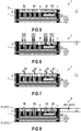
- a semiconductor module in which a chip is mounted on a metal composite substrate and bonded to a copper metal layer with a prepreg resin so that the chip is sandwiched between the metal composite substrate and the copper metal layer. Apertures are then etched into the copper metal layer, and the resin thereunder exposed is removed, leaving microvia openings that extend to a surface of the chip. Micro via connections are created in the micro via openings, which extend from terminals of the chip to the copper metal layer.
- KR 2010 0051291 A describes a method in which a metal foil, which has through openings and is attached to a carrier by means of a foam resin, is attached to an electronic element by means of a resin layer in such a way that the foam resin and the carrier are on the side of the metal foil remote from the electronic element . Thereafter, the foam resin and the carrier are removed, and the remaining metal foil provided with the through-holes is used as a mask to pattern the resin layer, thereby creating through-holes in which electrodes of the electronic element are exposed. The through holes are filled with electrically conductive material to create vias connecting the metal foil to the electrodes.
- JP S52 63672 A there is known an arrangement in which a double layer of a resin film and a heat-resistant resin substrate is disposed on a semiconductor element.
- the double layer has through holes, below which there are electrode pads of the semiconductor element.
- a metal layer extending into the through-holes and contacting the electrode pads is conformally deposited on the double layer provided with the through-holes.
- solder balls are positioned on the metal layer and then melted, so that the solder flows through the area of the through-holes located above the metal layer.
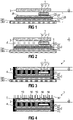
- One aspect relates to a method in which a first opening is produced in an assembly that has a first semiconductor chip, a metal plate, and a dielectric connecting compound that materially connects the first semiconductor chip and the metal plate.
- a first load electrode of the first semiconductor chip is exposed in a first portion of the first opening located in the connection ground.
- a first electrically conductive connection is created, which contacts the first load electrode exposed in the first portion of the first opening and is electrically conductive with the metal plate connects.
- a first substrate unit is produced, in which the first semiconductor chip is bonded to a first substrate.
- the first substrate has a dielectric insulation carrier which is designed as a flat plate and which has a first main surface and a second main surface opposite thereto, with a first substrate metallization being applied to the first main surface.
- a further aspect relates to a power semiconductor module which has an assembly with a first semiconductor chip, a metal plate and a dielectric connecting mass which materially connects the first semiconductor chip and the metal plate to one another.
- An electrically conductive connection which contacts the first load electrode and electrically conductively connects to the metal plate, extends through the connection ground.
- the first semiconductor chip is part of a first substrate unit, which has a first substrate and the first semiconductor chip which is materially bonded to the first substrate.
- the first substrate has an insulating dielectric support which is in the form of a flat plate and which has a first main surface and a second main surface opposite thereto. A first substrate metallization is applied to the first main area.
- the Figures 1 to 12 illustrate various steps of a method for producing a power semiconductor module, in which, in a composite in which a semiconductor chip and a metal plate are materially connected to one another by means of a dielectric connecting compound, a first load electrode of the semiconductor chip is exposed and electrically conductively connected to the metal plate by means of a connecting layer .
- FIG. 12 illustrates a method for producing a power semiconductor module, in which the composite is planarized at the connection layer and, as a result, a plurality of sections of the connection layer are isolated.
- the Figures 14 to 17 illustrate a method for manufacturing a power semiconductor module in which the composite is created using a prefabricated metal plate having one or more through openings.
- Figures 18 to 19 illustrate a method for producing a power semiconductor module, in which the assembly has a leadframe on which a power semiconductor chip is arranged.
- figure 20 illustrates a method of making a Power semiconductor module, in which the connection layer electrically contacts both a load electrode and a control electrode of a semiconductor chip of the power semiconductor module.
- Figures 21 and 22 illustrate a method for manufacturing a power semiconductor module in which, after forming the connection layer, a load electrode and a control electrode of a semiconductor chip of the power semiconductor module are exposed.
- the Figures 23 and 24 illustrate a method for manufacturing a power semiconductor module in which the metal plate has different thicknesses.
- the Figures 25 to 28 illustrate a method for manufacturing a power semiconductor module in which a contact plug is produced laterally next to the metal plate.
- FIG. 12 shows a power semiconductor module in which the metal plate has an anchoring structure in the form of a projection which engages in the connecting mass.
- FIG. 1 shows a power semiconductor module, in which the metal plate has an anchoring structure in the form of a recess, into which the connecting mass engages.
- the Figures 31 and 32 illustrate a first example of how a solidifiable mass can be used to produce the electrically conductive connection between the metal plate and an electrode of a semiconductor chip or an electrode of a substrate assembly.
- Figures 33 to 35 illustrate a second example of how a solidifiable mass can be used to produce the electrically conductive connection between the metal plate and an electrode of a semiconductor chip or an electrode of a substrate assembly.
- Figures 36 and 37 illustrate a third example of how a solidifiable mass can be used to produce the electrically conductive connection between the metal plate and an electrode of a semiconductor chip or an electrode of a substrate assembly.
- Figure 12 illustrates a fourth example of how a solidifiable mass can be used to establish the electrically conductive connection between the metal plate and an electrode of a semiconductor chip or an electrode of a substrate assembly.
- the Figures 39 to 43 illustrate various steps of a method for manufacturing multiple power semiconductor modules using a common metal plate.
- the Figures 44 to 48 illustrate various steps of a method for manufacturing a power semiconductor module having a plurality of substrate assemblies that are electrically connected to one another by means of a metal plate.
- figure 1 1 shows a cross section through a section of an arrangement with a semiconductor chip 1 and a metal plate 3 to be bonded to the semiconductor chip 1.
- the semiconductor chip 1 can be temporarily attached to an auxiliary carrier 200, for example by means of an adhesive layer 201.
- the semiconductor chip 1 is attached to the auxiliary carrier 200 indirectly via a substrate 2 and a connecting layer 25, which will be explained in more detail later.
- the metal plate 3 or one or more segments of the metal plate 3 are used for rewiring in the finished power semiconductor module.
- the metal plate 3 has a maximum thickness d3. This can be, for example, in the range from 100 ⁇ m to 2000 ⁇ m, or in the range from 100 ⁇ m to 500 ⁇ m.
- metal plates 3 with a maximum thickness d3 of less than 100 ⁇ m or more than 2000 ⁇ m can also be used.
- Metals (including alloys) with good electrical conductivity are suitable as the material for the metal plate 3 .
- the metal plate 3 may be made of, or contain at least 50% by weight of, exactly one or more than one of the following metals: copper (Cu); aluminum (Al); molybdenum (Mon); silver (Ag); Gold (Au).
- the metal plate 3 can have a multi-layer structure with at least two metal layers of different composition.
- the metal plate 3 can have two copper layers between which a molybdenum layer is arranged.
- the prefabricated semiconductor chip 1 was arranged on a prefabricated substrate 2 and was bonded to the prefabricated substrate 2 by means of a connecting layer 25 .
- the semiconductor chip 1 can be connected in an electrically conductive or electrically insulating manner to a metallic surface 2t of the substrate 2 by means of the connecting layer 25 .
- a unit in which a semiconductor chip 1 is arranged on a substrate 2 and is cohesively connected to the substrate 2 by means of a connecting layer 25 is also referred to below as a substrate assembly 28 .
- the connection layer 25 can be, for example, a layer of solder, a layer with a sintered metal powder, or an electrically conductive or electrically insulating adhesive layer.
- the auxiliary carrier 200 and the adhesive layer 201 are located on the side of the substrate 2 facing away from the semiconductor chip 1, and the side of the substrate 2 facing away from the semiconductor chip 1 adheres directly to the adhesive layer 201.
- the semiconductor chip 1 is therefore through the adhesive layer 201 indirectly bonded to the auxiliary carrier 200 via the substrate 2 and the connecting layer 25 .
- the semiconductor chip 1 could also adhere directly to the adhesive layer 201 on its side facing away from the metal plate 3 .
- the substrate 2 and the connection layer 25 could be omitted.
- the auxiliary carrier 200 and the adhesive layer 201 could also be omitted.
- the semiconductor chip 1 and the metal plate 3 are brought into a certain relative position to one another in order to produce a compound 7 in which the semiconductor chip 1 and the metal plate 3, as shown in the result in figure 3 shown to be connected firmly and cohesively to one another by means of a connecting compound 4 .
- the connecting mass 4 therefore extends continuously between the semiconductor chip 1 and the metal plate 3 in the finished composite 7.
- more than one semiconductor chip 1 on the The substrate 2 can be arranged and connected to the substrate 2 in a cohesive manner by means of a connecting layer 25 .
- This allows any circuits such as half-bridges, H-bridges, 3-phase converters, logic semiconductor chips, sensor chips to be integrated into the power semiconductor module to be produced.
- a flowable preliminary product 4' of the dielectric connecting compound 4 is introduced between the semiconductor chip 1 and the metal plate 3 and subsequently hardened to form a solid body which forms the connecting compound 4 and which extends continuously between the semiconductor chip 1 and the metal plate 3 and the semiconductor chip 1 and the Metal plate 3 cohesively connects with each other.
- the connecting mass 4 can, for example, contain a plastic or consist of a plastic. Suitable plastics are, for example, duroplastics, but also thermoplastics. Likewise, the connecting compound 4 can contain a cured resin-hardener mixture or consist of a cured resin-hardener mixture.
- the preliminary product 4 ′ of the connecting compound 4 can be flowable, so that it can be placed in the flowable state (for example by transfer molding or compression molding) between the semiconductor chip 1 and the metal plate 3 can be cast or injected when they are in the predetermined relative position to each other. Alternatively, it is also possible to first cast or inject the preliminary product 4' onto the semiconductor chip 1 (e.g.
- the not yet cured preliminary product 4' extends continuously between the semiconductor chip 1 and the metal plate 3 solid connecting compound 4 are cured.
- the connecting mass 4 can be highly filled with a filler.
- the preliminary product 4 ′ and thus also the connecting compound 4 can contain a filler made of dielectric grains which are admixed to the preliminary product 4 ′ and are therefore also part of the hardened connecting compound 4 .
- Materials with a low linear thermal expansion coefficient for example, are suitable as fillers.
- a connecting mass 4 with a high mechanical strength and a low linear thermal expansion coefficient can be achieved inexpensively.
- the thermal conductivity of the connecting compound 4 can be increased in comparison to an unfilled connecting compound 4 which consists only of a plastic or a resin.
- a filler that absorbs less moisture per volume than the plastic or resin can reduce the moisture absorption of the bonding compound 4 compared to an unfilled bonding compound 4 consisting only of plastic or resin.
- a coefficient of linear thermal expansion is considered low if it is less than 20 ppm/K, referred to a temperature of 18°C.
- suitable fillers are silicon dioxide, aluminum oxide, boron nitride, silicon nitride, aluminum nitride, diamond or glass.
- a filled plastic or resin is considered "highly filled” if the total amount of filler embedded in the plastic or resin has at least 60 percent by volume of the total volume of the plastic or the resin and the filler.
- adjustment projections eg pins
- the adjustment projections can be formed, for example, on the metal plate 3 and the adjustment openings on the auxiliary carrier 200 to which the semiconductor chip 1 is glued. Conversely, the adjustment openings can also be formed on the metal plate 3 and the adjustment projections on the auxiliary carrier 200. If the introduction of the precursor 4 'between the If the semiconductor chip 1 and the metal plate 3 is carried out by means of an injection molding process in which the semiconductor chip 1 and the metal plate 3 are inserted into an injection mold, adjustment openings and/or projections can also be attached to the injection mold. There is also the possibility of optically recognizing the position of the metal plate 3 and, if necessary, correcting it (for example by means of an automatic positioning device) so that it is in the desired position relative to the semiconductor chip 1 .
- the semiconductor chip 1 has a semiconductor body 10 made of a semiconductor base material, in which in particular p-conducting and n-conducting semiconductor zones can be contained in order to implement a power semiconductor component integrated into the semiconductor body 10 .
- the semiconductor chip 1 can also have any number of electrically conductive layers, such as metallization, silicide layers or layers made of doped polycrystalline semiconductor material (e.g. polycrystalline silicon), but also any number of dielectric layers, such as nitride layers (e.g. silicon nitride) or Oxide layers (e.g. silicon oxide), or passivation layers such as e.g. B. imide layers.
- the semiconductor base material can be any known semiconductor base material customary for the production of semiconductor components, for example any element semiconductors (e.g. silicon, germanium), any compound semiconductors (e.g. II-VI semiconductors such as zinc selenide or cadmium sulfide, III -V semiconductors such as gallium phosphide, gallium arsenide, indium phosphide, indium antimonide, or IV-IV semiconductors such as silicon carbide or silicon germanium).
- the semiconductor base material can also have a gallium nitride layer which is arranged on a silicon substrate or on a silicon carbide substrate.
- the semiconductor chip 1 can optionally be a “bare chip” in which the semiconductor body 10 is exposed.
- the connecting compound 4 can extend as far as the semiconductor body 10 and directly adjoin it.
- a first load electrode 11 and a second load electrode 12 are applied to the semiconductor body 10 .
- first load electrode 11 and a second Load electrode 12 are to be understood as electrodes between which a load path of the power semiconductor component integrated into the semiconductor body 10 is formed and through which a high load current can flow during operation of the semiconductor chip 1.
- a "load electrode” is one of two chip electrodes 11, 12, between which is formed a load path of the power semiconductor component integrated in the semiconductor body 10.
- the load path can be designed, for example, in such a way that a current of at least 5 A or even at least 50 A can permanently flow through it without destroying the power semiconductor component.
- the semiconductor chip 1 between the first load electrode 11 and the second load electrode 12 can have a voltage blocking capacity of we at least 600 V.
- the first load electrode 11 is always electrically conductively connected to the metal plate 3 by means of an electrically conductive connecting layer 31 .
- the first load electrode 11 and the second load electrode 12 are located on opposite surfaces of the semiconductor body 10 so that the semiconductor body 10 is arranged between the first load electrode 11 and the second load electrode 12 .
- the second load electrode 12 can be located anywhere in relation to the first load electrode 11 .
- the first load electrode 11 and the second load electrode 12 could also be arranged on the same surface of the semiconductor body 10 .
- the second load electrode 12 can be connected to the metal surface 2t in a materially bonded and electrically conductive manner by the connection layer 25 adjoining it and the metal surface 2t of the substrate 2 .
- the semiconductor chip 1 could also have a control electrode 13 .
- Examples with such a semiconductor chip 1 are in Figures 20 to 22 shown.
- the load path formed between the first load electrode 11 and the second load electrode 12 can be controlled via such a control electrode 13 .
- the load path can change into an electrically conductive or electrically conductive state blocking state.
- the control electrode 13 can be in the form of a gate electrode or a base electrode, for example.
- the first load electrode 11, the second load electrode 12 and, if present, the control electrode 13 can be thin metallization layers, for example. Such metallization layers can, for example, already be applied to the semiconductor body 10 during the production of the semiconductor chip 1, when the semiconductor chip 1 is still in the wafer assembly with other semiconductor chips 1, i.e. before the wafer is separated into semiconductor chips 1 that are independent of one another and thus also before the semiconductor chip 1 is cohesively connected to the metal plate 3 by the connecting compound 4 . Accordingly, the first load electrode 11, the second load electrode 12 and the control electrode 13 can also be referred to as "chip electrodes". The first load electrode 11, the second load electrode 12 and (if present) the control electrode 13 can each be metal layers.
- the materials of the first load electrode 11, the second load electrode 12 and the control electrode 13 can be chosen independently of one another.
- the layer thicknesses of the first load electrode 11 and the second load electrode 12 are in principle arbitrary and they can be selected independently of one another.
- the layer thickness of the first load electrode 11 can be at least 2 ⁇ m, at least 10 ⁇ m or even at least 20 ⁇ m.
- Suitable materials for the first load electrode 11, the second load electrode 12 and (if present) the control electrode 13 are metals including alloys, but also other electrical conductors.
- a first load electrode 11 and a second load electrode 12, independently of one another, can each have or consist of one of the following materials: copper; Aluminum; copper and aluminum.
- the first load electrode 11 can include or consist of copper, while the second load electrode 12 can be free of copper.
- the power semiconductor component can be a vertical or a lateral power semiconductor component. It is pointed out that the semiconductor chip 1 is not limited to the examples mentioned.
- the first load electrode 11 and the second load electrode 12 can be, for example, a source and a drain electrode, or a drain and a source electrode, or a collector and a collector, depending on the type of component emitter electrode, or around an emitter and a collector electrode, or around an anode and a cathode electrode, or around a cathode and an anode electrode.
- Both the first load electrode 11 and the second load electrode 12 can be different from a control electrode, in particular different from both a gate electrode and different from a base electrode.
- the metal plate 3 can be structured in such a way that it has one or more through-openings 30, which later - in each case forming a Section 40 of the opening 60 to be produced, to the openings 60 to be produced ( figure 7 ) to be expanded.
- figure 5 shows the arrangement after the production of the through-openings 30.
- the through-openings 30 can be produced, for example, by means of a masked etching process, which is shown in FIG figure 4 is shown schematically.
- a structured etching mask layer 5 is produced on a surface of the metal plate 3, which has one or more mask openings 50.
- FIG. The metal plate 3 is exposed in each mask opening 50, so that during the etching process an etchant 301 reaches the metal plate 3 through the mask opening 50 and locally removes the material of the metal plate 3 in the area of the mask opening 50, so that a through-opening is formed in the metal plate 3 30 arises, which forms a portion of the opening 60 to be produced.
- the through hole 30 extends continuously between two opposite surfaces of the metal plate 3.
- Suitable etching methods are, for example, anisotropic etching methods such as (reactive ion etching; "RIE"), or isotropic etching processes with a liquid etchant.
- RIE reactive ion etching
- a through opening 8 is produced which separates the metal plate 3 into two or more segments, which results in figure 6 is shown.
- the structured mask layer 5 can be produced in any way, for example photolithographically, by means of LDI (laser direct imaging), etc., which is known per se and is therefore not explained in more detail.
- the mask layer 5 is formed in such a way that it is etch-resistant to the etchant used to locally remove the material of the metal plate 3, or at least has a lower etch rate to the etchant than the material of the metal plate 3.
- the through-openings 30 are produced in a state in which the metal plate 3 is already materially connected to the semiconductor chip 1 by the connecting compound 4 .
- the mask layer 5 is produced on that surface of the metal plate 3 which is remote from the semiconductor chip 1 .
- a masked etching method can also be used here, as was previously described.
- the etching mask layer 5 can be produced on the surface of the metal plate 3 which faces away from the semiconductor chip 1 in the composite 7 produced later, but also on the surface of the metal plate 3 which faces the semiconductor chip 1 in the composite 7 produced later.
- a section 40 can be produced in the connecting compound 4 for one or more openings 60 to be produced in such a way that the same first load electrode 11 is exposed in each of these sections 40 and thus in the corresponding openings 60 .
- the Figures 6 and 7 12 only show two such sections 40 (and thus two openings 60) by way of example, in which the same first load electrode 11 is exposed in each case.
- the number such sections 40 (and thus the number of such second openings 60) in which the same first load electrode 11 is exposed is fundamentally arbitrary.
- one or more further sections 40 can optionally be produced in the connecting mass 4 in such a way that the substrate 2 is exposed therein in each case.
- the Figures 6 and 7 12 only show two such further sections 40 by way of example. If one or more such further sections 40 are produced, their number is fundamentally arbitrary. If sections 40 or further sections 40 are provided, they can each extend continuously between two opposite surfaces of the connecting compound 4 , so that the section 40 in question forms a through-opening in the connecting compound 4 .
- one or more sections 40 can be generated in any desired manner.
- the sections 40 can be produced simultaneously or in succession in the case of two or more sections 40 .
- the sections 40 are produced in that the connecting mass 4 is opened locally by means of a laser beam 302 .
- the through-openings 30 formed in the metal plate 3 can be used as mask openings and the metal plate 3 can therefore be used as a mask for the laser beam 302, so that the laser beam 302 only removes material of the connecting compound 4 in those areas in which it passes through the through-openings 30 onto the Connection mass 4 hits.
- the presentation according to figure 6 is only intended to illustrate that the metal plate 3 can be used as a mask for the laser beam 302 .
- the laser beam 302 must be sized to simultaneously detect two or more through holes 30 .
- the laser beam 302 can be dimensioned in such a way that it is able to produce a section 40 in the area of only one through opening 30 .
- the laser beam 302 can then be moved successively from one through-opening 30 to another through-opening 30 and thereby generate a corresponding section 40 in the region of the respective through-opening 30, so that the through-opening 30 and the corresponding section 40 form sections of an opening 60, in which the first load electrode 11 is exposed, resulting in figure 7 is shown.
- one or more further openings 60 are produced, in which an electrically conductive surface 2t of the substrate 2, for example an electrically conductive surface 2t of a conductor track of the substrate 2, is exposed, which as a result also results in figure 7 is shown.
- a through opening 30 and a section 40 can thus together form an opening 60 in which the first load electrode 11 or a metallic surface of the substrate 2 is exposed.
- no or essentially no material of the connecting mass 4 is removed by the laser beam 302 .
- an electrically conductive connecting layer 31 is produced on the composite 7, which contains the semiconductor chip 1, the metal plate 3 and the connecting mass 4, which layer 31 is formed in the section 40 or makes electrical contact with the first load electrode 11 of the semiconductor chip 1 that is exposed in the opening 60 and electrically connects it to the metal plate 3 .
- the connecting layer 31 can also make electrical contact with an exposed metallic surface 2t of the substrate 2 in a further section 40 or in an opening 60 belonging to this section 40 and electrically connect it to the metal plate 3 .
- the connecting layer 31 can be, for example, a metal layer or a layer made of or with another material with good electrical conductivity.
- the electrically conductive connecting layer 31 can be produced, for example, by depositing the material forming the electrically conductive connecting layer 31 on the composite 7 containing the semiconductor chip 1, the metal plate 3 and the connecting compound 4 by means of a chemical and/or physical deposition process.
- Suitable deposition methods are, for example, chemical deposition methods such as chemical vapor deposition ("CVD") or electroless chemical deposition, or physical deposition methods such as physical vapor deposition (PVD) such as vapor deposition, spin-on, sputtering.
- CVD chemical vapor deposition
- PVD physical vapor deposition
- a conformal deposition process can be used as the deposition process.
- connection layer 31 By creating the connection layer 31, the required electrical connections between the metal plate 3 and the first load electrode 11 and optionally also between the metal plate 3 and a metal surface 2t of the substrate 2, so that the power semiconductor module can already be used. According to the example shown figure 8 the connection layer 31 does not completely fill the section 40 and thus the opening 60 . In order to increase the current-carrying capacity of the electrical connections between the metal plate 3 and the first load electrode 11 and, if provided, between the metal plate 3 and the substrate 2 caused by the connecting layer 31, the section 40 and optionally also the opening 60 can go completely through the connecting layer 31 to be filled, resulting in figure 9 is shown. In the area of an opening 60, the connecting layer 31 then forms a solid contact plug 310.
- a section of the connecting layer 31 runs through the opening 60, contacts the first load electrode 11 exposed in the opening 60 and connects it electrically conductively to the metal plate 3.
- the connection layer 31 ie before any subsequent planarization or other partial removal of the deposited connection layer 31
- any subsequent planarization or other partial removal of the deposited connection layer 31 ie in particular also in the case of the fully processed power semiconductor module.
- whose layer thickness d31 is, for example, in the range from 20 ⁇ m to 100 ⁇ m. In principle, however, layer thicknesses d31 of less than 20 ⁇ m or more than 100 ⁇ m are also possible.
- connection layer 31 can be designed so that its effective length required for making the electrical connection of the metal plate 3 with an electrode 11, 21 of a semiconductor chip 1 or substrate 2 or a substrate assembly 28 is very short, and there if necessary two or more sections of the connecting layer 31 (i.e. two or more contact plugs 310) can be connected electrically in parallel if a certain current-carrying capacity is to be achieved, the layer thickness d31 of the connecting layer 31 can be selected to be smaller than the maximum thickness d3 of the metal plate 3.
- connection layer 31 has a flat surface
- connection layer 31 can also be planarized on its surface facing away from the semiconductor chip 1, which results in figure 10 is shown.
- suitable Planarization methods are, for example, grinding, polishing or lapping.
- the metal plate 3 can be uncovered in the areas in which it was covered by the connecting layer 31 after the end of the deposition process by locally removing the connecting layer 31 and different contact plugs 310 can be isolated, which results in figure 11 is shown.
- the exposure can in turn be effected by means of a planarization method such as grinding, polishing or lapping, in which the composite 7 comprising the semiconductor chip 1, the metal plate 3, the connecting compound 4 and the electrically conductive connecting layer 31 is removed from the side on which the connecting layer 31 is located , is planarized.
- the connecting layer 31 can consist of one material, e.g. a metal, or a material mixture, e.g. a mixture of or with at least two different metals. Suitable materials which have such a connecting layer 31 or from which such a connecting layer 31 can consist are, for example, copper (Cu), molybdenum (Mo), aluminum (Al), nickel (Ni), tin (Sn) or silver (Ag ).
- a connecting layer 31 it is also possible for a connecting layer 31 to have two or more partial layers 31′, 31′′ made of different materials or different material compositions.
- a first partial layer 31′ can be produced, as described with reference to FIG figure 8 for the connection layer 31 has been explained.
- a second partial layer 31" of the connecting layer 31 can be produced directly on such a first partial layer 31', as is shown in figure 10 is shown.
- the second partial layer 31′′ can be produced by galvanic deposition in a galvanic bath, with the first partial layer 31′′ being used as an electrode for the galvanic process.
- a dielectric mask 81 can be produced on the first partial layer 31' in the area of the through-opening 8, which mask 81 prevents galvanic deposition in the area of the mask 81, what result in figure 10 is shown.
- the first partial layer 31' directly contacts both the first load electrode 11 and the metal plate 3, and, optionally, the substrate 2 (in particular a metallic surface 2t of the substrate 2). Accordingly, the first partial layer 31' also assume the function of an adhesion promoter.
- Suitable materials which have such a first partial layer 31' or from which such a first partial layer 31' can consist are, for example, titanium (Ti); tungsten (W); tantalum (Ta); titanium tungsten ( TiW).
- Suitable materials for a second partial layer 31" applied directly to a first partial layer 31' are, for example, copper (Cu), molybdenum (Mo), aluminum (Al), nickel (Ni), tin (Sn) or silver (Ag ).
- a connecting layer 31 has two sub-layers 31', 31" it can consist of exactly one first sub-layer 31' and one second sub-layer 31", or it can have two or more sub-layers 31', 31".
- this can have a layer thickness d31' (see figure 8 ) have, for example, less than 10 microns. However, layer thicknesses d31' of 10 ⁇ m or more are also possible.
- the layer thickness d31 of the connecting layer 31 can be in the range from 20 ⁇ m to 100 ⁇ m, for example. In principle, however, layer thicknesses d31 of less than 20 ⁇ m or more than 100 ⁇ m are also possible.
- a connecting layer 31 can also be additionally produced on the surface of the composite 7 facing away from the metal plate 3 .
- the first partial layer 31′ could also be produced on the surface of the composite 7 facing away from the metal plate 3 and, optionally, the second partial layer 31′′ could also be produced on the side of the supplementary first partial layer 31′ that faces away from the semiconductor chip 1 Figures 8 to 13 the supplementary first sub-layer 31' and the supplementary second sub-layer 31'' are shown in dashed lines.
- the mask 81 together with a section of the first located in the area of the mask 81 Sublayer 31' are removed, so that the segments of the metal plate 3 electrically connected by this section of the first sublayer 31' are electrically separated again, which can be done, for example, by means of an etching process.
- a small part of the second partial layer 31'' can also be removed during the etching process.
- figure 11 shows the arrangement after the etching process.
- through-opening 8 can optionally be filled with a dielectric compound 4", for example in order to increase the insulating strength between the segments of metal plate 3 separated by through-opening 8, which results in figure 12 is shown.
- the through-openings 30 were produced in the metal plate 3 in a state in which the metal plate 3 was already cohesively connected to the semiconductor chip 1 by the connecting compound 4, is explained below with reference to FIG Figures 14 to 17 a method is explained in which a metal plate 3 is used, which already has one or more through-openings 30 at a time when the metal plate 3 is not yet firmly connected to the semiconductor chip 1 by the connecting compound 4, as is the case in figure 14 is shown.
- These one or more through openings 30 can be produced, for example, by means of an etching method in which a metal plate 3 that is not yet connected to the semiconductor chip 1 is etched in a structured manner, as has already been described with reference to FIG figures 4 and 5 was explained.
- the one or more through-openings 30 can also be produced by using the metal plate 3, which is not yet connected to the semiconductor chip 1
- the substrate 2 can have at least one metallic surface 2t.
- the substrate 2 has a dielectric insulating support 20 which is in the form of a flat plate and which has a first main surface and a second main surface opposite thereto.
- a first substrate metallization 21 is applied to the first main surface, which can optionally be structured to form interconnects that are spaced apart from one another.
- an optional second substrate metallization 22 can be applied to the second main surface.
- the second substrate metallization 22 is unstructured, but it can alternatively also be structured.
- the metallic, electrically conductive surface 2t of the substrate 2 is formed by the surface of the first substrate metallization 21 facing away from the insulating support 20 .
- the substrate metallizations 21 and 22 are firmly, extensively and cohesively connected to the insulation carrier 20 .
- the first substrate metallization 21 can be firmly and cohesively connected to the insulation carrier 20 over its entire side facing the insulation carrier 20 .
- the second substrate metallization 22 (if present) can also be firmly and cohesively connected to the insulation carrier 20 over its entire side facing the insulation carrier 20 .
- the insulating support 20 is electrically insulating.
- it can have ceramic or consist of ceramic. Suitable ceramics are, for example, aluminum oxide (Al 2 O 3 ), silicon nitride (Si 3 N 4 ), aluminum nitride (AlN), or other dielectric ceramics.
- the first substrate metallization 21 and, if present, the second substrate metallization 22 can consist, for example, of copper, a copper alloy, aluminum or an aluminum alloy, or have one of these materials. However, other electrically highly conductive metals including alloys can also be used.
- the first substrate metallization 21 and, if present, the second substrate metallization 22 can each have two or more partial layers, each of which consists of a metal or a metal alloy.
- DCB direct copper bonded
- an optional second substrate metallization 22 can be applied to the second main surface.
- the second substrate metallization 22 is unstructured, but it can alternatively also be structured.
- the metallic, electrically conductive surface 2t of the substrate 2 is formed by the surface of the first substrate metallization 21 facing away from the insulating support 20 .
- the substrate metallizations 21 and 22 are firmly, extensively and cohesively connected to the insulation carrier 20 .
- the first substrate metallization 21 can be firmly and cohesively connected to the insulation carrier 20 over its entire side facing the insulation carrier 20 .
- the second substrate metallization 22 (if present) can also be firmly and cohesively connected to the insulation carrier 20 over its entire side facing the insulation carrier 20 .
- the insulating support 20 is electrically insulating.
- it can have ceramic or consist of ceramic. Suitable ceramics are, for example, aluminum oxide (Al 2 O 3 ), silicon nitride (Si 3 N 4 ), aluminum nitride (AlN), or other dielectric ceramics.
- the first substrate metallization 21 and, if present, the second substrate metallization 22 can consist, for example, of copper, a copper alloy, aluminum or an aluminum alloy, or have one of these materials. However, other electrically highly conductive metals including alloys can also be used.
- the first substrate metallization 21 and, if present, the second substrate metallization 22 can each have two or more partial layers, each of which consists of a metal or a metal alloy.
- At least one of the copper foils can be structured to form conductor tracks and/or conductor surfaces after it has been connected to the insulating carrier 20 .
- a copper foil Before or after the structuring, a copper foil can be provided with a thin metallic coating on its side facing away from the insulation carrier 20, for example in order to improve the solderability.
- a thin metallic coating may, for example, comprise or consist of one of the following materials: nickel (Ni); gold (Au); silver (Ag); Platinum (Pt).
- the insulation carrier 20 does not necessarily have to be made of ceramic. Rather, non-ceramic, electrically insulating materials such as, for example, resins, which are highly filled with a filler, can also be used as the insulating support 20 .
- non-ceramic, electrically insulating materials such as, for example, resins, which are highly filled with a filler, can also be used as the insulating support 20 .
- granular dielectric fillers with a low relative dielectric constant are suitable as fillers, for example if high switching speeds are to be achieved. In this sense, a relative dielectric constant is considered low if it is less than 5, referred to a temperature of 18°C and a frequency of 50 Hz.
- suitable fillers are silicon dioxide, aluminum oxide, boron nitride, silicon nitride, aluminum nitride, diamond or glass.
- a filled resin is considered "highly filled" when the total amount of filler embedded in the resin is at least 60 percent by volume of the total
- a metallic conductor frame can also be used as the substrate 2, which has a metallic, electrically conductive surface 2t.
- a leadframe can consist of a single metal segment. However, it can also have two or more separate metal segments. It is likewise possible for the lead frame to initially have only one metal segment, which is separated into two or more from one another during the manufacturing process of the power semiconductor module separate metal segments is isolated.
- the semiconductor chip 1 can, as already with reference to figure 1 explained, by means of a connecting layer 25 to the substrate 2 (for example, to a metallic surface 2t of the substrate 2) in a materially bonded and electrically conductive or electrically insulating manner.
- a power semiconductor module can be produced according to any of the variants explained above.
- figure 19 shows an example of a power semiconductor module whose structure, apart from the different substrate 2, in figure 13 corresponds to the structure explained.
- the connection layer 31 can optionally connect the metal plate 3 directly and electrically conductively to the metal surface 2t of the leadframe 2.
- a semiconductor chip 1 can also have a control electrode 13, by means of which the load path formed between the first load electrode 11 and the second load electrode 12 can be controlled, which has already been explained above.
- the first load electrode 11 and the control electrode 13 are applied to the same surface of the semiconductor body 10 facing away from the substrate 2 , while the second load electrode 12 is applied to the surface of the semiconductor body 10 facing the substrate 2 .
- the control electrode 13, like the first load electrode 11, can be electrically conductively connected to the metal plate 3 with the aid of the electrically conductive connecting layer 31.
- the first load electrode 11 can be electrically conductively connected to a first section 311 of the metal plate 3 by means of a first section of the connection layer 31, and the control electrode 13 can be electrically conductively connected to a second section 312 of the metal plate 3 that is separate from the first section 311 by means of a second section of the connecting layer 31 .
- the metal plate 3 and the connection layer 31 do not cause an electrically conductive connection between the first load electrode 11 and the control electrode 13.
- the first section 311 and the second section 312 of the metal plate 3 can be separated from one another be separated after the metal plate 3 has already been cohesively connected to the semiconductor chip 1 by the connecting compound 4, which simplifies handling.
- the etching step explained takes place when the etching mask 5 is provided with a further opening 50 in such a way that the etchant 301 separates the first section 311 and the second section 312 during the subsequent etching step. Since the subsequent creation of the connecting layer 31 again causes an undesired electrical short circuit between the first section 311 and the second section 312, it is expedient if the connecting layer 31 is removed again at least to the extent that the first section 311 and the second section 312 no longer electrically connected.
- the local removal of the connecting layer 31 can optionally be carried out by means of a planarization process such as grinding, polishing or lapping, in which the composite 7 comprising the semiconductor chip 1, the metal plate 3, the connecting compound 4 and the electrically conductive connecting layer 31 is on the side on which the connection layer 31 is located, is planarized.
- the semiconductor chip 1 and the substrate 2 were each arranged on an auxiliary carrier 200 by means of an adhesive layer 201 at the beginning of the method until after the curing of the flowable preliminary product 4′ forming the connecting means 4.
- the adhesive layer 201 and the auxiliary carrier 200 can be removed from the assembly 7 at any time, see above that the substrate 2 is exposed.
- the adhesive layer 201 and the auxiliary carrier 200 can be removed from the composite 7 before each of the planarization steps explained.
- the semiconductor chip 1 was by means of a connecting layer 25 cohesively connected to a substrate 2, which is part of the finished power semiconductor module. As below with reference to the Figures 21 and 22 is explained, however, a semiconductor chip 1 does not necessarily have to be arranged on a substrate 2 .
- the first load electrode 11 and the second load electrode 12 can be applied to opposite surfaces of the semiconductor body 10.
- FIG. The semiconductor chip 1 can then be glued to the submount 200 at the second load electrode 12 using the adhesive layer 201 so that the semiconductor chip 1 is fixed to the submount 200 .
- the integral connection of the semiconductor chip 1 to the metal plate 3 by means of the connecting means 4 and all other steps explained with reference to the previous examples can be carried out in the same or analogous manner, unless they require the presence of a substrate 2.
- the semiconductor chip 1, as also in figure 21 shown have a control electrode 13 which is applied to the same surface of the semiconductor body 10 as the second load electrode 12.
- the semiconductor chip 1 is also glued to the control electrode 13 using the adhesive layer 201 on the auxiliary carrier 200.
- the adhesive layer 201 and the auxiliary carrier 200 can be removed from the assembly 7 at any time, see above that the second load electrode 12 and, if present, the control electrode 13, as in figure 22 is shown, are exposed and can be electrically contacted. Therefore, the second load electrode 12 and, if present, the control electrode 13 are not or at least not completely covered by the connecting ground 4 .
- the prefabricated metal plate 3 can have different thicknesses before it is materially connected to the semiconductor chip 1 by the connecting compound 4 .
- Such a configuration can be used, for example, to save material costs and weight when the finished power semiconductor module from the prefabricated metal plate 3 has sections 35 produced for which a smaller thickness d35 is sufficient than for other sections produced from the prefabricated metal plate 3 in order to achieve the required current-carrying capacity.
- a metal plate 3 with different thicknesses can be produced in a simple manner, for example by embossing or milling a flat metal plate having a constant thickness.
- the metal plate 3, which has sections of different thicknesses, can be materially bonded to the semiconductor chip 1 by means of a dielectric bonding compound 4 in accordance with any of the methods explained above, with the semiconductor chip 1 optionally by means of a bonding layer 25, likewise as explained above, being materially bonded to any substrate 2 can be connected.
- figure 24 shows the arrangement after the semiconductor chip 1 has been materially connected to the metal plate 3 by the connecting compound 4 .
- the metal plate 3 can have one or more through-openings 30 from one or more openings 60 to be produced before it is materially connected to the semiconductor chip 1 by the connecting compound 4 .
- one or more through-openings 30 can also be produced in the metal plate 3 after the semiconductor chip 1 has been connected to the metal plate 3 with a material fit by the connecting compound 4 .
- the use of a metal plate 3, which has different thicknesses d3, d35, can be implemented in any of the methods explained above.
- a thin section 35 of the metal plate 3, which has a thickness that is less than the maximum thickness d3 of the metal plate 3, can be connected to a control terminal 13 of the semiconductor chip 1 via the connection layer 31 in order to supply an electrical drive potential to it.
- the use of a thin section of the metal plate 3, which has a thickness that is less than the maximum thickness d3 of the metal plate 3, can generally make sense if the smaller thickness is sufficient for the section with the smaller thickness to have the required current-carrying capacity.
- a laser beam 302 can produce an opening 60 laterally next to the metal plate 3 in the connecting mass 4, which has no through-opening 30 formed in the metal plate 3, and which extends up to the first load electrode 31, so that the first load electrode 11 in the section 40 (and thus in the opening 60) is exposed.
- the section 40 then forms the opening 60.
- a connecting layer 31 can be produced on the semiconductor chip 1, the metal plate 3 and the composite 7, which connects the semiconductor chip 1 and the metal plate 3 in a materially bonded manner
- Figures 27 and 28 is shown, purely by way of example, for a connecting layer 31, which has a first partial layer 31' and a second partial layer 31" applied directly to the first partial layer 31'.
- a contact plug 310 produced according to the present example can be produced in combination with any other contact plug 310 which, as explained in the previous examples, is characterized by an in the through hole 30 formed in the metal plate 3 extends therethrough.
- a metal plate 3 can have one or more anchoring structures 33 on which the connecting mass 4 can claw, which leads to an improved connection between the metal plate 3 and the connecting mass 4 .
- an anchoring structure 33 can be formed as a projection of the metal plate 3 while figure 30 shows that an anchoring structure 33 can also be designed as a recess in the metal plate 3 .
- An anchoring structure 33 can optionally also have an undercut.
- the geometry of a as a protrusion or indentation formed anchoring structure 33 of the metal plate 3 and the position of an anchoring structure 33 on the metal plate 3 can be chosen arbitrarily, as long as the anchoring structure 33 is in physical contact with the connecting mass 4.
- Another possibility, alternative or supplementary to an anchoring structure 33, to increase the strength of the connection between the metal plate 3 and the connecting mass 4 consists in that surface of the metal plate 3 which faces the semiconductor chip 1 in the finished power semiconductor module (i.e. the surface , which has the largest contact area with the connecting compound 4, before the flowable preliminary product 4' of the dielectric connecting compound 4 is introduced between the semiconductor chip 1 and the metal plate 3.
- an electrically conductive connecting layer 31 can be produced using a single-stage or multi-stage deposition process.
- another example illustrates how an electrically conductive bond layer can be made using a solidifiable electrically conductive mass 34' that is placed in one or more of the openings 60 and subsequently solidified.
- the solidified, likewise electrically conductive mass is identified by reference number 34 in each case.
- the electrically conductive mass forms the connecting layer 31 in whole or in part.
- solidification can take place by at least one of cooling, hardening and sintering.
- the solidifiable mass 34' can optionally be introduced in such a way that the solidifiable electrically conductive mass 34' makes both electrical and physical contact with at least the first load electrode 11 exposed in one of the openings 60 and the metal plate 3.
- the solidifiable electrically conductive mass 34 ′ is pressed into the one or more openings 60 , which is done by means of a squeegee 500 , for example.
- a squeegee 500 for example.
- the solidifiable electrically conductive mass 34' could be injected locally into the individual openings 60 by means of a nozzle. After the solidifiable electrically conductive mass 34' has been introduced into the at least one opening 60, the mass 34' is solidified, which results in figure 32 is shown.
- the solidifiable electrically conductive mass 34' can be, for example, a solder paste, or a paste that contains a metal powder and a solvent (e.g. a sintering paste that contains a metal powder and a solvent, or an adhesive compound that contains a metal powder ).
- a solder the solder introduced into the at least one opening 60 is melted and subsequently cooled to below its solidus temperature, so that it solidifies.
- the paste introduced into the at least one opening 60 is solidified by partial or complete evaporation of the solvent.
- the partial or complete evaporation of the solvent is followed by a temperature step in which the metal powder remaining in the at least one opening 60 is sintered.
- the remaining metal powder is solidified by the particles of the metal powder being fixed relative to one another during sintering.
- the sintering can optionally take place without pressure, ie without an external pressure being exerted on the metal powder remaining in the at least one opening 60 during the temperature step.
- pressureless sintering sintering can also be carried out by subjecting the metal powder remaining in opening 60 to pressure during the temperature step and thereby compressing it.
- the arrangement in a deformable cover (eg a film or a gel cover) and then (e.g. via a liquid) is isostatically pressurized (e.g. by hot isostatic pressing) that is greater than the ambient pressure (e.g. at least 1 MPa bar absolute), so that the isostatic pressure indirectly compresses the remaining metal powder via the envelope.
- a deformable cover e.g. a film or a gel cover
- the ambient pressure e.g. at least 1 MPa bar absolute
- the composite 7 can be placed in an oven that generates the temperature required for sintering.
- the metal powder remaining in the at least one opening 60 can also be sintered by laser sintering.
- a meltable (and thus solid) electrically conductive starting material 34" can be placed above the at least one opening 60 and then melted to form a solidifiable electrically conductive material 34', so that it flows into the openings 60. Thereafter, the into the openings 60 located solidifiable electrically conductive mass 34 'are solidified by cooling to below their solidus temperature to the solid mass 34, resulting in figure 34 is shown. Excess sections of the solidified mass 34 can, as already explained and as a result in figure 35 shown, be removed to avoid unwanted short circuits.
- the fusible electrically conductive starting material 34" extends continuously (e.g. in the form of a small plate such as a small solder plate) across two or more of the openings 60
- a starting mass particle 34" can be, as in figure 36 shown to be eg a sphere, but also another body.
- a rod-shaped starting material particle 34" could also be inserted into one or more of the openings 60.
- Another alternative possibility is to fill one or more of the openings 60 with a plurality of starting material particles 34" in the form of a powder.
- the initial mass particles 34" After the initial mass particles 34" have been placed in the position explained in each case, they are melted to form a solidifiable mass 34' solidifiable electrically conductive mass 34' located in the openings 60 can be solidified to form the solid mass 34 by cooling to below its solidus temperature, which results in figure 37 .
- the starting mass 34" was dimensioned such that the openings 60 were completely filled by the solid mass 34. Deviating from this, the starting mass 34" could also be dimensioned such that the openings 60 were not completely filled by the solid mass 34. Also with the based on the Figures 36 and 37 Excess portions of the solidified mass 34 can optionally be removed.
- solidified mass 34 provided direct physical and electrical contact between metal plate 3 and load electrode 11 exposed in one of openings 60, and optionally also between the metallic surface of substrate 2 exposed in one of openings 60.
- the solidified mass 34 can also be produced in such a way that it rests directly on one or more deposited partial layers 31′, at least in the openings 60, as explained above.
- the composite 7 has at least one partial layer 31′ before the fusible starting mass 34′′ is placed.
- the solidified mass 34 can be produced as described with reference to FIG Figures 31 to 37 was explained, with the difference that before placing the solidifiable mass 34' and, if applicable, before placing the electrically conductive starting mass 34", one or more deposited sub-layers 31' were produced, as was described above with reference to FIGS Figures 1 to 30 has been explained, with the proviso that the one or more deposited sub-layers 31 'do not completely fill the openings 60. If a solidified, electrically conductive mass 34 is produced on one or more partial layers 31', the one or more partial layers 31' and the electrically conductive mass 34 are components of the connecting layer 31.
- a connecting layer 31 can be used to create at least one electrically conductive connection between a metal plate 3 and a first load electrode 11 of a semiconductor chip 1, and how the same connecting layer 31 can optionally also be used to produce at least one further electrically conductive connection between the same metal plate 3 and a further electrical element (e.g. a first substrate metallization 21 or a substrate 2 designed as a leadframe). It was also explained how the metal plate 3 can optionally be divided into two or more segments that are separate from one another, so that such a segment forms a conductor track that can be used in any way for the electrical interconnection of the power semiconductor module.
- a segment of the metal plate 3 in cooperation with one or more contact plugs 310 can replace a bonding wire, e.g it is used in conventional power semiconductor modules, so that the problems described at the outset that occur when using bonding wires are avoided.
- a segment of the original metal plate 3 can be electrically connected to a first load electrode 11 of a semiconductor chip 1 or to a substrate 2 by means of a connecting layer 31, so that the first load electrode 11 and the substrate 2 are permanently electrically conductively connected to one another are.
- a segment of the metal plate 3 it is also possible for a segment of the metal plate 3 to be electrically connected to the first load electrode 11 by means of at least one contact plug 310 and to the substrate 2 by means of at least one further contact plug 310 .
- Bond wires are understood to mean wires that are bonded directly to a metallization (for example an electrode 11, 12, 13 of a semiconductor chip 1 or a metallization 21, 22 of a substrate 2) by wire bonding, by a short section of the bonding wire being bonded by means of a bonding tool is pressed directly onto the metallization so that the bonding wire in the section in question enters into a cohesive and firm connection with the metallization, without the use of an additional connection means such as a solder or an adhesive. Such a connection is also referred to as a wire bond connection.
- a finished power semiconductor module produced by a method according to the present invention may generally not have a wire bond connection, or at least have no wire bond connection until the time at which the metal plate 3 is connected to the semiconductor chip 1 by means of the connecting compound 4 in a materially bonded manner.
- a power semiconductor module produced using a method according to the present invention may have one or more wire bond connections or to be electrically connected to module-external components, devices or arrangements by one or more wire bond connections.
- the bonding wires used in conventional power semiconductor modules are usually bonded sequentially to the required metallizations, this involves a great deal of time.
- the present invention allows for a significant time saving since the contact plugs 310 can be fabricated simultaneously.
- the metal plate 3 which can easily be designed in such a way that it has a significantly higher thermal capacity compared to bonding wires, as used in a conventional power semiconductor module with the same electrical functions and the same power class, so that the power semiconductor module has a higher thermal shock resistance has than a conventional power semiconductor module.
- the significantly higher heat capacity means that temperature fluctuations, such as those that occur in a semiconductor chip 1 during alternating switching operation, which is typical for power semiconductor modules, are less severe, so that the difference between the maximum chip temperature and the minimum chip temperature is smaller than in a conventional power semiconductor module (same electrical load provided).
- the metal plate 3 results in heat spreading and, as a result, better cooling than in FIG conventional power semiconductor modules.
- two or more power semiconductor modules can be manufactured simultaneously using a common metal plate and subsequently separated.
- the example shown is based on the example according to the Figures 1 to 9 .
- At least one semiconductor chip 1 was arranged on two or more prefabricated separate substrates 2 and connected to the prefabricated substrate 2 by means of a connecting layer 25 in a materially bonded manner.
- Each of these semiconductor chips 1 was bonded to a single metal plate 3 by the same dielectric bonding compound 4, and a structured etching mask layer 5 was produced on the surface of the metal plate 3 in such a way that one of the mask openings 50 (in figure 39 if this is the middle one of the mask openings) is located above a gap between adjacent substrates 2.
- a through-opening 9 is produced in the metal plate 3, which separates the metal plate 3 into two or more segments, which results in figure 40 is shown, the rest with figure 6 corresponds.
- the through-opening 9 can optionally be filled simultaneously with one or more through-openings 8 with a dielectric mass 4", as described with reference to FIG Figures 8 to 13 was explained for the through-opening 8, which resulted in figure 41 is shown.
- the through-opening 9 is positioned in such a way that the assembly 7 can be separated into two (or more) power semiconductor modules 400 by sawing using a planar cut that does not pass through any metallic parts, as shown in FIG Figure 42 is shown. The sawing can be done by means of a saw blade 300, for example.
- Figure 43 shows the two isolated power semiconductor modules 400.
- two or more separate substrates 2 or two or more separate from each other Substrate assemblies 28 are electrically connected to one another by the metal plate 3 based on a method as explained above.
- At least one semiconductor chip 1 was arranged on two or more prefabricated separate substrates 2 and bonded to the prefabricated substrate 2 by means of a connecting layer 25, so that two or more substrate assemblies 28 separate from one another are present.
- they can be temporarily attached to an auxiliary carrier 200, for example by means of an adhesive layer 201.
- a flowable precursor 4 'of the dielectric compound 4 introduced ( figure 45 ) and subsequently cured to form a solid body forming the connecting mass 4, which extends continuously between each of the substrate assemblies 28 and the metal plate 3 and which cohesively connects the substrate assemblies 28 and the metal plate 3 to one another to form a composite.
- the solid body also extends continuously between the substrates 2 and between the semiconductor chips 1 and connects them to one another in a materially bonded manner.
- Figure 46 shows the arrangement after the preliminary product 4' has been cured, the subsequent optional removal of the auxiliary carrier 200 and the adhesive layer 201, and after the production of a structured etching mask layer 5 on the metal plate 3 following curing, during the etching of the metal plate 3 with an etchant 301 using the patterned etch mask layer 5 as previously referred to in FIG figure 4 explained.
- figure 47 which shows the composite 7 after the etching process, the metal plate 3 has a plurality of through openings 30 of openings 60 to be produced (analogous to the explanations relating to figure 7 ) on.
- the further steps can be carried out as described with reference to FIG Figures 8 to 13 was explained.
- figure 48 shows a network 7, which is analogous to the network 7 according to FIG figure 12 was produced. How out figure 48 in connection the Figures 44 to 47 results, can through the metal plate 3 and a connecting layer 31 any number of substrate assemblies 28, which were originally electrically (galvanically) isolated, are connected to one another in an electrically conductive manner, in that for each of the substrate assemblies 28 to be electrically connected, one electrode of this substrate assembly 28 by means of the metal plate 3 and the connecting layer 31 with one electrode of at least one of the others substrate assemblies 28 to be electrically connected is electrically conductively connected.
- a first load electrode 11 of a semiconductor chip 1 of the substrate assembly 28 is possible, or a control electrode 13 of a semiconductor chip 1 of the substrate assembly 28, or a substrate metallization 21 of a substrate 2 of the substrate assembly 28.
- the substrate assemblies 28 each have a semiconductor chip 1 having a first load electrode 11, and the metal plate 3 and the connection layer 31 electrically conductively connect these first load electrodes 11 to one another.
- an electrical component e.g. a semiconductor chip 1 or a substrate 2
- an electrically conductive surface of a component e.g. a surface of a load electrode 11 of a semiconductor chip 1 or a surface 2t of a substrate 2
- an electrically conductive connection can be produced by means of a connecting layer 31, which is designed in one layer or has two or more partial layers 31', 31", and/or by means of a solidified mass 34.
- the metal plate 3 can optionally consist entirely or of at least 50 percent by weight of copper.
- an electrically conductive connection 31, 310 has a connection layer 31, it can be freely selected whether a connection layer 31 consists only of a first layer 31', or of a first partial layer 31' and one or more others Partial layers 31".
- the thickness d31 always designates the layer thickness of the entire connection layer 31.
- all variants of the invention can be freely selected for each individual opening 60 whether it is completely or only partially filled by the connection 31, 310 All variants of the invention can be freely selected as to whether the maximum thickness d3 of the metal plate 3 is greater, smaller or equal to the layer thickness d31 of the connecting layer 31.
- it can be freely selected whether the metal plate 3 has one or more through-openings 8 are generated, which separate the metal plate 3 into two or more segments, and / or whether in de r metal plate 3 one or more through openings 9 are produced, which separate the metal plate 3 into two or more segments and in the area of which the composite 7 is separated into individual power semiconductor modules 400 using a planar cut that does not run through metal.
- an opening 60 has at least one section 40 which is located in the connecting mass 4 and in which an electrode (for example a load electrode 11 of a semiconductor chip 1, a conductor track 21 of a substrate 2, or any other element to be electrically connected to the metal plate 3) is exposed.
- An opening 60 - independently of any other openings 60 - can only consist of its section 40 (see, for example, figure 26 ), or it can have its section 40 and a through opening 30 (see, for example, Figures 5 to 7 ).
- one Opening 60 has at least one (first) section 40, and it can optionally also include a second section formed in the metal plate 3, namely a through-opening 30.
Description
- Die vorliegende Offenbarung betrifft ein Leistungshalbleitermodul und ein Verfahren zur Herstellung eines Leistungshalbleitermoduls.
- Leistungshalbleitermodule, die an hohen elektrischen Spannungen und/oder mit hohen elektrischen Strömen betrieben werden, unterliegen hohen Anforderungen. Beispielsweise können beim Betrieb des Leistungshalbleitermoduls hohe Temperaturen im Modulinneren auftreten, die zu einer Überhitzung von in dem Leistungshalbleitermodul enthaltenen Bauelementen führen können. Außerdem können temperaturwechselbedingte Schäden wie z.B. das Ablösen von Bonddrähten, die durch Drahtbonden unmittelbar an eine Metallisierung gebondet sind, auftreten. Wird das Leistungshalbleitermodul an hohen elektrischen Spannungen betrieben, bestehen außerdem hohe Anforderungen an die Spannungs- und Isolationsfestigkeit des Modulaufbaus.
- Aus
DE 10 2015 101843 A1 ist ein Halbleitermodul bekannt, zu dessen Herstellung ein Chip auf einem Metallverbundsubstrat befestigt und mittels eines Prepreg-Harzes mit einer Kupfermetallschicht verbunden wird, so dass sich der Chip zwischen dem Metallverbundsubstrat und der Kupfermetallschicht befindet. Nachfolgend werden in die Kupfermetallschicht Öffnungen geätzt, unter denen das dort freiliegende Harz entfernt wird, so dass Mikrodurchgangsöffhungen entstehen, die sich zu einer Fläche des Chips erstrecken. In den Mikrodurchgangsöffhungen werden Mikrodurchgangslochverbindungen erzeugt, die sich von Anschlüssen des Chips zu der Kupfermetallschicht erstrecken. - In
KR 2010 0051291 A - Aus
JP S52 63672 A - Es besteht ein allgemeiner Bedarf an einem Verfahren zur Herstellung eines Leistungshalbleitermoduls, bei dem temperaturwechselbedingte Schäden vermieden werden und mit dem sich Leistungshalbleitermodule fertigen lassen, die eine hohe Spannungs- und Isolationsfestigkeit aufweisen.
- Ein Aspekt betrifft ein Verfahren, bei dem in einem Verbund, der einen ersten Halbleiterchip, eine Metallplatte und eine den ersten Halbleiterchip und die Metallplatte stoffschlüssig verbindende dielektrische Verbindungsmasse aufweist, eine erste Öffnung erzeugt wird. In einem in der Verbindungsmasse befindlichen ersten Abschnitt der ersten Öffnung liegt eine erste Lastelektrode des ersten Halbleiterchips frei. Es wird eine erste elektrisch leitende Verbindung erzeugt, die die in dem ersten Abschnitt der ersten Öffnung frei liegende erste Lastelektrode kontaktiert und elektrisch leitend mit der Metallplatte verbindet. Bevor die Metallplatte durch die Verbindungsmasse stoffschlüssig mit dem ersten Halbleiterchip verbunden wird, wird eine erste Substrateinheit erzeugt, bei der der erste Halbleiterchip stoffschlüssig mit einem ersten Substrat verbunden ist. Dabei weist das erste Substrat einen dielektrischen Isolationsträger auf, der als flaches Plättchen ausgebildet ist und der eine erste Hauptfläche und eine dieser entgegengesetzte zweite Hauptfläche aufweist, wobei auf die erste Hauptfläche eine erste Substratmetallisierung aufgebracht ist.
- Ein weiterer Aspekt betrifft ein Leistungshalbleitermodul, das einen Verbund mit einem ersten Halbleiterchip, einer Metallplatte sowie einer den ersten Halbleiterchip und die Metallplatte stoffschlüssig miteinander verbindende dielektrische Verbindungsmasse aufweist. Eine elektrisch leitende Verbindung, die die erste Lastelektrode kontaktiert und elektrisch leitend mit der Metallplatte verbindet, erstreckt sich durch die Verbindungsmasse. Der erste Halbleiterchip ist Bestandteil einer ersten Substrateinheit, die ein erstes Substrat und den mit dem ersten Substrat stoffschlüssig verbundenen ersten Halbleiterchip aufweist. Das erste Substrat weist einen dielektrischen Isolationsträger auf, der als flaches Plättchen ausgebildet ist und der eine erste Hauptfläche und eine dieser entgegengesetzte zweite Hauptfläche aufweist. Auf die erste Hauptfläche ist eine erste Substratmetallisierung aufgebracht.
- Die Erfindung wird nachfolgend anhand von Beispielen und Bezugnahme auf die Figuren näher erläutert. Dabei bezeichnen gleiche Bezugszeichen gleiche Elemente. Die Darstellung in den Figuren ist nicht maßstäblich. Es zeigen:
- Die
Figuren 1 bis 12 veranschaulichen verschiedene Schritte eines Verfahrens zur Herstellung eines Leistungshalbleitermoduls, bei dem in einem Verbund, bei dem ein Halbleiterchip und eine Metallplatte mittels einer dielektrischen Verbindungsmasse stoffschlüssig miteinander verbunden sind, eine erste Lastelektrode des Halbleiterchips frei gelegt und mittels einer Verbindungsschicht elektrisch leitend mit der Metallplatte verbunden wird. -
Figur 13 veranschaulicht ein Verfahren zur Herstellung eines Leistungshalbleitermoduls, bei dem der Verbund an der Verbindungsschicht planarisiert wird und dadurch mehrere Abschnitte der Verbindungsschicht vereinzelt werden. - Die
Figuren 14 bis 17 veranschaulichen ein Verfahren zur Herstellung eines Leistungshalbleitermoduls, bei dem der Verbund unter Verwendung einer vorgefertigten Metallplatte, die eine oder mehr Durchgangsöffnungen aufweist, erzeugt wird. - Die nicht erfindungsgemäßen
Figuren 18 bis 19 veranschaulichen ein Verfahren zur Herstellung eines Leistungshalbleitermoduls, bei dem der Verbund einen Leadframe aufweist, auf dem ein Leistungshalbleiterchip angeordnet ist. -
Figur 20 veranschaulicht ein Verfahren zur Herstellung eines Leistungshalbleitermoduls, bei dem die Verbindungsschicht sowohl eine Lastelektrode als auch eine Steuerelektrode eines Halbleiterchips des Leistungshalbleitermoduls elektrisch kontaktiert. - Die nicht erfindungsgemäßen
Figuren 21 und 22 veranschaulichen ein Verfahren zur Herstellung eines Leistungshalbleitermoduls, bei dem, nach dem Erzeugen der Verbindungsschicht, eine Lastelektrode und eine Steuerelektrode eines Halbleiterchips des Leistungshalbleitermoduls frei liegen. - Die
Figuren 23 und 24 veranschaulichen ein Verfahren zur Herstellung eines Leistungshalbleitermoduls, bei dem die Metallplatte unterschiedliche Dicken aufweist. - Die
Figuren 25 bis 28 veranschaulichen ein Verfahren zur Herstellung eines Leistungshalbleitermoduls, bei dem ein Kontaktstöpsel seitlich neben der Metallplatte erzeugt wird. -
Figur 29 veranschaulicht ein Leistungshalbleitermodul, bei dem die Metallplatte eine als Vorsprung ausgebildete Verankerungsstruktur aufweist, die in die Verbindungsmasse eingreift. -
Figur 30 veranschaulicht ein Leistungshalbleitermodul, bei dem die Metallplatte eine als Vertiefung ausgebildete Verankerungsstruktur aufweist, in die die Verbindungsmasse eingreift. - Die
Figuren 31 und 32 veranschaulichen ein erstes Beispiel, wie zur Herstellung der elektrisch leitenden Verbindung zwischen der Metallplatte und einer Elektrode eines Halbleiterchips oder einer Elektrode einer Substratbaugruppe eine verfestigbare Masse verwendet werden kann. - Die
Figuren 33 bis 35 veranschaulichen ein zweites Beispiel, wie zur Herstellung der elektrisch leitenden Verbindung zwischen der Metallplatte und einer Elektrode eines Halbleiterchips oder einer Elektrode einer Substratbaugruppe eine verfestigbare Masse verwendet werden kann. - Die
Figuren 36 und37 veranschaulichen ein drittes Beispiel, wie zur Herstellung der elektrisch leitenden Verbindung zwischen der Metallplatte und einer Elektrode eines Halbleiterchips oder einer Elektrode einer Substratbaugruppe eine verfestigbare Masse verwendet werden kann. -
Figur 38 veranschaulicht ein viertes Beispiel, wie zur Herstellung der elektrisch leitenden Verbindung zwischen der Metallplatte und einer Elektrode eines Halbleiterchips oder einer Elektrode einer Substratbaugruppe eine verfestigbare Masse verwendet werden kann. - Die
Figuren 39 bis 43 veranschaulichen verschiedene Schritte eines Verfahrens zur Herstellung mehrerer Leistungshalbleitermodule unter Verwendung einer gemeinsamen Metallplatte. - Die
Figuren 44 bis 48 veranschaulichen verschiedene Schritte eines Verfahrens zur Herstellung eines Leistungshalbleitermoduls, das mehrere Substratbaugruppen aufweist, die mittels einer Metallplatte elektrisch miteinander verbunden sind. -
Figur 1 zeigt einen Querschnitt durch einen Abschnitt einer Anordnung mit einem Halbleiterchip 1 und einer mit dem Halbleiterchip 1 stoffschlüssig zu verbindenden Metallplatte 3. Der Halbleiterchip 1 kann dazu, beispielsweise mittels einer Klebeschicht 201, vorübergehend auf einem Hilfsträger 200 befestigt werden. Bei dem gezeigten Beispiel erfolgt die Befestigung des Halbleiterchips 1 auf dem Hilfsträger 200 mittelbar über ein Substrat 2 und eine Verbindungsschicht 25, was später noch ausführlicher erläutert wird. Die Metallplatte 3 oder ein oder mehr Segmente der Metallplatte 3 dienen bei dem fertigen Leistungshalbleitermodul zur Umverdrahtung. Die Metallplatte 3 weist eine maximale Dicke d3 auf. Diese kann beispielsweise im Bereich von 100 µm bis 2000 µm liegen, oder im Bereich von 100 µm bis 500 µm. Metallplatten 3 mit einer maximale Dicken d3 von weniger als 100 µm oder von mehr als 2000 µm können jedoch ebenfalls verwendet werden. Als Material für die Metallplatte 3 eignen sich elektrisch gut leitende Metalle (einschließlich Legierungen). Zum Beispiel kann die Metallplatte 3 aus einem der folgenden Metalle bestehen, oder wenigstens 50 Gewichtsprozent aus genau einem oder mehr als einem der folgenden Metalle aufweisen: Kupfer (Cu); Aluminium (Al); Molybdän (Mo); Silber (Ag); Gold (Au). Alternativ kann die Metallplatte 3 einen Mehrschicht-Aufbau mit wenigstens zwei metallischen Schichten unterschiedlicher Zusammensetzung aufweisen. Beispielsweise kann die Metallplatte 3 zwei Kupferschichten aufweisen, zwischen denen eine Molybdänschicht angeordnet ist. - Bei dem gezeigten Beispiel wurde der vorgefertigte Halbleiterchip 1 auf einem vorgefertigten Substrat 2 angeordnet und mittels einer Verbindungsschicht 25 stoffschlüssig mit dem vorgefertigten Substrat 2 verbunden. Beispielsweise kann der Halbleiterchip 1 mittels der Verbindungsschicht 25 mit einer metallischen Oberfläche 2t des Substrats 2 elektrisch leitend oder elektrisch isolierend verbunden sein. Eine Einheit, bei der ein Halbleiterchip 1 auf einem Substrat 2 angeordnet und mittels einer Verbindungsschicht 25 stoffschlüssig mit dem Substrat 2 verbunden ist, wird nachfolgend auch als Substratbaugruppe 28 bezeichnet. Bei der Verbindungsschicht 25 kann es sich beispielsweise um eine Lotschicht handeln, um eine Schicht mit einem gesinterten Metallpulver, oder um eine elektrisch leitende oder elektrisch isolierende Klebeschicht. Der Hilfsträger 200 und die Klebeschicht 201 befinden sich an der dem Halbleiterchip 1 abgewandten Seite des Substrats 2, und die dem Halbleiterchip 1 abgewandte Seite des Substrats 2 haftet unmittelbar an der Klebeschicht 201. Bei dem gezeigten Beispiel ist der Halbleiterchip 1 also durch die Klebeschicht 201 über das Substrat 2 und die Verbindungsschicht 25 mittelbar mit dem Hilfsträger 200 verklebt. Alternativ dazu könnte der Halbleiterchip 1 an seiner der Metallplatte 3 abgewandten Seite auch direkt an der Klebeschicht 201 anhaften. In diesem Fall könnten das Substrat 2 und die Verbindungsschicht 25 weggelassen werden. Grundsätzlich könnten aber auch der Hilfsträger 200 und die Klebeschicht 201 weggelassen werden. In jedem Fall werden der Halbleiterchip 1 und die Metallplatte 3, abhängig von der jeweiligen Applikation, in eine bestimmte relative Lage zueinander gebracht, um einen Verbund 7 zu erzeugen, bei dem der Halbleiterchip 1 und die Metallplatte 3, wie im Ergebnis in
Figur 3 gezeigt, mittels einer Verbindungsmasse 4 fest und stoffschlüssig miteinander zu verbinden. Daher erstreckt sich die Verbindungsmasse 4 bei dem fertigen Verbund 7 durchgehend zwischen dem Halbleiterchip 1 und der Metallplatte 3. - Auf entsprechende Weise können auch mehr als ein Halbleiterchip 1 auf dem Substrat 2 angeordnet und jeweils mittels einer Verbindungsschicht 25 stoffschlüssig mit dem Substrat 2 verbunden sein. Hierdurch lassen sich beliebige Schaltungen wie zum Beispiel Halbbrücken, H-Brücken, 3-Phasenumrichter, Logik-Halbleiterchips, Sensorchips in das herzustellende Leistungshalbleitermodul integrieren.
- Zur Herstellung des Verbunds 7 kann, wie in
Figur 2 dargestellt, ein fließfähiges Vorprodukt 4' der dielektrischen Verbindungsmasse 4 zwischen den Halbleiterchip 1 und die Metallplatte 3 eingebracht und nachfolgend zu einem die Verbindungsmasse 4 bildenden festen Körper ausgehärtet, der sich durchgehend zwischen dem Halbleiterchip 1 und der Metallplatte 3 erstreckt und den Halbleiterchip 1 und die Metallplatte 3 stoffschlüssig miteinander verbindet. - Die Verbindungsmasse 4 kann beispielsweise einen Kunststoff enthalten oder aus einem Kunststoff bestehen. Geeignete Kunststoffe sind zum Beispiel Duroplaste, aber auch Thermoplaste. Ebenso kann die Verbindungsmasse 4 eine ausgehärte Harz-Härter-Mischung enthalten oder aus einer ausgehärten Harz-Härter-Mischung bestehen. Das Vorprodukt 4' der Verbindungsmasse 4 kann fließfähig sein, so dass es in fließfähigem Zustand (zum Beispiel durch Spritzpressen (engl.: "transfer molding") oder Formpressen (engl.: "compression molding")) zwischen den Halbleiterchip 1 und die Metallplatte 3 gegossen oder gespritzt werden kann, wenn sich diese in der vorgegebenen relativen Lage zueinander befinden. Alternativ ist es auch möglich, das Vorprodukt 4' zunächst auf den Halbleiterchip 1 zu gießen oder zu spritzen (zum Beispiel mittels eines Gieß- oder Spritzgießverfahrens oder durch Dispensen) und die Metallplatte 3 auf das Vorprodukt 4' aufzusetzen, solange es noch nicht ausgehärtet ist. Umgekehrt ist es auch möglich, das Vorprodukt 4' zunächst auf die Metallplatte 3 zu gießen oder zu spritzen und den Halbleiterchip 1 auf das Vorprodukt 4' aufzusetzen, solange es noch nicht ausgehärtet ist. Im Ergebnis erstreckt sich bei all diesen Alternativen das noch nicht ausgehärtete Vorprodukt 4' durchgehend zwischen dem Halbleiterchip 1 und der Metallplatte 3. Danach kann das Vorprodukt 4', während sich der Halbleiterchip 1 und die Metallplatte 3 in der vorgegebenen relativen Lage befinden, zu der festen Verbindungsmasse 4 ausgehärtet werden.
- Zusätzlich zu einem Kunststoff oder einem Harz wie erwähnt kann die Verbindungsmasse 4 mit einem Füllstoff hoch gefüllt sein. Zur Herstellung einer solchen hoch gefüllten Verbindungsmasse 4 können das Vorprodukt 4' und damit auch die Verbindungsmasse 4 einen Füllstoff aus dielektrischen Körnern enthalten, die dem Vorprodukt 4' beigemischt werden und damit auch Bestandteil der ausgehärteten Verbindungsmasse 4 sind. Als Füllstoff eignen sich beispielsweise Materialien mit einem geringen linearen thermischen Ausdehnungskoeffizienten. Durch die Verwendung derartiger Füllstoffe lässt sich preiswert eine Verbindungsmasse 4 mit einer hohen mechanischen Festigkeit und einem geringen linearen thermischen Ausdehnungskoeffizienten erzielen. Ferner lässt sich durch die Verwendung eines solchen Füllstoffs die Wärmeleitfähigkeit der Verbindungsmasse 4 im Vergleich zu einer ungefüllten Verbindungsmasse 4, die nur aus einem Kunststoff oder einem Harz besteht, erhöhen. Außerdem kann durch einen Füllstoff, der weniger Feuchtigkeit pro Volumen absorbiert als der Kunststoff oder das Harz, die Feuchtigkeitsaufnahme der Verbindungsmasse 4 gegenüber einer ungefüllten, nur aus Kunststoff oder Harz bestehenden Verbindungsmasse 4 verringern. In diesem Sinn wird eine linearer thermischer Ausdehnungskoeffizient als gering angesehen, wenn er, bezogen auf eine Temperatur von 18°C, keiner ist als 20 ppm/K. Beispiele für geeignete Füllstoffe stellen Siliziumdioxid, Aluminiumoxid, Bornitrid, Siliziumnitrid, Aluminiumnitrid, Diamant oder Glas dar. Weiterhin wird ein gefüllter Kunststoff oder ein gefülltes Harz dann als "hoch gefüllt" angesehen, wenn die Gesamtmenge des in den Kunststoff oder in das Harz eingebetteten Füllstoffs mindestens 60 Volumenprozent vom Gesamtvolumen aus dem Kunststoff bzw. dem Harz sowie dem Füllstoff aufweist.
- Um eine korrekte Justierung der Metallplatte 3 relativ zu dem Halbleiterchip 1 zu erreichen, können beispielsweise Justiervorsprünge (z.B. Pins) verwendet werden, die in korrespondierende Justieröffnungen eingreifen. Die Justiervorsprünge können beispielsweise an der Metallplatte 3 ausgebildet sein und die Justieröffnungen an dem Hilfsträger 200, auf den der Halbleiterchip 1 aufgeklebt ist. Umgekehrt können die Justieröffnungen auch an der Metallplatte 3 ausgebildet sein und die Justiervorsprünge an dem Hilfsträger 200. Sofern das Einbringen des Vorprodukts 4' zwischen den Halbleiterchip 1 und die Metallplatte 3 mittels eines Spritzgießverfahrens erfolgt, bei dem der Halbleiterchip 1 und die Metallplatte 3 in eine Spritzgießform eingesetzt werden, können Justieröffnungen und/oder -vorsprünge auch an der Spritzgießform angebracht sein. Ebenso besteht die Möglichkeit, die Lage der Metallplatte 3 optisch zu erkennen und bei Bedarf (z.B. durch eine automatische Positioniervorrichtung) so zu korrigieren, dass sie sich in der gewünschten relativen Lage zu dem Halbleiterchip 1 befindet.
- Der Halbleiterchip 1 weist einen Halbleiterkörper 10 aus einem Halbleitergrundmaterial auf, in dem zur Realisierung eines in den Halbleiterkörper 10 integrierten Leistungshalbleiterbauelements insbesondere p-leitende und n-leitende Halbleiterzonen enthalten sein können. Außerdem kann der Halbleiterchip 1 noch beliebig viele elektrisch leitende Schichten aufweisen wie zum Beispiel Metallisierungen, Silizidschichten oder Schichten aus dotiertem polykristallinem Halbleitermaterial (z. B. polykristallines Silizium), aber auch beliebig viele dielektrische Schichten wie beispielsweise Nitridschichten (z. B. Siliziumnitrid) oder Oxidschichten (z. B. Siliziumoxid), oder Passivierungsschichten wie z. B. Imidschichten. Bei dem Halbleitergrundmaterial kann es sich um jedes bekannte zur Herstellung von Halbleiterbauelementen übliche Halbleitergrundmaterial handeln, beispielsweise um beliebige Elementhalbleiter (z. B. Silizium, Germanium), um beliebige Verbindungshalbleiter (z. B. II-VI-Halbleiter wie Zinkselenid oder Cadmiuimsulfid, III-V-Halbleiter wie Galliumphosphid, Galliumarsenid, Indiumphosphid, Indiumantimonid, oder IV-IV-Halbleiter wie Silziumkarbid oder Siliziumgermanium). Das Halbleitergrundmaterial kann auch eine Galliumnitridschicht aufweisen, die auf einem Siliziumsubstrat oder auf einem Silziumkarbidsubstrat angeordnet ist.
- Optional kann es sich bei dem Halbleiterchip 1 um einen "Nacktchip" (engl.: "bare chip") handeln, bei dem der Halbleiterkörper 10 frei liegt. Bei einem derartigen Halbleiterchip 1 kann sich die Verbindungsmasse 4 bis zu dem Halbleiterkörper 10 erstrecken und unmittelbar an diesen angrenzen.
- Auf den Halbleiterkörper 10 sind eine erste Lastelektrode 11 und eine zweite Lastelektrode 12 aufgebracht. Unter einer "ersten Lastelektrode 11" und einer zweiten Lastelektrode 12" sind Elektroden zu verstehen, zwischen denen eine Laststrecke des in den Halbleiterkörper 10 integrierten Leistungshalbleiterbauelements ausgebildet ist und die beim Betrieb des Halbleiterchips 1 von einem hohen Laststrom durchflossen werden kann. Allgemein ist eine "Lastelektrode" eine von zwei Chip-Elektroden 11, 12, zwischen denen eine Laststrecke des in den Halbleiterkörper 10 integrierten Leistungshalbleiterbauelements ausgebildet ist. Die Laststrecke kann beispielsweise so ausgelegt sein, dass sie dauerhaft von einem Strom von wenigstens 5 A oder gar wenigstens 50 A durchflossen werden kann, ohne dass das Leistungshalbleiterbauelement zerstört wird. Sofern die Laststrecke von einem elektrischen Strom durchflossen wird, fließt dieser Strom durch den Halbleiterkörper 10, d.h. durch ein Halbleitermaterial des Halbleiterkörpers 10. Optional kann der Halbleiterchip 1 zwischen der ersten Lastelektrode 11 und der zweiten Lastelektrode 12 ein Spannungssperrvermögen von wenigstens 600 V aufweisen. Bei sämtlichen erläuterten Beispielen wird immer beispielhaft die erste Lastelektrode 11 mittels einer elektrisch leitenden Verbindungsschicht 31 elektrisch leitend mit der Metallplatte 3 verbunden.
- Bei dem gezeigten Beispiel befinden sich die erste Lastelektrode 11 und die zweite Lastelektrode 12 auf entgegengesetzten Oberflächen des Halbleiterkörpers 10, so dass der Halbleiterkörper 10 zwischen der ersten Lastelektrode 11 und der zweiten Lastelektrode 12 angeordnet sind. Prinzipiell kann sich die zweite Lastelektrode 12 im Verhältnis zur ersten Lastelektrode 11 an einer beliebigen Stelle befinden. Beispielsweise könnten die erste Lastelektrode 11 und die zweite Lastelektrode 12 auch auf derselben Oberfläche des Halbleiterkörpers 10 angeordnet sein. Wie anhand des vorliegenden Beispiels ebenfalls gezeigt ist, kann die zweite Lastelektrode 12 durch die an sie und die metallische Oberfläche 2t des Substrats 2 angrenzende Verbindungsschicht 25 stoffschlüssig und elektrisch leitend mit der metallischen Oberfläche 2t verbunden sein.
- Optional könnte der Halbleiterchip 1 noch eine Steuerelektrode 13 aufweisen. Beispiele mit einem derartigen Halbleiterchip 1 sind in den
Figuren 20 bis 22 gezeigt. Über eine solche Steuerelektrode 13 kann die zwischen der ersten Lastelektrode 11 und der zweiten Lastelektrode 12 ausgebildete Laststrecke angesteuert werden. Beispielsweise kann die Laststrecke abhängig von einem Steuersignal, das dem Leistungshalbleiterbauelement über die Steuerelektrode 13 zugeführt wird, in einen elektrisch leitenden oder elektrisch sperrenden Zustand versetzt werden. Die Steuerelektrode 13 kann beispielsweise als Gateelektrode oder als Basiselektrode ausgebildet sein. - Bei der ersten Lastelektrode 11, der zweiten Lastelektrode 12, und, soweit vorhanden, der Steuerelektrode 13 kann es sich beispielsweise um dünne Metallisierungsschichten handeln. Derartige Metallisierungsschichten können zum Beispiel bereits während der Herstellung des Halbleiterchips 1 auf den Halbleiterkörper 10 aufgebracht werden, wenn sich der Halbleiterchip 1 noch im Waferverbund mit weiteren, Halbleiterchips 1 befindet, also noch vor dem Vereinzeln des Wafers zu voneinander unabhängigen Halbleiterchips 1 und damit auch, bevor der Halbleiterchip 1 durch die Verbindungsmasse 4 stoffschlüssig mit der Metallplatte 3 verbunden wird. Demgemäß können die erste Lastelektrode 11, die zweite Lastelektrode 12 und die Steuerelektrode 13 auch als "Chipelektroden" bezeichnet werden. Bei der ersten Lastelektrode 11, der zweiten Lastelektrode 12 und (sofern vorhanden) der Steuerelektrode 13 kann es sich jeweils um Metallschichten handeln. Die Materialien der ersten Lastelektrode 11, der zweiten Lastelektrode 12 und der Steuerelektrode 13 (sofern vorhanden) können unabhängig voneinander gewählt werden. Die Schichtdicken der ersten Lastelektrode 11 und der zweiten Lastelektrode 12 sind prinzipiell beliebig und sie können unabhängig voneinander gewählt werden. Beispielsweise kann die Schichtdicke der ersten Lastelektrode 11 wenigstens 2 µm, wenigstens 10 µm oder gar wenigstens 20 µm betragen. Geeignete Materialien für die erste Lastelektrode 11, die zweite Lastelektrode 12 und (sofern vorhanden) die Steuerelektrode 13 sind Metalle einschließlich Legierungen, aber auch andere elektrische Leiter. Beispielsweise können eine erste Lastelektrode 11 und eine zweite Lastelektrode 12, unabhängig voneinander, jeweils eines der folgenden Materialien aufweisen oder aus einem der folgenden Materialien bestehen: Kupfer; Aluminium; Kupfer und Aluminium. Optional kann die erste Lastelektrode 11 Kupfer aufweisen oder aus Kupfer bestehen, während die zweite Lastelektrode 12 frei von Kupfer sein kann.
- Bei dem in den Halbleiterchip 1 integrierten Leistungshalbleiterbauelement kann es sich beispielsweise um eine Diode handeln, oder um einen steuerbaren Halbleiterschalter wie z.B. einen IGBT (Insulated Gate Bipolar Transistor), einen MOSFET (Metal Oxide Semiconductor Field Effect Transistor), einen Thyristor (z.B. einen GTO-Thyristor; GTO = Gate Turn-Off), einen Sperrschicht-Feldeffekttransistor (JFET = Junction Field Effect Transistor), oder um einen HEMT (High Electron Mobility Transistor). Bei Leistungshalbleiterbauelement kann es sich um ein vertikales oder um ein laterales Leistungshalbleiterbauelement handeln. Es wird darauf hingewiesen, dass der Halbleiterchip 1 nicht auf die genannten Beispiele beschränkt ist.
- Bei der ersten Lastelektrode 11 und der zweiten Lastelektrode 12 kann es sich beispielsweise, je nach Art des Bauelements, um eine Source- und eine Drain-Elektrode handeln, oder um eine Drain- und eine Source-Elektrode, oder um eine Kollektor- und eine Emitter- Elektrode, oder um eine Emitter-und eine Kollektor- Elektrode, oder um eine Anoden- und eine Kathoden- Elektrode, oder um eine Kathoden- und eine Anoden-Elektrode. Sowohl die erste Lastelektrode 11 als auch die zweite Lastelektrode 12 können verschieden von einer Steuerelektrode sein, insbesondere verschieden sowohl von einer Gate-Elektrode als auch verschieden von einer Basis-Elektrode.
- Ausgehend von einem Verbund 7, bei dem der Halbleiterchip 1 und die Metallplatte 3 mittels einer Verbindungsmasse 4 fest und stoffschlüssig miteinander verbunden sind, kann die Metallplatte 3 derart strukturiert werden, dass sie eine oder mehr Durchgangsöffnungen 30 aufweist, die später - jeweils unter Ausbildung eines Abschnitts 40 der herzustellenden Öffnung 60, zu den herzustellenden Öffnungen 60 (
Figur 7 ) erweitert werden.Figur 5 zeigt die Anordnung nach der Herstellung der Durchgangsöffnungen 30. Das Erzeugen der Durchgangsöffnungen 30 kann beispielsweise mittels eines maskierten Ätzverfahrens erfolgen, was inFigur 4 schematisch dargestellt ist. Bei diesem maskierten Ätzverfahren wird auf einer Oberfläche der Metallplatte 3 eine strukturierte Ätzmaskenschicht 5 erzeugt, die eine oder mehr Maskenöffnungen 50 aufweist. In einer jeden Maskenöffnung 50 liegt die Metallplatte 3 frei, so dass während des Ätzvorgangs ein Ätzmittel 301 durch die Maskenöffnung 50 an die Metallplatte 3 gelangt und das Material der Metallplatte 3 im Bereich der Maskenöffnung 50 lokal entfernt, so dass in der Metallplatte 3 eine Durchgangsöffnung 30 entsteht, die einen Abschnitt der herzustellenden Öffnung 60 bildet. Die Durchgangsöffnung 30 erstreckt sich durchgehend zwischen zwei entgegengesetzten Oberflächen der Metallplatte 3. Als Ätzverfahren eignen sich beispielsweise anisotrope Ätzverfahren wie beispielsweise (reaktives Ionenätzen; "RIE"), oder auch isotrope Ätzverfahren mit einem flüssigen Ätzmittel. Außerdem wird im Bereich einer weiteren Maskenöffnung 50 (inFigur 4 ist dies die mittlere der Maskenöffnungen 50) eine Durchgangsöffnung 8 erzeugt, die die Metallplatte 3 in zwei oder mehr Segmente trennt, was im Ergebnis inFigur 6 gezeigt ist. - Unabhängig von dem eingesetzten Ätzverfahren kann die strukturierte Maskenschicht 5 auf beliebige Weise erzeugt werden, beispielsweise photolithographisch, mittels LDI (Laser Direct Imaging), etc., was an sich bekannt ist und daher nicht näher erläutert wird. In jedem Fall ist die Maskenschicht 5 so ausgebildet, dass sie gegenüber dem zum lokalen Entfernen des Materials der Metallplatte 3 verwendeten Ätzmittel ätzresistent ist, oder gegenüber dem Ätzmittel zumindest eine geringere Ätzrate aufweist als das Material der Metallplatte 3.
- Bei dem gezeigten Beispiel werden die Durchgangsöffnungen 30 in einem Zustand erzeugt, in dem die Metallplatte 3 bereits durch die Verbindungsmasse 4 stoffschlüssig mit dem Halbleiterchip 1 verbunden ist. In diesem Fall wird die Maskenschicht 5 auf der dem Halbleiterchip 1 abgewandten Oberfläche der Metallplatte 3 erzeugt. Grundsätzlich besteht jedoch auch die Möglichkeit, die Durchgangsöffnungen 30 in einem Zustand zu erzeugen, in dem die Metallplatte 3 noch nicht durch die Verbindungsmasse 4 stoffschlüssig mit dem Halbleiterchip 1 verbunden ist. Auch hier kann ein maskiertes Ätzverfahren eingesetzt werden, wie es vorangehend beschrieben wurde. Dabei kann die Ätzmaskenschicht 5 auf der Oberfläche der Metallplatte 3 erzeugt werden, die bei dem später erzeugten Verbund 7 dem Halbleiterchip 1 abgewandt ist, aber auch auf der Oberfläche der Metallplatte 3, die bei dem später erzeugten Verbund 7 dem Halbleiterchip 1 zugewandt ist.
- Wie weiter anhand von
Figur 6 und im Ergebnis inFigur 7 gezeigt ist, kann in der Verbindungsmasse 4 für eine oder mehr herzustellende Öffnungen 60 jeweils ein Abschnitt 40 derart erzeugt werden, dass dieselbe erste Lastelektrode 11 in jedem dieser Abschnitte 40 und damit in den entsprechenden Öffnungen 60 frei liegt. DieFiguren 6 und 7 zeigen lediglich beispielhaft zwei derartige Abschnitte 40 (und damit einhergehend zwei Öffnungen 60), in denen dieselbe erste Lastelektrode 11 jeweils frei liegt. Die Anzahl solcher Abschnitte 40 (und damit die Anzahl solcher zweiter Öffnungen 60), in denen dieselbe erste Lastelektrode 11 frei liegt, ist grundsätzlich beliebig. - Wie in den
Figuren 6 und 7 ebenfalls gezeigt ist, können in der Verbindungsmasse 4 optional eine oder mehr weitere Abschnitte 40 derart erzeugt werden, dass das Substrat 2 darin jeweils frei liegt. DieFiguren 6 und 7 zeigen lediglich beispielhaft zwei derartige weitere Abschnitte 40. Sofern eine oder mehr solche weiteren Abschnitte 40 erzeugt werden, ist deren Anzahl grundsätzlich beliebig. Soweit Abschnitte 40 bzw. weitere Abschnitte 40 vorgesehen sind, können sich diese jeweils durchgehend zwischen zwei entgegengesetzten Oberflächen der Verbindungsmasse 4 erstrecken, so dass der betreffende Abschnitt 40 eine Durchgangsöffnung der Verbindungsmasse 4 bildet. - Das Erzeugen von einem oder mehr Abschnitten 40 kann prinzipiell auf beliebige Weise erfolgen. Dabei können die Abschnitte 40 im Fall von zwei oder mehr Abschnitten 40 simultan oder nacheinander erzeugt werden. Gemäß dem anhand von
Figur 6 gezeigten Beispiel werden die Abschnitte 40 dadurch erzeugt, dass die Verbindungsmasse 4 mittels eines Laserstrahls 302 lokal geöffnet wird. Hierbei können die in der Metallplatte 3 ausgebildeten Durchgangsöffnungen 30 als Maskenöffnungen und die Metallplatte 3 mithin als Maske für den Laserstrahl 302 verwendet werden, so dass der Laserstrahl 302 nur in den Bereichen Material der Verbindungsmasse 4 abträgt, in denen er durch die Durchgangsöffnungen 30 auf die Verbindungsmasse 4 trifft. Es wird darauf hingewiesen, dass die Darstellung gemäßFigur 6 lediglich veranschaulichen soll, das die Metallplatte 3 als Maske für den Laserstrahl 302 verwendet werden kann.Figur 6 ist jedoch nicht so zu verstehen, dass der Laserstrahl 302 so bemessen sein muss, dass er simultan zwei oder mehr Durchgangsöffnungen 30 erfasst. Beispielsweise kann der Laserstrahl 302 so bemessen sein, dass er dazu in der Lage ist, im Bereich von nur einer Durchgangsöffnung 30 einen Abschnitt 40 zu erzeugen. Der Laserstrahl 302 kann dann sukzessive von einer Durchgangsöffnung 30 zu einer anderen Durchgangsöffnung 30 bewegt werden und dabei jeweils im Bereich der betreffenden Durchgangsöffnung 30 einen korrespondierenden Abschnitt 40 zu erzeugen, so dass die Durchgangsöffnung 30 und der korrespondierende Abschnitt 40 Abschnitte einer Öffnung 60 bilden, in der die erste Lastelektrode 11 frei liegt, was im Ergebnis inFigur 7 gezeigt ist. Auf entsprechende Weise können auch eine oder mehr weitere Öffnungen 60 erzeugt werden, in denen eine elektrisch leitende Oberfläche 2t des Substrats 2, beispielsweise eine elektrisch leitende Oberfläche 2t einer Leiterbahn des Substrats 2, frei liegt, was im Ergebnis ebenfalls inFigur 7 dargestellt ist. Jeweils eine Durchgangsöffnung 30 und ein Abschnitt 40 können also zusammen eine Öffnung 60 bilden, in der die erste Lastelektrode 11 oder eine metallische Oberfläche des Substrats 2 frei liegt. Im Bereich der Durchgangsöffnung 8 wird jedoch kein oder im Wesentlichen kein Material der Verbindungsmasse 4 durch den Laserstrahl 302 abgetragen. - Um nun eine erste Lastelektrode 11 elektrisch leitend mit der Metallplatte 3 zu verbinden, wird auf dem Verbund 7, der den Halbleiterchip 1, die Metallplatte 3 sowie die Verbindungsmasse 4 enthält, eine elektrisch leitende Verbindungsschicht 31 erzeugt, die die in dem Abschnitt 40 bzw. die in der Öffnung 60 frei liegende erste Lastelektrode 11 des Halbleiterchips 1 elektrisch kontaktiert und elektrisch mit der Metallplatte 3 verbindet. Optional kann die Verbindungsschicht 31 auch eine in einem weiteren Abschnitt 40 bzw. in einer zu diesem Abschnitt 40 gehörenden Öffnung 60 frei liegende metallische Oberfläche 2t des Substrats 2 elektrisch kontaktierten und elektrisch mit der Metallplatte 3 verbinden. Bei der Verbindungsschicht 31 kann es sich zum Beispiel um eine Metallschicht oder eine Schicht aus oder mit einem anderen elektrisch gut leitenden Material handeln.
- Die elektrisch leitende Verbindungsschicht 31 kann zum Beispiel dadurch erzeugt werden, dass das die elektrisch leitende Verbindungsschicht 31 bildende Material auf dem den Halbleiterchip 1, die Metallplatte 3 sowie die Verbindungsmasse 4 enthaltenden Verbund 7 mittels eines chemischen und/oder eines physikalischen Abscheideverfahrens abgeschieden wird. Geeignete Abscheideverfahren sind beispielsweise chemische Abscheideverfahren wie chemische Gasphasenabscheidung ("CVD") oder außenstromlose chemische Abscheidung, oder physikalische Abscheideverfahren wie physikalische Gasphasenabscheidung (PVD) wie Aufdampfen, Aufschleudern, Kathodenzerstäubung (Sputtern). Optional kann als Abscheideverfahren ein konformes Abscheideverfahren eingesetzt werden.
- Durch das Erzeugen der Verbindungsschicht 31 sind die erforderlichen elektrischen Verbindungen zwischen der Metallplatte 3 und der ersten Lastelektrode 11 sowie optional auch zwischen der Metallplatte 3 und einer metallischen Oberfläche 2t des Substrats 2 hergestellt, so dass das Leistungshalbleitermodul bereits verwendet werden kann. Bei dem gezeigten Beispiel gemäß
Figur 8 füllt die Verbindungsschicht 31 den Abschnitt 40 und damit die Öffnung 60 nicht vollständig aus. Um die Stromtragfähigkeit der durch die Verbindungsschicht 31 bewirkten elektrischen Verbindungen zwischen der Metallplatte 3 und der ersten Lastelektrode 11 und, soweit vorgesehen, zwischen der Metallplatte 3 und dem Substrat 2 zu erhöhen, können der Abschnitt 40 und optional auch die Öffnung 60 vollständig durch die Verbindungsschicht 31 verfüllt werden, was im Ergebnis inFigur 9 dargestellt ist. Im Bereich einer Öffnung 60 bildet die Verbindungsschicht 31 dann einen massiven Kontaktstöpsel 310. Demgemäß verläuft ein Abschnitt der Verbindungsschicht 31 durch die Öffnung 60, kontaktiert die in der Öffnung 60 frei liegende erste Lastelektrode 11 und verbindet diese elektrisch leitend mit der Metallplatte 3. Am Ende des Abscheideprozesses zur Erzeugung der Verbindungsschicht 31 (d.h. vor einem eventuellen nachfolgenden Planarisieren oder sonstigen teilweisen Abtragen der abgeschiedenen Verbindungsschicht 31), aber auch nach einem eventuellen nachfolgenden Planarisieren oder sonstigen teilweisen Abtragen der abgeschiedenen Verbindungsschicht 31 (d.h. insbesondere auch bei dem fertig prozessierten Leistungshalbleitermodul) kann deren Schichtdicke d31 beispielsweise im Bereich von 20 µm bis 100 µm liegen. Schichtdicken d31 von weniger als 20 µm oder von mehr als 100 µm sind grundsätzlich jedoch ebenso möglich. Da die Verbindungsschicht 31 so ausgelegt werden kann, dass ihre wirksame Länge, die zur Herstellung der elektrischen Verbindung der Metallplatte 3 mit einer Elektrode 11, 21 eines Halbleiterchips 1 oder Substrats 2 oder einer Substratbaugruppe 28 erforderlich ist, sehr kurz ist, und da bei Bedarf zwei oder mehrere Abschnitte der Verbindungsschicht 31 (d.h. zwei oder mehr Kontaktstöpsel 310) elektrisch parallel geschaltet werden können, wenn eine bestimmte Stromtragfähigkeit erreicht werden soll, kann die Schichtdicke d31 der Verbindungsschicht 31 geringer gewählt werden als die maximale Dicke d3 der Metallplatte 3. - Um zu erreichen, dass die Verbindungsschicht 31 eine ebene Oberfläche aufweist, kann die Verbindungsschicht 31 an ihrer dem Halbleiterchip 1 abgewandten Oberfläche noch planarisiert werden, was im Ergebnis in
Figur 10 dargestellt ist. Geeignete Planarisierungsverfahren sind beispielsweise Schleifen, Polieren oder Läppen. - Ebenso kann die Metallplatte 3 in den Bereichen, in denen sie von der Verbindungsschicht 31 nach Beendigung des Abscheideprozesses bedeckt war, durch lokales Entfernen der Verbindungsschicht 31 frei gelegt und unterschiedliche Kontaktstöpsel 310 dabei vereinzelt werden, was im Ergebnis in
Figur 11 gezeigt ist. Das Freilegen kann wiederum mittels eines Planarisierungsverfahrens wie beispielsweise Schleifen, Polieren oder Läppen erfolgen, bei dem der den Halbleiterchip 1, die Metallplatte 3, die Verbindungsmasse 4 und die elektrisch leitende Verbindungsschicht 31 aufweisende Verbund 7 von der Seite, an der sich die Verbindungsschicht 31 befindet, planarisiert wird. - Die Verbindungsschicht 31 kann aus einem Material, z.B. einem Metall, oder einer Materialmischung, z.B. einer Mischung aus oder mit wenigstens zwei verschiedenen Metallen, bestehen. Geeignete Materialien, die eine solche Verbindungsschicht 31 aufweisen oder aus denen eine solche Verbindungsschicht 31 bestehen kann, sind zum Beispiel Kupfer (Cu), Molybdän (Mo), Aluminium (Al), Nickel (Ni), Zinn (Sn) oder Silber (Ag).
- Ebenso ist es jedoch möglich, dass eine Verbindungsschicht 31 zwei oder mehr Teilschichten 31', 31" aus unterschiedlichen Materialien oder unterschiedlichen Materialzusammensetzungen aufweist. Beispielsweise kann eine erste Teilschicht 31' erzeugt werden, wie dies unter Bezugnahme auf
Figur 8 für die Verbindungsschicht 31 erläutert wurde. Unmittelbar auf einer solchen ersten Teilschicht 31' kann eine zweite Teilschicht 31" der Verbindungsschicht 31 erzeugt werden, wie dies inFigur 10 dargestellt ist. Das Erzeugen der zweiten Teilschicht 31" kann durch galvanische Abscheidung in einem Galvanikbad erfolgen, wobei die erste Teilschicht 31" als Elektrode für den Galvanikprozess verwendet wird. Wie inFigur 9 dargestellt ist, kann vor dem Galvanikprozess, mit dem die zweite Teilschicht 31" erzeugt wird, auf der ersten Teilschicht 31' im Bereich der Durchgangsöffnung 8 eine dielektrische Maske 81 erzeugt werden, die verhindert, die eine galvanische Abscheidung im Bereich der Maske 81 verhindert, was im Ergebnis inFigur 10 gezeigt ist. - Sofern die Verbindungsschicht 31 eine erste Teilschicht 31' aufweist, sowie zumindest eine weitere Teilschicht 31", kontaktiert die erste Teilschicht 31' sowohl die erste Lastelektrode 11 als auch die Metallplatte 3, sowie, optional, das Substrat 2 (insbesondere eine metallische Oberfläche 2t des Substrats 2) unmittelbar. Demgemäß kann die erste Teilschicht 31' auch die Funktion eines Haftvermittlers übernehmen. Geeignete Materialien, die eine solche erste Teilschicht 31' aufweisen oder aus denen eine solche erste Teilschicht 31' bestehen kann, sind zum Beispiel Titan (Ti); Wolfram (W); Tantal (Ta); Titanwolfram (TiW). Geeignete Materialien für eine unmittelbar auf eine erste Teilschicht 31' aufgebrachte zweite Teilschicht 31" sind zum Beispiel Kupfer (Cu), Molybdän (Mo), Aluminium (Al), Nickel (Ni), Zinn (Sn) oder Silber (Ag).
- Sofern eine Verbindungsschicht 31 zwei Teilschichten 31', 31" aufweist, kann sie aus genau einer ersten Teilschicht 31' und einer zweiten Teilschicht 31" bestehen, oder sie kann zwei oder mehr Teilschichten 31', 31" aufweisen.
- Am Ende des Abscheideprozesses zur Erzeugung der ersten Teilschicht 31' kann diese eine Schichtdicke d31' (siehe
Figur 8 ) beispielsweise von weniger als 10 µm aufweisen. Schichtdicken d31' von 10 µm oder mehr als sind jedoch ebenfalls möglich. Am Ende des Abscheideprozesses zur Erzeugung der gesamten Verbindungsschicht 31 (d.h. vor einem eventuellen nachfolgenden Planarisieren) kann die Schichtdicke d31 der Verbindungsschicht 31 beispielsweise im Bereich von 20 µm bis 100 µm liegen. Schichtdicken d31 von weniger als 20 µm oder von mehr als 100 µm sind grundsätzlich jedoch ebenso möglich. - Optional kann eine Verbindungsschicht 31 ergänzend auch an der der Metallplatte 3 abgewandten Oberfläche des Verbunds 7 erzeugt werden. Beispielsweise könnte die erste Teilschicht 31' ergänzend auch an der der Metallplatte 3 abgewandten Oberfläche des Verbunds 7 erzeugt und optional die zweite Teilschicht 31" ergänzend auch an der Seite der ergänzenden ersten Teilschicht 31' erzeugt werden, die dem Halbleiterchip 1 abgewandt ist. In den
Figuren 8 bis 13 sind die ergänzende erste Teilschicht 31' bzw. die ergänzende zweite Teilschicht 31" gestrichelt dargestellt. - Nach dem galvanischen Abscheiden der zweiten Teilschicht 31" kann die Maske 81 zusammen mit einem im Bereich der Maske 81 befindlichen Abschnitt der ersten Teilschicht 31' entfernt werden, so dass die durch diesen Abschnitt der ersten Teilschicht 31' elektrisch verbundenen Segmente der Metallplatte 3 elektrisch wieder getrennt werden, was beispielsweise mittels eines Ätzprozesses erfolgen kann. Optional kann bei dem Ätzprozess auch ein geringer Teil der zweiten Teilschicht 31" entfernt werden.
Figur 11 zeigt die Anordnung nach dem Ätzprozess. - Nach diesem Ätzprozess kann Durchgangsöffnung 8 optional mit einem dielektrischen Masse 4" verfüllt werden, beispielsweise um die Isolationsfestigkeit zwischen den durch die Durchgangsöffnung 8 separierten Segmenten der Metallplatte 3 zu erhöhen, was im Ergebnis in
Figur 12 gezeigt ist. - Optional kann die Metallplatte 3 nach dem Erzeugen der zweiten Teilschicht 31" sowie optional auch nach dem Verfüllen der Durchgangsöffnung 8 mit der dielektrischen Masse 4'in den Bereichen, in denen sie am Ende des Abscheideprozesses zur Erzeugung der Verbindungsschicht 31 von der Verbindungsschicht 31 bedeckt war, durch lokales Entfernen der Verbindungsschicht 31 und optional durch lokales Entfernen der dielektrischen Masse 4" frei gelegt und unterschiedliche Kontaktstöpsel 310 dabei vereinzelt werden, was im Ergebnis in
Figur 13 dargestellt ist. - Während bei den in den
Figuren 1 bis 13 dargestellten Verfahren die Durchgangsöffnungen 30 in einem Zustand in der Metallplatte 3 erzeugt wurden, in dem die Metallplatte 3 bereits durch die Verbindungsmasse 4 stoffschlüssig mit dem Halbleiterchip 1 verbunden war, wird nachfolgend unter Bezugnahme auf dieFiguren 14 bis 17 ein Verfahren erläutert, bei dem eine Metallplatte 3 verwendet wird, die eine oder mehr Durchgangsöffnungen 30 bereits zu einem Zeitpunkt aufweist, zu dem die Metallplatte 3 noch nicht durch die Verbindungsmasse 4 stoffschlüssig mit dem Halbleiterchip 1 verbunden ist, wie dies inFigur 14 dargestellt ist. Das Erzeugen dieser einen oder mehr Durchgangsöffnungen 30 kann zum Beispiel mittels eines Ätzverfahrens erfolgen, bei dem eine noch nicht mit dem Halbleiterchip 1 verbundene Metallplatte 3 strukturiert geätzt wird, wie dies bereits unter Bezugnahme auf dieFiguren 4 und5 erläutert wurde. Alternativ können die eine oder mehr Durchgangsöffnungen 30 auch erzeugt werden, indem die noch nicht mit dem Halbleiterchip 1 verbundene Metallplatte 3 mit - Das Substrat 2 kann zumindest eine metallische Oberfläche 2t aufweisen. Das Substrat 2 weist einen dielektrischen Isolationsträger 20 auf, der als flaches Plättchen ausgebildet ist und der eine erste Hauptfläche und eine dieser entgegengesetzte zweite Hauptfläche aufweist. Auf die erste Hauptfläche ist eine erste Substratmetallisierung 21 aufgebracht, die optional zu voneinander beabstandeten Leiterbahnen strukturiert sein kann. Außerdem kann auf die zweite Hauptfläche eine optionale zweite Substratmetallisierung 22 aufgebracht sein. Die zweite Substratmetallisierung 22 ist unstrukturiert, sie kann aber alternativ auch strukturiert sein. Die metallische, elektrisch leitende Oberfläche 2t des Substrats 2 wird durch die dem Isolationsträger 20 abgewandte Oberfläche der ersten Substratmetallisierung 21 gebildet.
- Die Substratmetallisierungen 21 und 22 sind mit dem Isolationsträger 20 fest, flächig und stoffschlüssig verbunden. Insbesondere kann die erste Substratmetallisierung 21 über ihre gesamte, dem Isolationsträger 20 zugewandte Seite fest und stoffschlüssig mit dem Isolationsträger 20 verbunden sein. Entsprechend kann auch die zweite Substratmetallisierung 22 (sofern vorhanden) über ihre gesamte, dem Isolationsträger 20 zugewandte Seite fest und stoffschlüssig mit dem Isolationsträger 20 verbunden sein.
- Der Isolationsträger 20 ist elektrisch isolierend. Er kann beispielsweise Keramik aufweisen oder aus Keramik bestehen. Geeignete Keramiken sind z.B. Aluminiumoxid (Al2O3), Siliziumnitrid (Si3N4), Aluminiumnitrid (AlN), oder andere dielektrische Keramiken. Die erste Substratmetallisierung 21 und, sofern vorhanden, die zweite Substratmetallisierung 22 können beispielsweise aus Kupfer, einer Kupferlegierung, Aluminium oder einer Aluminiumlegierung bestehen, oder eines dieser Materialien aufweisen. Andere elektrisch gut leitende Metalle einschließlich Legierungen können jedoch ebenso verwendet werden. Optional können die erste Substratmetallisierung 21 und, sofern vorhanden, die zweite Substratmetallisierung 22, jeweils zwei oder mehr Teilschichten aufweisen, von denen jede aus einem Metall oder einer Metalllegierung besteht.
- Gemäß einer Ausgestaltung kann es sich bei dem Substrat 2 um ein DCB-Substrat (DCB = direct copper bonded) handeln, bei dem die erste Substratmetallisierung 21 und, sofern vorhanden, die zweite Substratmetallisierung 22 hergestellt werden, indem jeweils eine vorgefertigte Kupferfolie, die oberflächlich oxidiert ist, durch den DCB-Prozess (DCB kann. Außerdem kann auf die zweite Hauptfläche eine optionale zweite Substratmetallisierung 22 aufgebracht sein. Die zweite Substratmetallisierung 22 ist unstrukturiert, sie kann aber alternativ auch strukturiert sein. Die metallische, elektrisch leitende Oberfläche 2t des Substrats 2 wird durch die dem Isolationsträger 20 abgewandte Oberfläche der ersten Substratmetallisierung 21 gebildet.
- Die Substratmetallisierungen 21 und 22 sind mit dem Isolationsträger 20 fest, flächig und stoffschlüssig verbunden. Insbesondere kann die erste Substratmetallisierung 21 über ihre gesamte, dem Isolationsträger 20 zugewandte Seite fest und stoffschlüssig mit dem Isolationsträger 20 verbunden sein. Entsprechend kann auch die zweite Substratmetallisierung 22 (sofern vorhanden) über ihre gesamte, dem Isolationsträger 20 zugewandte Seite fest und stoffschlüssig mit dem Isolationsträger 20 verbunden sein.
- Der Isolationsträger 20 ist elektrisch isolierend. Er kann beispielsweise Keramik aufweisen oder aus Keramik bestehen. Geeignete Keramiken sind z.B. Aluminiumoxid (Al2O3), Siliziumnitrid (Si3N4), Aluminiumnitrid (AlN), oder andere dielektrische Keramiken. Die erste Substratmetallisierung 21 und, sofern vorhanden, die zweite Substratmetallisierung 22 können beispielsweise aus Kupfer, einer Kupferlegierung, Aluminium oder einer Aluminiumlegierung bestehen, oder eines dieser Materialien aufweisen. Andere elektrisch gut leitende Metalle einschließlich Legierungen können jedoch ebenso verwendet werden. Optional können die erste Substratmetallisierung 21 und, sofern vorhanden, die zweite Substratmetallisierung 22, jeweils zwei oder mehr Teilschichten aufweisen, von denen jede aus einem Metall oder einer Metalllegierung besteht.
- Gemäß einer Ausgestaltung kann es sich bei dem Substrat 2 um ein DCB-Substrat (DCB = direct copper bonded) handeln, bei dem die erste Substratmetallisierung 21 und, sofern vorhanden, die zweite Substratmetallisierung 22 hergestellt werden, indem jeweils eine vorgefertigte Kupferfolie, die oberflächlich oxidiert ist, durch den DCB-Prozess (DCB = "direct copper bonding") mit einem keramischen Isolationsträger 20, beispielsweise aus Aluminiumoxid, verbunden wird. Alternativ kann es sich bei dem Substrat 2 um ein AMB-Substrat (AMB = active metal bonded) handeln, bei dem eine vorgefertigte Kupferfolie unter Verwendung einer Silizium, Kupfer und Titan enthaltenden Legierung als Hartlot mit einen keramischen Isolationsträger 20, beispielsweise aus Siliziumnitrid, stoffschlüssig verbunden wird. Bei sämtlichen Ausgestaltungen kann, falls gewünscht, zumindest eine der Kupferfolien, nachdem sie mit dem Isolationsträger 20 verbunden wurde, zu Leiterbahnen und/oder Leiterflächen strukturiert werden. Vor oder nach dem Strukturieren kann eine Kupferfolie auf ihrer dem Isolationsträger 20 abgewandten Seite mit einer dünnen metallischen Beschichtung versehen werden, beispielsweise um die Lötbarkeit zu verbessern. Eine solche dünne metallische Beschichtung kann zum Beispiel eines der folgenden Materialien aufweisen oder aus einem der folgenden Materialien bestehen: Nickel (Ni); Gold (Au); Silber (Ag); Platin (Pt).
- Allerdings muss der Isolationsträger 20 nicht notwendigerweise aus einer Keramik bestehen. Vielmehr können als Isolationsträger 20 auch nicht-keramische, elektrisch isolierende Materialien wie zum Beispiel Harze verwendet werden, die mit einem Füllstoff hoch gefüllt sind. Als Füllstoff eignen sich beispielsweise körnige dielektrische Füllstoffe mit einer kleinen relativen Dielektrizitätskonstante, beispielsweise wenn hohe Schaltgeschwindigkeiten erzielt werden sollen. In diesem Sinn wird eine relative Dielektrizitätskonstante als gering angesehen, wenn sie, bezogen auf eine Temperatur von 18°C und und eine Frequenz von 50 Hz, kleiner ist als 5. Beispiele für geeignete Füllstoffe sind Siliziumdioxid, Aluminiumoxid, Bornitrid, Siliziumnitrid, Aluminiumnitrid, Diamant oder Glas. Weiterhin wird ein gefülltes Harz dann als "hoch gefüllt" angesehen, wenn die Gesamtmenge des in das Harz eingebetteten Füllstoffs mindestens 60 Volumenprozent vom Gesamtvolumen aus Harz und Füllstoff aufweist. Als Substrate 2 eignen sich aber auch herkömmliche gedruckte Leiterplatten.
- Wie nachfolgend anhand der
Figuren 18 und 19 erläutert wird, kann als Substrat 2 auch ein metallischer Leiterrahmen ("Leadframe") verwendet werden, der eine metallische, elektrisch leitende Oberfläche 2t aufweist. Ein solcher Leiterrahmen kann im einfachsten Fall aus einem einzigen Metallsegment bestehen. Er kann aber auch zwei oder mehr voneinander getrennte Metallsegmente aufweisen. Ebenfalls ist es möglich, dass der Leiterrahmen zunächst nur ein Metallsegment aufweist, das während des Herstellungsverfahrens des Leistungshalbleitermoduls in zwei oder mehr voneinander getrennte Metallsegmente vereinzelt wird. Der Halbleiterchip 1 kann, wie bereits unter Bezugnahme aufFigur 1 erläutert, mittels einer Verbindungsschicht 25 mit dem Substrat 2 (zum Beispiel mit einer metallischen Oberfläche 2t des Substrats 2) stoffschlüssig sowie elektrisch leitend oder elektrisch isolierend verbunden sein. Abgesehen von dem einzigen Unterschied, dass das Substrat 2 als Leiterrahmen ausgebildet ist, kann ein Leistungshalbleitermodul gemäß einer beliebigen der vorangehend erläuterten Varianten erzeugt werden.Figur 19 zeigt hierzu beispielhaft ein Leistungshalbleitermodul, dessen Aufbau, abgesehen von dem unterschiedlichen Substrat 2, dem inFigur 13 erläuterten Aufbau entspricht. Die Verbindungsschicht 31 kann dabei optional die Metallplatte 3 unmittelbar und elektrisch leitend mit der metallischen Oberfläche 2t des Leiterrahmens 2 verbinden. - Gemäß einem in
Figur 20 dargestellten Beispiel kann ein Halbleiterchip 1 auch eine Steuerelektrode 13 aufweisen, mittels der die zwischen der ersten Lastelektrode 11 und der zweiten Lastelektrode 12 ausgebildete Laststrecke angesteuert werden kann, was vorangehend bereits erläutert wurde. Bei dem gezeigten Beispiel sind die erste Lastelektrode 11 und die Steuerelektrode 13 auf dieselbe, dem Substrat 2 abgewandte Oberfläche des Halbleiterkörpers 10 aufgebracht, während die zweite Lastelektrode 12 auf die dem Substrat 2 zugewandte Oberfläche des Halbleiterkörpers 10 aufgebracht ist. - Bei Bedarf kann die Steuerelektrode 13, ebenso wie die erste Lastelektrode 11, mit Hilfe der elektrisch leitenden Verbindungsschicht 31 elektrisch leitend mit der Metallplatte 3 verbunden werden. Um einen elektrischen Kurzschluss zwischen der ersten Lastelektrode 11 und der Steuerelektrode 13 über die Metallplatte 3 zu vermeiden, kann bei dem fertiggestellten Leistungshalbleitermodul die erste Lastelektrode 11 mittels eines ersten Abschnitts der Verbindungsschicht 31 elektrisch leitend mit einem ersten Abschnitt 311 der Metallplatte 3 verbunden sein, und die Steuerelektrode 13 kann mittels eines zweiten Abschnitts der Verbindungsschicht 31 elektrisch leitend mit einem von dem ersten Abschnitt 311 getrennten zweiten Abschnitt 312 der Metallplatte 3 verbunden sein. Dabei bewirken die Metallplatte 3 und die Verbindungsschicht 31 keine elektrisch leitende Verbindung zwischen der ersten Lastelektrode 11 und der Steuerelektrode 13. Der erste Abschnitt 311 und der zweite Abschnitt 312 der Metallplatte 3 können voneinander getrennt werden, nachdem die Metallplatte 3 bereits durch die Verbindungsmasse 4 stoffschlüssig mit dem Halbleiterchip 1 verbunden wurde, was das Handling vereinfacht. Beispielsweise kann das Trennen im Rahmen des unter Bezugnahme auf
Figur 4 erläuterten Ätzschrittes erfolgen, wenn die Ätzmaske 5 mit einer weiteren Öffnung 50 derart versehen wird, dass das Ätzmittel 301 während des nachfolgenden Ätzschrittes den ersten Abschnitt 311 und den zweiten Abschnitt 312 trennt. Da das nachfolgende Erzeugen der Verbindungsschicht 31 wieder einen unerwünschten elektrischen Kurzschluss zwischen ersten Abschnitt 311 und den zweiten Abschnitt 312 bewirkt, ist es zweckmäßig, wenn die Verbindungsschicht 31 zumindest in dem Umfang wieder entfernt wird, dass sie den ersten Abschnitt 311 und den zweiten Abschnitt 312 nicht mehr elektrisch verbindet. Dies kann beispielsweise dadurch erfolgen, dass die Metallplatte 3 in den Bereichen, in denen sie von der Verbindungsschicht 31 bedeckt war, durch lokales Entfernen der Verbindungsschicht 31 frei gelegt und unterschiedliche Kontaktstöpsel 310 dabei vereinzelt werden, wie dies im Ergebnis inFigur 20 gezeigt ist und unter Bezugnahme aufFigur 13 erläutert wurde. Das lokale Entfernen der Verbindungsschicht 31 kann optional mittels eines Planarisierungsverfahrens wie beispielsweise Schleifen, Polieren oder Läppen erfolgen, bei dem der den Halbleiterchip 1, die Metallplatte 3, die Verbindungsmasse 4 und die elektrisch leitende Verbindungsschicht 31 aufweisende Verbund 7 an der Seite, an der sich die Verbindungsschicht 31 befindet, planarisiert wird. - Bei allen vorangehend erläuterten Beispielen waren der Halbleiterchip 1 und das Substrat 2 jeweils zu Beginn des Verfahrens bis nach dem Aushärten des das Verbindungsmittel 4 bildenden, fließfähigen Vorprodukts 4'mittels einer Klebeschicht 201 auf einem Hilfsträger 200 angeordnet. Nach dem Herstellen des Verbunds 7, der den Halbleiterchip 1, die Metallplatte 3 und die den Halbleiterchip 1 und die Metallplatte 3 stoffschlüssig verbindende Verbindungsmasse 4 aufweist, können die Klebeschicht 201 und der Hilfsträger 200 zu jedem beliebigen Zeitpunkt von dem Verbund 7 entfernt werden, so dass das Substrat 2 frei liegt. Beispielsweise kann das Entfernen der Klebeschicht 201 und des Hilfsträgers 200 von dem Verbund 7 vor jedem der erläuterten Planarisierungsschritte erfolgen.
- Bei den vorangehend erläuterten Beispielen war der Halbleiterchip 1 jeweils mittels einer Verbindungsschicht 25 stoffschlüssig mit einem Substrat 2 verbunden, das einen Bestandteil des fertigen Leistungshalbleitermoduls darstellt. Wie nachfolgend unter Bezugnahme auf die
Figuren 21 und 22 erläutert wird, muss ein Halbleiterchip 1 jedoch nicht notwendigerweise auf einem Substrat 2 angeordnet werden. Beispielsweise können bei einem Halbleiterchip 1 die erste Lastelektrode 11 und die zweite Lastelektrode 12 auf entgegengesetzte Oberflächen des Halbleiterkörpers 10 aufgebracht sein. Der Halbleiterchip 1 kann dann an der zweiten Lastelektrode 12 unter Verwendung der Klebeschicht 201 auf den Hilfsträger 200 geklebt werden, so dass der Halbleiterchip 1 an dem Hilfsträger 200 fixiert ist. Das stoffschlüssige Verbinden des Halbleiterchips 1 mit der Metallplatte 3 mittels des Verbindungsmittels 4 sowie alle weiteren unter Bezugnahme auf die vorangehenden Beispiele erläuterten Schritte können, soweit sie nicht das Vorhandensein eines Substrats 2 voraussetzen, können auf dieselbe oder analoge Weise durchgeführt werden. Optional kann der Halbleiterchip 1, wie ebenfalls inFigur 21 dargestellt ist, eine Steuerelektrode 13 aufweisen, die auf dieselbe Oberfläche des Halbleiterkörpers 10 aufgebracht ist wie die zweite Lastelektrode 12. In diesem Fall wird der Halbleiterchip 1 auch an der Steuerelektrode 13 unter Verwendung der Klebeschicht 201 auf den Hilfsträger 200 geklebt. - Nach dem Herstellen des Verbunds 7, der den Halbleiterchip 1, die Metallplatte 3 und die den Halbleiterchip 1 und die Metallplatte 3 stoffschlüssig verbindende Verbindungsmasse 4 aufweist, können die Klebeschicht 201 und der Hilfsträger 200 zu jedem beliebigen Zeitpunkt von dem Verbund 7 entfernt werden, so dass die zweite Lastelektrode 12 und, sofern vorhanden, die Steuerelektrode 13, wie in
Figur 22 gezeigt ist, frei liegen und elektrisch kontaktiert werden können. Daher sind die zweite Lastelektrode 12 und, sofern vorhanden, die Steuerelektrode 13 nicht oder zumindest nicht vollständig von der Verbindungsmasse 4 bedeckt. - Gemäß einem weiteren, anhand der
Figuren 23 und 24 dargestellten Beispiel kann die vorgefertigte Metallplatte 3, bevor sie durch die Verbindungsmasse 4 stoffschlüssig mit dem Halbleiterchip 1 verbunden wird, unterschiedliche Dicken aufweisen. Eine derartige Ausgestaltung kann beispielsweise genutzt werden, um Materialkosten und Gewicht einzusparen, wenn das fertige Leistungshalbleitermodul aus der vorgefertigten Metallplatte 3 erzeugte Abschnitte 35 aufweist, für die zur Erzielung der erforderlichen Stromtragfähigkeit eine geringere Dicke d35 ausreicht als für andere aus der vorgefertigten Metallplatte 3 erzeugte Abschnitte. Eine Metallplatte 3 mit unterschiedlichen Dicken lässt sich auf einfache Weise z.B. durch Prägen oder Fräsen einer ebenen, eine konstante Dicke aufweisenden Metallplatte herstellen. - Die die unterschiedlich dicke Abschnitte aufweisende Metallplatte 3 kann entsprechend einem beliebigen der vorangehend erläuterten Verfahren mittels einer dielektrischen Verbindungsmasse 4 stoffschlüssig mit dem Halbleiterchip 1 verbunden werden, wobei der Halbleiterchip 1 optional mittels einer Verbindungsschicht 25, ebenfalls wie vorangehend erläutert, stoffschlüssig mit einem beliebigen Substrat 2 verbunden sein kann.
Figur 24 zeigt die Anordnung, nachdem der Halbleiterchip 1 durch die Verbindungsmasse 4 stoffschlüssig mit der Metallplatte 3 verbunden wurde. Wie ebenfalls dargestellt ist, kann die Metallplatte 3, bevor sie durch die Verbindungsmasse 4 stoffschlüssig mit dem Halbleiterchip 1 verbunden wird, eine oder mehr Durchgangsöffnungen 30 von einer oder mehr herzustellenden Öffnungen 60 aufweisen. Alternativ oder zusätzlich können ein oder mehr Durchgangsöffnungen 30 auch in der Metallplatte 3 erzeugt werden, nachdem der Halbleiterchip 1 durch die Verbindungsmasse 4 stoffschlüssig mit der Metallplatte 3 verbunden wurde. Die Verwendung einer Metallplatte 3, die unterschiedliche Dicken d3, d35 aufweist, lässt sich bei jedem der vorangehend erläuterten Verfahren realisieren. - Beispielsweise kann ein dünner Abschnitt 35 der Metallplatte 3, der eine Dicke aufweist, die geringer ist als die maximale Dicke d3 der Metallplatte 3, über die Verbindungsschicht 31 mit einem Steueranschluss 13 des Halbleiterchips 1 verbunden sein, um diesem ein elektrisches Ansteuerpotential zuzuführen. Die Verwendung eines dünnen Abschnitts der Metallplatte 3, der eine Dicke aufweist, die geringer ist als die maximale Dicke d3 der Metallplatte 3, kann generell sinnvoll sein, wenn die geringere Dicke ausreicht, damit der Abschnitt mit der geringeren Dicke die erforderliche Stromtragfähigkeit aufweist.
- Nachfolgend wird unter Bezugnahme auf die
Figuren 25 bis 28 beispielhaft erläutert, dass eine durch eine Verbindungsschicht 31 erzeugte elektrisch leitende Verbindung zwischen der ersten Lastelektrode 11 und der Metallplatte 3 nicht notwendigerweise unter Verwendung einer in der Metallplatte 3 ausgebildeten Durchgangsöffnung 30 hergestellt werden muss. Wie inFigur 25 und im Ergebnis inFigur 26 dargestellt ist, kann ein Laserstrahl 302 seitlich neben der Metallplatte 3 in der Verbindungsmasse 4 eine Öffnung 60 erzeugen, die keine in der Metallplatte 3 ausgebildete Durchgangsöffnung 30 aufweist, und die sich bis zu der ersten Lastelektrode 31 erstreckt, so dass die erste Lastelektrode 11 in dem Abschnitt 40 (und damit in der Öffnung 60) frei liegt. Der Abschnitt 40 bildet dann die Öffnung 60. Nachfolgend kann dann gemäß einem der vorangehend erläuterten Beispiele eine Verbindungsschicht 31 auf dem den Halbleiterchip 1, die Metallplatte 3 sowie die den Halbleiterchip 1 und die Metallplatte 3 stoffschlüssig verbindenden Verbund 7 erzeugt werden, was anhand derFiguren 27 und 28 , lediglich beispielhaft, für eine Verbindungsschicht 31 dargestellt ist, die eine erste Teilschicht 31' und eine unmittelbar auf die erste Teilschicht 31' aufgebrachte zweite Teilschicht 31" aufweist. Sämtliche anderen vorangehend erläuterten Varianten zur Erzeugung einer Verbindungsschicht 31 einschließlich eventueller Planarisierungsschritte und Schritte zum teilweisen Entfernen der Verbindungsschicht 31 von der Metallplatte 3 können jedoch ebenso und nach Belieben eingesetzt werden. Ein gemäß dem vorliegenden Beispiel erzeugter Kontaktstöpsel 310 lässt sich in Kombination mit einem beliebigen anderen Kontaktstöpsel 310 herstellen, der sich, wie bei den vorangehenden Beispielen erläutert, durch eine in der Metallplatte 3 ausgebildeten Durchgangsöffnung 30 hindurch erstreckt. - Anhand der
Figuren 29 und 30 wird noch gezeigt, dass eine Metallplatte 3 eine oder mehr Verankerungsstrukturen 33 aufweisen kann, an denen sich die Verbindungsmasse 4 verkrallen kann, was zu einer verbesserten Verbindung zwischen der der Metallplatte 3 und der Verbindungsmasse 4 führt. Bei dem Beispiel gemäßFigur 29 kann eine Verankerungsstruktur 33 als Vorsprung der Metallplatte 3 ausgebildet sein, währendFigur 30 zeigt, dass eine Verankerungsstruktur 33 auch als Vertiefung der Metallplatte 3 ausgebildet sein kann. Eine Verankerungsstruktur 33 kann optional auch eine Hinterschneidung aufweisen. Die Geometrie einer als Vorsprung oder Vertiefung ausgebildeten Verankerungsstruktur 33 der Metallplatte 3 sowie die Position einer Verankerungsstruktur 33 an der Metallplatte 3 können beliebig gewählt werden, solange die Verankerungsstruktur 33 in physischem Kontakt mit der Verbindungsmasse 4 steht. Eine weitere, zu einer Verankerungsstruktur 33 alternative oder ergänzende Möglichkeit, die Festigkeit der Verbindung zwischen der Metallplatte 3 und der Verbindungsmasse 4 zu erhöhen, besteht darin, diejenige Oberfläche der Metallplatte 3, die bei dem fertigen Leistungshalbleitermodul dem Halbleiterchip 1 zugewandt ist (also die Oberfläche, die die größte Kontaktfläche mit der Verbindungsmasse 4 besitzt, aufzurauen, bevor das fließfähige Vorprodukt 4' der dielektrischen Verbindungsmasse 4 zwischen den Halbleiterchip 1 und die Metallplatte 3 eingebracht wird. - Bei den vorangehend erläuterten Beispielen wurde gezeigt, wie eine elektrisch leitende Verbindungsschicht 31 anhand eines ein- oder mehrstufigen Abscheideverfahrens erzeugt werden kann. Nachfolgend werden unter Bezugnahme auf die
Figuren 31 bis 38 weitere Beispiel erläutert, wie eine elektrisch leitende Verbindungsschicht unter Verwendung einer verfestigbaren elektrisch leitenden Masse 34' erfolgen kann, die in eine oder mehr der Öffnungen 60 eingebracht und nachfolgend verfestigt wird. Die verfestigte, ebenfalls elektrisch leitende Masse ist jeweils mit dem Bezugszeichen 34 gekennzeichnet. Die elektrisch leitende Masse bildet ganz oder teilweise die Verbindungsschicht 31. Je nach Art der verfestigbaren elektrisch leitenden Masse 34' kann das Verfestigen durch zumindest eines von Abkühlen, Aushärten und Sintern erfolgen. - Das Einbringen der verfestigbaren Masse 34' kann optional so erfolgen, dass die verfestigbare elektrisch leitende Masse 34' zumindest die in einer der Öffnungen 60 frei liegende erste Lastelektrode 11 sowie die Metallplatte 3 jeweils sowohl elektrisch als auch physisch kontaktiert. Ebenso ist es jedoch möglich, eine oder mehr Teilschichten 31', 31" zu erzeugen, wie dies unter Bezugnahme auf die vorangehenden Figuren erläutert wurde, und nachfolgend die verfestigbare elektrisch leitende Masse 34' auf die eine oder die mehr Teilschichten 31', 31" aufzubringen, so dass die verfestigbare elektrisch leitende Masse 34' eine (31") der Teilschichten unmittelbar kontaktiert.
- Um zu vermeiden, dass überquellende oder überschüssige Abschnitte der verfestigten Masse 34 zu Kurzschlüssen führen, können diese Abschnitte entfernt werden, war prinzipiell durch ein beliebiges Verfahren erfolgen kann. Lediglich beispielhaft seinen Polieren, Läppen, Ätzen, Spülen genannt.
- Bei dem Beispiel gemäß
Figur 31 wird die verfestigbare elektrisch leitende Masse 34' in die eine oder die mehr Öffnungen 60 gepresst, was beispielhaft mittels eines Rakels 500 erfolgt. Ebenso wäre es jedoch möglich, die verfestigbare elektrisch leitende Masse 34' mit einem beliebigen anderen geeigneten Verfahren in die Öffnungen 60 einzubringen. Beispielsweise könnte die verfestigbare elektrisch leitende Masse 34' mittels einer Düse jeweils lokal in die einzelnen Öffnungen 60 eingespritzt werden. Nach dem Einbringen der verfestigbaren elektrisch leitenden Masse 34' in die wenigstens eine Öffnung 60 wird die Masse 34' verfestigt, was im Ergebnis inFigur 32 gezeigt ist. - Bei der verfestigbaren elektrisch leitenden Masse 34' kann es sich beispielsweise um eine Lotpaste handeln, oder um eine Paste, die ein Metallpulver und ein Lösemittel enthält (z.B. eine Sinterpaste, die ein Metallpulver und ein Lösemittel enthält, oder eine Klebstoffverbindung, die ein Metallpulver enthält). Im Fall eines Lots wird das in die wenigstens eine Öffnung 60 eingebrachte Lot aufgeschmolzen und nachfolgend bis unter seine Solidustemperatur abgekühlt, so dass es sich verfestigt. Im Fall einer Paste, die ein Metallpulver und ein Lösemittel enthält, wird die in die wenigstens eine Öffnung 60 eingebrachte Paste durch teilweises oder vollständiges Verdampfen des Lösemittels verfestigt. Im Fall einer Sinterpaste folgt auf das teilweise oder vollständige Verdampfen des Lösemittels noch ein Temperaturschritt, bei dem das in der wenigstens einen Öffnung 60 zurückgebliebene Metallpulver gesintert wird. Das Verfestigen des zurückgebliebenen Metallpulvers erfolgt dadurch, dass die Teilchen des Metallpulvers beim Sintern relativ zueinander fixiert werden. Das Sintern kann optional drucklos erfolgen, d.h. ohne dass während des Temperaturschritts ein externer Druck auf das in der wenigstens einen Öffnung 60 zurückgebliebene Metallpulver ausgeübt wird. Alternativ zu einem drucklosen Sintern kann das Sintern auch erfolgen, indem das in der Öffnung 60 zurückgebliebene Metallpulver während des Temperaturschritts mit einem Druck beaufschlagt und dadurch komprimiert wird. Dies kann beispielsweise dadurch erfolgen, dass die Anordnung in eine deformierbare Umhüllung (z.B. eine Folie oder eine Gelumhüllung) eingebracht und dann (z.B. über eine Flüssigkeit) isostatisch mit einem Druck beaufschlagt wird (z.B. durch isostatisches Heißpressen), der größer ist als der Umgebungsdruck (z.B. wenigstens 1 MPa bar absolut), so dass der isostatische Druck das zurückgebliebene Metallpulver mittelbar über die Umhüllung komprimiert. Für die Durchführung des Temperaturschritts zum drucklosen Sintern oder zum Sintern mit Druck kann der Verbund 7 in einen Ofen eingebracht werden, der die zum Sintern erforderliche Temperatur erzeugt. Alternativ kann das in der wenigstens einen Öffnung 60 zurückgebliebene Metallpulver auch durch Lasersintern gesintert werden.
- Gemäß einem anhand der
Figuren 33 bis 35 erläuterten Verfahren kann eine schmelzbare (und damit feste) elektrisch leitende Ausgangsmasse 34" oberhalb der wenigstens einen Öffnung 60 platziert und danach zu einer verfestigbaren elektrisch leitenden Masse 34' aufgeschmolzen werden, so dass sie in die Öffnungen 60 fließt. Danach kann die in die Öffnungen 60 befindliche verfestigbare elektrisch leitende Masse 34' durch Abkühlen bis unter ihre Solidustemperatur zu der festen Masse 34 verfestigt werden, was im Ergebnis inFigur 34 gezeigt ist. Überschüssige Abschnitte der verfestigten Masse 34 können, wie bereits erläutert und im Ergebnis inFigur 35 gezeigt, entfernt werden, um unerwünschte Kurzschlüssen zu vermeiden. - Während sich bei dem Beispiel gemäß
Figur 33 die schmelzbare elektrisch leitende Ausgangsmasse 34" zusammenhängend (z.B. in Form eines Plättchens wie beispielsweise eines Lotplättchens) über zwei oder mehr der Öffnungen 60 hinweg erstreckt, besteht auch die Möglichkeit, einzelne, nicht zusammenhängende Ausgangsmasseteilchen 34" über und/oder in einer oder mehr der Öffnungen 60 zu platzieren, was inFigur 36 schematisch dargestellt ist. Bei einem solchen Ausgangsmasseteilchen 34" kann es sich, wie inFigur 36 gezeigt, um z.B. um eine Kugel handeln, aber auch um einen anderen Körper. Ebenso könnte zum Beispiel auch in eine oder mehr der Öffnungen 60 ein stabförmiges Ausgangsmasseteilchen 34" eingesteckt werden. Eine weitere alternative Möglichkeit besteht darin, in eine oder mehr der Öffnungen 60 jeweils mehrere Ausgangsmasseteilchen 34" in Form eines Pulvers einzufüllen. Nach dem Platzieren der Ausgangsmasseteilchen 34" in der jeweils erläuterten Position werden diese zu einer verfestigbaren Masse 34' aufgeschmolzen. Danach kann die in die Öffnungen 60 befindliche verfestigbare elektrisch leitende Masse 34' durch Abkühlen bis unter ihre Solidustemperatur zu der festen Masse 34 verfestigt werden, was im Ergebnis inFigur 37 . Bei dem Beispiel gemäß denFiguren 36 und37 war die Ausgangsmasse 34" so bemessen, dass die Öffnungen 60 durch die feste Masse 34 vollständig verfüllt wurden. Davon abweichend könnte die Ausgangsmasse 34" aber auch so bemessen werden, dass die Öffnungen 60 durch die feste Masse 34 nicht vollständig verfüllt werden. Auch bei den anhand derFiguren 36 und37 erläuterten Beispielen können überschüssige Abschnitte der verfestigten Masse 34 können optional entfernt werden. - Bei den anhand der
Figuren 31 bis 37 erläuterten Verfahren bestand durch verfestigten Masse 34 jeweils ein direkter physischer und elektrischer Kontakt zwischen der Metallplatte 3 und der in einer der Öffnungen 60 frei liegenden Lastelektrode 11, sowie optional auch zwischen der in einer der Öffnungen 60 frei liegenden, metallischen Oberfläche des Substrats 2. Allerdings kann die verfestigte Masse 34 auch so erzeugt werden, dass sie zumindest in den Öffnungen 60 jeweils unmittelbar auf einer oder mehr abgeschiedenen Teilschichten 31' aufliegt, wie sie vorangehend erläutert wurden. Als Beispiel hierfür zeigtFigur 37 ein zu dem Beispiel gemäßFigur 33 analoges Beispiel. Hier weist der Verbund 7 vor dem Platzieren der schmelzbaren Ausgangsmasse 34" zumindest eine Teilschicht 31' auf. Die Herstellung der verfestigen Masse 34 kann so erfolgen, wie dies unter Bezugnahme auf dieFiguren 31 bis 37 erläutert wurde, mit dem Unterschied, dass vor dem Platzieren der verfestigbaren Masse 34' und, soweit zutreffend, vor dem Platzieren der elektrisch leitenden Ausgangsmasse 34", eine oder mehr abgeschiedenen Teilschichten 31' erzeugt wurden, wie dies vorangehend unter Bezugnahme auf dieFiguren 1 bis 30 erläutert wurde, mit der Maßgabe, dass die eine oder die mehr abgeschiedenen Teilschichten 31' die Öffnungen 60 nicht vollständig verfüllen. Sofern auf einer oder mehr Teilschichten 31' eine verfestigte, elektrisch leitende Masse 34 erzeugt wird, sind die eine bzw. mehr Teilschichten 31' und die elektrisch leitende Masse 34 Bestandteile der Verbindungsschicht 31. - Anhand der vorangehend erläuterten Beispiele wurden verschiedenste Varianten erläutert, wie eine Verbindungsschicht 31 dazu verwendet werden kann, zumindest eine elektrisch leitende Verbindung zwischen einer Metallplatte 3 und einer ersten Lastelektrode 11 eines Halbleiterchips 1 herzustellen, und wie dieselbe Verbindungsschicht 31 optional auch dazu verwendet werden kann, zumindest eine weitere elektrisch leitende Verbindung zwischen derselben Metallplatte 3 und einem weiteren elektrischen Element (z.B. einer ersten Substratmetallisierung 21 oder einem als Leadframe ausgebildeten Substrat 2) herzustellen. Ebenfalls erläutert wurde, wie die Metallplatte 3 optional in zwei oder mehr voneinander getrennte Segmente aufgeteilt werden kann, so dass ein derartiges Segment jeweils eine Leiterbahn bildet, die auf beliebige Weise zur elektrischen Verschaltung des Leistungshalbleitermoduls eingesetzt werden kann.
- Indem die Verbindungsschicht 31 zumindest dazu eingesetzt wird, die erste Lastelektrode 11 des Halbleiterchips 1 elektrisch leitend mit der Metallplatte 3 oder einem Segment der Metallplatte 3 zu verbinden, kann ein Segment der Metallplatte 3 in Zusammenwirkung mit einem oder mehr Kontaktstöpseln 310 einen Bonddraht ersetzen, wie er bei herkömmlichen Leistungshalbleitermodulen verwendet wird, so dass die eingangs beschriebenen, bei der Verwendung von Bonddrähten auftretenden Probleme vermieden werden. Als Beispiel hierfür wurde vorangehend anhand der
Figuren 11, 12 ,13 ,19, 20 ,21 und 24 gezeigt, dass bei dem fertigen Leistungshalbleitermodul ein Segment der ursprünglichen Metallplatte 3 mittels einer Verbindungsschicht 31 mit einer ersten Lastelektrode 11 eines Halbleiterchips 1 oder mit einem Substrat 2 elektrisch verbunden sein kann, so dass die erste Lastelektrode 11 und das Substrat 2 dauerhaft elektrisch leitend miteinander verbunden sind. Ebenso ist es jedoch möglich, dass ein Segment der Metallplatte 3 mittels wenigstens eines Kontaktstöpsels 310 mit der ersten Lastelektrode 11 und mittels wenigstens eines weiteren Kontaktstöpsels 310 mit dem Substrat 2 elektrisch verbunden ist. - Das vorangehend erläuterte Verfahren mit all seinen Ausgestaltungen und Weiterbildungen ermöglicht es, Bonddrähte zu ersetzen, die bei einem herkömmlichen Leistungshalbleitermodul eingesetzt werden. Als "Bonddrähte" werden dabei Drähte verstanden, die durch Drahtbonden unmittelbar an eine Metallisierung (zum Beispiel eine Elektrode 11, 12, 13 eines Halbleiterchips 1 oder eine Metallisierung 21, 22 eines Substrats 2) gebondet werden, indem ein kurzer Abschnitt des Bonddrahts mittels eines Bondwerkzeugs unmittelbar an die Metallisierung gepresst wird, so dass der Bonddraht in dem betreffenden Abschnitt eine stoffschlüssige und feste Verbindung mit der Metallisierung eingeht, und zwar ohne dass ein zusätzliches Verbindungsmittel wie beispielsweise ein Lot oder ein Kleber eingesetzt wird. Eine solche Verbindung wird auch als Drahtbondverbindung bezeichnet. Als Bonddrähte werden dabei sowohl Drähte mit kreisförmigem Querschnitt als auch solche mit nicht-kreisförmigem Querschnitt verstanden. Optional kann ein fertiggestelltes Leistungshalbleitermodul, das nach einem Verfahren gemäß der vorliegenden Erfindung hergestellt wurde, generell keine Drahtbondverbindung aufweisen, oder zumindest bis zu dem Zeitpunkt keine Drahtbondverbindung aufweisen, zu dem die Metallplatte 3 mittels der Verbindungsmasse 4 stoffschlüssig mit dem Halbleiterchip 1 verbunden wird. Allerdings ist es auch möglich, dass ein nach einem Verfahren gemäß der vorliegenden Erfindung hergestelltes Leistungshalbleitermodul eine oder mehr Drahtbondverbindungen aufweist oder durch eine oder mehr Drahtbondverbindungen mit modulexternen Bauteilen, Geräten oder Anordnungen elektrisch verbunden wird.
- Da die bei herkömmlichen Leistungshalbleitermodulen eingesetzten Bonddrähte üblicherweise sequentiell an die erforderlichen Metallisierungen gebondet werden, ist damit ein hoher Zeitaufwand verbunden. Im Vergleich dazu ermöglicht die vorliegende Erfindung eine deutliche Zeitersparnis, da die Kontaktstöpsel 310 simultan hergestellt werden können.
- Durch die Verwendung der Metallplatte 3, die problemlos so ausgelegt werden kann, dass sie im Vergleich zu Bonddrähten, wie sie bei einem herkömmlichen Leistungshalbleitermodul mit denselben elektrischen Funktionen und derselben Leistungsklasse eingesetzt werden, eine wesentlich höhere Wärmekapazität besitzt, so dass das Leistungshalbleitermodul eine höhere Temperaturwechselfestigkeit aufweist als ein herkömmliches Leistungshalbleitermodul. Die wesentlich höhere Wärmekapazität bewirkt, dass Temperaturschwankungen, wie sie im für Leistungshalbleitermodule typischen Schaltwechselbetrieb in einem Halbleiterchip 1 auftreten, weniger stark ausfallen, so dass der Unterschied zwischen der maximalen Chiptemperatur und der minimalen Chiptemperatur geringer ist, als bei einem herkömmlichen Leistungshalbleitermodul (gleiche elektrische Belastung vorausgesetzt). Außerdem ergibt sich durch die Metallplatte 3 eine Wärmespreizung und damit einhergehend eine bessere Kühlung als bei herkömmlichen Leistungshalbleitermodulen.
- Des Weiteren besteht die Möglichkeit, elektrische Anschlüsse direkt an die Metallplatte 3 oder an ein Segment der Metallplatte 3 zu schweißen.
- Wie nachfolgend anhand der
Figuren 39 bis 43 erläutert wird, können zwei oder mehr Leistungshalbleitermodule unter Verwendung einer gemeinsamen Metallplatte simultan gefertigt und nachfolgend vereinzelt werden. Das gezeigte Beispiel basiert auf dem Beispiel gemäß denFiguren 1 bis 9 . - Bei dem Beispiel gemäß der mit
Figur 4 korrespondierendenFigur 39 wurde auf zwei oder mehr vorgefertigten separaten Substraten 2 jeweils wenigstens ein Halbleiterchip 1 angeordnet und mittels einer Verbindungsschicht 25 stoffschlüssig mit dem vorgefertigten Substrat 2 verbunden. Jeder dieser Halbleiterchips 1 wurde durch dieselbe dielektrische Verbindungsmasse 4 stoffschlüssig mit einer einzigen Metallplatte 3 verbunden, und es wurde auf der Oberfläche der Metallplatte 3 eine strukturierte Ätzmaskenschicht 5 derart erzeugt, dass sich eine der Maskenöffnungen 50 (inFigur 39 ist dies die mittlere der Maskenöffnungen) oberhalb eines Zwischenraums zwischen benachbarten Substraten 2 befindet. Durch Einwirkung des Ätzmittels 301 auf die Metallplatte 3 im Bereich dieser Maskenöffnung wird in der Metallplatte 3 eine Durchgangsöffnung 9 erzeugt, der die Metallplatte 3 in zwei oder mehr Segmente trennt, was im Ergebnis inFigur 40 gezeigt ist, die im Übrigen mitFigur 6 korrespondiert. Die Durchgangsöffnung 9 kann optional simultan mit einem oder mehreren Durchgangsöffnungen 8 mit einer dielektrischen Masse 4" gefüllt werden, wie dies unter Bezugnahme auf dieFiguren 8 bis 13 für die Durchgangsöffnung 8 erläutert wurde, was im Ergebnis inFigur 41 dargestellt ist. Die Durchgangsöffnung 9 ist so positioniert, dass der Verbund 7 durch Sägen anhand eines ebenen Schnitts in zwei (oder mehr) Leistungshalbleitermodule 400 vereinzelt werden kann, der durch keine metallischen Teile verläuft, was inFigur 42 dargestellt ist. Das Sägen kann beispielsweise mittels eines Sägeblatts 300 erfolgen.Figur 43 zeigt die beiden vereinzelten Leistungshalbleitermodule 400. - Wie weiter anhand der
Figuren 44 bis 48 erläutert wird, können zwei oder mehr voneinander getrennte Substrate 2 oder zwei oder mehr voneinander getrennte Substratbaugruppen 28 basierend auf einem Verfahren, wie es vorangehend erläutert wurde, durch die Metallplatte 3 elektrisch miteinander verbunden werden. Bei dem Beispiel gemäß der mitFigur 1 korrespondierendenFigur 44 wurde auf zwei oder mehr vorgefertigten separaten Substraten 2 jeweils wenigstens ein Halbleiterchip 1 angeordnet und mittels einer Verbindungsschicht 25 stoffschlüssig mit dem vorgefertigten Substrat 2 verbunden, so dass zwei oder mehr voneinander getrennte Substratbaugruppen 28 vorliegen. Um die Substratbaugruppen 28 in einer vorgegebenen relativen Lage zueinander zu fixieren, können sie, beispielsweise mittels einer Klebeschicht 201, vorübergehend auf einem Hilfsträger 200 befestigt werden. - Zwischen die Substratbaugruppen 28 und die Metallplatte 3 und damit zwischen die Substrate 2, die Halbleiterchips 1 und die Metallplatte 3 wird, wie vorangehend unter Bezugnahme auf die
Figuren 2 und 3 erläutert, ein fließfähiges Vorprodukt 4' der dielektrischen Verbindungsmasse 4 eingebracht (Figur 45 ) und nachfolgend zu einem die Verbindungsmasse 4 bildenden festen Körper ausgehärtet, der sich durchgehend zwischen jeder der Substratbaugruppen 28 und der Metallplatte 3 erstreckt und der die Substratbaugruppen 28 und die Metallplatte 3 stoffschlüssig miteinander zu einem Verbund verbindet. Dabei erstreckt sich der feste Körper auch durchgehend zwischen den Substraten 2 sowie zwischen den Halbleiterchips 1 und verbindet diese stoffschlüssig miteinander.Figur 46 zeigt die Anordnung nach dem Aushärten des Vorprodukts 4', dem nachfolgenden optionalen Entfernen des Hilfsträgers 200 und der Klebeschicht 201, sowie nach dem auf das Aushärten folgenden Erzeugen einer strukturierten Ätzmaskenschicht 5 auf der Metallplatte 3, während des Ätzens der Metallplatte 3 mit einem Ätzmittel 301 unter Verwendung der strukturierten Ätzmaskenschicht 5, wie vorangehend unter Bezugnahme aufFigur 4 erläutert. Wie anhand vonFigur 47 , die den Verbund 7 nach dem Ätzvorgang zeigt, zu erkennen ist, weist die Metallplatte 3 mehrere Durchgangsöffnungen 30 von herzustellenden Öffnungen 60 (analog zu den Erläuterungen betreffendFigur 7 ) auf. Die weiteren Schritte können so durchgeführt werden, wie dies unter Bezugnahme auf dieFiguren 8 bis 13 erläutert wurde.Figur 48 zeigt einen Verbund 7, der analog zu dem Verbund 7 gemäßFigur 12 hergestellt wurde. Wie sich ausFigur 48 in Verbindung denFiguren 44 bis 47 ergibt, können durch die Metallplatte 3 und eine Verbindungsschicht 31 beliebig viele Substratbaugruppen 28, die ursprünglich elektrisch (galvanisch) getrennt waren, elektrisch leitend miteinander verbunden werden, indem für jede der elektrisch zu verbindenden Substratbaugruppen 28 eine Elektrode dieser Substratbaugruppe 28 mittels der Metallplatte 3 und der Verbindungsschicht 31 mit jeweils einer Elektrode zumindest einer der anderen elektrisch zu verbindenden Substratbaugruppen 28 elektrisch leitend verbunden wird. Als Elektrode einer Substratbaugruppe 28 kommt beispielsweise eine erste Lastelektrode 11 eines Halbleiterchips 1 der Substratbaugruppe 28 in Frage, oder eine Steuerelektrode 13 eines Halbleiterchips 1 der Substratbaugruppe 28, oder eine Substratmetallisierung 21 eines Substrats 2 der Substratbaugruppe 28. Bei dem Beispiel gemäßFigur 48 weisen die Substratbaugruppen 28 jeweils einen Halbleiterchip 1 mit einer ersten Lastelektrode 11 auf, und die Metallplatte 3 und die Verbindungsschicht 31 verbinden diese ersten Lastelektroden 11 elektrisch leitend miteinander. Alternativ oder zusätzlich besteht die Möglichkeit, eine Substratmetallisierung 21 eines Substrats 2 einer ersten Substratbaugruppe 28 und eine Substratmetallisierung 21 eines Substrats 2 einer zweiten Substratbaugruppe 28 mittels der Metallplatte 3 und der Verbindungsschicht 31 elektrisch leitend miteinander zu verbinden. Alternativ oder zusätzlich zu den beiden bereits genannten Alternativen besteht auch die Möglichkeit, eine Substratmetallisierung 21 eines Substrats 2 einer ersten Substratbaugruppe 28 mit einer ersten Lastelektrode 11 oder einer Steuerelektrode 13 eines Halbleiterchips 1 einer zweiten Substratbaugruppe 28 mittels der Metallplatte 3 und der Verbindungsschicht 31 elektrisch leitend miteinander zu verbinden. - Mit der vorangehenden Beschreibung wurden verschiedene Beispiele erläutert, wie ein elektrisches Bauteil (z.B. ein Halbleiterchip 1 oder ein Substrat 2) zunächst unter Verwendung einer Verbindungsmasse 4 stoffschlüssig mit einer vorgefertigten Metallplatte 3 verbunden und danach eine elektrisch leitende Oberfläche eines Bauteils (z.B. eine Oberfläche einer Lastelektrode 11 eines Halbleiterchips 1 oder eine Oberfläche 2t eines Substrats 2) mittels einer elektrisch leitenden Verbindung 31, 310 elektrisch leitend mit der Metallplatte 3 verbunden werden kann. Eine elektrisch leitende Verbindung kann dabei mittels einer Verbindungsschicht 31, die einschichtig ausgebildet ist oder die zwei oder mehr Teilschichten 31', 31" aufweist, und/oder mittels einer verfestigten Masse 34 erzeugt werden. Sofern nicht anders erwähnt können die anhand der verschieden Beispiele erläuterten Varianten auf beliebige Weise kombiniert werden. Soweit in einem Beispiel für ein Element mit einem bestimmten Bezugszeichen Angaben zum Material, der Materialzusammensetzung, dem Aufbau oder den Abmessungen dieses Elements gemacht wurden, können diese Angaben auch auf Elemente mit demselben Bezugszeichen übertragen werden, die in anderen Beispielen eingesetzt werden. Insbesondere kann die Metallplatte 3 bei allen Varianten der Erfindung optional vollständig oder zu wenigstens 50 Gewichtsprozent aus Kupfer bestehen. Bei allen Varianten der Erfindung, bei denen eine elektrisch leitende Verbindung 31, 310 eine Verbindungsschicht 31 aufweist, kann frei gewählt werden, ob eine Verbindungsschicht 31 nur aus einer ersten Schicht 31' besteht, oder aus einer ersten Teilschicht 31' und einer oder mehr weiteren Teilschichten 31". Die Dicke d31 bezeichnet stets die Schichtdicke der gesamten Verbindungsschicht 31. Weiterhin kann bei allen Varianten der Erfindung für jede einzelne Öffnung 60 frei gewählt werden, ob sie durch die Verbindung 31, 310 vollständig oder nur teilweise gefüllt wird. Ebenfalls kann bei allen Varianten der Erfindung frei gewählt werden, ob die maximale Dicke d3 der Metallplatte 3 größer, kleiner oder gleich der Schichtdicke d31 der Verbindungsschicht 31 gewählt wird. Außerdem kann bei allen Varianten der Erfindung frei gewählt werden, ob in der Metallplatte 3 eine oder mehr Durchgangsöffnungen 8 erzeugt werden, die die Metallplatte 3 in zwei oder mehr Segmente trennen, und/oder ob in der Metallplatte 3 eine oder mehr Durchgangsöffnungen 9 erzeugt werden, die die Metallplatte 3 in zwei oder mehr Segmente trennen und in deren Bereich der Verbund 7 jeweils anhand eines ebenen Schnitts, der nicht durch Metall verläuft, zu einzelnen Leistungshalbleitermodulen 400 vereinzelt wird.
- Wie ebenfalls anhand der vorangehenden Beispiele erläutert wurde, weist eine Öffnung 60 zumindest einen Abschnitt 40 auf, der sich in der Verbindungsmasse 4 befindet und in dem eine Elektrode (beispielsweise eine Lastelektrode 11 eines Halbleiterchips 1, eine Leiterbahn 21 eines Substrats 2, oder ein beliebiges anderes mit der Metallplatte 3 elektrisch zu verbindendes Element) frei liegt. Dabei kann eine Öffnung 60 - unabhängig von eventuellen anderen Öffnungen 60 - nur aus ihrem Abschnitt 40 bestehen (siehe hierzu beispielsweise
Figur 26 ), oder sie kann ihren Abschnitt 40 sowie eine Durchgangsöffnung 30 aufweisen (siehe hierzu beispielsweise dieFiguren 5 bis 7 ). Demgemäß weist eine Öffnung 60 zumindest einen (ersten) Abschnitt 40 auf, und sie kann optional noch einen in der Metallplatte 3 ausgebildeten zweiten Abschnitt, nämlich eine Durchgangsöffnung 30, umfassen.
Claims (14)
- Verfahren, das aufweist:Erzeugen einer ersten Öffnung (60), die sich in eine dielektrische Verbindungsmasse (4) hinein erstreckt, welche einen ersten Halbleiterchip (1) und eine Metallplatte (3) stoffschlüssig miteinander verbindet, so dass in der ersten Öffnung (60) eine erste Lastelektrode (11) des ersten Halbleiterchips (1) frei liegt; undErzeugen einer ersten elektrisch leitenden Verbindung (31, 310), die die in der ersten Öffnung (60) frei liegende erste Lastelektrode (11) des ersten Halbleiterchips (1) kontaktiert und diese elektrisch leitend mit der Metallplatte (3) verbindet,dadurch gekennzeichnet, dass, bevor die Metallplatte (3) durch die Verbindungsmasse (4) stoffschlüssig mit dem ersten Halbleiterchip (1) verbunden wird, eine erste Substrateinheit (28) erzeugt wird, bei der der erste Halbleiterchip (1) stoffschlüssig mit einem ersten Substrat (2) verbunden ist,das erste Substrat (2) einen dielektrischen Isolationsträger (20) aufweist, der als flaches Plättchen ausgebildet ist und der eine erste Hauptfläche und eine dieser entgegengesetzte zweite Hauptfläche aufweist; undauf die erste Hauptfläche eine erste Substratmetallisierung (21) aufgebracht ist.
- Verfahren gemäß Anspruch 1, bei dem der erste Halbleiterchip (1) und die Metallplatte (3) stoffschlüssig miteinander verbunden werden, indem ein fließfähiges Vorprodukt (4') der dielektrischen Verbindungsmasse (4) zwischen den ersten Halbleiterchip (1) und die Metallplatte (3) eingebracht und nachfolgend zu einem die Verbindungsmasse (4) bildenden festen Körper, der sich durchgehend zwischen dem ersten Halbleiterchip (1) und der Metallplatte (3) erstreckt, ausgehärtet wird.
- Verfahren gemäß Anspruch 1 oder 2, bei dem:ein erster Abschnitt (30) der ersten Öffnung (60) in der Metallplatte (3) erzeugt wird, bevor die Metallplatte (3) durch die Verbindungsmasse (4) stoffschlüssig mit dem ersten Halbleiterchip (1) verbunden wird; undein zweiter Abschnitt (40) der ersten Öffnung (60) in der Verbindungsmasse (4) erzeugt wird, nachdem die Metallplatte (3) durch die Verbindungsmasse (4) stoffschlüssig mit dem ersten Halbleiterchip (1) verbunden wurde.
- Verfahren gemäß Anspruch 1 oder 2, bei dem:ein erster Abschnitt (30) der ersten Öffnung (60) in der Metallplatte (3) erzeugt wird, nachdem sie durch die Verbindungsmasse (4) stoffschlüssig mit dem ersten Halbleiterchip (1) verbunden wurde; undin der Verbindungsmasse (4) nach dem Erzeugen des ersten Abschnitts (30) der ersten Öffnung (60) ein zweiter Abschnitt (40) der ersten Öffnung (60) erzeugt wird.
- Verfahren gemäß Anspruch 3 oder 4, bei dem der erste Abschnitt (30) der ersten Öffnung (60) durch maskiertes Ätzen der Metallplatte (3) erzeugt wird.
- Verfahren gemäß einem der Ansprüche 3 bis 5, bei dem der zweite Abschnitt (40) der ersten Öffnung (60) dadurch erzeugt wird, dass die Verbindungsmasse (4) mittels eines Laserstrahls (302) geöffnet wird.
- Verfahren gemäß einem der vorangehenden Ansprüche, bei dem das Erzeugen der ersten elektrisch leitenden Verbindung (31, 310) umfasst:Erzeugen einer elektrisch leitenden ersten Teilschicht (31') der elektrisch leitenden Verbindung (31); und nachfolgendErzeugen einer elektrisch leitenden zweiten Teilschicht (31") der elektrisch leitenden Verbindung (31) unmittelbar auf der ersten Teilschicht (31'), wobei die erste Teilschicht (31') aus einem anderen Material besteht als die zweite Teilschicht (31").
- Verfahren gemäß einem der vorangehenden Ansprüche, bei dem das Erzeugen der ersten elektrischen Verbindung (31, 310) das Erzeugen einer Schicht (31, 31', 31"), die eine Schichtdicke (d31) aufweist, die kleiner ist, als eine maximale Dicke (d3) der Metallplatte (3), durch zumindest ein Abscheideverfahren aufweist.
- Verfahren gemäß einem der Ansprüche 1 bis 6, bei dem das Erzeugen der ersten elektrisch leitenden Verbindung (31, 310) umfasst:Elektrisch leitendes Verbinden der in der ersten Öffnung (60) frei liegenden ersten Lastelektrode (11) des ersten Halbleiterchips (1) mit der Metallplatte (3) mittels einer elektrisch leitenden, verfestigbaren Masse (34'); und nachfolgendVerfestigen der verfestigbaren, elektrisch leitenden Masse (34').
- Verfahren gemäß einem der vorangehenden Ansprüche,das, bevor die Metallplatte (3) durch die Verbindungsmasse (4) stoffschlüssig mit dem ersten Halbleiterchip (1) verbunden wird, das Erzeugen einer von der ersten Substrateinheit (28) getrennten zweiten Substrateinheit (28) aufweist, bei der ein zweiter Halbleiterchip (1) stoffschlüssig mit einem zweiten Substrat (2) verbunden ist,bei dem die dielektrische Verbindungsmasse (4) den ersten Halbleiterchip (1), den zweiten Halbleiterchip (1) und die Metallplatte (3) stoffschlüssig miteinander verbindet;bei dem eine zweite Öffnung (60) erzeugt wird, die sich in die dielektrische Verbindungsmasse (4) hinein erstreckt, so dass in der zweiten Öffnung (60) eine erste Lastelektrode (11) des zweiten Halbleiterchips (1) frei liegt; undbei dem eine zweite elektrisch leitende Verbindung (31, 310) erzeugt wird, die die in der zweiten Öffnung (60) frei liegende erste Lastelektrode (11) des zweiten Halbleiterchips (1) kontaktiert und elektrisch leitend mit der Metallplatte (3) verbindet.
- Leistungshalbleitermodul, das aufweist:eine dielektrische Verbindungsmasse (4), die einen Halbleiterchip (1) und eine Metallplatte (3) stoffschlüssig miteinander verbindet und in die sich eine Öffnung (60) hinein erstreckt, durch die sich eine elektrisch leitende Verbindung (31, 310) erstreckt, die die erste Lastelektrode (11) kontaktiert und elektrisch leitend mit der Metallplatte (3) verbindet, dadurch gekennzeichnet, dassder erste Halbleiterchip (1) Bestandteil einer ersten Substrateinheit (28) ist, die ein erstes Substrat (2) und den mit dem ersten Substrat (2) stoffschlüssig verbundenen ersten Halbleiterchip (1) aufweist;das erste Substrat (2) einen dielektrischen Isolationsträger (20) aufweist, der als flaches Plättchen ausgebildet ist und der eine erste Hauptfläche und eine dieser entgegengesetzte zweite Hauptfläche aufweist; undauf die erste Hauptfläche eine erste Substratmetallisierung (21) aufgebracht ist.
- Leistungshalbleitermodul gemäß Anspruch 11 mit einem Substrat (2), das durch die dielektrische Verbindungsmasse (4) stoffschlüssig mit der Metallplatte (3) verbunden ist und auf dem der mindestens eine Halbleiterchip (1) angeordnet ist.
- Leistungshalbleitermodul gemäß Anspruch 11 oder 12, bei dem zumindest eine Chipelektrode (12, 13) des Halbleiterchips (1) frei zugänglich ist.
- Leistungshalbleitermodul gemäß einem der Ansprüche 11 bis 13, das aufweist:wenigstens zwei paarweise voneinander getrennte Substratbaugruppen (28), von denen jede ein mit einem Halbleiterchip (1) bestücktes Substrat (2) aufweist;eine Metallplatte (3);eine dielektrische Verbindungsmasse (4), die die Substratbaugruppen (28) und die Metallplatte (3) stoffschlüssig miteinander verbindet; undeine elektrisch leitende Verbindungsschicht (31, 310), wobeisich in die Verbindungsmasse (4) für jede der Substratbaugruppen (28) jeweils eine Öffnung (60) hinein erstreckt, durch die ein Abschnitt der elektrisch leitenden Verbindungsschicht (31, 310) verläuft, der eine Elektrode (11, 21) der betreffenden Substratbaugruppe (28) kontaktiert und elektrisch leitend mit der Metallplatte (3) verbindet.
Priority Applications (2)
| Application Number | Priority Date | Filing Date | Title |
|---|---|---|---|
| EP16190518.7A EP3300105B1 (de) | 2016-09-26 | 2016-09-26 | Leistungshalbleitermodul und verfahren zur herstellung eines leistungshalbleitermoduls |
| CN201710879479.4A CN107871672B (zh) | 2016-09-26 | 2017-09-26 | 功率半导体模块和用于制造功率半导体模块的方法 |
Applications Claiming Priority (1)
| Application Number | Priority Date | Filing Date | Title |
|---|---|---|---|
| EP16190518.7A EP3300105B1 (de) | 2016-09-26 | 2016-09-26 | Leistungshalbleitermodul und verfahren zur herstellung eines leistungshalbleitermoduls |
Publications (2)
| Publication Number | Publication Date |
|---|---|
| EP3300105A1 EP3300105A1 (de) | 2018-03-28 |
| EP3300105B1 true EP3300105B1 (de) | 2022-07-13 |
Family
ID=57144753
Family Applications (1)
| Application Number | Title | Priority Date | Filing Date |
|---|---|---|---|
| EP16190518.7A Active EP3300105B1 (de) | 2016-09-26 | 2016-09-26 | Leistungshalbleitermodul und verfahren zur herstellung eines leistungshalbleitermoduls |
Country Status (2)
| Country | Link |
|---|---|
| EP (1) | EP3300105B1 (de) |
| CN (1) | CN107871672B (de) |
Families Citing this family (2)
| Publication number | Priority date | Publication date | Assignee | Title |
|---|---|---|---|---|
| CN108922878B (zh) * | 2018-07-05 | 2020-03-31 | 西安众力为半导体科技有限公司 | 一种采用热相变材料进行均流的半导体功率器件 |
| EP3852132A1 (de) * | 2020-01-20 | 2021-07-21 | Infineon Technologies Austria AG | Generative fertigung einer vorder- oder rückseitenverbindung eines halbleiterchips |
Family Cites Families (6)
| Publication number | Priority date | Publication date | Assignee | Title |
|---|---|---|---|---|
| JPS5263672A (en) * | 1975-11-20 | 1977-05-26 | Matsushita Electric Ind Co Ltd | Production of semiconductor device |
| DE102006049257A1 (de) * | 2006-10-19 | 2008-04-30 | Robert Bosch Gmbh | Elektrisches Bauelement mit Umhüllung |
| KR101047484B1 (ko) * | 2008-11-07 | 2011-07-08 | 삼성전기주식회사 | 전자 소자 내장 인쇄회로기판 및 그 제조 방법 |
| JP5589314B2 (ja) * | 2009-06-25 | 2014-09-17 | 株式会社リコー | 電子部品モジュールの製造方法 |
| AT13055U1 (de) * | 2011-01-26 | 2013-05-15 | Austria Tech & System Tech | Verfahren zur integration eines elektronischen bauteils in eine leiterplatte oder ein leiterplatten-zwischenprodukt sowie leiterplatte oder leiterplatten-zwischenprodukt |
| US10192849B2 (en) * | 2014-02-10 | 2019-01-29 | Infineon Technologies Ag | Semiconductor modules with semiconductor dies bonded to a metal foil |
-
2016
- 2016-09-26 EP EP16190518.7A patent/EP3300105B1/de active Active
-
2017
- 2017-09-26 CN CN201710879479.4A patent/CN107871672B/zh active Active
Also Published As
| Publication number | Publication date |
|---|---|
| CN107871672B (zh) | 2020-10-30 |
| CN107871672A (zh) | 2018-04-03 |
| EP3300105A1 (de) | 2018-03-28 |
Similar Documents
| Publication | Publication Date | Title |
|---|---|---|
| DE102009044641B4 (de) | Einrichtung mit einem Halbleiterchip und Metallfolie sowie ein Verfahren zur Herstellung der Einrichtung | |
| DE102009013818B4 (de) | Elektronische Vorrichtung und ihre Herstellung | |
| DE102012214901B4 (de) | Halbleiteranordnung mit einer Diffusionslotschicht auf einer gesinterten Silberschicht und Verfahren zu deren Herstellung | |
| EP1772900B1 (de) | Herstellungsverfahren einer Anordnung mit Leistungshalbleiterbauelementen, welches einen Schritt Drucksintern beinhaltet | |
| DE102008023127B4 (de) | Halbleiterbauelement und Verfahren zur Herstellung | |
| DE102016104844B4 (de) | Verfahren zur Herstellung eines Chipverbunds | |
| DE102009039227B4 (de) | Verfahren zur Herstellung eines Halbleiterbauelements | |
| DE102013216709B4 (de) | Halbleiteranordnung, verfahren zur herstellung einer anzahl von chipbaugruppen und verfahren zur herstellung einer halbleiteranordnung | |
| DE102009012524A1 (de) | Halbleitermodul | |
| DE102010037439B4 (de) | Bauelement mit einem Halbleiterchip und einem Träger und Fabrikationsverfahren | |
| DE102012100429A1 (de) | Verfahren zur Montage eines Halbleiterchips auf einem Träger | |
| DE102014116082A1 (de) | Halbleitervorrichtung mit einer spannungskompensierten Chipelelektrode | |
| DE102014112411A1 (de) | Eingekapselte Halbleitervorrichtung | |
| DE102014115909B4 (de) | Press-Pack-Zelle und Verfahren zum Betrieb einer Press-Pack-Zelle | |
| DE102009017853A1 (de) | Halbleitervorrichtung und Verfahren | |
| DE102016212506A1 (de) | Halbleitervorrichtung und Verfahren zum Herstellen einer Halbleitervorrichtung | |
| DE102015109186A1 (de) | Halbleiteranordnung, Halbleitersystem und Verfahren zur Ausbildung einer Halbleiteranordnung | |
| DE102014115815B4 (de) | Verfahren zur herstellung eines schaltungsträgers, verfahren zur herstellung einer halbleiteranordung, verfahren zum betrieb einer halbleiteranordnung und verfahren zur herstellung eines halbleitermoduls | |
| DE102010061573B4 (de) | Verfahren zur Herstellung eines Halbleiterbauelements | |
| DE102015118664A1 (de) | Verfahren zur herstellung eines leistungshalbleitermoduls | |
| DE102018213859A1 (de) | Leistungshalbleitermodul | |
| DE102013217801B4 (de) | Halbleiteranordnung, verfahren zur herstellung einer anzahl von chipbaugruppen, verfahren zur herstellung einer halbleiteranordnung und verfahren zum betrieb einer halbleiteranordnung | |
| DE102013217802B4 (de) | Halbleiteranordnung, verfahren zur herstellung einer halbleiteranordnung und verfahren zum betrieb einer halbleiteranordnung | |
| DE102016103585B4 (de) | Verfahren zum Herstellen eines Package mit lötbarem elektrischen Kontakt | |
| EP3300105B1 (de) | Leistungshalbleitermodul und verfahren zur herstellung eines leistungshalbleitermoduls |
Legal Events
| Date | Code | Title | Description |
|---|---|---|---|
| PUAI | Public reference made under article 153(3) epc to a published international application that has entered the european phase |
Free format text: ORIGINAL CODE: 0009012 |
|
| STAA | Information on the status of an ep patent application or granted ep patent |
Free format text: STATUS: THE APPLICATION HAS BEEN PUBLISHED |
|
| AK | Designated contracting states |
Kind code of ref document: A1 Designated state(s): AL AT BE BG CH CY CZ DE DK EE ES FI FR GB GR HR HU IE IS IT LI LT LU LV MC MK MT NL NO PL PT RO RS SE SI SK SM TR |
|
| AX | Request for extension of the european patent |
Extension state: BA ME |
|
| STAA | Information on the status of an ep patent application or granted ep patent |
Free format text: STATUS: REQUEST FOR EXAMINATION WAS MADE |
|
| 17P | Request for examination filed |
Effective date: 20180926 |
|
| RBV | Designated contracting states (corrected) |
Designated state(s): AL AT BE BG CH CY CZ DE DK EE ES FI FR GB GR HR HU IE IS IT LI LT LU LV MC MK MT NL NO PL PT RO RS SE SI SK SM TR |
|
| STAA | Information on the status of an ep patent application or granted ep patent |
Free format text: STATUS: REQUEST FOR EXAMINATION WAS MADE |
|
| STAA | Information on the status of an ep patent application or granted ep patent |
Free format text: STATUS: EXAMINATION IS IN PROGRESS |
|
| 17Q | First examination report despatched |
Effective date: 20210412 |
|
| STAA | Information on the status of an ep patent application or granted ep patent |
Free format text: STATUS: EXAMINATION IS IN PROGRESS |
|
| GRAP | Despatch of communication of intention to grant a patent |
Free format text: ORIGINAL CODE: EPIDOSNIGR1 |
|
| STAA | Information on the status of an ep patent application or granted ep patent |
Free format text: STATUS: GRANT OF PATENT IS INTENDED |
|
| RIC1 | Information provided on ipc code assigned before grant |
Ipc: H01L 25/18 20060101ALI20220114BHEP Ipc: H01L 23/18 20060101ALI20220114BHEP Ipc: H01L 23/538 20060101ALI20220114BHEP Ipc: H01L 23/373 20060101ALI20220114BHEP Ipc: H01L 23/31 20060101ALI20220114BHEP Ipc: H01L 23/00 20060101ALI20220114BHEP Ipc: B29C 45/14 20060101ALI20220114BHEP Ipc: H01L 23/544 20060101ALI20220114BHEP Ipc: H01L 21/48 20060101ALI20220114BHEP Ipc: H01L 25/07 20060101ALI20220114BHEP Ipc: H01L 23/488 20060101AFI20220114BHEP |
|
| INTG | Intention to grant announced |
Effective date: 20220202 |
|
| GRAS | Grant fee paid |
Free format text: ORIGINAL CODE: EPIDOSNIGR3 |
|
| GRAA | (expected) grant |
Free format text: ORIGINAL CODE: 0009210 |
|
| STAA | Information on the status of an ep patent application or granted ep patent |
Free format text: STATUS: THE PATENT HAS BEEN GRANTED |
|
| AK | Designated contracting states |
Kind code of ref document: B1 Designated state(s): AL AT BE BG CH CY CZ DE DK EE ES FI FR GB GR HR HU IE IS IT LI LT LU LV MC MK MT NL NO PL PT RO RS SE SI SK SM TR |
|
| REG | Reference to a national code |
Ref country code: CH Ref legal event code: EP |
|
| REG | Reference to a national code |
Ref country code: DE Ref legal event code: R096 Ref document number: 502016015061 Country of ref document: DE |
|
| REG | Reference to a national code |
Ref country code: IE Ref legal event code: FG4D Free format text: LANGUAGE OF EP DOCUMENT: GERMAN |
|
| REG | Reference to a national code |
Ref country code: AT Ref legal event code: REF Ref document number: 1504706 Country of ref document: AT Kind code of ref document: T Effective date: 20220815 |
|
| REG | Reference to a national code |
Ref country code: LT Ref legal event code: MG9D |
|
| REG | Reference to a national code |
Ref country code: NL Ref legal event code: MP Effective date: 20220713 |
|
| PG25 | Lapsed in a contracting state [announced via postgrant information from national office to epo] |
Ref country code: SE Free format text: LAPSE BECAUSE OF FAILURE TO SUBMIT A TRANSLATION OF THE DESCRIPTION OR TO PAY THE FEE WITHIN THE PRESCRIBED TIME-LIMIT Effective date: 20220713 Ref country code: RS Free format text: LAPSE BECAUSE OF FAILURE TO SUBMIT A TRANSLATION OF THE DESCRIPTION OR TO PAY THE FEE WITHIN THE PRESCRIBED TIME-LIMIT Effective date: 20220713 Ref country code: PT Free format text: LAPSE BECAUSE OF FAILURE TO SUBMIT A TRANSLATION OF THE DESCRIPTION OR TO PAY THE FEE WITHIN THE PRESCRIBED TIME-LIMIT Effective date: 20221114 Ref country code: NO Free format text: LAPSE BECAUSE OF FAILURE TO SUBMIT A TRANSLATION OF THE DESCRIPTION OR TO PAY THE FEE WITHIN THE PRESCRIBED TIME-LIMIT Effective date: 20221013 Ref country code: NL Free format text: LAPSE BECAUSE OF FAILURE TO SUBMIT A TRANSLATION OF THE DESCRIPTION OR TO PAY THE FEE WITHIN THE PRESCRIBED TIME-LIMIT Effective date: 20220713 Ref country code: LV Free format text: LAPSE BECAUSE OF FAILURE TO SUBMIT A TRANSLATION OF THE DESCRIPTION OR TO PAY THE FEE WITHIN THE PRESCRIBED TIME-LIMIT Effective date: 20220713 Ref country code: LT Free format text: LAPSE BECAUSE OF FAILURE TO SUBMIT A TRANSLATION OF THE DESCRIPTION OR TO PAY THE FEE WITHIN THE PRESCRIBED TIME-LIMIT Effective date: 20220713 Ref country code: FI Free format text: LAPSE BECAUSE OF FAILURE TO SUBMIT A TRANSLATION OF THE DESCRIPTION OR TO PAY THE FEE WITHIN THE PRESCRIBED TIME-LIMIT Effective date: 20220713 Ref country code: ES Free format text: LAPSE BECAUSE OF FAILURE TO SUBMIT A TRANSLATION OF THE DESCRIPTION OR TO PAY THE FEE WITHIN THE PRESCRIBED TIME-LIMIT Effective date: 20220713 |
|
| PG25 | Lapsed in a contracting state [announced via postgrant information from national office to epo] |
Ref country code: PL Free format text: LAPSE BECAUSE OF FAILURE TO SUBMIT A TRANSLATION OF THE DESCRIPTION OR TO PAY THE FEE WITHIN THE PRESCRIBED TIME-LIMIT Effective date: 20220713 Ref country code: IS Free format text: LAPSE BECAUSE OF FAILURE TO SUBMIT A TRANSLATION OF THE DESCRIPTION OR TO PAY THE FEE WITHIN THE PRESCRIBED TIME-LIMIT Effective date: 20221113 Ref country code: HR Free format text: LAPSE BECAUSE OF FAILURE TO SUBMIT A TRANSLATION OF THE DESCRIPTION OR TO PAY THE FEE WITHIN THE PRESCRIBED TIME-LIMIT Effective date: 20220713 Ref country code: GR Free format text: LAPSE BECAUSE OF FAILURE TO SUBMIT A TRANSLATION OF THE DESCRIPTION OR TO PAY THE FEE WITHIN THE PRESCRIBED TIME-LIMIT Effective date: 20221014 |
|
| REG | Reference to a national code |
Ref country code: DE Ref legal event code: R097 Ref document number: 502016015061 Country of ref document: DE |
|
| PG25 | Lapsed in a contracting state [announced via postgrant information from national office to epo] |
Ref country code: SM Free format text: LAPSE BECAUSE OF FAILURE TO SUBMIT A TRANSLATION OF THE DESCRIPTION OR TO PAY THE FEE WITHIN THE PRESCRIBED TIME-LIMIT Effective date: 20220713 Ref country code: RO Free format text: LAPSE BECAUSE OF FAILURE TO SUBMIT A TRANSLATION OF THE DESCRIPTION OR TO PAY THE FEE WITHIN THE PRESCRIBED TIME-LIMIT Effective date: 20220713 Ref country code: MC Free format text: LAPSE BECAUSE OF FAILURE TO SUBMIT A TRANSLATION OF THE DESCRIPTION OR TO PAY THE FEE WITHIN THE PRESCRIBED TIME-LIMIT Effective date: 20220713 Ref country code: DK Free format text: LAPSE BECAUSE OF FAILURE TO SUBMIT A TRANSLATION OF THE DESCRIPTION OR TO PAY THE FEE WITHIN THE PRESCRIBED TIME-LIMIT Effective date: 20220713 Ref country code: CZ Free format text: LAPSE BECAUSE OF FAILURE TO SUBMIT A TRANSLATION OF THE DESCRIPTION OR TO PAY THE FEE WITHIN THE PRESCRIBED TIME-LIMIT Effective date: 20220713 |
|
| REG | Reference to a national code |
Ref country code: CH Ref legal event code: PL |
|
| PLBE | No opposition filed within time limit |
Free format text: ORIGINAL CODE: 0009261 |
|
| STAA | Information on the status of an ep patent application or granted ep patent |
Free format text: STATUS: NO OPPOSITION FILED WITHIN TIME LIMIT |
|
| REG | Reference to a national code |
Ref country code: BE Ref legal event code: MM Effective date: 20220930 |
|
| PG25 | Lapsed in a contracting state [announced via postgrant information from national office to epo] |
Ref country code: SK Free format text: LAPSE BECAUSE OF FAILURE TO SUBMIT A TRANSLATION OF THE DESCRIPTION OR TO PAY THE FEE WITHIN THE PRESCRIBED TIME-LIMIT Effective date: 20220713 Ref country code: EE Free format text: LAPSE BECAUSE OF FAILURE TO SUBMIT A TRANSLATION OF THE DESCRIPTION OR TO PAY THE FEE WITHIN THE PRESCRIBED TIME-LIMIT Effective date: 20220713 |
|
| 26N | No opposition filed |
Effective date: 20230414 |
|
| GBPC | Gb: european patent ceased through non-payment of renewal fee |
Effective date: 20221013 |
|
| PG25 | Lapsed in a contracting state [announced via postgrant information from national office to epo] |
Ref country code: LU Free format text: LAPSE BECAUSE OF NON-PAYMENT OF DUE FEES Effective date: 20220926 Ref country code: AL Free format text: LAPSE BECAUSE OF FAILURE TO SUBMIT A TRANSLATION OF THE DESCRIPTION OR TO PAY THE FEE WITHIN THE PRESCRIBED TIME-LIMIT Effective date: 20220713 |
|
| P01 | Opt-out of the competence of the unified patent court (upc) registered |
Effective date: 20230528 |
|
| PG25 | Lapsed in a contracting state [announced via postgrant information from national office to epo] |
Ref country code: LI Free format text: LAPSE BECAUSE OF NON-PAYMENT OF DUE FEES Effective date: 20220930 Ref country code: IE Free format text: LAPSE BECAUSE OF NON-PAYMENT OF DUE FEES Effective date: 20220926 Ref country code: FR Free format text: LAPSE BECAUSE OF NON-PAYMENT OF DUE FEES Effective date: 20220930 Ref country code: CH Free format text: LAPSE BECAUSE OF NON-PAYMENT OF DUE FEES Effective date: 20220930 |
|
| PG25 | Lapsed in a contracting state [announced via postgrant information from national office to epo] |
Ref country code: SI Free format text: LAPSE BECAUSE OF FAILURE TO SUBMIT A TRANSLATION OF THE DESCRIPTION OR TO PAY THE FEE WITHIN THE PRESCRIBED TIME-LIMIT Effective date: 20220713 |
|
| PG25 | Lapsed in a contracting state [announced via postgrant information from national office to epo] |
Ref country code: BE Free format text: LAPSE BECAUSE OF NON-PAYMENT OF DUE FEES Effective date: 20220930 |
|
| PG25 | Lapsed in a contracting state [announced via postgrant information from national office to epo] |
Ref country code: GB Free format text: LAPSE BECAUSE OF NON-PAYMENT OF DUE FEES Effective date: 20221013 |
|
| REG | Reference to a national code |
Ref country code: AT Ref legal event code: MM01 Ref document number: 1504706 Country of ref document: AT Kind code of ref document: T Effective date: 20220926 |
|
| PG25 | Lapsed in a contracting state [announced via postgrant information from national office to epo] |
Ref country code: IT Free format text: LAPSE BECAUSE OF FAILURE TO SUBMIT A TRANSLATION OF THE DESCRIPTION OR TO PAY THE FEE WITHIN THE PRESCRIBED TIME-LIMIT Effective date: 20220713 Ref country code: AT Free format text: LAPSE BECAUSE OF NON-PAYMENT OF DUE FEES Effective date: 20220926 |
|
| PGFP | Annual fee paid to national office [announced via postgrant information from national office to epo] |
Ref country code: DE Payment date: 20231122 Year of fee payment: 8 |
|
| PG25 | Lapsed in a contracting state [announced via postgrant information from national office to epo] |
Ref country code: HU Free format text: LAPSE BECAUSE OF FAILURE TO SUBMIT A TRANSLATION OF THE DESCRIPTION OR TO PAY THE FEE WITHIN THE PRESCRIBED TIME-LIMIT; INVALID AB INITIO Effective date: 20160926 |