EP3296113B1 - Molded print bar - Google Patents
Molded print bar Download PDFInfo
- Publication number
- EP3296113B1 EP3296113B1 EP17200873.2A EP17200873A EP3296113B1 EP 3296113 B1 EP3296113 B1 EP 3296113B1 EP 17200873 A EP17200873 A EP 17200873A EP 3296113 B1 EP3296113 B1 EP 3296113B1
- Authority
- EP
- European Patent Office
- Prior art keywords
- printhead die
- die
- printhead
- fluid
- channel
- Prior art date
- Legal status (The legal status is an assumption and is not a legal conclusion. Google has not performed a legal analysis and makes no representation as to the accuracy of the status listed.)
- Active
Links
- 239000012530 fluid Substances 0.000 claims description 78
- 238000007639 printing Methods 0.000 claims description 43
- 238000000465 moulding Methods 0.000 claims description 25
- 239000004020 conductor Substances 0.000 claims description 9
- 239000000463 material Substances 0.000 claims description 3
- 239000004033 plastic Substances 0.000 claims description 2
- 239000000758 substrate Substances 0.000 description 23
- 238000000034 method Methods 0.000 description 14
- 238000010586 diagram Methods 0.000 description 8
- XUIMIQQOPSSXEZ-UHFFFAOYSA-N Silicon Chemical compound [Si] XUIMIQQOPSSXEZ-UHFFFAOYSA-N 0.000 description 5
- 229910052710 silicon Inorganic materials 0.000 description 5
- 239000010703 silicon Substances 0.000 description 5
- 238000004519 manufacturing process Methods 0.000 description 4
- 239000010410 layer Substances 0.000 description 3
- 239000011521 glass Substances 0.000 description 2
- 238000005459 micromachining Methods 0.000 description 2
- 238000001721 transfer moulding Methods 0.000 description 2
- 230000000712 assembly Effects 0.000 description 1
- 238000000429 assembly Methods 0.000 description 1
- 230000005465 channeling Effects 0.000 description 1
- 239000003086 colorant Substances 0.000 description 1
- 238000004891 communication Methods 0.000 description 1
- 239000002131 composite material Substances 0.000 description 1
- 239000012809 cooling fluid Substances 0.000 description 1
- 238000001312 dry etching Methods 0.000 description 1
- 230000000694 effects Effects 0.000 description 1
- 238000005516 engineering process Methods 0.000 description 1
- 230000005484 gravity Effects 0.000 description 1
- 230000012447 hatching Effects 0.000 description 1
- 238000007641 inkjet printing Methods 0.000 description 1
- 239000007788 liquid Substances 0.000 description 1
- 230000007246 mechanism Effects 0.000 description 1
- 230000015654 memory Effects 0.000 description 1
- 239000002991 molded plastic Substances 0.000 description 1
- 238000004806 packaging method and process Methods 0.000 description 1
- 239000011241 protective layer Substances 0.000 description 1
- 239000004065 semiconductor Substances 0.000 description 1
- 230000007723 transport mechanism Effects 0.000 description 1
Images


Classifications
-
- B—PERFORMING OPERATIONS; TRANSPORTING
- B41—PRINTING; LINING MACHINES; TYPEWRITERS; STAMPS
- B41J—TYPEWRITERS; SELECTIVE PRINTING MECHANISMS, i.e. MECHANISMS PRINTING OTHERWISE THAN FROM A FORME; CORRECTION OF TYPOGRAPHICAL ERRORS
- B41J2/00—Typewriters or selective printing mechanisms characterised by the printing or marking process for which they are designed
- B41J2/005—Typewriters or selective printing mechanisms characterised by the printing or marking process for which they are designed characterised by bringing liquid or particles selectively into contact with a printing material
- B41J2/01—Ink jet
- B41J2/015—Ink jet characterised by the jet generation process
- B41J2/04—Ink jet characterised by the jet generation process generating single droplets or particles on demand
- B41J2/045—Ink jet characterised by the jet generation process generating single droplets or particles on demand by pressure, e.g. electromechanical transducers
-
- B—PERFORMING OPERATIONS; TRANSPORTING
- B41—PRINTING; LINING MACHINES; TYPEWRITERS; STAMPS
- B41J—TYPEWRITERS; SELECTIVE PRINTING MECHANISMS, i.e. MECHANISMS PRINTING OTHERWISE THAN FROM A FORME; CORRECTION OF TYPOGRAPHICAL ERRORS
- B41J2/00—Typewriters or selective printing mechanisms characterised by the printing or marking process for which they are designed
- B41J2/005—Typewriters or selective printing mechanisms characterised by the printing or marking process for which they are designed characterised by bringing liquid or particles selectively into contact with a printing material
- B41J2/01—Ink jet
- B41J2/135—Nozzles
- B41J2/16—Production of nozzles
- B41J2/1621—Manufacturing processes
- B41J2/1637—Manufacturing processes molding
-
- B—PERFORMING OPERATIONS; TRANSPORTING
- B41—PRINTING; LINING MACHINES; TYPEWRITERS; STAMPS
- B41J—TYPEWRITERS; SELECTIVE PRINTING MECHANISMS, i.e. MECHANISMS PRINTING OTHERWISE THAN FROM A FORME; CORRECTION OF TYPOGRAPHICAL ERRORS
- B41J2/00—Typewriters or selective printing mechanisms characterised by the printing or marking process for which they are designed
- B41J2/005—Typewriters or selective printing mechanisms characterised by the printing or marking process for which they are designed characterised by bringing liquid or particles selectively into contact with a printing material
- B41J2/01—Ink jet
- B41J2/17—Ink jet characterised by ink handling
- B41J2/175—Ink supply systems ; Circuit parts therefor
-
- B—PERFORMING OPERATIONS; TRANSPORTING
- B41—PRINTING; LINING MACHINES; TYPEWRITERS; STAMPS
- B41J—TYPEWRITERS; SELECTIVE PRINTING MECHANISMS, i.e. MECHANISMS PRINTING OTHERWISE THAN FROM A FORME; CORRECTION OF TYPOGRAPHICAL ERRORS
- B41J2/00—Typewriters or selective printing mechanisms characterised by the printing or marking process for which they are designed
- B41J2/005—Typewriters or selective printing mechanisms characterised by the printing or marking process for which they are designed characterised by bringing liquid or particles selectively into contact with a printing material
- B41J2/01—Ink jet
- B41J2/135—Nozzles
- B41J2/14—Structure thereof only for on-demand ink jet heads
- B41J2/14016—Structure of bubble jet print heads
- B41J2/14072—Electrical connections, e.g. details on electrodes, connecting the chip to the outside...
-
- B—PERFORMING OPERATIONS; TRANSPORTING
- B41—PRINTING; LINING MACHINES; TYPEWRITERS; STAMPS
- B41J—TYPEWRITERS; SELECTIVE PRINTING MECHANISMS, i.e. MECHANISMS PRINTING OTHERWISE THAN FROM A FORME; CORRECTION OF TYPOGRAPHICAL ERRORS
- B41J2/00—Typewriters or selective printing mechanisms characterised by the printing or marking process for which they are designed
- B41J2/005—Typewriters or selective printing mechanisms characterised by the printing or marking process for which they are designed characterised by bringing liquid or particles selectively into contact with a printing material
- B41J2/01—Ink jet
- B41J2/135—Nozzles
- B41J2/14—Structure thereof only for on-demand ink jet heads
- B41J2/14016—Structure of bubble jet print heads
- B41J2/14145—Structure of the manifold
-
- B—PERFORMING OPERATIONS; TRANSPORTING
- B41—PRINTING; LINING MACHINES; TYPEWRITERS; STAMPS
- B41J—TYPEWRITERS; SELECTIVE PRINTING MECHANISMS, i.e. MECHANISMS PRINTING OTHERWISE THAN FROM A FORME; CORRECTION OF TYPOGRAPHICAL ERRORS
- B41J2/00—Typewriters or selective printing mechanisms characterised by the printing or marking process for which they are designed
- B41J2/005—Typewriters or selective printing mechanisms characterised by the printing or marking process for which they are designed characterised by bringing liquid or particles selectively into contact with a printing material
- B41J2/01—Ink jet
- B41J2/135—Nozzles
- B41J2/14—Structure thereof only for on-demand ink jet heads
- B41J2/1433—Structure of nozzle plates
-
- B—PERFORMING OPERATIONS; TRANSPORTING
- B41—PRINTING; LINING MACHINES; TYPEWRITERS; STAMPS
- B41J—TYPEWRITERS; SELECTIVE PRINTING MECHANISMS, i.e. MECHANISMS PRINTING OTHERWISE THAN FROM A FORME; CORRECTION OF TYPOGRAPHICAL ERRORS
- B41J2/00—Typewriters or selective printing mechanisms characterised by the printing or marking process for which they are designed
- B41J2/005—Typewriters or selective printing mechanisms characterised by the printing or marking process for which they are designed characterised by bringing liquid or particles selectively into contact with a printing material
- B41J2/01—Ink jet
- B41J2/135—Nozzles
- B41J2/145—Arrangement thereof
- B41J2/155—Arrangement thereof for line printing
-
- B—PERFORMING OPERATIONS; TRANSPORTING
- B41—PRINTING; LINING MACHINES; TYPEWRITERS; STAMPS
- B41J—TYPEWRITERS; SELECTIVE PRINTING MECHANISMS, i.e. MECHANISMS PRINTING OTHERWISE THAN FROM A FORME; CORRECTION OF TYPOGRAPHICAL ERRORS
- B41J2/00—Typewriters or selective printing mechanisms characterised by the printing or marking process for which they are designed
- B41J2/005—Typewriters or selective printing mechanisms characterised by the printing or marking process for which they are designed characterised by bringing liquid or particles selectively into contact with a printing material
- B41J2/01—Ink jet
- B41J2/135—Nozzles
- B41J2/16—Production of nozzles
- B41J2/1601—Production of bubble jet print heads
- B41J2/1603—Production of bubble jet print heads of the front shooter type
-
- B—PERFORMING OPERATIONS; TRANSPORTING
- B41—PRINTING; LINING MACHINES; TYPEWRITERS; STAMPS
- B41J—TYPEWRITERS; SELECTIVE PRINTING MECHANISMS, i.e. MECHANISMS PRINTING OTHERWISE THAN FROM A FORME; CORRECTION OF TYPOGRAPHICAL ERRORS
- B41J2/00—Typewriters or selective printing mechanisms characterised by the printing or marking process for which they are designed
- B41J2/005—Typewriters or selective printing mechanisms characterised by the printing or marking process for which they are designed characterised by bringing liquid or particles selectively into contact with a printing material
- B41J2/01—Ink jet
- B41J2/135—Nozzles
- B41J2/16—Production of nozzles
- B41J2/1607—Production of print heads with piezoelectric elements
-
- B—PERFORMING OPERATIONS; TRANSPORTING
- B41—PRINTING; LINING MACHINES; TYPEWRITERS; STAMPS
- B41J—TYPEWRITERS; SELECTIVE PRINTING MECHANISMS, i.e. MECHANISMS PRINTING OTHERWISE THAN FROM A FORME; CORRECTION OF TYPOGRAPHICAL ERRORS
- B41J2/00—Typewriters or selective printing mechanisms characterised by the printing or marking process for which they are designed
- B41J2/005—Typewriters or selective printing mechanisms characterised by the printing or marking process for which they are designed characterised by bringing liquid or particles selectively into contact with a printing material
- B41J2/01—Ink jet
- B41J2/135—Nozzles
- B41J2/16—Production of nozzles
- B41J2/1621—Manufacturing processes
- B41J2/1626—Manufacturing processes etching
- B41J2/1628—Manufacturing processes etching dry etching
-
- B—PERFORMING OPERATIONS; TRANSPORTING
- B41—PRINTING; LINING MACHINES; TYPEWRITERS; STAMPS
- B41J—TYPEWRITERS; SELECTIVE PRINTING MECHANISMS, i.e. MECHANISMS PRINTING OTHERWISE THAN FROM A FORME; CORRECTION OF TYPOGRAPHICAL ERRORS
- B41J2/00—Typewriters or selective printing mechanisms characterised by the printing or marking process for which they are designed
- B41J2/005—Typewriters or selective printing mechanisms characterised by the printing or marking process for which they are designed characterised by bringing liquid or particles selectively into contact with a printing material
- B41J2/01—Ink jet
- B41J2/17—Ink jet characterised by ink handling
- B41J2/175—Ink supply systems ; Circuit parts therefor
- B41J2/17503—Ink cartridges
- B41J2/17526—Electrical contacts to the cartridge
-
- B—PERFORMING OPERATIONS; TRANSPORTING
- B41—PRINTING; LINING MACHINES; TYPEWRITERS; STAMPS
- B41J—TYPEWRITERS; SELECTIVE PRINTING MECHANISMS, i.e. MECHANISMS PRINTING OTHERWISE THAN FROM A FORME; CORRECTION OF TYPOGRAPHICAL ERRORS
- B41J2/00—Typewriters or selective printing mechanisms characterised by the printing or marking process for which they are designed
- B41J2/005—Typewriters or selective printing mechanisms characterised by the printing or marking process for which they are designed characterised by bringing liquid or particles selectively into contact with a printing material
- B41J2/01—Ink jet
- B41J2/17—Ink jet characterised by ink handling
- B41J2/175—Ink supply systems ; Circuit parts therefor
- B41J2/17503—Ink cartridges
- B41J2/17553—Outer structure
-
- B—PERFORMING OPERATIONS; TRANSPORTING
- B41—PRINTING; LINING MACHINES; TYPEWRITERS; STAMPS
- B41J—TYPEWRITERS; SELECTIVE PRINTING MECHANISMS, i.e. MECHANISMS PRINTING OTHERWISE THAN FROM A FORME; CORRECTION OF TYPOGRAPHICAL ERRORS
- B41J2/00—Typewriters or selective printing mechanisms characterised by the printing or marking process for which they are designed
- B41J2/005—Typewriters or selective printing mechanisms characterised by the printing or marking process for which they are designed characterised by bringing liquid or particles selectively into contact with a printing material
- B41J2/01—Ink jet
- B41J2/135—Nozzles
- B41J2/14—Structure thereof only for on-demand ink jet heads
- B41J2002/14362—Assembling elements of heads
-
- B—PERFORMING OPERATIONS; TRANSPORTING
- B41—PRINTING; LINING MACHINES; TYPEWRITERS; STAMPS
- B41J—TYPEWRITERS; SELECTIVE PRINTING MECHANISMS, i.e. MECHANISMS PRINTING OTHERWISE THAN FROM A FORME; CORRECTION OF TYPOGRAPHICAL ERRORS
- B41J2/00—Typewriters or selective printing mechanisms characterised by the printing or marking process for which they are designed
- B41J2/005—Typewriters or selective printing mechanisms characterised by the printing or marking process for which they are designed characterised by bringing liquid or particles selectively into contact with a printing material
- B41J2/01—Ink jet
- B41J2/135—Nozzles
- B41J2/14—Structure thereof only for on-demand ink jet heads
- B41J2002/14419—Manifold
-
- B—PERFORMING OPERATIONS; TRANSPORTING
- B41—PRINTING; LINING MACHINES; TYPEWRITERS; STAMPS
- B41J—TYPEWRITERS; SELECTIVE PRINTING MECHANISMS, i.e. MECHANISMS PRINTING OTHERWISE THAN FROM A FORME; CORRECTION OF TYPOGRAPHICAL ERRORS
- B41J2/00—Typewriters or selective printing mechanisms characterised by the printing or marking process for which they are designed
- B41J2/005—Typewriters or selective printing mechanisms characterised by the printing or marking process for which they are designed characterised by bringing liquid or particles selectively into contact with a printing material
- B41J2/01—Ink jet
- B41J2/135—Nozzles
- B41J2/14—Structure thereof only for on-demand ink jet heads
- B41J2002/14491—Electrical connection
-
- B—PERFORMING OPERATIONS; TRANSPORTING
- B41—PRINTING; LINING MACHINES; TYPEWRITERS; STAMPS
- B41J—TYPEWRITERS; SELECTIVE PRINTING MECHANISMS, i.e. MECHANISMS PRINTING OTHERWISE THAN FROM A FORME; CORRECTION OF TYPOGRAPHICAL ERRORS
- B41J21/00—Column, tabular or like printing arrangements; Means for centralising short lines
- B41J21/14—Column, tabular or like printing arrangements; Means for centralising short lines characterised by denominational arrangements
-
- B—PERFORMING OPERATIONS; TRANSPORTING
- B41—PRINTING; LINING MACHINES; TYPEWRITERS; STAMPS
- B41J—TYPEWRITERS; SELECTIVE PRINTING MECHANISMS, i.e. MECHANISMS PRINTING OTHERWISE THAN FROM A FORME; CORRECTION OF TYPOGRAPHICAL ERRORS
- B41J2202/00—Embodiments of or processes related to ink-jet or thermal heads
- B41J2202/01—Embodiments of or processes related to ink-jet heads
- B41J2202/19—Assembling head units
-
- B—PERFORMING OPERATIONS; TRANSPORTING
- B41—PRINTING; LINING MACHINES; TYPEWRITERS; STAMPS
- B41J—TYPEWRITERS; SELECTIVE PRINTING MECHANISMS, i.e. MECHANISMS PRINTING OTHERWISE THAN FROM A FORME; CORRECTION OF TYPOGRAPHICAL ERRORS
- B41J2202/00—Embodiments of or processes related to ink-jet or thermal heads
- B41J2202/01—Embodiments of or processes related to ink-jet heads
- B41J2202/20—Modules
Definitions
- Each printhead die in an inkjet pen or print bar includes tiny channels that carry ink to the ejection chambers. Ink is distributed from the ink supply to the die channels through passages in a structure that supports the printhead die(s) on the pen or print bar. It may be desirable to shrink the size of each printhead die, for example to reduce the cost of the die and, accordingly, to reduce the cost of the pen or print bar. The use of smaller dies, however, can require changes to the larger structures that support the dies, including the passages that distribute ink to the dies.
- EP 1095773 A1 discloses an inkjet printhead.
- a carrier formed on molded plastic may contain a fluid ejecting substrate including a fluid channel in fluidic communication with an ink chamber.
- JPS 61-125852 discloses an inkjet head having a structure of an orifice plate provided with an ink discharge port.
- US 4,881,318 discloses a method of manufacturing a liquid jet recording head.
- US 2012/0212540 A1 discloses a printhead assembly and a fluidic connection of a die.
- Inkjet printers that utilize a substrate wide print bar assembly have been developed to help increase printing speeds and reduce printing costs.
- Conventional substrate wide print bar assemblies include multiple parts that carry printing fluid from the printing fluid supplies to the small printhead dies from which the printing fluid is ejected on to the paper or other print substrate. While reducing the size and spacing of the printhead dies continues to be important for reducing cost, channeling printing fluid from the larger supply components to ever smaller, more tightly spaced dies requires complex flow structures and fabrication processes that can actually increase cost.
- a new fluid flow structure has been developed to enable the use of smaller printhead dies and more compact die circuitry to help reduce cost in substrate wide inkjet printers.
- a print bar implementing one example of the new structure includes multiple printhead dies molded into an elongated, monolithic body of moldable material. Printing fluid channels molded into the body carry printing fluid directly to printing fluid flow passages in each die. The molding in effect grows the size of each die for making external fluid connections and for attaching the dies to other structures, thus enabling the use of smaller dies.
- the printhead dies and printing fluid channels can be molded at the wafer level to form a new, composite printhead wafer with built-in printing fluid channels, eliminating the need to form the printing fluid channels in a silicon substrate and enabling the use of thinner dies.
- the new fluid flow structure is not limited to print bars or other types of printhead structures for inkjet printing, but may be implemented in other devices and for other fluid flow applications.
- the new structure includes a micro device embedded in a molding having a channel or other path for fluid to flow directly into or onto the device.
- the micro device for example, could be an electronic device, a mechanical device, or a microelectromechanical system (MEMS) device.
- MEMS microelectromechanical system
- the fluid flow for example, could be a cooling fluid flow into or onto the micro device or fluid flow into a printhead die or other fluid dispensing micro device.
- a "micro device” means a device having one or more exterior dimensions less than or equal to 30mm; "thin” means a thickness less than or equal to 650 ⁇ m; a “sliver” means a thin micro device having a ratio of length to width (L/W) of at least three; a "printhead” and a “printhead die” mean that part of an inkjet printer or other inkjet type dispenser that dispenses fluid from one or more openings.
- a printhead includes one or more printhead dies.
- Printhead and “printhead die” are not limited to printing with ink and other printing fluids but also include inkjet type dispensing of other fluids and/or for uses other than printing.
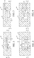
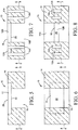
- Figs. 1 and 2 are elevation and plan section views, respectively, illustrating one example a new fluid flow structure 10.
- structure 10 includes a micro device 12 molded into in a monolithic body 14 of plastic or other moldable material.
- a molded body 14 is also referred to herein as a molding 14.
- Micro device 12 for example, could be an electronic device, a mechanical device, or a microelectromechanical system (MEMS) device.
- a channel or other suitable fluid flow path 16 is molded into body 14 in contact with micro device 12 so that fluid in channel 16 can flow directly into or onto device 12 (or both).
- channel 16 is connected to fluid flow passages 18 in micro device 12 and exposed to exterior surface 20 of micro device 12.
- flow path 16 in molding 14 allows air or other fluid to flow along an exterior surface 20 of micro device 12, for instance to cool device 12.
- signal traces or other conductors 22 connected to device 12 at electrical terminals 24 are molded into molding 14.
- micro device 12 is molded into body 14 with an exposed surface 26 opposite channel 16.
- micro devices 12A and 12B are molded into body 14 with fluid flow channels 16A and 16B. In this example, flow channels 16A contact the edges of outboard devices 12A while flow channel 16B contacts the bottom of inboard device 12B.
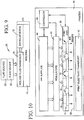
- Fig. 9 is a block diagram illustrating a system 28 implementing a new fluid flow structure 10 such as one of the flow structures 10 shown in Figs. 1-8 .
- system 28 includes a fluid source 30 operatively connected to a fluid mover 32 configured to move fluid to flow path 16 in structure 10.
- a fluid source 30 might include, for example, the atmosphere as a source of air to cool an electronic micro device 12 or a printing fluid supply for a printhead micro device 12.
- Fluid mover 32 represents a pump, a fan, gravity or any other suitable mechanism for moving fluid from source 30 to flow structure 10.
- Fig. 10 is a block diagram illustrating an inkjet printer 34 implementing one example of a new fluid flow structure 10 in a substrate wide print bar 36.
- printer 34 includes print bar 36 spanning the width of a print substrate 38, flow regulators 40 associated with print bar 36, a substrate transport mechanism 42, ink or other printing fluid supplies 44, and a printer controller 46.
- Controller 46 represents the programming, processor(s) and associated memories, and the electronic circuitry and components needed to control the operative elements of a printer 10.
- Print bar 36 includes an arrangement of printheads 37 for dispensing printing fluid on to a sheet or continuous web of paper or other print substrate 38.
- each printhead 37 includes one or more printhead dies in a molding with channels 16 to feed printing fluid directly to the die(s).
- Each printhead die receives printing fluid through a flow path from supplies 44 into and through flow regulators 40 and channels 16 in print bar 36.
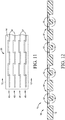
- Figs. 11-16 illustrate an inkjet print bar 36 implementing one example of a new fluid flow structure 10, such as might be used in printer 34 shown in Fig. 10 .
- printheads 37 are embedded in an elongated, monolithic molding 14 and arranged generally end to end in rows 48 in a staggered configuration in which the printheads in each row overlap another printhead in that row.
- four rows 48 of staggered printheads 37 are shown, for printing four different colors for example, other suitable configurations are possible.
- each printhead 37 includes a pair of printhead dies 12 each with two rows of ejection chambers 50 and corresponding orifices 52 through which printing fluid is ejected from chambers 50.
- Each channel 16 in molding 14 supplies printing fluid to one printhead die 12.
- Other suitable configurations for printhead 37 are possible.
- more or fewer printhead dies 12 may be used with more or fewer ejection chambers 50 and channels 16.
- Printing fluid flows into each ejection chamber 50 from a manifold 54 extending lengthwise along each die 12 between the two rows of ejection chambers 50. Printing fluid feeds into manifold 54 through multiple ports 56 that are connected to a printing fluid supply channel 16 at die surface 20.
- Printing fluid supply channel 16 is substantially wider than printing fluid ports 56, as shown, to carry printing fluid from larger, loosely spaced passages in the flow regulator or other parts that carry printing fluid into print bar 36 to the smaller, tightly spaced printing fluid ports 56 in printhead die 12.
- printing fluid supply channels 16 can help reduce or even eliminate the need for a discrete "fan-out" and other fluid routing structures necessary in some conventional printheads.
- exposing a substantial area of printhead die surface 20 directly to channel 16, as shown, allows printing fluid in channel 16 to help cool die 12 during printing.
- the idealized representation of a printhead die 12 in Figs. 11-15 depicts three layers 58, 60, 62 for convenience only to clearly show ejection chambers 50, orifices 52, manifold 54, and ports 56.
- An actual inkjet printhead die 12 is a typically complex integrated circuit (IC) structure formed on a silicon substrate 58 with layers and elements not shown in Figs. 11-15 .
- IC integrated circuit
- a thermal ejector element or a piezoelectric ejector element formed on substrate 58 at each ejection chamber 50 is actuated to eject drops or streams of ink or other printing fluid from orifices 52.
- a molded flow structure 10 enables the use of long, narrow and very thin printhead dies 12. For example, it has been shown that a 100 ⁇ m thick printhead die 12 that is about 26mm long and 500 ⁇ m wide can be molded into a 500 ⁇ m thick body 14 to replace a conventional 500 ⁇ m thick silicon printhead die. Not only is it cheaper and easier to mold channels 16 into body 14 compared to forming the feed channels in a silicon substrate, but it is also cheaper and easier to form printing fluid ports 56 in a thinner die 12. For example, ports 56 in a 100 ⁇ m thick printhead die 12 may be formed by dry etching and other suitable micromachining techniques not practical for thicker substrates.
- Micromachining a high density array of straight or slightly tapered through ports 56 in a thin silicon, glass or other substrate 58 rather than forming conventional slots leaves a stronger substrate while still providing adequate printing fluid flow.
- Tapered ports 56 help move air bubbles away from manifold 54 and ejection chambers 50 formed, for example, in a monolithic or multilayered orifice plate 60/62 applied to substrate 58. It is expected that current die handling equipment and micro device molding tools and techniques can adapted to mold dies 12 as thin as 50 ⁇ m, with a length/width ratio up to 150, and to mold channels 16 as narrow as 30 ⁇ m. And, the molding 14 provides an effective but inexpensive structure in which multiple rows of such die slivers can be supported in a single, monolithic body.
- Figs. 17-21 illustrate one example process for making a new printhead fluid flow structure 10.
- Fig. 22 is a flow diagram of the process illustrated in Figs. 17-21 .
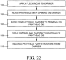
- a flex circuit 64 with conductive traces 22 and protective layer 66 is laminated on to a carrier 68 with a thermal release tape 70, or otherwise applied to carrier 68 (step 102 in Fig. 22 ).
- printhead die 12 is placed orifice side down in opening 72 on carrier 68 (step 104 in Fig. 22 ) and conductor 22 is bonded to an electrical terminal 24 on die 12 (step 106 in Fig. 22 ).
- Fig. 17 illustrates. 17-21 .
- a flex circuit 64 with conductive traces 22 and protective layer 66 is laminated on to a carrier 68 with a thermal release tape 70, or otherwise applied to carrier 68 (step 102 in Fig. 22 ).
- Figs. 18 and 19 printhead die 12 is placed orifice side down in opening 72 on carrier 68 (step
- a molding tool 74 forms channel 16 in a molding 14 around printhead die 12 (step 108 in Fig. 22 ).
- a tapered channel 16 may be desirable in some applications to facilitate the release of molding tool 74 or to increase fan-out (or both).
- printhead flow structure 10 is released from carrier 68 (step 110 in Fig. 22 ) to form the completed part shown in Fig. 21 in which conductor 22 is covered by layer 66 and surrounded by molding 14.
- channels 16 are molded into body 14. In other fabrication processes, it may be desirable to form channels 16 after molding body 14 around printhead die 12.
- FIGs. 23-28 illustrate one example wafer level process for making print bars 36.
- printheads 37 are placed on a glass or other suitable carrier wafer 68 in a pattern of multiple print bars.
- Printheads 37 usually will be placed on to carrier 68 after first applying or forming a pattern of conductors 22 and die openings 72 as described above with reference to Fig. 17 and step 102 in Fig. 22 .
- FIG. 23 In the example shown in Fig. 23 , five sets of dies 78 each having four rows of printheads 37 are laid out on carrier wafer 66 to form five print bars.
- five die sets 78 may be laid out on a single 270mm x 90mm carrier wafer 66 as shown in Fig. 23 .
- an array of conductors 22 extend to bond pads 23 near the edge of each row of printheads 37. Conductors 22 and bond pads 23 are more clearly visible in the detail of Fig. 28 . (Conductive signal traces to individual ejection chambers or groups of ejection chambers, such as conductors 22 in Fig. 21 , are omitted to not obscure other structural features.)
- Fig. 24 is a close-up section view of one set of four rows of printheads 37 taken along the line 24-24 in Fig. 23 . Cross hatching is omitted for clarity.
- Figs. 23 and 24 show the in-process wafer structure after the completion of steps 102-112 in Fig. 23 .
- Fig. 25 shows the section of Fig. 24 after molding step 114 in Fig. 23 in which body 14 with channels 16 is molded around printhead dies 12.
- Individual print bar strips 78 are separated in Fig. 26 and released from carrier 68 in Fig. 27 to form five individual print bars 36 (step 116 in Fig. 23 ). While any suitable molding technology may be used, testing suggests that wafer level molding tools and techniques currently used for semiconductor device packaging may be adapted cost effectively to the fabrication of printhead die fluid flow structures 10 such as those shown in Figs. 21 and 27 .
- a stiffer molding 14 may be used where a rigid (or at least less flexible) print bar 36 is desired to hold printhead dies 12.
- a less stiff molding 14 may be used where a flexible print bar 36 is desired, for example where another support structure holds the print bar rigidly in a single plane or where a nonplanar print bar configuration is desired.
- molded body 14 usually will be molded as a monolithic part, body 14 could be molded as more than one part.
- Figs. 29-31 illustrate other examples of a new fluid flow structure 10 for a printhead die 12.
- channels 16 are molded in body 14 along each side of printhead die 12, for example using a transfer molding process such as that described above with reference to Figs. 17-21 .
- Printing fluid flows from channels 16 through ports 56 laterally into each ejection chamber 50 directly from channels 16.
- orifice plate 62 is applied after molding body 14 to close channels 16.
- a cover 80 is formed over orifice plate 62 to close channels 16.
- an integrated cover 80 molded into body 14 could also be used.
Landscapes
- Engineering & Computer Science (AREA)
- Manufacturing & Machinery (AREA)
- Particle Formation And Scattering Control In Inkjet Printers (AREA)
- Ink Jet (AREA)
- Impression-Transfer Materials And Handling Thereof (AREA)
- Pens And Brushes (AREA)
Description
- Each printhead die in an inkjet pen or print bar includes tiny channels that carry ink to the ejection chambers. Ink is distributed from the ink supply to the die channels through passages in a structure that supports the printhead die(s) on the pen or print bar. It may be desirable to shrink the size of each printhead die, for example to reduce the cost of the die and, accordingly, to reduce the cost of the pen or print bar. The use of smaller dies, however, can require changes to the larger structures that support the dies, including the passages that distribute ink to the dies.
-
EP 1095773 A1 discloses an inkjet printhead. A carrier formed on molded plastic may contain a fluid ejecting substrate including a fluid channel in fluidic communication with an ink chamber. - JPS 61-125852 discloses an inkjet head having a structure of an orifice plate provided with an ink discharge port.
-
US 4,881,318 discloses a method of manufacturing a liquid jet recording head. -
US 2012/0212540 A1 discloses a printhead assembly and a fluidic connection of a die. -
- Each pair of
Figs. 1/2, 3/4 ,5/6, and 7/8 illustrate one example of a new molded fluid flow structure in which a micro device is embedded in a molding with a fluid flow path directly to the device. -
Fig. 9 is a block diagram illustrating a fluid flow system implementing a new fluid flow structure such as one of the examples shown inFigs. 1-8 . -
Fig. 10 is a block diagram illustrating an inkjet printer implementing one example of a new fluid flow structure for the printheads in a substrate wide print bar. -
Figs. 11-16 illustrate an inkjet print bar implementing one example of a new fluid flow structure for a printhead die, such as might be used in the printer ofFig. 10 . -
Figs. 17-21 are section views illustrating one example of a process for making a new printhead die fluid flow structure. -
Fig. 22 is a flow diagram of the process shown inFigs. 17-21 . -
Figs. 23-27 are perspective views illustrating one example of a wafer level process for making a new inkjet print bar such as the print bar shown inFigs. 11-16 . -
Fig. 28 is a detail fromFig. 23 . -
Figs. 29- 31 illustrate other examples of a new fluid flow structure for a printhead die. - The same part numbers designate the same or similar parts throughout the figures. The figures are not necessarily to scale. The relative size of some parts is exaggerated to more clearly illustrate the example shown.
- Inkjet printers that utilize a substrate wide print bar assembly have been developed to help increase printing speeds and reduce printing costs. Conventional substrate wide print bar assemblies include multiple parts that carry printing fluid from the printing fluid supplies to the small printhead dies from which the printing fluid is ejected on to the paper or other print substrate. While reducing the size and spacing of the printhead dies continues to be important for reducing cost, channeling printing fluid from the larger supply components to ever smaller, more tightly spaced dies requires complex flow structures and fabrication processes that can actually increase cost.
- A new fluid flow structure has been developed to enable the use of smaller printhead dies and more compact die circuitry to help reduce cost in substrate wide inkjet printers. A print bar implementing one example of the new structure includes multiple printhead dies molded into an elongated, monolithic body of moldable material. Printing fluid channels molded into the body carry printing fluid directly to printing fluid flow passages in each die. The molding in effect grows the size of each die for making external fluid connections and for attaching the dies to other structures, thus enabling the use of smaller dies. The printhead dies and printing fluid channels can be molded at the wafer level to form a new, composite printhead wafer with built-in printing fluid channels, eliminating the need to form the printing fluid channels in a silicon substrate and enabling the use of thinner dies.
- The new fluid flow structure is not limited to print bars or other types of printhead structures for inkjet printing, but may be implemented in other devices and for other fluid flow applications. Thus, in one example, the new structure includes a micro device embedded in a molding having a channel or other path for fluid to flow directly into or onto the device. The micro device, for example, could be an electronic device, a mechanical device, or a microelectromechanical system (MEMS) device. The fluid flow, for example, could be a cooling fluid flow into or onto the micro device or fluid flow into a printhead die or other fluid dispensing micro device.
- These and other examples shown in the figures and described below illustrate but do not limit the invention, which is defined in the Claims following this Description.
- As used in this document, a "micro device" means a device having one or more exterior dimensions less than or equal to 30mm; "thin" means a thickness less than or equal to 650µm; a "sliver" means a thin micro device having a ratio of length to width (L/W) of at least three; a "printhead" and a "printhead die" mean that part of an inkjet printer or other inkjet type dispenser that dispenses fluid from one or more openings. A printhead includes one or more printhead dies. "Printhead" and "printhead die" are not limited to printing with ink and other printing fluids but also include inkjet type dispensing of other fluids and/or for uses other than printing.
-
Figs. 1 and 2 are elevation and plan section views, respectively, illustrating one example a newfluid flow structure 10. Referring toFigs. 1 and 2 ,structure 10 includes amicro device 12 molded into in amonolithic body 14 of plastic or other moldable material. A moldedbody 14 is also referred to herein as amolding 14.Micro device 12, for example, could be an electronic device, a mechanical device, or a microelectromechanical system (MEMS) device. A channel or other suitablefluid flow path 16 is molded intobody 14 in contact withmicro device 12 so that fluid inchannel 16 can flow directly into or onto device 12 (or both). In this example,channel 16 is connected tofluid flow passages 18 inmicro device 12 and exposed toexterior surface 20 ofmicro device 12. - In another example, shown in
Figs. 3 and 4 ,flow path 16 inmolding 14 allows air or other fluid to flow along anexterior surface 20 ofmicro device 12, for instance tocool device 12. Also, in this example, signal traces orother conductors 22 connected todevice 12 atelectrical terminals 24 are molded intomolding 14. In another example, shown inFigs. 5 and 6 ,micro device 12 is molded intobody 14 with an exposedsurface 26opposite channel 16. In another example, shown inFigs. 7 and 8 ,micro devices body 14 withfluid flow channels flow channels 16A contact the edges ofoutboard devices 12A whileflow channel 16B contacts the bottom ofinboard device 12B. -
Fig. 9 is a block diagram illustrating asystem 28 implementing a newfluid flow structure 10 such as one of theflow structures 10 shown inFigs. 1-8 . Referring toFig. 9 ,system 28 includes afluid source 30 operatively connected to afluid mover 32 configured to move fluid toflow path 16 instructure 10. Afluid source 30 might include, for example, the atmosphere as a source of air to cool an electronicmicro device 12 or a printing fluid supply for aprinthead micro device 12.Fluid mover 32 represents a pump, a fan, gravity or any other suitable mechanism for moving fluid fromsource 30 toflow structure 10. -
Fig. 10 is a block diagram illustrating aninkjet printer 34 implementing one example of a newfluid flow structure 10 in a substratewide print bar 36. Referring toFig. 10 ,printer 34 includesprint bar 36 spanning the width of aprint substrate 38,flow regulators 40 associated withprint bar 36, asubstrate transport mechanism 42, ink or otherprinting fluid supplies 44, and aprinter controller 46.Controller 46 represents the programming, processor(s) and associated memories, and the electronic circuitry and components needed to control the operative elements of aprinter 10.Print bar 36 includes an arrangement ofprintheads 37 for dispensing printing fluid on to a sheet or continuous web of paper orother print substrate 38. As described in detail below, eachprinthead 37 includes one or more printhead dies in a molding withchannels 16 to feed printing fluid directly to the die(s). Each printhead die receives printing fluid through a flow path fromsupplies 44 into and throughflow regulators 40 andchannels 16 inprint bar 36. -
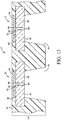
Figs. 11-16 illustrate aninkjet print bar 36 implementing one example of a newfluid flow structure 10, such as might be used inprinter 34 shown inFig. 10 . Referring first to the plan view ofFig. 11 ,printheads 37 are embedded in an elongated,monolithic molding 14 and arranged generally end to end inrows 48 in a staggered configuration in which the printheads in each row overlap another printhead in that row. Although fourrows 48 of staggeredprintheads 37 are shown, for printing four different colors for example, other suitable configurations are possible. -
Fig. 12 is a section view taken along the line 12-12 inFig. 11 .Figs. 13-15 are detail views fromFig. 12 , andFig. 16 is a plan view diagram showing the layout of some of the features of printhead dieflow structure 10 inFigs. 12-14 . Referring now toFigs. 11-15 , in the example shown, eachprinthead 37 includes a pair of printhead dies 12 each with two rows ofejection chambers 50 andcorresponding orifices 52 through which printing fluid is ejected fromchambers 50. Eachchannel 16 inmolding 14 supplies printing fluid to one printhead die 12. Other suitable configurations forprinthead 37 are possible. For example, more or fewer printhead dies 12 may be used with more orfewer ejection chambers 50 andchannels 16. (Althoughprint bar 36 andprintheads 37 face up inFigs. 12-15 ,print bar 36 andprintheads 37 usually face down when installed in a printer, as depicted in the block diagram ofFig. 10 .) - Printing fluid flows into each
ejection chamber 50 from a manifold 54 extending lengthwise along each die 12 between the two rows ofejection chambers 50. Printing fluid feeds intomanifold 54 throughmultiple ports 56 that are connected to a printingfluid supply channel 16 atdie surface 20. Printingfluid supply channel 16 is substantially wider than printingfluid ports 56, as shown, to carry printing fluid from larger, loosely spaced passages in the flow regulator or other parts that carry printing fluid intoprint bar 36 to the smaller, tightly spacedprinting fluid ports 56 in printhead die 12. Thus, printingfluid supply channels 16 can help reduce or even eliminate the need for a discrete "fan-out" and other fluid routing structures necessary in some conventional printheads. In addition, exposing a substantial area of printhead diesurface 20 directly tochannel 16, as shown, allows printing fluid inchannel 16 to help cool die 12 during printing. - The idealized representation of a
printhead die 12 inFigs. 11-15 depicts threelayers ejection chambers 50,orifices 52,manifold 54, andports 56. An actual inkjet printhead die 12 is a typically complex integrated circuit (IC) structure formed on asilicon substrate 58 with layers and elements not shown inFigs. 11-15 . For example, a thermal ejector element or a piezoelectric ejector element formed onsubstrate 58 at eachejection chamber 50 is actuated to eject drops or streams of ink or other printing fluid fromorifices 52. - A molded
flow structure 10 enables the use of long, narrow and very thin printhead dies 12. For example, it has been shown that a 100µm thick printhead die 12 that is about 26mm long and 500µm wide can be molded into a 500µmthick body 14 to replace a conventional 500µm thick silicon printhead die. Not only is it cheaper and easier to moldchannels 16 intobody 14 compared to forming the feed channels in a silicon substrate, but it is also cheaper and easier to form printingfluid ports 56 in athinner die 12. For example,ports 56 in a 100µm thick printhead die 12 may be formed by dry etching and other suitable micromachining techniques not practical for thicker substrates. Micromachining a high density array of straight or slightly tapered throughports 56 in a thin silicon, glass orother substrate 58 rather than forming conventional slots leaves a stronger substrate while still providing adequate printing fluid flow.Tapered ports 56 help move air bubbles away frommanifold 54 andejection chambers 50 formed, for example, in a monolithic ormultilayered orifice plate 60/62 applied tosubstrate 58. It is expected that current die handling equipment and micro device molding tools and techniques can adapted to mold dies 12 as thin as 50µm, with a length/width ratio up to 150, and to moldchannels 16 as narrow as 30µm. And, themolding 14 provides an effective but inexpensive structure in which multiple rows of such die slivers can be supported in a single, monolithic body. -
Figs. 17-21 illustrate one example process for making a new printheadfluid flow structure 10.Fig. 22 is a flow diagram of the process illustrated inFigs. 17-21 . Referring first toFig. 17 , aflex circuit 64 withconductive traces 22 andprotective layer 66 is laminated on to acarrier 68 with athermal release tape 70, or otherwise applied to carrier 68 (step 102 inFig. 22 ). As shown inFigs. 18 and 19 , printhead die 12 is placed orifice side down in opening 72 on carrier 68 (step 104 inFig. 22 ) andconductor 22 is bonded to anelectrical terminal 24 on die 12 (step 106 inFig. 22 ). InFig. 20 , amolding tool 74 forms channel 16 in amolding 14 around printhead die 12 (step 108 inFig. 22 ). A taperedchannel 16 may be desirable in some applications to facilitate the release ofmolding tool 74 or to increase fan-out (or both). After molding,printhead flow structure 10 is released from carrier 68 (step 110 inFig. 22 ) to form the completed part shown inFig. 21 in whichconductor 22 is covered bylayer 66 and surrounded bymolding 14. In a transfer molding process such as that shown inFig. 20 ,channels 16 are molded intobody 14. In other fabrication processes, it may be desirable to formchannels 16 after moldingbody 14 around printhead die 12. - While the molding of a single printhead die 12 and
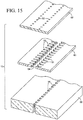
channel 16 is shown inFigs. 17-21 , multiple printhead dies and printing fluid channels can be molded simultaneously at the wafer level.Figs. 23-28 illustrate one example wafer level process for making print bars 36. Referring toFig. 23 ,printheads 37 are placed on a glass or othersuitable carrier wafer 68 in a pattern of multiple print bars. (Although a "wafer" is sometimes used to denote a round substrate while a "panel" is used to denote a rectangular substrate, a "wafer" as used in this document includes any shape substrate.)Printheads 37 usually will be placed on tocarrier 68 after first applying or forming a pattern ofconductors 22 and dieopenings 72 as described above with reference toFig. 17 andstep 102 inFig. 22 . - In the example shown in
Fig. 23 , five sets of dies 78 each having four rows ofprintheads 37 are laid out oncarrier wafer 66 to form five print bars. A substrate wide print bar for printing on Letter or A4 size substrates with four rows ofprintheads 37, for example, is about 230mm long and 16mm wide. Thus, five die sets 78 may be laid out on a single 270mm x90mm carrier wafer 66 as shown inFig. 23 . Again, in the example shown, an array ofconductors 22 extend to bondpads 23 near the edge of each row ofprintheads 37.Conductors 22 andbond pads 23 are more clearly visible in the detail ofFig. 28 . (Conductive signal traces to individual ejection chambers or groups of ejection chambers, such asconductors 22 inFig. 21 , are omitted to not obscure other structural features.) -
Fig. 24 is a close-up section view of one set of four rows ofprintheads 37 taken along the line 24-24 inFig. 23 . Cross hatching is omitted for clarity.Figs. 23 and24 show the in-process wafer structure after the completion of steps 102-112 inFig. 23 .Fig. 25 shows the section ofFig. 24 after molding step 114 inFig. 23 in whichbody 14 withchannels 16 is molded around printhead dies 12. Individual print bar strips 78 are separated inFig. 26 and released fromcarrier 68 inFig. 27 to form five individual print bars 36 (step 116 inFig. 23 ). While any suitable molding technology may be used, testing suggests that wafer level molding tools and techniques currently used for semiconductor device packaging may be adapted cost effectively to the fabrication of printhead diefluid flow structures 10 such as those shown inFigs. 21 and27 . - A
stiffer molding 14 may be used where a rigid (or at least less flexible)print bar 36 is desired to hold printhead dies 12. A lessstiff molding 14 may be used where aflexible print bar 36 is desired, for example where another support structure holds the print bar rigidly in a single plane or where a nonplanar print bar configuration is desired. Also, although it is expected that moldedbody 14 usually will be molded as a monolithic part,body 14 could be molded as more than one part. -
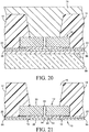
Figs. 29-31 illustrate other examples of a newfluid flow structure 10 for aprinthead die 12. In these examples,channels 16 are molded inbody 14 along each side of printhead die 12, for example using a transfer molding process such as that described above with reference toFigs. 17-21 . Printing fluid flows fromchannels 16 throughports 56 laterally into eachejection chamber 50 directly fromchannels 16. In the example ofFig. 30 ,orifice plate 62 is applied after moldingbody 14 to closechannels 16. In the example ofFig. 31 , acover 80 is formed overorifice plate 62 to closechannels 16. Although adiscrete cover 80 partially definingchannels 16 is shown, anintegrated cover 80 molded intobody 14 could also be used. - As noted at the beginning of this Description, the examples shown in the figures and described above illustrate but do not limit the invention. Other examples are possible. Therefore, the foregoing description should not be construed to limit the scope of the invention, which is defined in the following claims.
Claims (10)
- A structure (10), comprising:
a printhead die (12) molded into a monolithic body (14) of plastic or other moldable material, wherein the monolithic body (14) has a channel (16) in contact with the printhead die (12) so that fluid may pass directly to the printhead die (12),
wherein the printhead die (12) includes:multiple holes (56) connected to the channel (16) such that printing fluid can flow from the channel (16) directly into the holes (56);a manifold (54) connected to the holes (56) such that printing fluid can flow from the holes (56) directly into the manifold (54); andmultiple ejection chambers (50) connected to the manifold (54) such that printing fluid can flow from the manifold (54) into the ejection chambers (50),characterized in that:each hole (56) is tapered from a broader part at the channel (16) to a narrower part at the manifold (54); andthe channel (16) is molded into the body (14) and tapered from a broader part away from the holes (56) to a narrower part at the holes (56). - The structure (10) of Claim 1, wherein the printhead die (12) is a thin die, and wherein the thin die has a thickness less than or equal to 650µm.
- The structure (10) of Claim 2, wherein the thin die (12) is a die sliver, and wherein the printhead die sliver has a ratio of length to width (L/W) of at least three.
- The structure of any one of Claims 1 to 3, wherein:the printhead die (12) includes a front with orifices (52) through which fluid may be dispensed from the printhead die (12), a back opposite the front, and sides between the front and back; andthe channel (16) is located at the back side of the printhead die (12).
- The structure (10) of any one of Claims 1 to 4, wherein the monolithic body (14) is molded around the printhead die (12).
- The structure (10) of any one of Claims 1 to 5, wherein the printhead die (12) includes an electrical terminal and the structure (10) further comprises conductors connected to the terminals, the monolithic body (14) molded around the conductors and the terminals.
- The structure (10) of any one of Claims 1 to 6, wherein the printhead die (12) includes a front with orifices (52) through which fluid may be dispensed from the printhead die (12), a back opposite the front, and sides between the front and back, and wherein the monolithic body (14) is partially encapsulating the printhead die (12) such that the back of the printhead die (12) is partially covered by the monolithic body (14) and the sides between the front and back are completely covered by the monolithic body (14).
- The structure (10) of any one of Claims 1 to 7, wherein the channel (16) is molded into the molding.
- A print head, comprising one or more structures of any one of Claims 1 to 8.
- An inkjet pen, comprising one or more print heads of Claim 9.
Priority Applications (4)
| Application Number | Priority Date | Filing Date | Title |
|---|---|---|---|
| PL17200873T PL3296113T3 (en) | 2013-02-28 | 2013-02-28 | Molded print bar |
| EP17200873.2A EP3296113B1 (en) | 2013-02-28 | 2013-02-28 | Molded print bar |
| ES17200873T ES2747823T3 (en) | 2013-02-28 | 2013-02-28 | Molded print bar |
| HUE17200873A HUE045188T2 (en) | 2013-02-28 | 2013-02-28 | Molded print bar |
Applications Claiming Priority (3)
| Application Number | Priority Date | Filing Date | Title |
|---|---|---|---|
| EP13876635.7A EP2961614B1 (en) | 2013-02-28 | 2013-02-28 | Molded print bar |
| PCT/US2013/028216 WO2014133517A1 (en) | 2013-02-28 | 2013-02-28 | Molded print bar |
| EP17200873.2A EP3296113B1 (en) | 2013-02-28 | 2013-02-28 | Molded print bar |
Related Parent Applications (2)
| Application Number | Title | Priority Date | Filing Date |
|---|---|---|---|
| EP13876635.7A Division EP2961614B1 (en) | 2013-02-28 | 2013-02-28 | Molded print bar |
| EP13876635.7A Division-Into EP2961614B1 (en) | 2013-02-28 | 2013-02-28 | Molded print bar |
Publications (2)
| Publication Number | Publication Date |
|---|---|
| EP3296113A1 EP3296113A1 (en) | 2018-03-21 |
| EP3296113B1 true EP3296113B1 (en) | 2019-08-28 |
Family
ID=51428637
Family Applications (5)
| Application Number | Title | Priority Date | Filing Date |
|---|---|---|---|
| EP13876635.7A Active EP2961614B1 (en) | 2013-02-28 | 2013-02-28 | Molded print bar |
| EP20151711.7A Active EP3656570B1 (en) | 2013-02-28 | 2013-02-28 | Molded print bar |
| EP17200873.2A Active EP3296113B1 (en) | 2013-02-28 | 2013-02-28 | Molded print bar |
| EP13876407.1A Active EP2961609B1 (en) | 2013-02-28 | 2013-09-27 | Molded printhead |
| EP13876179.6A Active EP2825385B1 (en) | 2013-02-28 | 2013-11-05 | Molded printhead |
Family Applications Before (2)
| Application Number | Title | Priority Date | Filing Date |
|---|---|---|---|
| EP13876635.7A Active EP2961614B1 (en) | 2013-02-28 | 2013-02-28 | Molded print bar |
| EP20151711.7A Active EP3656570B1 (en) | 2013-02-28 | 2013-02-28 | Molded print bar |
Family Applications After (2)
| Application Number | Title | Priority Date | Filing Date |
|---|---|---|---|
| EP13876407.1A Active EP2961609B1 (en) | 2013-02-28 | 2013-09-27 | Molded printhead |
| EP13876179.6A Active EP2825385B1 (en) | 2013-02-28 | 2013-11-05 | Molded printhead |
Country Status (12)
| Country | Link |
|---|---|
| US (9) | US9902162B2 (en) |
| EP (5) | EP2961614B1 (en) |
| JP (3) | JP6261623B2 (en) |
| KR (4) | KR102005466B1 (en) |
| CN (4) | CN107901609B (en) |
| BR (1) | BR112015020862B1 (en) |
| ES (1) | ES2747823T3 (en) |
| HU (1) | HUE045188T2 (en) |
| PL (1) | PL3296113T3 (en) |
| RU (2) | RU2633224C2 (en) |
| TW (4) | TWI531480B (en) |
| WO (4) | WO2014133517A1 (en) |
Families Citing this family (45)
| Publication number | Priority date | Publication date | Assignee | Title |
|---|---|---|---|---|
| US10821729B2 (en) | 2013-02-28 | 2020-11-03 | Hewlett-Packard Development Company, L.P. | Transfer molded fluid flow structure |
| BR112015020860B1 (en) * | 2013-02-28 | 2021-04-13 | Hewlett-Packard Development Company, L.P. | FLUID FLOW STRUCTURE AND SYSTEM WITH A MICRO DEVICE FLUID DISPENSER AND A MONOLITHIC MOLDING |
| RU2633224C2 (en) * | 2013-02-28 | 2017-10-11 | Хьюлетт-Паккард Дивелопмент Компани, Л.П. | Formated printing stands |
| US11426900B2 (en) | 2013-02-28 | 2022-08-30 | Hewlett-Packard Development Company, L.P. | Molding a fluid flow structure |
| US9724920B2 (en) * | 2013-03-20 | 2017-08-08 | Hewlett-Packard Development Company, L.P. | Molded die slivers with exposed front and back surfaces |
| WO2015041665A1 (en) | 2013-09-20 | 2015-03-26 | Hewlett-Packard Development Company, L.P. | Printbar and method of forming same |
| US9889664B2 (en) | 2013-09-20 | 2018-02-13 | Hewlett-Packard Development Company, L.P. | Molded printhead structure |
| US10160209B2 (en) | 2014-01-28 | 2018-12-25 | Hewlett-Packard Development Company, L.P. | Flexible carrier for fluid flow structure |
| WO2015116076A1 (en) | 2014-01-30 | 2015-08-06 | Hewlett-Packard Development Company, Lp | Printed circuit board fluid ejection apparatus |
| US9770909B2 (en) | 2014-01-30 | 2017-09-26 | Hewlett-Packard Development Company, L.P. | Printhead dies molded with nozzle health sensor |
| KR101492396B1 (en) | 2014-09-11 | 2015-02-13 | 주식회사 우심시스템 | Array type ink cartridge |
| EP3233500B1 (en) * | 2015-02-27 | 2021-12-01 | Hewlett-Packard Development Company, L.P. | Fluid ejection device with fluid feed holes |
| JP6643073B2 (en) * | 2015-06-29 | 2020-02-12 | 東芝テック株式会社 | Droplet dispensing device |
| US11051875B2 (en) | 2015-08-24 | 2021-07-06 | Medtronic Advanced Energy Llc | Multipurpose electrosurgical device |
| WO2017065725A1 (en) * | 2015-10-12 | 2017-04-20 | Hewlett-Packard Development Company, L.P. | Printhead |
| JP6659738B2 (en) * | 2015-10-12 | 2020-03-04 | ヒューレット−パッカード デベロップメント カンパニー エル.ピー.Hewlett‐Packard Development Company, L.P. | Print head |
| WO2017065772A1 (en) | 2015-10-15 | 2017-04-20 | Hewlett-Packard Development Company, L.P. | Print head interposers |
| WO2017069748A1 (en) * | 2015-10-21 | 2017-04-27 | Hewlett-Packard Development Company, L.P. | Printhead electrical interconnects |
| WO2017074302A1 (en) * | 2015-10-26 | 2017-05-04 | Hewlett-Packard Development Company, L.P. | Printheads and methods of fabricating a printhead |
| US10272684B2 (en) | 2015-12-30 | 2019-04-30 | Stmicroelectronics, Inc. | Support substrates for microfluidic die |
| CN108513550B (en) * | 2016-02-05 | 2020-10-23 | 惠普发展公司,有限责任合伙企业 | Print bar and printing system thereof |
| US10864719B2 (en) * | 2016-02-24 | 2020-12-15 | Hewlett-Packard Development Company, L.P. | Fluid ejection device including integrated circuit |
| JP6911170B2 (en) * | 2016-02-24 | 2021-07-28 | ヒューレット−パッカード デベロップメント カンパニー エル.ピー.Hewlett‐Packard Development Company, L.P. | Fluid discharge device including integrated circuits |
| US11383230B2 (en) | 2016-03-31 | 2022-07-12 | Hewlett-Packard Development Company, L.P. | Monolithic carrier structure including fluid routing for digital dispensing |
| WO2018084827A1 (en) * | 2016-11-01 | 2018-05-11 | Hewlett-Packard Development Company, L.P. | Fluid ejection device |
| TW201838829A (en) * | 2017-02-06 | 2018-11-01 | 愛爾蘭商滿捷特科技公司 | Inkjet printhead for full color pagewide printing |
| US11325125B2 (en) | 2017-04-23 | 2022-05-10 | Hewlett-Packard Development Company, L.P. | Particle separation |
| US11097537B2 (en) | 2017-04-24 | 2021-08-24 | Hewlett-Packard Development Company, L.P. | Fluid ejection die molded into molded body |
| CN110461575B (en) * | 2017-05-01 | 2021-10-01 | 惠普发展公司,有限责任合伙企业 | Method for forming mold sheet and fluid ejection apparatus |
| JP6947550B2 (en) * | 2017-06-27 | 2021-10-13 | 株式会社ジャパンディスプレイ | Display device |
| US11211742B2 (en) * | 2017-07-24 | 2021-12-28 | Molex, Llc | Cable connector |
| JP7053786B2 (en) * | 2017-07-26 | 2022-04-12 | ヒューレット-パッカード デベロップメント カンパニー エル.ピー. | Die contact formation |
| EP3609712B1 (en) * | 2017-07-31 | 2023-11-29 | Hewlett-Packard Development Company, L.P. | Fluidic ejection devices with enclosed cross-channels |
| CN110891793B (en) | 2017-07-31 | 2021-04-09 | 惠普发展公司,有限责任合伙企业 | Fluid ejection die with enclosed lateral channels |
| CN110154544B (en) * | 2018-02-12 | 2020-11-24 | 海德堡印刷机械股份公司 | Print bar for ink jet |
| CN113272146B (en) * | 2019-01-09 | 2022-08-05 | 惠普发展公司,有限责任合伙企业 | Fluid feed hole port size |
| PT3710260T (en) | 2019-02-06 | 2021-08-19 | Hewlett Packard Development Co | Die for a printhead |
| WO2020162911A1 (en) * | 2019-02-06 | 2020-08-13 | Hewlett-Packard Development Company, L.P. | Die for a printhead |
| MX2021008855A (en) | 2019-02-06 | 2021-09-08 | Hewlett Packard Development Co | Die for a printhead. |
| WO2020162928A1 (en) | 2019-02-06 | 2020-08-13 | Hewlett-Packard Development Company, L.P. | Fluid ejection devices including electrical interconnect elements for fluid ejection dies |
| WO2020222736A1 (en) | 2019-04-29 | 2020-11-05 | Hewlett-Packard Development Company, L.P. | Fluid ejection device with break(s) in cover layer |
| WO2020263234A1 (en) * | 2019-06-25 | 2020-12-30 | Hewlett-Packard Development Company, L.P. | Molded structures with channels |
| WO2020263236A1 (en) * | 2019-06-25 | 2020-12-30 | Hewlett-Packard Development Company, L.P. | Molded structures with channels |
| TR202011480A2 (en) * | 2020-07-20 | 2022-02-21 | Hacettepe Ueniversitesi Rektoerluek | PRINTER DEVICE WITH AUTOMATIC PRINTING DEVICE FOR FLEXIBLE CIRCUIT APPLICATIONS |
| WO2023140856A1 (en) * | 2022-01-21 | 2023-07-27 | Hewlett-Packard Development Company, L.P. | Polymer based conductive paths for fluidic dies |
Family Cites Families (255)
| Publication number | Priority date | Publication date | Assignee | Title |
|---|---|---|---|---|
| US4224627A (en) | 1979-06-28 | 1980-09-23 | International Business Machines Corporation | Seal glass for nozzle assemblies of an ink jet printer |
| JPS58112754A (en) | 1981-12-26 | 1983-07-05 | Konishiroku Photo Ind Co Ltd | Recording head for ink jet recorder |
| US4460537A (en) | 1982-07-26 | 1984-07-17 | Motorola, Inc. | Slot transfer molding apparatus and methods |
| US4633274A (en) | 1984-03-30 | 1986-12-30 | Canon Kabushiki Kaisha | Liquid ejection recording apparatus |
| US4881318A (en) * | 1984-06-11 | 1989-11-21 | Canon Kabushiki Kaisha | Method of manufacturing a liquid jet recording head |
| JPH064325B2 (en) | 1984-06-11 | 1994-01-19 | キヤノン株式会社 | Liquid jet head |
| JPS61125852A (en) | 1984-11-22 | 1986-06-13 | Canon Inc | Ink jet recording head |
| JPS62240562A (en) | 1986-04-14 | 1987-10-21 | Matsushita Electric Works Ltd | Preparation of wire guide for dot printer |
| US4973622A (en) * | 1989-03-27 | 1990-11-27 | Ppg Industries, Inc. | Vinyl chloride-olefin copolymers having good color stability and flexibility for container coatings |
| US5016023A (en) | 1989-10-06 | 1991-05-14 | Hewlett-Packard Company | Large expandable array thermal ink jet pen and method of manufacturing same |
| US5124717A (en) | 1990-12-06 | 1992-06-23 | Xerox Corporation | Ink jet printhead having integral filter |
| AU657930B2 (en) | 1991-01-30 | 1995-03-30 | Canon Kabushiki Kaisha | Nozzle structures for bubblejet print devices |
| US5160945A (en) | 1991-05-10 | 1992-11-03 | Xerox Corporation | Pagewidth thermal ink jet printhead |
| JP3088849B2 (en) | 1992-06-30 | 2000-09-18 | 株式会社リコー | Inkjet recording head |
| US5387314A (en) | 1993-01-25 | 1995-02-07 | Hewlett-Packard Company | Fabrication of ink fill slots in thermal ink-jet printheads utilizing chemical micromachining |
| JPH06226977A (en) | 1993-02-01 | 1994-08-16 | Ricoh Co Ltd | Ink jet head |
| JP3444998B2 (en) | 1993-12-22 | 2003-09-08 | キヤノン株式会社 | Liquid jet head |
| US5565900A (en) | 1994-02-04 | 1996-10-15 | Hewlett-Packard Company | Unit print head assembly for ink-jet printing |
| JP3268937B2 (en) * | 1994-04-14 | 2002-03-25 | キヤノン株式会社 | Substrate for inkjet recording head and head using the same |
| US5538586A (en) * | 1994-10-04 | 1996-07-23 | Hewlett-Packard Company | Adhesiveless encapsulation of tab circuit traces for ink-jet pen |
| JP3459703B2 (en) | 1995-06-20 | 2003-10-27 | キヤノン株式会社 | Method of manufacturing inkjet head and inkjet head |
| JPH091812A (en) | 1995-06-21 | 1997-01-07 | Canon Inc | Manufacture of liquid ejection recording head and manufacturing machine |
| JPH0929970A (en) | 1995-07-19 | 1997-02-04 | Canon Inc | Ink jet recording head and manufacture thereof |
| EP0755793B1 (en) | 1995-07-26 | 2001-04-04 | Sony Corporation | Printer apparatus and method of production of same |
| US5745131A (en) * | 1995-08-03 | 1998-04-28 | Xerox Corporation | Gray scale ink jet printer |
| JP3402879B2 (en) | 1995-11-08 | 2003-05-06 | キヤノン株式会社 | INK JET HEAD, ITS MANUFACTURING METHOD, AND INK JET DEVICE |
| US6305790B1 (en) | 1996-02-07 | 2001-10-23 | Hewlett-Packard Company | Fully integrated thermal inkjet printhead having multiple ink feed holes per nozzle |
| EP0827834B1 (en) | 1996-03-22 | 2003-07-02 | Sony Corporation | Printer |
| US6257703B1 (en) * | 1996-07-31 | 2001-07-10 | Canon Kabushiki Kaisha | Ink jet recording head |
| US6281914B1 (en) | 1996-11-13 | 2001-08-28 | Brother Kogyo Kabushiki Kaisa | Ink jet-type printer device with printer head on circuit board |
| US5719605A (en) | 1996-11-20 | 1998-02-17 | Lexmark International, Inc. | Large array heater chips for thermal ink jet printheads |
| US6259463B1 (en) * | 1997-10-30 | 2001-07-10 | Hewlett-Packard Company | Multi-drop merge on media printing system |
| US5894108A (en) | 1997-02-11 | 1999-04-13 | National Semiconductor Corporation | Plastic package with exposed die |
| US6045214A (en) | 1997-03-28 | 2000-04-04 | Lexmark International, Inc. | Ink jet printer nozzle plate having improved flow feature design and method of making nozzle plates |
| US7708372B2 (en) | 1997-07-15 | 2010-05-04 | Silverbrook Research Pty Ltd | Inkjet nozzle with ink feed channels etched from back of wafer |
| US7527357B2 (en) | 1997-07-15 | 2009-05-05 | Silverbrook Research Pty Ltd | Inkjet nozzle array with individual feed channel for each nozzle |
| US6918654B2 (en) | 1997-07-15 | 2005-07-19 | Silverbrook Research Pty Ltd | Ink distribution assembly for an ink jet printhead |
| US5847725A (en) | 1997-07-28 | 1998-12-08 | Hewlett-Packard Company | Expansion relief for orifice plate of thermal ink jet print head |
| US6022482A (en) | 1997-08-04 | 2000-02-08 | Xerox Corporation | Monolithic ink jet printhead |
| JP3521706B2 (en) | 1997-09-24 | 2004-04-19 | 富士ゼロックス株式会社 | Ink jet recording head and method of manufacturing the same |
| US6508546B2 (en) | 1998-10-16 | 2003-01-21 | Silverbrook Research Pty Ltd | Ink supply arrangement for a portable ink jet printer |
| US6789878B2 (en) | 1997-10-28 | 2004-09-14 | Hewlett-Packard Development Company, L.P. | Fluid manifold for printhead assembly |
| US6123410A (en) | 1997-10-28 | 2000-09-26 | Hewlett-Packard Company | Scalable wide-array inkjet printhead and method for fabricating same |
| US6250738B1 (en) * | 1997-10-28 | 2001-06-26 | Hewlett-Packard Company | Inkjet printing apparatus with ink manifold |
| US6188414B1 (en) * | 1998-04-30 | 2001-02-13 | Hewlett-Packard Company | Inkjet printhead with preformed substrate |
| US6132028A (en) | 1998-05-14 | 2000-10-17 | Hewlett-Packard Company | Contoured orifice plate of thermal ink jet print head |
| US20020041308A1 (en) | 1998-08-05 | 2002-04-11 | Cleland Todd A. | Method of manufacturing an orifice plate having a plurality of slits |
| US6227651B1 (en) | 1998-09-25 | 2001-05-08 | Hewlett-Packard Company | Lead frame-mounted ink jet print head module |
| JP2000108360A (en) * | 1998-10-02 | 2000-04-18 | Sony Corp | Manufacture for print head |
| US6705705B2 (en) | 1998-12-17 | 2004-03-16 | Hewlett-Packard Development Company, L.P. | Substrate for fluid ejection devices |
| US6341845B1 (en) | 2000-08-25 | 2002-01-29 | Hewlett-Packard Company | Electrical connection for wide-array inkjet printhead assembly with hybrid carrier for printhead dies |
| US6464333B1 (en) * | 1998-12-17 | 2002-10-15 | Hewlett-Packard Company | Inkjet printhead assembly with hybrid carrier for printhead dies |
| US6745467B1 (en) | 1999-02-10 | 2004-06-08 | Canon Kabushiki Kaisha | Method of producing a liquid discharge head |
| US7182434B2 (en) | 1999-06-30 | 2007-02-27 | Silverbrook Research Pty Ltd | Inkjet printhead assembly having aligned printhead segments |
| US6254819B1 (en) | 1999-07-16 | 2001-07-03 | Eastman Kodak Company | Forming channel members for ink jet printheads |
| CN1286172A (en) * | 1999-08-25 | 2001-03-07 | 美商·惠普公司 | Method for mfg. film ink-jet print head |
| JP2001071490A (en) | 1999-09-02 | 2001-03-21 | Ricoh Co Ltd | Ink-jet recording device |
| US6616271B2 (en) | 1999-10-19 | 2003-09-09 | Silverbrook Research Pty Ltd | Adhesive-based ink jet print head assembly |
| US6190002B1 (en) | 1999-10-27 | 2001-02-20 | Lexmark International, Inc. | Ink jet pen |
| KR100657108B1 (en) * | 1999-10-29 | 2006-12-12 | 휴렛-팩커드 컴퍼니(델라웨어주법인) | Inkjet printhead having improved reliability |
| US6454955B1 (en) * | 1999-10-29 | 2002-09-24 | Hewlett-Packard Company | Electrical interconnect for an inkjet die |
| JP4533522B2 (en) * | 1999-10-29 | 2010-09-01 | ヒューレット・パッカード・カンパニー | Electrical interconnect for inkjet die |
| JP2001246748A (en) | 1999-12-27 | 2001-09-11 | Seiko Epson Corp | Ink-jet type recording head |
| US6679264B1 (en) | 2000-03-04 | 2004-01-20 | Emphasys Medical, Inc. | Methods and devices for use in performing pulmonary procedures |
| AUPQ605800A0 (en) * | 2000-03-06 | 2000-03-30 | Silverbrook Research Pty Ltd | Printehead assembly |
| US6560871B1 (en) * | 2000-03-21 | 2003-05-13 | Hewlett-Packard Development Company, L.P. | Semiconductor substrate having increased facture strength and method of forming the same |
| IT1320026B1 (en) * | 2000-04-10 | 2003-11-12 | Olivetti Lexikon Spa | MULTIPLE CHANNEL MONOLITHIC PRINT HEAD OF THE INK AND RELATED MANUFACTURING PROCESS. |
| US6379988B1 (en) * | 2000-05-16 | 2002-04-30 | Sandia Corporation | Pre-release plastic packaging of MEMS and IMEMS devices |
| US6786658B2 (en) | 2000-05-23 | 2004-09-07 | Silverbrook Research Pty. Ltd. | Printer for accommodating varying page thicknesses |
| JP4557386B2 (en) | 2000-07-10 | 2010-10-06 | キヤノン株式会社 | Manufacturing method for recording head substrate |
| IT1320599B1 (en) | 2000-08-23 | 2003-12-10 | Olivetti Lexikon Spa | MONOLITHIC PRINT HEAD WITH SELF-ALIGNED GROOVING AND RELATIVE MANUFACTURING PROCESS. |
| US6398348B1 (en) | 2000-09-05 | 2002-06-04 | Hewlett-Packard Company | Printing structure with insulator layer |
| US6896359B1 (en) * | 2000-09-06 | 2005-05-24 | Canon Kabushiki Kaisha | Ink jet recording head and method for manufacturing ink jet recording head |
| KR100677752B1 (en) | 2000-09-29 | 2007-02-05 | 삼성전자주식회사 | Ink-jet printer head and method of manufacturing thereof |
| US6402301B1 (en) * | 2000-10-27 | 2002-06-11 | Lexmark International, Inc | Ink jet printheads and methods therefor |
| US6291317B1 (en) | 2000-12-06 | 2001-09-18 | Xerox Corporation | Method for dicing of micro devices |
| US6554399B2 (en) | 2001-02-27 | 2003-04-29 | Hewlett-Packard Development Company, L.P. | Interconnected printhead die and carrier substrate system |
| JP2002291262A (en) | 2001-03-27 | 2002-10-04 | Hitachi Metals Ltd | Piezoelectric actuator and liquid eject head using it |
| US20020180825A1 (en) | 2001-06-01 | 2002-12-05 | Shen Buswell | Method of forming a fluid delivery slot |
| GB0113639D0 (en) | 2001-06-05 | 2001-07-25 | Xaar Technology Ltd | Nozzle plate for droplet deposition apparatus |
| US6561632B2 (en) | 2001-06-06 | 2003-05-13 | Hewlett-Packard Development Company, L.P. | Printhead with high nozzle packing density |
| JP2003011365A (en) | 2001-07-04 | 2003-01-15 | Ricoh Co Ltd | Ink jet head and its manufacturing method |
| US6805432B1 (en) | 2001-07-31 | 2004-10-19 | Hewlett-Packard Development Company, L.P. | Fluid ejecting device with fluid feed slot |
| JP2003063020A (en) | 2001-08-30 | 2003-03-05 | Ricoh Co Ltd | Liquid drop ejection head and its manufacturing method |
| US6595619B2 (en) | 2001-10-30 | 2003-07-22 | Hewlett-Packard Development Company, L.P. | Printing mechanism service station for a printbar assembly |
| US6543879B1 (en) | 2001-10-31 | 2003-04-08 | Hewlett-Packard Company | Inkjet printhead assembly having very high nozzle packing density |
| US7125731B2 (en) | 2001-10-31 | 2006-10-24 | Hewlett-Packard Development Company, L.P. | Drop generator for ultra-small droplets |
| US20030090558A1 (en) | 2001-11-15 | 2003-05-15 | Coyle Anthony L. | Package for printhead chip |
| US6969149B2 (en) * | 2001-12-18 | 2005-11-29 | Sony Corporation | Print head |
| US20030140496A1 (en) | 2002-01-31 | 2003-07-31 | Shen Buswell | Methods and systems for forming slots in a semiconductor substrate |
| US7051426B2 (en) | 2002-01-31 | 2006-05-30 | Hewlett-Packard Development Company, L.P. | Method making a cutting disk into of a substrate |
| JP4274513B2 (en) | 2002-02-15 | 2009-06-10 | キヤノン株式会社 | Liquid jet recording head |
| US6705697B2 (en) | 2002-03-06 | 2004-03-16 | Xerox Corporation | Serial data input full width array print bar method and apparatus |
| US6666546B1 (en) | 2002-07-31 | 2003-12-23 | Hewlett-Packard Development Company, L.P. | Slotted substrate and method of making |
| US6834937B2 (en) | 2002-08-13 | 2004-12-28 | Lexmark International, Inc. | Printhead corrosion protection |
| JP4210900B2 (en) * | 2002-08-15 | 2009-01-21 | セイコーエプソン株式会社 | Ink jet print head and ink jet printer |
| KR100484168B1 (en) * | 2002-10-11 | 2005-04-19 | 삼성전자주식회사 | Ink jet printhead and manufacturing method thereof |
| US6942316B2 (en) * | 2002-10-30 | 2005-09-13 | Hewlett-Packard Development Company, L.P. | Fluid delivery for printhead assembly |
| US6648454B1 (en) | 2002-10-30 | 2003-11-18 | Hewlett-Packard Development Company, L.P. | Slotted substrate and method of making |
| JP4298334B2 (en) | 2003-03-17 | 2009-07-15 | キヤノン株式会社 | Recording method and recording apparatus |
| US6886921B2 (en) * | 2003-04-02 | 2005-05-03 | Lexmark International, Inc. | Thin film heater resistor for an ink jet printer |
| US6869166B2 (en) * | 2003-04-09 | 2005-03-22 | Joaquim Brugue | Multi-die fluid ejection apparatus and method |
| KR100506093B1 (en) | 2003-05-01 | 2005-08-04 | 삼성전자주식회사 | Ink-jet printhead package |
| KR100477707B1 (en) * | 2003-05-13 | 2005-03-18 | 삼성전자주식회사 | Method of manufacturing Monolithic inkjet printhead |
| US7188942B2 (en) | 2003-08-06 | 2007-03-13 | Hewlett-Packard Development Company, L.P. | Filter for printhead assembly |
| CN1302930C (en) | 2003-09-10 | 2007-03-07 | 财团法人工业技术研究院 | Ink jetting head assembly and production method thereof |
| JP3952048B2 (en) * | 2003-09-29 | 2007-08-01 | ブラザー工業株式会社 | Liquid transfer device and method for manufacturing liquid transfer device |
| KR20050039623A (en) | 2003-10-24 | 2005-04-29 | 소니 가부시끼 가이샤 | Head module, liquid ejecting head, liquid ejecting apparatus, manufacturing method of head module and manufacturing method of liquid ejecting head |
| JP4553348B2 (en) | 2003-12-03 | 2010-09-29 | キヤノン株式会社 | Inkjet recording head |
| US7524016B2 (en) | 2004-01-21 | 2009-04-28 | Silverbrook Research Pty Ltd | Cartridge unit having negatively pressurized ink storage |
| JP2005212134A (en) | 2004-01-27 | 2005-08-11 | Fuji Xerox Co Ltd | Ink jet recording head and ink jet recorder |
| US7240991B2 (en) | 2004-03-09 | 2007-07-10 | Hewlett-Packard Development Company, L.P. | Fluid ejection device and manufacturing method |
| US20050219327A1 (en) | 2004-03-31 | 2005-10-06 | Clarke Leo C | Features in substrates and methods of forming |
| US6930055B1 (en) | 2004-05-26 | 2005-08-16 | Hewlett-Packard Development Company, L.P. | Substrates having features formed therein and methods of forming |
| US7597424B2 (en) | 2004-05-27 | 2009-10-06 | Canon Kabushiki Kaisha | Printhead substrate, printhead, head cartridge, and printing apparatus |
| US20060022273A1 (en) | 2004-07-30 | 2006-02-02 | David Halk | System and method for assembly of semiconductor dies to flexible circuits |
| KR100560720B1 (en) | 2004-08-05 | 2006-03-13 | 삼성전자주식회사 | method of fabricating ink-jet print head using photocurable resin composition |
| US7475964B2 (en) * | 2004-08-06 | 2009-01-13 | Hewlett-Packard Development Company, L.P. | Electrical contact encapsulation |
| US7438395B2 (en) * | 2004-09-24 | 2008-10-21 | Brother Kogyo Kabushiki Kaisha | Liquid-jetting apparatus and method for producing the same |
| US7498666B2 (en) | 2004-09-27 | 2009-03-03 | Nokia Corporation | Stacked integrated circuit |
| JP4290154B2 (en) | 2004-12-08 | 2009-07-01 | キヤノン株式会社 | Liquid discharge recording head and ink jet recording apparatus |
| US7347533B2 (en) * | 2004-12-20 | 2008-03-25 | Palo Alto Research Center Incorporated | Low cost piezo printhead based on microfluidics in printed circuit board and screen-printed piezoelectrics |
| TWI295632B (en) | 2005-01-21 | 2008-04-11 | Canon Kk | Ink jet recording head, producing method therefor and composition for ink jet recording head |
| JP2006212984A (en) | 2005-02-04 | 2006-08-17 | Fuji Photo Film Co Ltd | Liquid discharging port forming method |
| JP2006224624A (en) | 2005-02-21 | 2006-08-31 | Fuji Xerox Co Ltd | Laminated nozzle plate, liquid droplet discharge head and method for manufacturing laminated nozzle plate |
| US7249817B2 (en) * | 2005-03-17 | 2007-07-31 | Hewlett-Packard Development Company, L.P. | Printer having image dividing modes |
| JP2006321222A (en) | 2005-04-18 | 2006-11-30 | Canon Inc | Liquid ejection head |
| US7658470B1 (en) * | 2005-04-28 | 2010-02-09 | Hewlett-Packard Development Company, L.P. | Method of using a flexible circuit |
| JP4766658B2 (en) | 2005-05-10 | 2011-09-07 | キヤノン株式会社 | Liquid discharge head and manufacturing method thereof |
| JP2006315321A (en) | 2005-05-13 | 2006-11-24 | Canon Inc | Method for manufacturing ink-jet recording head |
| JP4804043B2 (en) | 2005-06-03 | 2011-10-26 | キヤノン株式会社 | Inkjet recording apparatus, inkjet recording method, and recording control mode setting method |
| KR100601725B1 (en) * | 2005-06-10 | 2006-07-18 | 삼성전자주식회사 | Thermal printer |
| CN100463801C (en) | 2005-07-27 | 2009-02-25 | 国际联合科技股份有限公司 | Method for making through-hole and jetting plate of ink-jetting printing head device |
| CN100393519C (en) | 2005-07-27 | 2008-06-11 | 国际联合科技股份有限公司 | Method for making through-hole and jetting plate of ink-jetting printing head device |
| JP5194432B2 (en) | 2005-11-30 | 2013-05-08 | 株式会社リコー | Surface emitting laser element |
| KR100667845B1 (en) | 2005-12-21 | 2007-01-11 | 삼성전자주식회사 | Array printing head and ink-jet image forming apparatus having the same |
| JP4577226B2 (en) | 2006-02-02 | 2010-11-10 | ソニー株式会社 | Liquid discharge head and liquid discharge apparatus |
| JP4854336B2 (en) | 2006-03-07 | 2012-01-18 | キヤノン株式会社 | Manufacturing method of substrate for inkjet head |
| JP2008012911A (en) | 2006-06-07 | 2008-01-24 | Canon Inc | Liquid ejection head and its manufacturing method |
| JP2008009149A (en) | 2006-06-29 | 2008-01-17 | Canon Inc | Image forming apparatus |
| TWM308500U (en) | 2006-09-08 | 2007-03-21 | Lingsen Precision Ind Ltd | Pressure molding package structure for optical sensing chip |
| KR100818277B1 (en) | 2006-10-02 | 2008-03-31 | 삼성전자주식회사 | Method of manufacturing inkjet printhead |
| US7898093B1 (en) | 2006-11-02 | 2011-03-01 | Amkor Technology, Inc. | Exposed die overmolded flip chip package and fabrication method |
| US8246141B2 (en) | 2006-12-21 | 2012-08-21 | Eastman Kodak Company | Insert molded printhead substrate |
| KR20080068260A (en) | 2007-01-18 | 2008-07-23 | 삼성전자주식회사 | Inkjet printer and inkjet printer head-chip assembly thereof |
| US20080186187A1 (en) | 2007-02-06 | 2008-08-07 | Christopher Alan Adkins | Ink tank having integrated rfid tag |
| JPWO2008123076A1 (en) | 2007-03-26 | 2010-07-15 | 株式会社アドバンテスト | Connection board, probe card, and electronic component testing apparatus including the same |
| US7959266B2 (en) | 2007-03-28 | 2011-06-14 | Xerox Corporation | Self aligned port hole opening process for ink jet print heads |
| CN101274515B (en) | 2007-03-29 | 2013-04-24 | 研能科技股份有限公司 | Monochrome ink gun structure |
| CN101274514B (en) | 2007-03-29 | 2013-03-27 | 研能科技股份有限公司 | Color ink gun structure |
| US7735225B2 (en) | 2007-03-30 | 2010-06-15 | Xerox Corporation | Method of manufacturing a cast-in place ink feed structure using encapsulant |
| US7862160B2 (en) | 2007-03-30 | 2011-01-04 | Xerox Corporation | Hybrid manifold for an ink jet printhead |
| JP2008273183A (en) * | 2007-04-03 | 2008-11-13 | Canon Inc | Ink-jet recording head, ink-jet recording head manufacturing method, and recording device |
| US7828417B2 (en) * | 2007-04-23 | 2010-11-09 | Hewlett-Packard Development Company, L.P. | Microfluidic device and a fluid ejection device incorporating the same |
| JP5037214B2 (en) | 2007-05-01 | 2012-09-26 | Jx日鉱日石エネルギー株式会社 | Reformer system, fuel cell system, and operation method thereof |
| JP5008451B2 (en) | 2007-05-08 | 2012-08-22 | キヤノン株式会社 | Liquid discharge head and method of manufacturing liquid discharge head |
| KR20080102903A (en) | 2007-05-22 | 2008-11-26 | 삼성전자주식회사 | Method for manufacturing inkjet printhead and inkjet printhead manufactured by the same |
| KR20080104851A (en) | 2007-05-29 | 2008-12-03 | 삼성전자주식회사 | Inkjet printhead |
| US7681991B2 (en) | 2007-06-04 | 2010-03-23 | Lexmark International, Inc. | Composite ceramic substrate for micro-fluid ejection head |
| US8556389B2 (en) * | 2011-02-04 | 2013-10-15 | Kateeva, Inc. | Low-profile MEMS thermal printhead die having backside electrical connections |
| US8047156B2 (en) | 2007-07-02 | 2011-11-01 | Hewlett-Packard Development Company, L.P. | Dice with polymer ribs |
| US7571970B2 (en) * | 2007-07-13 | 2009-08-11 | Xerox Corporation | Self-aligned precision datums for array die placement |
| KR101422203B1 (en) | 2007-08-07 | 2014-07-30 | 삼성전자주식회사 | A photoresist composition, a method for preparing a pattern using the photoresist composition and an inkjet print head |
| US7591535B2 (en) | 2007-08-13 | 2009-09-22 | Xerox Corporation | Maintainable coplanar front face for silicon die array printhead |
| JP2009051066A (en) | 2007-08-26 | 2009-03-12 | Sony Corp | Ejection condition adjusting apparatus, liquid droplet ejector, ejection condition adjusting method and program |
| JP5219439B2 (en) | 2007-09-06 | 2013-06-26 | キヤノン株式会社 | Manufacturing method of substrate for ink jet recording head |
| US8063318B2 (en) | 2007-09-25 | 2011-11-22 | Silverbrook Research Pty Ltd | Electronic component with wire bonds in low modulus fill encapsulant |
| US7824013B2 (en) | 2007-09-25 | 2010-11-02 | Silverbrook Research Pty Ltd | Integrated circuit support for low profile wire bond |
| JP2009081346A (en) | 2007-09-27 | 2009-04-16 | Panasonic Corp | Optical device and method for manufacturing same |
| TWI347666B (en) | 2007-12-12 | 2011-08-21 | Techwin Opto Electronics Co Ltd | Led leadframe manufacturing method |
| JP5113264B2 (en) | 2008-01-09 | 2013-01-09 | ヒューレット−パッカード デベロップメント カンパニー エル.ピー. | Fluid ejection cartridge and method |
| US8109607B2 (en) * | 2008-03-10 | 2012-02-07 | Hewlett-Packard Development Company, L.P. | Fluid ejector structure and fabrication method |
| US7938513B2 (en) | 2008-04-11 | 2011-05-10 | Lexmark International, Inc. | Heater chips with silicon die bonded on silicon substrate and methods of fabricating the heater chips |
| JP2009255448A (en) | 2008-04-18 | 2009-11-05 | Canon Inc | Inkjet recording head |
| EP2276633B1 (en) | 2008-05-06 | 2013-10-16 | Hewlett-Packard Development Company, L.P. | Print head feed slot ribs |
| KR101256855B1 (en) * | 2008-05-22 | 2013-04-22 | 후지필름 가부시키가이샤 | Actuatable device with die and integrated circuit element |
| JP5464901B2 (en) | 2008-06-06 | 2014-04-09 | キヤノン株式会社 | Ink jet recording head and manufacturing method thereof |
| CN102089151B (en) | 2008-07-09 | 2013-12-04 | 惠普开发有限公司 | Print head slot ribs |
| JP2010023341A (en) | 2008-07-18 | 2010-02-04 | Canon Inc | Inkjet recording head |
| EP2154713B1 (en) | 2008-08-11 | 2013-01-02 | Sensirion AG | Method for manufacturing a sensor device with a stress relief layer |
| US7877875B2 (en) | 2008-08-19 | 2011-02-01 | Silverbrook Research Pty Ltd | Method for connecting a flexible printed circuit board (PCB) to a printhead assembly |
| US7862147B2 (en) | 2008-09-30 | 2011-01-04 | Eastman Kodak Company | Inclined feature to protect printhead face |
| JP2010137460A (en) | 2008-12-12 | 2010-06-24 | Canon Inc | Method for manufacturing inkjet recording head |
| US8251497B2 (en) | 2008-12-18 | 2012-08-28 | Eastman Kodak Company | Injection molded mounting substrate |
| US8303082B2 (en) | 2009-02-27 | 2012-11-06 | Fujifilm Corporation | Nozzle shape for fluid droplet ejection |
| TWI393223B (en) | 2009-03-03 | 2013-04-11 | Advanced Semiconductor Eng | Semiconductor package structure and manufacturing method thereof |
| US8197031B2 (en) | 2009-05-22 | 2012-06-12 | Xerox Corporation | Fluid dispensing subassembly with polymer layer |
| US8096640B2 (en) | 2009-05-27 | 2012-01-17 | Hewlett-Packard Development Company, L.P. | Print bar |
| US8540215B2 (en) | 2009-06-30 | 2013-09-24 | Nagaki Seiki Co., Ltd. | Wire grip |
| JP2009266251A (en) | 2009-07-01 | 2009-11-12 | Shigeo Nakaishi | Methods for displaying electronic function graph and acquiring coordinate, device for displaying electronic function graph and acquiring coordinate, and program |
| US8287095B2 (en) | 2009-07-27 | 2012-10-16 | Zamtec Limited | Printhead integrated comprising through-silicon connectors |
| US8101438B2 (en) | 2009-07-27 | 2012-01-24 | Silverbrook Research Pty Ltd | Method of fabricating printhead integrated circuit with backside electrical connections |
| US8287094B2 (en) | 2009-07-27 | 2012-10-16 | Zamtec Limited | Printhead integrated circuit configured for backside electrical connection |
| US8323993B2 (en) | 2009-07-27 | 2012-12-04 | Zamtec Limited | Method of fabricating inkjet printhead assembly having backside electrical connections |
| US8496317B2 (en) * | 2009-08-11 | 2013-07-30 | Eastman Kodak Company | Metalized printhead substrate overmolded with plastic |
| US8118406B2 (en) | 2009-10-05 | 2012-02-21 | Eastman Kodak Company | Fluid ejection assembly having a mounting substrate |
| JP5279686B2 (en) | 2009-11-11 | 2013-09-04 | キヤノン株式会社 | Method for manufacturing liquid discharge head |
| US8287104B2 (en) | 2009-11-19 | 2012-10-16 | Hewlett-Packard Development Company, L.P. | Inkjet printhead with graded die carrier |
| US20110141691A1 (en) | 2009-12-11 | 2011-06-16 | Slaton David S | Systems and methods for manufacturing synthetic jets |
| US8203839B2 (en) | 2010-03-10 | 2012-06-19 | Toyota Motor Engineering & Manufacturing North America, Inc. | Cooling devices, power modules, and vehicles incorporating the same |
| JP5743427B2 (en) | 2010-05-14 | 2015-07-01 | キヤノン株式会社 | Printed wiring board and recording head |
| JP5717527B2 (en) | 2010-05-19 | 2015-05-13 | キヤノン株式会社 | Liquid discharge head |
| US8622524B2 (en) | 2010-05-27 | 2014-01-07 | Funai Electric Co., Ltd. | Laminate constructs for micro-fluid ejection devices |
| US8342652B2 (en) | 2010-05-27 | 2013-01-01 | Xerox Corporation | Molded nozzle plate with alignment features for simplified assembly |
| US20120003902A1 (en) | 2010-06-04 | 2012-01-05 | Ngk Insulators, Ltd. | Method for manufacturing a droplet discharge head |
| US20110298868A1 (en) | 2010-06-07 | 2011-12-08 | Silverbrook Research Pty Ltd | Inkjet printhead having hydrophilic ink pathways |
| US8745868B2 (en) | 2010-06-07 | 2014-06-10 | Zamtec Ltd | Method for hydrophilizing surfaces of a print head assembly |
| US8430474B2 (en) | 2010-06-10 | 2013-04-30 | Eastman Kodak Company | Die mounting assembly formed of dissimilar materials |
| TWI445139B (en) | 2010-06-11 | 2014-07-11 | Advanced Semiconductor Eng | Chip package structure, chip package mold chase and chip package process |
| JP5627307B2 (en) | 2010-06-18 | 2014-11-19 | キヤノン株式会社 | Substrate for liquid discharge head and liquid discharge head |
| US8205965B2 (en) | 2010-07-20 | 2012-06-26 | Hewlett-Packard Development Company, L.P. | Print bar structure |
| WO2012023939A1 (en) | 2010-08-19 | 2012-02-23 | Hewlett-Packard Development Company, L.P. | Wide-array inkjet printhead assembly with a shroud |
| EP2605911B1 (en) | 2010-08-19 | 2016-01-06 | Hewlett-Packard Development Company, L.P. | Wide-array inkjet printhead assembly |
| JP5854693B2 (en) | 2010-09-01 | 2016-02-09 | キヤノン株式会社 | Method for manufacturing liquid discharge head |
| US8753926B2 (en) | 2010-09-14 | 2014-06-17 | Qualcomm Incorporated | Electronic packaging with a variable thickness mold cap |
| US20120098114A1 (en) | 2010-10-21 | 2012-04-26 | Nokia Corporation | Device with mold cap and method thereof |
| US8434229B2 (en) | 2010-11-24 | 2013-05-07 | Canon Kabushiki Kaisha | Liquid ejection head manufacturing method |
| US8500242B2 (en) | 2010-12-21 | 2013-08-06 | Funai Electric Co., Ltd. | Micro-fluid ejection head |
| JP5843444B2 (en) | 2011-01-07 | 2016-01-13 | キヤノン株式会社 | Method for manufacturing liquid discharge head and liquid discharge head |
| US20120188307A1 (en) * | 2011-01-26 | 2012-07-26 | Ciminelli Mario J | Inkjet printhead with protective spacer |
| US8438730B2 (en) | 2011-01-26 | 2013-05-14 | Eastman Kodak Company | Method of protecting printhead die face |
| US8485637B2 (en) | 2011-01-27 | 2013-07-16 | Eastman Kodak Company | Carriage with capping surface for inkjet printhead |
| JP5737973B2 (en) | 2011-02-02 | 2015-06-17 | キヤノン株式会社 | Ink jet recording head and manufacturing method thereof |
| US8517514B2 (en) | 2011-02-23 | 2013-08-27 | Eastman Kodak Company | Printhead assembly and fluidic connection of die |
| US20120210580A1 (en) | 2011-02-23 | 2012-08-23 | Dietl Steven J | Method of assembling an inkjet printhead |
| JP5738018B2 (en) | 2011-03-10 | 2015-06-17 | キヤノン株式会社 | Ink jet recording head and manufacturing method thereof |
| CN102689513B (en) * | 2011-03-23 | 2015-02-18 | 研能科技股份有限公司 | Ink gun structure |
| CN102689511B (en) | 2011-03-23 | 2015-02-18 | 研能科技股份有限公司 | Ink gun structure |
| CN102689512B (en) | 2011-03-23 | 2015-03-11 | 研能科技股份有限公司 | Ink gun structure |
| CN103442894B (en) | 2011-03-31 | 2016-03-16 | 惠普发展公司,有限责任合伙企业 | Print head assembly |
| ITMI20111011A1 (en) | 2011-06-06 | 2012-12-07 | Telecom Italia Spa | INKJET PRINT HEAD INCLUDING A LAYER MADE WITH A RETICULAR RESIN COMPOSITION |
| DE102011078906A1 (en) | 2011-07-11 | 2013-01-17 | Osram Opto Semiconductors Gmbh | METHOD FOR PRODUCING AN OPTOELECTRONIC SEMICONDUCTOR COMPONENT BY MEANS OF SPRAYING |
| JP5828702B2 (en) | 2011-07-26 | 2015-12-09 | キヤノン株式会社 | Method for manufacturing liquid discharge head |
| WO2013016048A1 (en) | 2011-07-27 | 2013-01-31 | Eastman Kodak Company | Inkjet printhead with layered ceramic mounting substrate |
| US8721042B2 (en) | 2011-07-27 | 2014-05-13 | Eastman Kodak Company | Inkjet printhead with layered ceramic mounting substrate |
| JP5762200B2 (en) | 2011-07-29 | 2015-08-12 | キヤノン株式会社 | Manufacturing method of substrate for liquid discharge head |
| DE102011084582B3 (en) | 2011-10-17 | 2013-02-21 | Robert Bosch Gmbh | Micromechanical sensor device, particularly micromechanical pressure sensors, microphones, acceleration sensors or optical sensors, has substrate, circuit chip fixed on substrate and mold package, in which circuit chip is packaged |
| US8690296B2 (en) | 2012-01-27 | 2014-04-08 | Eastman Kodak Company | Inkjet printhead with multi-layer mounting substrate |
| US8876256B2 (en) * | 2012-02-03 | 2014-11-04 | Hewlett-Packard Development Company, L.P. | Print head die |
| US20140028768A1 (en) * | 2012-05-18 | 2014-01-30 | Meijet Coating and Inks, Inc. | Method and system for printing untreated textile in an inkjet printer |
| US8890269B2 (en) | 2012-05-31 | 2014-11-18 | Stmicroelectronics Pte Ltd. | Optical sensor package with through vias |
| EP2834998A4 (en) | 2012-07-18 | 2015-11-18 | Viber Media S A R L | Messaging service active device |
| BR112015020860B1 (en) | 2013-02-28 | 2021-04-13 | Hewlett-Packard Development Company, L.P. | FLUID FLOW STRUCTURE AND SYSTEM WITH A MICRO DEVICE FLUID DISPENSER AND A MONOLITHIC MOLDING |
| US9539814B2 (en) | 2013-02-28 | 2017-01-10 | Hewlett-Packard Development Company, L.P. | Molded printhead |
| US11426900B2 (en) | 2013-02-28 | 2022-08-30 | Hewlett-Packard Development Company, L.P. | Molding a fluid flow structure |
| US10821729B2 (en) | 2013-02-28 | 2020-11-03 | Hewlett-Packard Development Company, L.P. | Transfer molded fluid flow structure |
| US9517626B2 (en) | 2013-02-28 | 2016-12-13 | Hewlett-Packard Development Company, L.P. | Printed circuit board fluid ejection apparatus |
| US9731509B2 (en) | 2013-02-28 | 2017-08-15 | Hewlett-Packard Development Company, L.P. | Fluid structure with compression molded fluid channel |
| US9446587B2 (en) * | 2013-02-28 | 2016-09-20 | Hewlett-Packard Development Company, L.P. | Molded printhead |
| RU2633224C2 (en) * | 2013-02-28 | 2017-10-11 | Хьюлетт-Паккард Дивелопмент Компани, Л.П. | Formated printing stands |
| WO2014153305A1 (en) | 2013-03-20 | 2014-09-25 | Hewlett-Packard Development Company, L.P. | Molded die slivers with exposed front and back surfaces |
| US9724920B2 (en) | 2013-03-20 | 2017-08-08 | Hewlett-Packard Development Company, L.P. | Molded die slivers with exposed front and back surfaces |
| WO2015116027A1 (en) | 2014-01-28 | 2015-08-06 | Hewlett-Packard Development Company, L.P. | Printbars and methods of forming printbars |
| US10160209B2 (en) | 2014-01-28 | 2018-12-25 | Hewlett-Packard Development Company, L.P. | Flexible carrier for fluid flow structure |
| US9550358B2 (en) * | 2014-05-13 | 2017-01-24 | Xerox Corporation | Printhead with narrow aspect ratio |
-
2013
- 2013-02-28 RU RU2015140963A patent/RU2633224C2/en active
- 2013-02-28 PL PL17200873T patent/PL3296113T3/en unknown
- 2013-02-28 KR KR1020187033537A patent/KR102005466B1/en active IP Right Grant
- 2013-02-28 EP EP13876635.7A patent/EP2961614B1/en active Active
- 2013-02-28 EP EP20151711.7A patent/EP3656570B1/en active Active
- 2013-02-28 BR BR112015020862-2A patent/BR112015020862B1/en active IP Right Grant
- 2013-02-28 KR KR1020157023513A patent/KR20150112029A/en not_active Application Discontinuation
- 2013-02-28 HU HUE17200873A patent/HUE045188T2/en unknown
- 2013-02-28 KR KR1020187033536A patent/KR102005467B1/en active IP Right Grant
- 2013-02-28 EP EP17200873.2A patent/EP3296113B1/en active Active
- 2013-02-28 KR KR1020177033627A patent/KR101940945B1/en active IP Right Grant
- 2013-02-28 US US14/770,049 patent/US9902162B2/en active Active
- 2013-02-28 JP JP2015560146A patent/JP6261623B2/en active Active
- 2013-02-28 ES ES17200873T patent/ES2747823T3/en active Active
- 2013-02-28 CN CN201711120258.5A patent/CN107901609B/en active Active
- 2013-02-28 CN CN201380076069.6A patent/CN105121171B/en active Active
- 2013-02-28 WO PCT/US2013/028216 patent/WO2014133517A1/en active Application Filing
- 2013-09-27 CN CN201380076068.1A patent/CN105121167B/en active Active
- 2013-09-27 JP JP2015560166A patent/JP6085694B2/en not_active Expired - Fee Related
- 2013-09-27 WO PCT/US2013/062221 patent/WO2014133590A1/en active Application Filing
- 2013-09-27 EP EP13876407.1A patent/EP2961609B1/en active Active
- 2013-11-05 RU RU2015140751A patent/RU2637409C2/en active
- 2013-11-05 CN CN201380076070.9A patent/CN105142909B/en active Active
- 2013-11-05 WO PCT/US2013/068529 patent/WO2014133600A1/en active Application Filing
- 2013-11-05 EP EP13876179.6A patent/EP2825385B1/en active Active
- 2013-11-05 JP JP2015560171A patent/JP6060283B2/en active Active
- 2013-12-13 WO PCT/US2013/074925 patent/WO2014133633A1/en active Application Filing
-
2014
- 2014-02-17 TW TW103105118A patent/TWI531480B/en active
- 2014-02-26 TW TW103106568A patent/TWI538820B/en active
- 2014-09-15 TW TW103131760A patent/TWI609796B/en not_active IP Right Cessation
- 2014-12-12 TW TW103143477A patent/TWI562901B/en not_active IP Right Cessation
-
2016
- 2016-08-11 US US15/234,223 patent/US9844946B2/en active Active
- 2016-11-29 US US15/364,034 patent/US9751319B2/en active Active
-
2017
- 2017-07-07 US US15/644,235 patent/US11130339B2/en active Active
- 2017-08-07 US US15/670,528 patent/US10189265B2/en active Active
- 2017-10-30 US US15/798,108 patent/US10421279B2/en active Active
-
2018
- 2018-07-02 US US16/025,222 patent/US10836169B2/en active Active
- 2018-12-21 US US16/231,057 patent/US10933640B2/en active Active
-
2020
- 2020-08-12 US US16/991,524 patent/US11541659B2/en active Active
Non-Patent Citations (1)
| Title |
|---|
| None * |
Also Published As
Similar Documents
| Publication | Publication Date | Title |
|---|---|---|
| EP3296113B1 (en) | Molded print bar | |
| US10160213B2 (en) | Molded fluid flow structure | |
| EP2961612B1 (en) | Molding a fluid flow structure | |
| EP3046768B1 (en) | Printbar and method of forming same | |
| EP3099494B1 (en) | Flexible carrier | |
| JP6749879B2 (en) | Formal print bar |
Legal Events
| Date | Code | Title | Description |
|---|---|---|---|
| PUAI | Public reference made under article 153(3) epc to a published international application that has entered the european phase |
Free format text: ORIGINAL CODE: 0009012 |
|
| STAA | Information on the status of an ep patent application or granted ep patent |
Free format text: STATUS: REQUEST FOR EXAMINATION WAS MADE |
|
| STAA | Information on the status of an ep patent application or granted ep patent |
Free format text: STATUS: EXAMINATION IS IN PROGRESS |
|
| 17P | Request for examination filed |
Effective date: 20171109 |
|
| AC | Divisional application: reference to earlier application |
Ref document number: 2961614 Country of ref document: EP Kind code of ref document: P |
|
| AK | Designated contracting states |
Kind code of ref document: A1 Designated state(s): AL AT BE BG CH CY CZ DE DK EE ES FI FR GB GR HR HU IE IS IT LI LT LU LV MC MK MT NL NO PL PT RO RS SE SI SK SM TR |
|
| 17Q | First examination report despatched |
Effective date: 20180302 |
|
| GRAP | Despatch of communication of intention to grant a patent |
Free format text: ORIGINAL CODE: EPIDOSNIGR1 |
|
| STAA | Information on the status of an ep patent application or granted ep patent |
Free format text: STATUS: GRANT OF PATENT IS INTENDED |
|
| INTG | Intention to grant announced |
Effective date: 20190321 |
|
| RAP1 | Party data changed (applicant data changed or rights of an application transferred) |
Owner name: HEWLETT-PACKARD DEVELOPMENT COMPANY, L.P. |
|
| GRAS | Grant fee paid |
Free format text: ORIGINAL CODE: EPIDOSNIGR3 |
|
| GRAA | (expected) grant |
Free format text: ORIGINAL CODE: 0009210 |
|
| STAA | Information on the status of an ep patent application or granted ep patent |
Free format text: STATUS: THE PATENT HAS BEEN GRANTED |
|
| AC | Divisional application: reference to earlier application |
Ref document number: 2961614 Country of ref document: EP Kind code of ref document: P |
|
| AK | Designated contracting states |
Kind code of ref document: B1 Designated state(s): AL AT BE BG CH CY CZ DE DK EE ES FI FR GB GR HR HU IE IS IT LI LT LU LV MC MK MT NL NO PL PT RO RS SE SI SK SM TR |
|
| REG | Reference to a national code |
Ref country code: GB Ref legal event code: FG4D |
|
| REG | Reference to a national code |
Ref country code: CH Ref legal event code: EP |
|
| REG | Reference to a national code |
Ref country code: DE Ref legal event code: R096 Ref document number: 602013059914 Country of ref document: DE |
|
| REG | Reference to a national code |
Ref country code: AT Ref legal event code: REF Ref document number: 1171908 Country of ref document: AT Kind code of ref document: T Effective date: 20190915 |
|
| REG | Reference to a national code |
Ref country code: IE Ref legal event code: FG4D |
|
| REG | Reference to a national code |
Ref country code: CH Ref legal event code: NV Representative=s name: RENTSCH PARTNER AG, CH |
|
| REG | Reference to a national code |
Ref country code: NL Ref legal event code: FP |
|
| REG | Reference to a national code |
Ref country code: HU Ref legal event code: AG4A Ref document number: E045188 Country of ref document: HU |
|
| REG | Reference to a national code |
Ref country code: LT Ref legal event code: MG4D |
|
| PG25 | Lapsed in a contracting state [announced via postgrant information from national office to epo] |
Ref country code: HR Free format text: LAPSE BECAUSE OF FAILURE TO SUBMIT A TRANSLATION OF THE DESCRIPTION OR TO PAY THE FEE WITHIN THE PRESCRIBED TIME-LIMIT Effective date: 20190828 Ref country code: LT Free format text: LAPSE BECAUSE OF FAILURE TO SUBMIT A TRANSLATION OF THE DESCRIPTION OR TO PAY THE FEE WITHIN THE PRESCRIBED TIME-LIMIT Effective date: 20190828 Ref country code: BG Free format text: LAPSE BECAUSE OF FAILURE TO SUBMIT A TRANSLATION OF THE DESCRIPTION OR TO PAY THE FEE WITHIN THE PRESCRIBED TIME-LIMIT Effective date: 20191128 Ref country code: SE Free format text: LAPSE BECAUSE OF FAILURE TO SUBMIT A TRANSLATION OF THE DESCRIPTION OR TO PAY THE FEE WITHIN THE PRESCRIBED TIME-LIMIT Effective date: 20190828 Ref country code: FI Free format text: LAPSE BECAUSE OF FAILURE TO SUBMIT A TRANSLATION OF THE DESCRIPTION OR TO PAY THE FEE WITHIN THE PRESCRIBED TIME-LIMIT Effective date: 20190828 Ref country code: PT Free format text: LAPSE BECAUSE OF FAILURE TO SUBMIT A TRANSLATION OF THE DESCRIPTION OR TO PAY THE FEE WITHIN THE PRESCRIBED TIME-LIMIT Effective date: 20191230 Ref country code: NO Free format text: LAPSE BECAUSE OF FAILURE TO SUBMIT A TRANSLATION OF THE DESCRIPTION OR TO PAY THE FEE WITHIN THE PRESCRIBED TIME-LIMIT Effective date: 20191128 |
|
| PG25 | Lapsed in a contracting state [announced via postgrant information from national office to epo] |
Ref country code: IS Free format text: LAPSE BECAUSE OF FAILURE TO SUBMIT A TRANSLATION OF THE DESCRIPTION OR TO PAY THE FEE WITHIN THE PRESCRIBED TIME-LIMIT Effective date: 20191228 Ref country code: RS Free format text: LAPSE BECAUSE OF FAILURE TO SUBMIT A TRANSLATION OF THE DESCRIPTION OR TO PAY THE FEE WITHIN THE PRESCRIBED TIME-LIMIT Effective date: 20190828 Ref country code: LV Free format text: LAPSE BECAUSE OF FAILURE TO SUBMIT A TRANSLATION OF THE DESCRIPTION OR TO PAY THE FEE WITHIN THE PRESCRIBED TIME-LIMIT Effective date: 20190828 Ref country code: AL Free format text: LAPSE BECAUSE OF FAILURE TO SUBMIT A TRANSLATION OF THE DESCRIPTION OR TO PAY THE FEE WITHIN THE PRESCRIBED TIME-LIMIT Effective date: 20190828 Ref country code: GR Free format text: LAPSE BECAUSE OF FAILURE TO SUBMIT A TRANSLATION OF THE DESCRIPTION OR TO PAY THE FEE WITHIN THE PRESCRIBED TIME-LIMIT Effective date: 20191129 |
|
| REG | Reference to a national code |
Ref country code: ES Ref legal event code: FG2A Ref document number: 2747823 Country of ref document: ES Kind code of ref document: T3 Effective date: 20200311 |
|
| REG | Reference to a national code |
Ref country code: AT Ref legal event code: MK05 Ref document number: 1171908 Country of ref document: AT Kind code of ref document: T Effective date: 20190828 |
|
| PG25 | Lapsed in a contracting state [announced via postgrant information from national office to epo] |
Ref country code: AT Free format text: LAPSE BECAUSE OF FAILURE TO SUBMIT A TRANSLATION OF THE DESCRIPTION OR TO PAY THE FEE WITHIN THE PRESCRIBED TIME-LIMIT Effective date: 20190828 Ref country code: DK Free format text: LAPSE BECAUSE OF FAILURE TO SUBMIT A TRANSLATION OF THE DESCRIPTION OR TO PAY THE FEE WITHIN THE PRESCRIBED TIME-LIMIT Effective date: 20190828 Ref country code: EE Free format text: LAPSE BECAUSE OF FAILURE TO SUBMIT A TRANSLATION OF THE DESCRIPTION OR TO PAY THE FEE WITHIN THE PRESCRIBED TIME-LIMIT Effective date: 20190828 Ref country code: RO Free format text: LAPSE BECAUSE OF FAILURE TO SUBMIT A TRANSLATION OF THE DESCRIPTION OR TO PAY THE FEE WITHIN THE PRESCRIBED TIME-LIMIT Effective date: 20190828 |
|
| PG25 | Lapsed in a contracting state [announced via postgrant information from national office to epo] |
Ref country code: SM Free format text: LAPSE BECAUSE OF FAILURE TO SUBMIT A TRANSLATION OF THE DESCRIPTION OR TO PAY THE FEE WITHIN THE PRESCRIBED TIME-LIMIT Effective date: 20190828 Ref country code: SK Free format text: LAPSE BECAUSE OF FAILURE TO SUBMIT A TRANSLATION OF THE DESCRIPTION OR TO PAY THE FEE WITHIN THE PRESCRIBED TIME-LIMIT Effective date: 20190828 Ref country code: IS Free format text: LAPSE BECAUSE OF FAILURE TO SUBMIT A TRANSLATION OF THE DESCRIPTION OR TO PAY THE FEE WITHIN THE PRESCRIBED TIME-LIMIT Effective date: 20200224 Ref country code: CZ Free format text: LAPSE BECAUSE OF FAILURE TO SUBMIT A TRANSLATION OF THE DESCRIPTION OR TO PAY THE FEE WITHIN THE PRESCRIBED TIME-LIMIT Effective date: 20190828 |
|
| REG | Reference to a national code |
Ref country code: DE Ref legal event code: R097 Ref document number: 602013059914 Country of ref document: DE |
|
| PLBE | No opposition filed within time limit |
Free format text: ORIGINAL CODE: 0009261 |
|
| STAA | Information on the status of an ep patent application or granted ep patent |
Free format text: STATUS: NO OPPOSITION FILED WITHIN TIME LIMIT |
|
| PG2D | Information on lapse in contracting state deleted |
Ref country code: IS |
|
| 26N | No opposition filed |
Effective date: 20200603 |
|
| PG25 | Lapsed in a contracting state [announced via postgrant information from national office to epo] |
Ref country code: SI Free format text: LAPSE BECAUSE OF FAILURE TO SUBMIT A TRANSLATION OF THE DESCRIPTION OR TO PAY THE FEE WITHIN THE PRESCRIBED TIME-LIMIT Effective date: 20190828 |
|
| REG | Reference to a national code |
Ref country code: BE Ref legal event code: MM Effective date: 20200229 |
|
| PG25 | Lapsed in a contracting state [announced via postgrant information from national office to epo] |
Ref country code: MC Free format text: LAPSE BECAUSE OF FAILURE TO SUBMIT A TRANSLATION OF THE DESCRIPTION OR TO PAY THE FEE WITHIN THE PRESCRIBED TIME-LIMIT Effective date: 20190828 Ref country code: LU Free format text: LAPSE BECAUSE OF NON-PAYMENT OF DUE FEES Effective date: 20200228 |
|
| PG25 | Lapsed in a contracting state [announced via postgrant information from national office to epo] |
Ref country code: IE Free format text: LAPSE BECAUSE OF NON-PAYMENT OF DUE FEES Effective date: 20200228 |
|
| PG25 | Lapsed in a contracting state [announced via postgrant information from national office to epo] |
Ref country code: BE Free format text: LAPSE BECAUSE OF NON-PAYMENT OF DUE FEES Effective date: 20200229 |
|
| PG25 | Lapsed in a contracting state [announced via postgrant information from national office to epo] |
Ref country code: MT Free format text: LAPSE BECAUSE OF FAILURE TO SUBMIT A TRANSLATION OF THE DESCRIPTION OR TO PAY THE FEE WITHIN THE PRESCRIBED TIME-LIMIT Effective date: 20190828 Ref country code: CY Free format text: LAPSE BECAUSE OF FAILURE TO SUBMIT A TRANSLATION OF THE DESCRIPTION OR TO PAY THE FEE WITHIN THE PRESCRIBED TIME-LIMIT Effective date: 20190828 |
|
| PG25 | Lapsed in a contracting state [announced via postgrant information from national office to epo] |
Ref country code: MK Free format text: LAPSE BECAUSE OF FAILURE TO SUBMIT A TRANSLATION OF THE DESCRIPTION OR TO PAY THE FEE WITHIN THE PRESCRIBED TIME-LIMIT Effective date: 20190828 |
|
| PGFP | Annual fee paid to national office [announced via postgrant information from national office to epo] |
Ref country code: NL Payment date: 20240123 Year of fee payment: 12 |
|
| PGFP | Annual fee paid to national office [announced via postgrant information from national office to epo] |
Ref country code: ES Payment date: 20240301 Year of fee payment: 12 |
|
| PGFP | Annual fee paid to national office [announced via postgrant information from national office to epo] |
Ref country code: HU Payment date: 20240131 Year of fee payment: 12 Ref country code: DE Payment date: 20240123 Year of fee payment: 12 Ref country code: GB Payment date: 20240123 Year of fee payment: 12 Ref country code: CH Payment date: 20240301 Year of fee payment: 12 |
|
| PGFP | Annual fee paid to national office [announced via postgrant information from national office to epo] |
Ref country code: TR Payment date: 20240131 Year of fee payment: 12 Ref country code: PL Payment date: 20240123 Year of fee payment: 12 Ref country code: IT Payment date: 20240123 Year of fee payment: 12 Ref country code: FR Payment date: 20240123 Year of fee payment: 12 |