EP3295570B1 - Hf-schaltung und frontend-schaltung mit hf-schaltung - Google Patents
Hf-schaltung und frontend-schaltung mit hf-schaltung Download PDFInfo
- Publication number
- EP3295570B1 EP3295570B1 EP16721374.3A EP16721374A EP3295570B1 EP 3295570 B1 EP3295570 B1 EP 3295570B1 EP 16721374 A EP16721374 A EP 16721374A EP 3295570 B1 EP3295570 B1 EP 3295570B1
- Authority
- EP
- European Patent Office
- Prior art keywords
- frequency band
- diplexer
- port
- duplexer
- circuit
- Prior art date
- Legal status (The legal status is an assumption and is not a legal conclusion. Google has not performed a legal analysis and makes no representation as to the accuracy of the status listed.)
- Active
Links
Images


Classifications
-
- H—ELECTRICITY
- H04—ELECTRIC COMMUNICATION TECHNIQUE
- H04B—TRANSMISSION
- H04B1/00—Details of transmission systems, not covered by a single one of groups H04B3/00 - H04B13/00; Details of transmission systems not characterised by the medium used for transmission
- H04B1/38—Transceivers, i.e. devices in which transmitter and receiver form a structural unit and in which at least one part is used for functions of transmitting and receiving
- H04B1/40—Circuits
- H04B1/50—Circuits using different frequencies for the two directions of communication
- H04B1/52—Hybrid arrangements, i.e. arrangements for transition from single-path two-direction transmission to single-direction transmission on each of two paths or vice versa
-
- H—ELECTRICITY
- H01—ELECTRIC ELEMENTS
- H01P—WAVEGUIDES; RESONATORS, LINES, OR OTHER DEVICES OF THE WAVEGUIDE TYPE
- H01P1/00—Auxiliary devices
- H01P1/10—Auxiliary devices for switching or interrupting
- H01P1/15—Auxiliary devices for switching or interrupting by semiconductor devices
-
- H—ELECTRICITY
- H01—ELECTRIC ELEMENTS
- H01P—WAVEGUIDES; RESONATORS, LINES, OR OTHER DEVICES OF THE WAVEGUIDE TYPE
- H01P1/00—Auxiliary devices
- H01P1/18—Phase-shifters
-
- H—ELECTRICITY
- H01—ELECTRIC ELEMENTS
- H01P—WAVEGUIDES; RESONATORS, LINES, OR OTHER DEVICES OF THE WAVEGUIDE TYPE
- H01P1/00—Auxiliary devices
- H01P1/20—Frequency-selective devices, e.g. filters
-
- H—ELECTRICITY
- H03—ELECTRONIC CIRCUITRY
- H03H—IMPEDANCE NETWORKS, e.g. RESONANT CIRCUITS; RESONATORS
- H03H7/00—Multiple-port networks comprising only passive electrical elements as network components
- H03H7/01—Frequency selective two-port networks
- H03H7/0123—Frequency selective two-port networks comprising distributed impedance elements together with lumped impedance elements
-
- H—ELECTRICITY
- H03—ELECTRONIC CIRCUITRY
- H03H—IMPEDANCE NETWORKS, e.g. RESONANT CIRCUITS; RESONATORS
- H03H7/00—Multiple-port networks comprising only passive electrical elements as network components
- H03H7/01—Frequency selective two-port networks
- H03H7/0153—Electrical filters; Controlling thereof
- H03H7/0161—Bandpass filters
-
- H—ELECTRICITY
- H03—ELECTRONIC CIRCUITRY
- H03H—IMPEDANCE NETWORKS, e.g. RESONANT CIRCUITS; RESONATORS
- H03H7/00—Multiple-port networks comprising only passive electrical elements as network components
- H03H7/18—Networks for phase shifting
- H03H7/19—Two-port phase shifters providing a predetermined phase shift, e.g. "all-pass" filters
-
- H—ELECTRICITY
- H03—ELECTRONIC CIRCUITRY
- H03H—IMPEDANCE NETWORKS, e.g. RESONANT CIRCUITS; RESONATORS
- H03H7/00—Multiple-port networks comprising only passive electrical elements as network components
- H03H7/46—Networks for connecting several sources or loads, working on different frequencies or frequency bands, to a common load or source
- H03H7/463—Duplexers
-
- H—ELECTRICITY
- H04—ELECTRIC COMMUNICATION TECHNIQUE
- H04B—TRANSMISSION
- H04B1/00—Details of transmission systems, not covered by a single one of groups H04B3/00 - H04B13/00; Details of transmission systems not characterised by the medium used for transmission
- H04B1/005—Details of transmission systems, not covered by a single one of groups H04B3/00 - H04B13/00; Details of transmission systems not characterised by the medium used for transmission adapting radio receivers, transmitters andtransceivers for operation on two or more bands, i.e. frequency ranges
- H04B1/0053—Details of transmission systems, not covered by a single one of groups H04B3/00 - H04B13/00; Details of transmission systems not characterised by the medium used for transmission adapting radio receivers, transmitters andtransceivers for operation on two or more bands, i.e. frequency ranges with common antenna for more than one band
- H04B1/0057—Details of transmission systems, not covered by a single one of groups H04B3/00 - H04B13/00; Details of transmission systems not characterised by the medium used for transmission adapting radio receivers, transmitters andtransceivers for operation on two or more bands, i.e. frequency ranges with common antenna for more than one band using diplexing or multiplexing filters for selecting the desired band
-
- H—ELECTRICITY
- H04—ELECTRIC COMMUNICATION TECHNIQUE
- H04B—TRANSMISSION
- H04B1/00—Details of transmission systems, not covered by a single one of groups H04B3/00 - H04B13/00; Details of transmission systems not characterised by the medium used for transmission
- H04B1/02—Transmitters
- H04B1/04—Circuits
- H04B1/0458—Arrangements for matching and coupling between power amplifier and antenna or between amplifying stages
-
- H—ELECTRICITY
- H04—ELECTRIC COMMUNICATION TECHNIQUE
- H04B—TRANSMISSION
- H04B1/00—Details of transmission systems, not covered by a single one of groups H04B3/00 - H04B13/00; Details of transmission systems not characterised by the medium used for transmission
- H04B1/06—Receivers
- H04B1/10—Means associated with receiver for limiting or suppressing noise or interference
- H04B1/109—Means associated with receiver for limiting or suppressing noise or interference by improving strong signal performance of the receiver when strong unwanted signals are present at the receiver input
-
- H—ELECTRICITY
- H04—ELECTRIC COMMUNICATION TECHNIQUE
- H04B—TRANSMISSION
- H04B1/00—Details of transmission systems, not covered by a single one of groups H04B3/00 - H04B13/00; Details of transmission systems not characterised by the medium used for transmission
- H04B1/06—Receivers
- H04B1/16—Circuits
- H04B1/18—Input circuits, e.g. for coupling to an antenna or a transmission line
-
- H—ELECTRICITY
- H04—ELECTRIC COMMUNICATION TECHNIQUE
- H04B—TRANSMISSION
- H04B1/00—Details of transmission systems, not covered by a single one of groups H04B3/00 - H04B13/00; Details of transmission systems not characterised by the medium used for transmission
- H04B1/38—Transceivers, i.e. devices in which transmitter and receiver form a structural unit and in which at least one part is used for functions of transmitting and receiving
- H04B1/40—Circuits
- H04B1/403—Circuits using the same oscillator for generating both the transmitter frequency and the receiver local oscillator frequency
- H04B1/406—Circuits using the same oscillator for generating both the transmitter frequency and the receiver local oscillator frequency with more than one transmission mode, e.g. analog and digital modes
-
- H—ELECTRICITY
- H04—ELECTRIC COMMUNICATION TECHNIQUE
- H04B—TRANSMISSION
- H04B1/00—Details of transmission systems, not covered by a single one of groups H04B3/00 - H04B13/00; Details of transmission systems not characterised by the medium used for transmission
- H04B1/38—Transceivers, i.e. devices in which transmitter and receiver form a structural unit and in which at least one part is used for functions of transmitting and receiving
- H04B1/40—Circuits
- H04B1/44—Transmit/receive switching
- H04B1/48—Transmit/receive switching in circuits for connecting transmitter and receiver to a common transmission path, e.g. by energy of transmitter
Definitions
- the invention relates to RF circuits which can be used, for example, in front-end circuits of mobile radio devices.
- Front-end circuits of mobile devices connect one or more receiving or transmitting amplifiers to one or more antennas. This connection is made via signal paths and RF filters that are interconnected in such a way that the signal quality requirements of the mobile devices are met and at the same time a variety of transmission systems and transmission frequencies can be used.
- FDD frequency division duplexing
- different transmit frequencies can be used simultaneously or different receive frequencies can be used simultaneously to increase the data transfer rate (carrier aggregation).
- carrier aggregation two FDD receive frequencies can be used together with one FDD transmit frequency at the same time. It is also possible for two FDD transmit frequencies to be used together with one receive frequency or several receive frequencies at the same time (Tx carrier aggregation).
- US 2004/248539 A1 discloses a high frequency module which includes a circuit with a phase shift circuit.
- KR20070068103 A discloses a multi-band switching module to perform mobile communication in a cellular or US PCS band and simultaneously perform GPS reception in time series.
- An RF circuit comprises a diplexer, a first duplexer for a first frequency band and a first duplexer for a second frequency band.
- the diplexer has a first port, a common port and a second port.
- the first duplexer for the first frequency band has a transmit port, a common port and a receive port.
- the first duplexer for the second frequency band also has a transmit port, a common port and a receive port.
- the circuit further comprises a first signal path between the common port of the first duplexer of the first frequency band and the first port of the diplexer.
- the RF circuit further comprises a second signal path between the common port of the first duplexer, the second frequency band and the second port of the diplexer.
- the circuit further comprises a phase shifter which is arranged in the second signal path.
- the phase shifter is provided to adapt the impedances of the first duplexer of the second frequency band and of the diplexer for at least one harmonic of one of the frequency bands such that at least one intermodulation product is reduced.
- the impedance matching particularly concerns the impedance of the common port of the first duplexer of the second signal path and the second port of the diplexer.
- the harmonic can in particular be the second or third harmonic of transmission frequencies, e.g. of the first frequency band.
- the improved signal separation of such an RF circuit is therefore due to the reduction in intermodulation products. It was recognized that in conventional RF circuits of front-end circuits, the isolation of a diplexer used can be so poor that unwanted RF signals entering a signal path cause intermodulation products due to non-linear effects in a duplexer connected downstream of the diplexer. Their frequencies are in the passband of the duplexer. Such unwanted RF signals cannot be eliminated further by conventional RF filters because their frequencies are the same as the frequencies of desired signals.
- the phase shifter efficiently prevents the formation of these intermodulation products or at least attenuates them to such an extent that the unwanted but significantly weaker intermodulation products no longer cause any further interference.
- This RF circuit is compatible with common circuit topologies of front-end circuits, whereby the comparatively large gain in signal quality is offset by a comparatively small additional circuit effort.
- the diplexer is a ceramic diplexer.
- Such a ceramic diplexer can comprise a base body made of an insulating material, e.g. ceramic. Recesses whose inner surfaces are covered by metallization can be provided in the base body. Such a diplexer typically already has a very high level of linearity.
- the first frequency band is the 2 GHz band and the second frequency band is the 1 GHz band.
- the first frequency band then essentially comprises the frequencies between 1 GHz and 2 GHz, in particular between 1.4 and 2.2 GHz.
- the second The frequency band then essentially covers frequencies ⁇ 1 GHz.
- the first frequency band and the second frequency band are selected from the three frequency ranges: low band (LB, approx. 650 to 1000 MHz), mid band (MB, 1700 - 2200 MHz) and high band (HB, frequencies f essentially > 2500 MHz).
- the mobile radio frequency bands 1, 2, 3, 4, 5, 7, 8, 12, 17, 19, 20, 21, 26 or 28 can be considered as the first frequency band or as the second frequency band - e.g. for carrier aggregation for transmission frequencies.
- the mobile radio bands 5, 8, 12, 17, 19, 20, 26 and 28 are assigned to the LB.
- the mobile radio bands 1, 2, 3, 4, 21 are assigned to the MB and the frequency band 7 is assigned to the HB.
- the RF circuit may further comprise a second or several further duplexers of the first frequency band.
- the second duplexer or the several further duplexers of the first frequency band can be connected in parallel to the first duplexer of the first frequency band on the one hand and to the first signal path on the other hand. Transmission operation - whether simultaneously or sequentially - is then possible via various duplexers of the first frequency band.
- the RF circuit may include a switch arrangement via which the first port of the diplexer can be connected to the second or several other duplexers of the first frequency band.
- the switch arrangement can be used to individually set which of the duplexers should be connected to the diplexer. It is possible for exactly one duplexer to be connected to the diplexer at any given time. However, it is also possible for no duplexer at all or for several duplexers to be connected to the diplexer at the same time.
- the RF circuit may comprise a second or several further duplexers of the second frequency band.
- the second or further duplexers of the second frequency band can be connected in parallel to the first duplexer of the second frequency band on the one hand and to the second signal path on the other hand.
- the RF circuit may further comprise a further switch arrangement via which the second port of the diplexer can be connected to one or more of the duplexers of the second frequency band.
- the number of duplexers of the second frequency band that are connected to the diplexer can also be set individually.
- the phase shifter is tunable.
- a tunable phase shifter can be understood in particular as a phase shifter whose characteristic frequencies and/or the phase offset for relevant frequencies can be adjusted.
- phase shifter is provided in the second signal path for each duplexer of the second frequency band.
- phase shifters these can be selected from any of the alternatives mentioned above. However, it is also possible that several or all phase shifters are of the same type.
- the phase shifter can reflect an unwanted signal coming from the diplexer to the diplexer. Desired signals in the corresponding frequency range can pass through the diplexer without significant loss of performance.
- the phase shifter is a tunable phase shifter in which the degree of shifting of the phase of a signal with a certain frequency is adjustable.
- the phase offset caused by the phase shifter preferably varies linearly with the frequency of the applied signal.
- a phase shifter designed as a phase shifter can in particular be an all-pass filter consisting of inductances and capacitances.
- the RF circuit is particularly possible for the RF circuit to be connected in a mobile radio device, e.g. in a front-end circuit of the mobile radio device.
- a mobile radio device whose front-end circuit includes such an RF circuit provides the user with an increased data rate without deteriorating the signal quality.
- the number of duplexers per first or second frequency band is not limited. Both the first and second frequency bands can have 1, 2, 3, 4 or more duplexers independently of each other.
- the first frequency band can have 1, 2, 3, 4, 5 or more duplexers.
- the second frequency band can also have 1, 2, 3, 4, 5 or more duplexers.
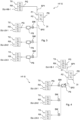
- Figure 1 shows a simple embodiment of an RF circuit HF-S with a first duplexer of a first frequency band DU-HB-1, a first duplexer of a second frequency band DU-LB-1 and a diplexer DI.
- the first duplexer of the second frequency band DU-LB-1 is connected to the second port P2 of the diplexer DI by a second signal path SP2.
- a phase shifter PS is connected in the second signal path SP2.
- the common port PG of the first duplexer of the first frequency band DU-HB-1 is connected to the first port P1 of the diplexer DI by a first signal path SP1.
- the common port PG of the diplexer DI can be connected to an antenna of a communications device.
- Each of the two duplexers has a transmit port TX and a receive port RX.
- the two duplexers can be connected to one or more transceiver circuits of a mobile radio device via the transmit and receive ports.
- a transmission signal is coupled in via both transmission ports TX of both duplexers, which reaches the diplexer DI via the signal paths SP1 and SP2. Due to the finite isolation of the diplexer DI, part of the transmission signal from the first frequency band is coupled into the second signal path SP2 in the direction of the duplexer of the second frequency band.
- the duplexers themselves are circuits with non-exclusively linear behavior, whereby in this case various TX signals meet at the TX filter of the duplexer of the second frequency band DU-LB-1.
- a signal leaking from the diplexer DI into the second signal path 2 is shifted in its phase position by the phase shifter in such a way that mixing with the transmission signal for the second signal path SP2 at the duplexer cannot take place.
- the formation of the intermodulation product at 886 MHz is prevented or its intensity is weakened so that reception is possible without any problems.
- FIG. 2 shows an embodiment in which three duplexers DU-HB-1, DU-HB-2, DU-HB-3 are provided for the first frequency band. Using an individual switch SW, each of the duplexers can be coupled to the first signal path SP1.
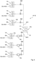
- Figure 3 an embodiment of an RF circuit HF-S, in which three duplexers DU-LB-1, DU-LB-2, DU-LB-3 of the second frequency band are provided.
- Each of the three duplexers can be individually coupled to the second signal path SP2 using switches.
- Each of the three duplexers can have a phase shifter PS specially assigned to it. The switches are preferably connected between the phase shifters and the diplexer.
- FIG 4 shows how a single phase shifter can be connected in the second signal path SP2 instead of the three different phase shifters.
- This phase shifter PS is intended and suitable for
- Figure 5 shows an embodiment in which three duplexers are provided in both the first frequency band and the second frequency band.
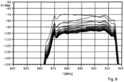
- Figure 6 shows characteristic curves of a typical diplexer with relatively low isolation.
- Figure 7 shows characteristic curves of a typical diplexer with higher isolation.
- Figure 8 shows the strength of the intermodulation interference in a carrier aggregation of the two Tx bands B5 and B7, when the diplexer of the Fig.6 is used.
- the different curves each represent a different phase shift caused by the phase shifter.
- the RF circuit includes a tunable phase shifter as a phase shifter, the phase shift of which is adjustable. Depending on the selected phase shift, an intermodulation interference reduction of up to about 30 dB can be achieved.
- Figure 9 different isolation values of an RF circuit, which determine the "better" diplexer of the Figure 7 with increased isolation - in addition to a tunable phase shifter as a phase shifter.
- the different in Figure 8 The curves shown represent the insulation values with varied phase offset by the phase shifter. Analogous to the Figure 7 The reduction of intermodulation interference can be improved by up to 30 dB by choosing an appropriate phase shift.
- Figure 10 shows the intensity of intermodulation products for RF circuits, each with one of the two Figure 6 shown diplexers and a phase shifter designed as a phase shifter. It turns out that the improved isolation actually leads to a reduction in the intermodulation products - but only if the phase shifter is optimally dimensioned or adjusted accordingly.
- the RF circuit is not limited to the embodiments described or shown.
- An RF circuit can in particular contain further circuit components, signal paths, filters, switches.
Landscapes
- Engineering & Computer Science (AREA)
- Computer Networks & Wireless Communication (AREA)
- Signal Processing (AREA)
- Transceivers (AREA)
Applications Claiming Priority (2)
| Application Number | Priority Date | Filing Date | Title |
|---|---|---|---|
| DE102015107305.6A DE102015107305B4 (de) | 2015-05-11 | 2015-05-11 | HF-Schaltung und Frontend-Schaltung mit HF-Schaltung |
| PCT/EP2016/058917 WO2016180613A1 (de) | 2015-05-11 | 2016-04-21 | Hf-schaltung und frontend-schaltung mit hf-schaltung |
Publications (2)
| Publication Number | Publication Date |
|---|---|
| EP3295570A1 EP3295570A1 (de) | 2018-03-21 |
| EP3295570B1 true EP3295570B1 (de) | 2024-07-24 |
Family
ID=55953113
Family Applications (1)
| Application Number | Title | Priority Date | Filing Date |
|---|---|---|---|
| EP16721374.3A Active EP3295570B1 (de) | 2015-05-11 | 2016-04-21 | Hf-schaltung und frontend-schaltung mit hf-schaltung |
Country Status (7)
| Country | Link |
|---|---|
| US (1) | US10530415B2 (enExample) |
| EP (1) | EP3295570B1 (enExample) |
| JP (1) | JP6833719B2 (enExample) |
| KR (2) | KR20240032160A (enExample) |
| CN (1) | CN107534451B (enExample) |
| DE (1) | DE102015107305B4 (enExample) |
| WO (1) | WO2016180613A1 (enExample) |
Families Citing this family (2)
| Publication number | Priority date | Publication date | Assignee | Title |
|---|---|---|---|---|
| CN107508606B (zh) * | 2017-07-25 | 2021-01-26 | Oppo广东移动通信有限公司 | 射频电路、天线装置及电子设备 |
| US11646782B2 (en) * | 2019-05-12 | 2023-05-09 | Skyworks Solutions, Inc. | Carrier aggregation circuit having multi-stage filter combination |
Citations (1)
| Publication number | Priority date | Publication date | Assignee | Title |
|---|---|---|---|---|
| KR20070068103A (ko) * | 2005-12-26 | 2007-06-29 | 엘지이노텍 주식회사 | 다중대역 스위치 모듈 |
Family Cites Families (12)
| Publication number | Priority date | Publication date | Assignee | Title |
|---|---|---|---|---|
| JP3891096B2 (ja) * | 2001-12-28 | 2007-03-07 | 株式会社村田製作所 | 信号受信回路およびそれを備えた通信機 |
| US7212789B2 (en) | 2002-12-30 | 2007-05-01 | Motorola, Inc. | Tunable duplexer |
| US7049906B2 (en) * | 2003-05-29 | 2006-05-23 | Sony Ericsson Mobile Communications Ab | Quad band antenna interface modules including matching network ports |
| JP4029779B2 (ja) | 2003-06-05 | 2008-01-09 | 株式会社村田製作所 | 高周波モジュールおよび通信装置 |
| TWI229974B (en) * | 2004-01-07 | 2005-03-21 | Darfon Electronics Corp | Diplexer and multi-layered diplexer |
| JP2005268878A (ja) * | 2004-03-16 | 2005-09-29 | Matsushita Electric Ind Co Ltd | アンテナ共用器 |
| US20070173210A1 (en) * | 2006-01-26 | 2007-07-26 | Lg Innotek Co., Ltd | Signal processing apparatus |
| CN101442838A (zh) | 2007-11-23 | 2009-05-27 | Nxp股份有限公司 | 使用双工器实现多模待机终端的系统 |
| JP5758754B2 (ja) * | 2011-09-09 | 2015-08-05 | 太陽誘電株式会社 | 電子部品 |
| US9722639B2 (en) * | 2013-05-01 | 2017-08-01 | Qorvo Us, Inc. | Carrier aggregation arrangements for mobile devices |
| US9438186B2 (en) * | 2014-04-30 | 2016-09-06 | Freescale Semiconductor, Inc. | Power amplifier with envelope injection |
| US9972893B2 (en) * | 2015-12-29 | 2018-05-15 | Commscope Technologies Llc | Duplexed phased array antennas |
-
2015
- 2015-05-11 DE DE102015107305.6A patent/DE102015107305B4/de active Active
-
2016
- 2016-04-21 US US15/564,675 patent/US10530415B2/en active Active
- 2016-04-21 WO PCT/EP2016/058917 patent/WO2016180613A1/de not_active Ceased
- 2016-04-21 KR KR1020247006334A patent/KR20240032160A/ko not_active Ceased
- 2016-04-21 EP EP16721374.3A patent/EP3295570B1/de active Active
- 2016-04-21 CN CN201680022029.7A patent/CN107534451B/zh active Active
- 2016-04-21 JP JP2017558734A patent/JP6833719B2/ja not_active Expired - Fee Related
- 2016-04-21 KR KR1020177030083A patent/KR20180004118A/ko not_active Ceased
Patent Citations (1)
| Publication number | Priority date | Publication date | Assignee | Title |
|---|---|---|---|---|
| KR20070068103A (ko) * | 2005-12-26 | 2007-06-29 | 엘지이노텍 주식회사 | 다중대역 스위치 모듈 |
Also Published As
| Publication number | Publication date |
|---|---|
| CN107534451B (zh) | 2020-12-11 |
| JP6833719B2 (ja) | 2021-02-24 |
| US20180076846A1 (en) | 2018-03-15 |
| DE102015107305A1 (de) | 2016-11-17 |
| CN107534451A (zh) | 2018-01-02 |
| JP2018518890A (ja) | 2018-07-12 |
| EP3295570A1 (de) | 2018-03-21 |
| KR20240032160A (ko) | 2024-03-08 |
| US10530415B2 (en) | 2020-01-07 |
| KR20180004118A (ko) | 2018-01-10 |
| WO2016180613A1 (de) | 2016-11-17 |
| DE102015107305B4 (de) | 2025-05-08 |
Similar Documents
| Publication | Publication Date | Title |
|---|---|---|
| DE102010046677B4 (de) | Schaltungsanordnung | |
| DE19823049C2 (de) | Leistungsverstärker-Ausgangsschaltung zur Unterdrückung von Oberschwingungen für eine Mobilfunkeinheit mit Doppelbandbetrieb und Verfahren zum Betreiben derselben | |
| DE102015122185B4 (de) | Multiplexervorrichtung mit einer ersten und einer zweiten Filtereinrichtung, die mit einem gemeinsamen Anschluss verbunden sind | |
| DE10053205B4 (de) | Kombinierte Frontendschaltung für drahtlose Übertragungssysteme | |
| DE102011012927B4 (de) | Verstärkermodul | |
| DE10316719A1 (de) | Frontendschaltung für drahtlose Übertragungssysteme | |
| DE10200048B4 (de) | Verbindung der Sende- und Empfangseinrichtungen von Multiband-/Multimode-Funkgeräten mit einer oder mehreren Antennen | |
| EP3292634B1 (de) | Hf-schaltung und hf-modul | |
| DE102014102699A1 (de) | Front-end Schaltung | |
| WO2009053288A1 (de) | Schaltungsanordnung für eine mobilfunkeinrichtung und verfahren zum betrieb | |
| DE112013006963T5 (de) | Schaltungsanorderung | |
| DE202020106896U1 (de) | Hochfrequenzmodul und Kommunikationsgerät | |
| DE102011018918B4 (de) | Schaltungsanordnung | |
| EP3295570B1 (de) | Hf-schaltung und frontend-schaltung mit hf-schaltung | |
| WO2005034376A1 (de) | Verfahren und vorrichtung zum verbinden der sende- und empfangseinrichtungen von multiband-/multimode-funkgeräten mit einer oder mehreren teilweise gemeinsam genutzten antennen | |
| DE102004040967A1 (de) | Schaltung mit hoher Isolation zwischen Sende- und Empfangspfad und Bauelement mit der Schaltung | |
| DE102016107628A1 (de) | Multiplexer-Schaltung für Tx-Carrier-Aggregation | |
| DE10315046B4 (de) | Schaltungsanordnung für ein Kommunikationsendgerät mit Multi-Mode-Betrieb | |
| DE102014113052B4 (de) | HF-Filtermodul mit verbesserter Erweiterbarkeit und Verwendung | |
| DE102013111798B4 (de) | Duplexer | |
| EP1505682A1 (de) | HF-Schaltungsanordnung für mobile Kommunikationsendgeräte | |
| DE102010055668B4 (de) | Schalteranordnung | |
| DE102004033835A1 (de) | Vorrichtung zur Verwendung externer Antennen mit einem mobilen Kommunikationsendgerät | |
| WO2007138073A2 (de) | Sende-/empfangsanordnung und verfahren zur signalverarbeitung in einer sende-/empfangsanordnung | |
| DE102005047135A1 (de) | Filteranordnung und Verfahren zum Filtern eines Signals |
Legal Events
| Date | Code | Title | Description |
|---|---|---|---|
| STAA | Information on the status of an ep patent application or granted ep patent |
Free format text: STATUS: THE INTERNATIONAL PUBLICATION HAS BEEN MADE |
|
| PUAI | Public reference made under article 153(3) epc to a published international application that has entered the european phase |
Free format text: ORIGINAL CODE: 0009012 |
|
| STAA | Information on the status of an ep patent application or granted ep patent |
Free format text: STATUS: REQUEST FOR EXAMINATION WAS MADE |
|
| 17P | Request for examination filed |
Effective date: 20171110 |
|
| AK | Designated contracting states |
Kind code of ref document: A1 Designated state(s): AL AT BE BG CH CY CZ DE DK EE ES FI FR GB GR HR HU IE IS IT LI LT LU LV MC MK MT NL NO PL PT RO RS SE SI SK SM TR |
|
| AX | Request for extension of the european patent |
Extension state: BA ME |
|
| DAV | Request for validation of the european patent (deleted) | ||
| DAX | Request for extension of the european patent (deleted) | ||
| STAA | Information on the status of an ep patent application or granted ep patent |
Free format text: STATUS: EXAMINATION IS IN PROGRESS |
|
| 17Q | First examination report despatched |
Effective date: 20210517 |
|
| GRAP | Despatch of communication of intention to grant a patent |
Free format text: ORIGINAL CODE: EPIDOSNIGR1 |
|
| STAA | Information on the status of an ep patent application or granted ep patent |
Free format text: STATUS: GRANT OF PATENT IS INTENDED |
|
| INTG | Intention to grant announced |
Effective date: 20240304 |
|
| GRAS | Grant fee paid |
Free format text: ORIGINAL CODE: EPIDOSNIGR3 |
|
| GRAA | (expected) grant |
Free format text: ORIGINAL CODE: 0009210 |
|
| STAA | Information on the status of an ep patent application or granted ep patent |
Free format text: STATUS: THE PATENT HAS BEEN GRANTED |
|
| AK | Designated contracting states |
Kind code of ref document: B1 Designated state(s): AL AT BE BG CH CY CZ DE DK EE ES FI FR GB GR HR HU IE IS IT LI LT LU LV MC MK MT NL NO PL PT RO RS SE SI SK SM TR |
|
| REG | Reference to a national code |
Ref country code: GB Ref legal event code: FG4D Free format text: NOT ENGLISH |
|
| REG | Reference to a national code |
Ref country code: CH Ref legal event code: EP |
|
| REG | Reference to a national code |
Ref country code: IE Ref legal event code: FG4D Free format text: LANGUAGE OF EP DOCUMENT: GERMAN Ref country code: DE Ref legal event code: R096 Ref document number: 502016016643 Country of ref document: DE |
|
| REG | Reference to a national code |
Ref country code: LT Ref legal event code: MG9D |
|
| REG | Reference to a national code |
Ref country code: NL Ref legal event code: MP Effective date: 20240724 |
|
| PG25 | Lapsed in a contracting state [announced via postgrant information from national office to epo] |
Ref country code: PT Free format text: LAPSE BECAUSE OF FAILURE TO SUBMIT A TRANSLATION OF THE DESCRIPTION OR TO PAY THE FEE WITHIN THE PRESCRIBED TIME-LIMIT Effective date: 20241125 |
|
| PG25 | Lapsed in a contracting state [announced via postgrant information from national office to epo] |
Ref country code: NL Free format text: LAPSE BECAUSE OF FAILURE TO SUBMIT A TRANSLATION OF THE DESCRIPTION OR TO PAY THE FEE WITHIN THE PRESCRIBED TIME-LIMIT Effective date: 20240724 |
|
| PG25 | Lapsed in a contracting state [announced via postgrant information from national office to epo] |
Ref country code: PT Free format text: LAPSE BECAUSE OF FAILURE TO SUBMIT A TRANSLATION OF THE DESCRIPTION OR TO PAY THE FEE WITHIN THE PRESCRIBED TIME-LIMIT Effective date: 20241125 Ref country code: NL Free format text: LAPSE BECAUSE OF FAILURE TO SUBMIT A TRANSLATION OF THE DESCRIPTION OR TO PAY THE FEE WITHIN THE PRESCRIBED TIME-LIMIT Effective date: 20240724 |
|
| PG25 | Lapsed in a contracting state [announced via postgrant information from national office to epo] |
Ref country code: NO Free format text: LAPSE BECAUSE OF FAILURE TO SUBMIT A TRANSLATION OF THE DESCRIPTION OR TO PAY THE FEE WITHIN THE PRESCRIBED TIME-LIMIT Effective date: 20241024 |
|
| PG25 | Lapsed in a contracting state [announced via postgrant information from national office to epo] |
Ref country code: GR Free format text: LAPSE BECAUSE OF FAILURE TO SUBMIT A TRANSLATION OF THE DESCRIPTION OR TO PAY THE FEE WITHIN THE PRESCRIBED TIME-LIMIT Effective date: 20241025 Ref country code: FI Free format text: LAPSE BECAUSE OF FAILURE TO SUBMIT A TRANSLATION OF THE DESCRIPTION OR TO PAY THE FEE WITHIN THE PRESCRIBED TIME-LIMIT Effective date: 20240724 Ref country code: PL Free format text: LAPSE BECAUSE OF FAILURE TO SUBMIT A TRANSLATION OF THE DESCRIPTION OR TO PAY THE FEE WITHIN THE PRESCRIBED TIME-LIMIT Effective date: 20240724 |
|
| PG25 | Lapsed in a contracting state [announced via postgrant information from national office to epo] |
Ref country code: BG Free format text: LAPSE BECAUSE OF FAILURE TO SUBMIT A TRANSLATION OF THE DESCRIPTION OR TO PAY THE FEE WITHIN THE PRESCRIBED TIME-LIMIT Effective date: 20240724 |
|
| PG25 | Lapsed in a contracting state [announced via postgrant information from national office to epo] |
Ref country code: LV Free format text: LAPSE BECAUSE OF FAILURE TO SUBMIT A TRANSLATION OF THE DESCRIPTION OR TO PAY THE FEE WITHIN THE PRESCRIBED TIME-LIMIT Effective date: 20240724 |
|
| PG25 | Lapsed in a contracting state [announced via postgrant information from national office to epo] |
Ref country code: IS Free format text: LAPSE BECAUSE OF FAILURE TO SUBMIT A TRANSLATION OF THE DESCRIPTION OR TO PAY THE FEE WITHIN THE PRESCRIBED TIME-LIMIT Effective date: 20241124 |
|
| PG25 | Lapsed in a contracting state [announced via postgrant information from national office to epo] |
Ref country code: HR Free format text: LAPSE BECAUSE OF FAILURE TO SUBMIT A TRANSLATION OF THE DESCRIPTION OR TO PAY THE FEE WITHIN THE PRESCRIBED TIME-LIMIT Effective date: 20240724 |
|
| PG25 | Lapsed in a contracting state [announced via postgrant information from national office to epo] |
Ref country code: ES Free format text: LAPSE BECAUSE OF FAILURE TO SUBMIT A TRANSLATION OF THE DESCRIPTION OR TO PAY THE FEE WITHIN THE PRESCRIBED TIME-LIMIT Effective date: 20240724 Ref country code: RS Free format text: LAPSE BECAUSE OF FAILURE TO SUBMIT A TRANSLATION OF THE DESCRIPTION OR TO PAY THE FEE WITHIN THE PRESCRIBED TIME-LIMIT Effective date: 20241024 |
|
| PG25 | Lapsed in a contracting state [announced via postgrant information from national office to epo] |
Ref country code: RS Free format text: LAPSE BECAUSE OF FAILURE TO SUBMIT A TRANSLATION OF THE DESCRIPTION OR TO PAY THE FEE WITHIN THE PRESCRIBED TIME-LIMIT Effective date: 20241024 Ref country code: PL Free format text: LAPSE BECAUSE OF FAILURE TO SUBMIT A TRANSLATION OF THE DESCRIPTION OR TO PAY THE FEE WITHIN THE PRESCRIBED TIME-LIMIT Effective date: 20240724 Ref country code: NO Free format text: LAPSE BECAUSE OF FAILURE TO SUBMIT A TRANSLATION OF THE DESCRIPTION OR TO PAY THE FEE WITHIN THE PRESCRIBED TIME-LIMIT Effective date: 20241024 Ref country code: LV Free format text: LAPSE BECAUSE OF FAILURE TO SUBMIT A TRANSLATION OF THE DESCRIPTION OR TO PAY THE FEE WITHIN THE PRESCRIBED TIME-LIMIT Effective date: 20240724 Ref country code: IS Free format text: LAPSE BECAUSE OF FAILURE TO SUBMIT A TRANSLATION OF THE DESCRIPTION OR TO PAY THE FEE WITHIN THE PRESCRIBED TIME-LIMIT Effective date: 20241124 Ref country code: HR Free format text: LAPSE BECAUSE OF FAILURE TO SUBMIT A TRANSLATION OF THE DESCRIPTION OR TO PAY THE FEE WITHIN THE PRESCRIBED TIME-LIMIT Effective date: 20240724 Ref country code: GR Free format text: LAPSE BECAUSE OF FAILURE TO SUBMIT A TRANSLATION OF THE DESCRIPTION OR TO PAY THE FEE WITHIN THE PRESCRIBED TIME-LIMIT Effective date: 20241025 Ref country code: FI Free format text: LAPSE BECAUSE OF FAILURE TO SUBMIT A TRANSLATION OF THE DESCRIPTION OR TO PAY THE FEE WITHIN THE PRESCRIBED TIME-LIMIT Effective date: 20240724 Ref country code: ES Free format text: LAPSE BECAUSE OF FAILURE TO SUBMIT A TRANSLATION OF THE DESCRIPTION OR TO PAY THE FEE WITHIN THE PRESCRIBED TIME-LIMIT Effective date: 20240724 Ref country code: BG Free format text: LAPSE BECAUSE OF FAILURE TO SUBMIT A TRANSLATION OF THE DESCRIPTION OR TO PAY THE FEE WITHIN THE PRESCRIBED TIME-LIMIT Effective date: 20240724 |
|
| PG25 | Lapsed in a contracting state [announced via postgrant information from national office to epo] |
Ref country code: RO Free format text: LAPSE BECAUSE OF FAILURE TO SUBMIT A TRANSLATION OF THE DESCRIPTION OR TO PAY THE FEE WITHIN THE PRESCRIBED TIME-LIMIT Effective date: 20240724 Ref country code: DK Free format text: LAPSE BECAUSE OF FAILURE TO SUBMIT A TRANSLATION OF THE DESCRIPTION OR TO PAY THE FEE WITHIN THE PRESCRIBED TIME-LIMIT Effective date: 20240724 Ref country code: SM Free format text: LAPSE BECAUSE OF FAILURE TO SUBMIT A TRANSLATION OF THE DESCRIPTION OR TO PAY THE FEE WITHIN THE PRESCRIBED TIME-LIMIT Effective date: 20240724 |
|
| PG25 | Lapsed in a contracting state [announced via postgrant information from national office to epo] |
Ref country code: EE Free format text: LAPSE BECAUSE OF FAILURE TO SUBMIT A TRANSLATION OF THE DESCRIPTION OR TO PAY THE FEE WITHIN THE PRESCRIBED TIME-LIMIT Effective date: 20240724 |
|
| PG25 | Lapsed in a contracting state [announced via postgrant information from national office to epo] |
Ref country code: CZ Free format text: LAPSE BECAUSE OF FAILURE TO SUBMIT A TRANSLATION OF THE DESCRIPTION OR TO PAY THE FEE WITHIN THE PRESCRIBED TIME-LIMIT Effective date: 20240724 |
|
| PGFP | Annual fee paid to national office [announced via postgrant information from national office to epo] |
Ref country code: FR Payment date: 20250319 Year of fee payment: 10 |
|
| REG | Reference to a national code |
Ref country code: DE Ref legal event code: R097 Ref document number: 502016016643 Country of ref document: DE |
|
| PG25 | Lapsed in a contracting state [announced via postgrant information from national office to epo] |
Ref country code: SK Free format text: LAPSE BECAUSE OF FAILURE TO SUBMIT A TRANSLATION OF THE DESCRIPTION OR TO PAY THE FEE WITHIN THE PRESCRIBED TIME-LIMIT Effective date: 20240724 Ref country code: IT Free format text: LAPSE BECAUSE OF FAILURE TO SUBMIT A TRANSLATION OF THE DESCRIPTION OR TO PAY THE FEE WITHIN THE PRESCRIBED TIME-LIMIT Effective date: 20240724 |
|
| PGFP | Annual fee paid to national office [announced via postgrant information from national office to epo] |
Ref country code: GB Payment date: 20250313 Year of fee payment: 10 |
|
| PLBE | No opposition filed within time limit |
Free format text: ORIGINAL CODE: 0009261 |
|
| STAA | Information on the status of an ep patent application or granted ep patent |
Free format text: STATUS: NO OPPOSITION FILED WITHIN TIME LIMIT |
|
| 26N | No opposition filed |
Effective date: 20250425 |
|
| PGFP | Annual fee paid to national office [announced via postgrant information from national office to epo] |
Ref country code: DE Payment date: 20250317 Year of fee payment: 10 |
|
| PG25 | Lapsed in a contracting state [announced via postgrant information from national office to epo] |
Ref country code: SE Free format text: LAPSE BECAUSE OF FAILURE TO SUBMIT A TRANSLATION OF THE DESCRIPTION OR TO PAY THE FEE WITHIN THE PRESCRIBED TIME-LIMIT Effective date: 20240724 |
|
| REG | Reference to a national code |
Ref country code: CH Ref legal event code: H13 Free format text: ST27 STATUS EVENT CODE: U-0-0-H10-H13 (AS PROVIDED BY THE NATIONAL OFFICE) Effective date: 20251125 |