EP3293879A2 - Rauschunterdrückungstechnik in einem vorwärtsgekoppelten betriebsverstärker und dazugehöriger filter und delta-sigma modulator - Google Patents
Rauschunterdrückungstechnik in einem vorwärtsgekoppelten betriebsverstärker und dazugehöriger filter und delta-sigma modulator Download PDFInfo
- Publication number
- EP3293879A2 EP3293879A2 EP17184344.4A EP17184344A EP3293879A2 EP 3293879 A2 EP3293879 A2 EP 3293879A2 EP 17184344 A EP17184344 A EP 17184344A EP 3293879 A2 EP3293879 A2 EP 3293879A2
- Authority
- EP
- European Patent Office
- Prior art keywords
- circuit
- noise
- signal
- input signal
- amplified
- Prior art date
- Legal status (The legal status is an assumption and is not a legal conclusion. Google has not performed a legal analysis and makes no representation as to the accuracy of the status listed.)
- Withdrawn
Links
- 238000000034 method Methods 0.000 title description 5
- 238000000605 extraction Methods 0.000 claims abstract description 74
- 239000003990 capacitor Substances 0.000 description 6
- 238000013461 design Methods 0.000 description 4
- 238000010586 diagram Methods 0.000 description 4
- 238000004519 manufacturing process Methods 0.000 description 3
- 230000002238 attenuated effect Effects 0.000 description 2
- 238000012546 transfer Methods 0.000 description 2
- 238000012935 Averaging Methods 0.000 description 1
- 230000004075 alteration Effects 0.000 description 1
- 230000001010 compromised effect Effects 0.000 description 1
- 230000008878 coupling Effects 0.000 description 1
- 238000010168 coupling process Methods 0.000 description 1
- 238000005859 coupling reaction Methods 0.000 description 1
- 238000012986 modification Methods 0.000 description 1
- 230000004048 modification Effects 0.000 description 1
- 238000013139 quantization Methods 0.000 description 1
- 230000035945 sensitivity Effects 0.000 description 1
- 238000012360 testing method Methods 0.000 description 1
Images



Classifications
-
- H—ELECTRICITY
- H03—ELECTRONIC CIRCUITRY
- H03M—CODING; DECODING; CODE CONVERSION IN GENERAL
- H03M3/00—Conversion of analogue values to or from differential modulation
- H03M3/30—Delta-sigma modulation
- H03M3/322—Continuously compensating for, or preventing, undesired influence of physical parameters
- H03M3/368—Continuously compensating for, or preventing, undesired influence of physical parameters of noise other than the quantisation noise already being shaped inherently by delta-sigma modulators
-
- H—ELECTRICITY
- H03—ELECTRONIC CIRCUITRY
- H03F—AMPLIFIERS
- H03F1/00—Details of amplifiers with only discharge tubes, only semiconductor devices or only unspecified devices as amplifying elements
- H03F1/32—Modifications of amplifiers to reduce non-linear distortion
- H03F1/3223—Modifications of amplifiers to reduce non-linear distortion using feed-forward
-
- H—ELECTRICITY
- H03—ELECTRONIC CIRCUITRY
- H03F—AMPLIFIERS
- H03F1/00—Details of amplifiers with only discharge tubes, only semiconductor devices or only unspecified devices as amplifying elements
- H03F1/26—Modifications of amplifiers to reduce influence of noise generated by amplifying elements
-
- H—ELECTRICITY
- H03—ELECTRONIC CIRCUITRY
- H03F—AMPLIFIERS
- H03F1/00—Details of amplifiers with only discharge tubes, only semiconductor devices or only unspecified devices as amplifying elements
- H03F1/32—Modifications of amplifiers to reduce non-linear distortion
- H03F1/3223—Modifications of amplifiers to reduce non-linear distortion using feed-forward
- H03F1/3229—Modifications of amplifiers to reduce non-linear distortion using feed-forward using a loop for error extraction and another loop for error subtraction
-
- H—ELECTRICITY
- H03—ELECTRONIC CIRCUITRY
- H03F—AMPLIFIERS
- H03F1/00—Details of amplifiers with only discharge tubes, only semiconductor devices or only unspecified devices as amplifying elements
- H03F1/32—Modifications of amplifiers to reduce non-linear distortion
- H03F1/3241—Modifications of amplifiers to reduce non-linear distortion using predistortion circuits
- H03F1/3247—Modifications of amplifiers to reduce non-linear distortion using predistortion circuits using feedback acting on predistortion circuits
-
- H—ELECTRICITY
- H03—ELECTRONIC CIRCUITRY
- H03F—AMPLIFIERS
- H03F1/00—Details of amplifiers with only discharge tubes, only semiconductor devices or only unspecified devices as amplifying elements
- H03F1/38—Positive-feedback circuit arrangements without negative feedback
-
- H—ELECTRICITY
- H03—ELECTRONIC CIRCUITRY
- H03F—AMPLIFIERS
- H03F3/00—Amplifiers with only discharge tubes or only semiconductor devices as amplifying elements
- H03F3/45—Differential amplifiers
-
- H—ELECTRICITY
- H03—ELECTRONIC CIRCUITRY
- H03F—AMPLIFIERS
- H03F3/00—Amplifiers with only discharge tubes or only semiconductor devices as amplifying elements
- H03F3/45—Differential amplifiers
- H03F3/45071—Differential amplifiers with semiconductor devices only
- H03F3/45076—Differential amplifiers with semiconductor devices only characterised by the way of implementation of the active amplifying circuit in the differential amplifier
- H03F3/45475—Differential amplifiers with semiconductor devices only characterised by the way of implementation of the active amplifying circuit in the differential amplifier using IC blocks as the active amplifying circuit
-
- H—ELECTRICITY
- H03—ELECTRONIC CIRCUITRY
- H03G—CONTROL OF AMPLIFICATION
- H03G3/00—Gain control in amplifiers or frequency changers
- H03G3/20—Automatic control
- H03G3/30—Automatic control in amplifiers having semiconductor devices
- H03G3/3036—Automatic control in amplifiers having semiconductor devices in high-frequency amplifiers or in frequency-changers
-
- H—ELECTRICITY
- H03—ELECTRONIC CIRCUITRY
- H03M—CODING; DECODING; CODE CONVERSION IN GENERAL
- H03M3/00—Conversion of analogue values to or from differential modulation
- H03M3/30—Delta-sigma modulation
- H03M3/322—Continuously compensating for, or preventing, undesired influence of physical parameters
- H03M3/324—Continuously compensating for, or preventing, undesired influence of physical parameters characterised by means or methods for compensating or preventing more than one type of error at a time, e.g. by synchronisation or using a ratiometric arrangement
- H03M3/344—Continuously compensating for, or preventing, undesired influence of physical parameters characterised by means or methods for compensating or preventing more than one type of error at a time, e.g. by synchronisation or using a ratiometric arrangement by filtering other than the noise-shaping inherent to delta-sigma modulators, e.g. anti-aliasing
-
- H—ELECTRICITY
- H03—ELECTRONIC CIRCUITRY
- H03M—CODING; DECODING; CODE CONVERSION IN GENERAL
- H03M3/00—Conversion of analogue values to or from differential modulation
- H03M3/30—Delta-sigma modulation
- H03M3/39—Structural details of delta-sigma modulators, e.g. incremental delta-sigma modulators
- H03M3/412—Structural details of delta-sigma modulators, e.g. incremental delta-sigma modulators characterised by the number of quantisers and their type and resolution
- H03M3/422—Structural details of delta-sigma modulators, e.g. incremental delta-sigma modulators characterised by the number of quantisers and their type and resolution having one quantiser only
-
- H—ELECTRICITY
- H03—ELECTRONIC CIRCUITRY
- H03M—CODING; DECODING; CODE CONVERSION IN GENERAL
- H03M3/00—Conversion of analogue values to or from differential modulation
- H03M3/30—Delta-sigma modulation
- H03M3/39—Structural details of delta-sigma modulators, e.g. incremental delta-sigma modulators
- H03M3/436—Structural details of delta-sigma modulators, e.g. incremental delta-sigma modulators characterised by the order of the loop filter, e.g. error feedback type
-
- H—ELECTRICITY
- H03—ELECTRONIC CIRCUITRY
- H03M—CODING; DECODING; CODE CONVERSION IN GENERAL
- H03M3/00—Conversion of analogue values to or from differential modulation
- H03M3/30—Delta-sigma modulation
- H03M3/458—Analogue/digital converters using delta-sigma modulation as an intermediate step
-
- H—ELECTRICITY
- H03—ELECTRONIC CIRCUITRY
- H03F—AMPLIFIERS
- H03F2200/00—Indexing scheme relating to amplifiers
- H03F2200/411—Indexing scheme relating to amplifiers the output amplifying stage of an amplifier comprising two power stages
-
- H—ELECTRICITY
- H03—ELECTRONIC CIRCUITRY
- H03F—AMPLIFIERS
- H03F2203/00—Indexing scheme relating to amplifiers with only discharge tubes or only semiconductor devices as amplifying elements covered by H03F3/00
- H03F2203/45—Indexing scheme relating to differential amplifiers
- H03F2203/45116—Feedback coupled to the input of the differential amplifier
-
- H—ELECTRICITY
- H03—ELECTRONIC CIRCUITRY
- H03G—CONTROL OF AMPLIFICATION
- H03G3/00—Gain control in amplifiers or frequency changers
- H03G3/20—Automatic control
Definitions
- Base-band receiver noise is always dominated by a channel selecting filter with embedded programmable gain amplifier (PGA) function.
- PGA programmable gain amplifier
- ADC analog-to-digital converter
- blocker rejection is conventionally designed to be second or third order.
- the noise reduction is always compromised with the operational amplifier stability in a power inefficient manner, especially in the receiver sensitivity test.
- a filter comprises a first amplifying stage, a noise extraction circuit and a noise cancellation circuit.
- the first amplifying stage is arranged for receiving an input signal to generate an amplified input signal.
- the noise extraction circuit is coupled to the first amplifying stage, and is arranged for receiving at least the amplified input signal to generate a noise signal associated with noise components of the amplified input signal.
- the input signal is also coupled to the noise extraction circuit to remove the amplified input signal.
- the noise cancellation circuit is coupled to the first amplifying stage and the noise extraction circuit, and is arranged for cancelling noise components of the amplified input signal by using the noise signal generated by the noise extraction circuit, to generate a noise-cancelled amplified input signal.
- a delta-sigma modulator comprises a receiving circuit, a loop filter, a quantizer and a feedback circuit.
- the receiving circuit is arranged for receiving an input signal and a feedback signal to generate a subtraction signal.
- the loop filter is coupled to the receiving circuit, and is arranged for receiving the subtraction signal to generate a filtered subtraction signal.
- the quantizer is coupled to the loop filter, and is arranged for generating a digital output signal according to the filtered subtraction signal.
- the feedback circuit is arranged for receiving the digital output signal to generate the feedback signal.
- the loop filter comprises a first amplifying stage, a noise extraction circuit and a noise cancellation circuit.
- the first amplifying stage is arranged for receiving the subtraction signal to generate an amplified subtraction signal.
- the noise extraction circuit is coupled to the first amplifying stage, and is arranged for receiving at least the amplified subtraction signal to generate a noise signal associated with noise components of the amplified subtraction signal.
- the subtraction signal from the difference between input signal and feedback one is extracted inside the first amplifying stage and also coupled to the noise extraction circuit to remove the amplified subtraction signal.
- the noise cancellation circuit is coupled to the first amplifying stage and the noise extraction circuit, and is arranged for cancelling noise components of the amplified subtraction signal by using the noise signal generated by the noise extraction circuit, to generate a noise-cancelled amplified subtraction signal.
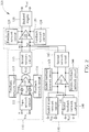
- FIG. 1 is a diagram illustrating a filter 100 with programmable gain amplifier function according to one embodiment of the present invention.
- the filter 100 comprises a first amplifying stage 110, a second amplifying stage 120, one or more backend stages 130 and a noise extraction circuit 140.
- the first amplifying stage 110 comprises an input network circuit 111, an operational amplifier 112, two feedback network circuits 113 and 114, and a second network circuit 115, where the operational amplifier 112 receives an input signal Vin via the input network circuit 110 to generate an amplified input signal Vo1, the feedback network circuit 113 is coupled between a positive input terminal and a negative output terminal of the operational amplifier 112, the feedback network circuit 114 is coupled between a negative input terminal and a positive output terminal of the operational amplifier 112, and the amplified input signal Vo1 is transmitted to the second amplifying stage 120 via the second network circuit 115.
- the second amplifying stage 120 comprises an operational amplifier 122 and two feedback network circuits 123 and 124, where the feedback network circuit 123 is coupled between a positive input terminal and a negative output terminal of the operational amplifier 122, the feedback network circuit 124 is coupled between a negative input terminal and a positive output terminal of the operational amplifier 122.
- the amplified input signal Vo1 may have obvious noise components.
- the input signal Vin is coupled to the noise extraction circuit 140 to remove the amplified input signal Vo1 at the output of the noise extraction circuit 140.
- the noise extraction circuit 140 provides a noise signal that is equivalent to the noise components of the amplified input signal Vo1, and a noise cancellation circuit (which is implemented by nodes N1 and N2 shown in FIG. 1 ) cancels or alleviates the noise components of the amplified input signal Vo1 by using the noise signal generated by the noise extraction circuit 140, to generate a noise-cancelled amplified input signal.
- the noise-cancelled amplified input signal is processed by the second amplifying stage 120 and the backend stages 130 to generate an output signal Vout.
- the noise signal generated by the noise extraction circuit 140 is a current signal
- the amplified input signal Vo1 is transformed to be current signals by using the second network circuit 115. Therefore, the noise-cancelled amplified input signal can be simply obtained by using the nodes N1 and N2 to combine the amplified input signal Vo1 and the noise signal.
- FIG. 2 shows an example of the noise extraction circuit 140.
- the noise extraction circuit 140 comprises a scaled input network circuit 141, an auxiliary operational amplifier 142, three scaled feedback network circuits 143, 144 and 146, and a second network circuit 145.
- the scaled input network circuit 141 and the scaled feedback network circuit 146 are coupled between the input signal Vin and the auxiliary operational amplifier 142.
- the scalded feedback network circuit 143 is coupled between a positive input terminal and a negative output terminal of the auxiliary operational amplifier 142.
- the scalded feedback network circuit 144 is coupled between a negative input terminal and a positive output terminal of the auxiliary operational amplifier 142.
- the second network circuit 145 is coupled between the auxiliary operational amplifier 142 and the nodes N1 and N2.
- the circuit blocks of the noise extraction circuit 140 and the corresponding circuit blocks of the first amplifying stage 110 have the same structure with difference sizes, and their scaling factors are the same.
- a size of the scaled input network circuit 141 may be one-tenth of a size of the input network circuit 111
- a size of the scaled feedback network circuit 143, 144 or 146 may be one-tenth of a size of the feedback network circuit 113 or 114
- a size of the second scaled network circuit 145 is the same as second network circuit 115. Because a gain of the operational amplifier is determined based on a ratio between the feedback network circuit and the input network circuit, by using the aforementioned design, the operational amplifier 112 and the auxiliary operational amplifier 142 have the same transfer function.
- the scaled input network circuit 141 within the noise extraction circuit 140 receives the input signal in an inverse manner.
- the output of the auxiliary operational amplifier 142 can be exactly the noise components of the amplified input signal Vo1, without containing any signal component of the input signal Vin.
- the noise contributed by the second amplifying stage 120 or other circuits will not go back to the input nodes of the filter 100 via the noise extraction circuit 140, that is a noise level of the input signal Vin will not be influenced by arranging the noise extraction circuit 140 within the filter 100.
- FIG. 3 is a detailed circuit structure of the filter 100 according to one embodiment of the present invention.
- the input network circuit 111 is implemented by two resistors R0
- the feedback network circuit 113/114 is implemented by a resistor R1 and a capacitor C1
- the second network circuit 115 is implemented by two resistors R2.
- the feedback network circuit 123/124 is implemented by a resistor R3 and a capacitor C3.
- the scaled input network circuit 141 is implemented by two resistors R0'
- the scaled feedback network circuit 143/144/146 is implemented by a resistor R1' and a capacitor C1'
- the second network circuit 145 is implemented by two resistors R2.
- the scaling factors for each circuit within the noise extraction circuit 140 and the corresponding circuit within the first amplifying stage 110 are the same.
- a resistance of the resistor R1 is designed to be greater than a resistance of the resistor R0 to make the gain of the operational amplifier 112 greater than one
- a resistance of the resistor R1' is designed to be greater than a resistance of the resistor R0' to make the gain of the auxiliary operational amplifier 142 greater than one.
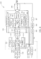
- FIG. 4 is a diagram illustrating a delta-sigma modulator 400 according to one embodiment of the present invention, where the delta-sigma modulator 400 is a continuous-time delta-sigma modulator type analog to digital converter (ADC).
- the delta-sigma modulator 400 comprises an input network circuit 402, a receiving circuit implemented by nodes Nin1 and Nin2, a loop filter 404, a quantizer 406, a phase delay/adjusting circuit 407, a data weighted averaging (DWA) circuit 408, and a digital-to-analog converters (DAC) 409.
- ADC analog to digital converter
- the receiving circuit Nin1 and Nin2 receive an input signal Vin and a feedback signal V FB , and calculates a difference by subtracting the feedback signal V FB by the input signal Vin to generate a subtraction signal. Then, the loop filter 404 filters the subtraction signal to generate a filtered subtraction signal. The quantizer 406 generates a digital output signal Dout according to the filtered subtraction signal. Then, the digital output signal Dout is processed by the phase delay/adjusting circuit 160, the DWA circuit 408, and the DAC 409 to generate the feedback signal V FB to the receiving circuit Nin1 and Nin2.
- the loop filter 404 comprises a first amplifying stage 410, a second amplifying stage 420, one or more backend stage(s) 430 and two feed-forward network circuit 432 and 434.
- the first amplifying stage 410 comprises an operational amplifier 412, two feedback network circuits 413 and 414 and a second network circuit 415, where the operational amplifier 412 receives the subtraction signal (i.e.
- the feedback network circuit 143 is coupled between a positive input terminal and a negative output terminal of the operational amplifier 412
- the feedback network circuit 414 is coupled between a negative input terminal and a positive output terminal of the operational amplifier 412
- the amplified subtraction signal Vo1 is transmitted to the second amplifying stage 420 via the second network circuit 415.
- the amplified subtraction signal Vo1 may have obvious noise components.
- the subtraction signal from the difference between input signal Vin and feedback one V FB is extracted inside the operational amplifier 412 and also coupled to the noise extraction circuit 440 to remove the amplified subtraction signal.
- the noise extraction circuit 440 provides a noise signal that is equivalent to the noise components of the amplified subtraction signal Vo1, and a noise cancellation circuit (which is implemented by nodes N1 and N2 shown in FIG.
- the noise-cancelled amplified input signal is processed by the second amplifying stage 440, the backend stages 430 and the quantizer 406 to generate the digital output signal Dout.
- the noise signal generated by the noise extraction circuit 440 is a current signal
- the amplified subtraction signal Vo1 is transformed to be current signals by using the second network circuit 415. Therefore, the noise-cancelled amplified subtraction signal can be simply obtained by using the nodes N1 and N2 to combine the amplified subtraction signal Vo1 and the noise signal.
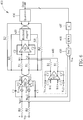
- FIG. 5 shows an example of the noise extraction circuit 440.
- the noise extraction circuit 440 comprises an auxiliary operational amplifier 442, three scaled feedback network circuits 441, 443, and 444, and a second network circuit 445.
- the scaled feedback network circuit 441 are coupled between the amplified subtraction signal Vo1 and the auxiliary operational amplifier 442.
- the scalded feedback network circuit 443 is coupled between a positive input terminal and a negative output terminal of the auxiliary operational amplifier 442.
- the scalded feedback network circuit 444 is coupled between a negative input terminal and a positive output terminal of the auxiliary operational amplifier 442.
- the second network circuit 445 is coupled between the auxiliary operational amplifier 442 and the nodes N1 and N2.
- the circuit blocks of the noise extraction circuit 440 and the corresponding circuit blocks of the first amplifying stage 410 have the same structure with difference sizes, and their scaling factors are the same.
- a size of the scaled feedback network circuit 441, 443 or 444 may be one-tenth of a size of the feedback network circuit 413 or 414
- a size of the second scaled network circuit 445 may also be one-tenth of a size of the second network circuit 415. Because a gain of the operational amplifier is determined based on a ratio between the feedback network circuit and the input network circuit, by using the aforementioned design, the operational amplifier 412 and the auxiliary operational amplifier 442 have the same transfer function.
- the subtraction signal generated by the receiving circuit Nin1 and Nin2 is a differential pair
- the amplified subtraction signal Vo1 generated by the operational amplifier 412 is also a differential pair comprising Vo1+ and Vo1-.
- the operational amplifier 412 also generates two current signals Io1+ and Io1-, where the current signal Io1+ is extracted from one of the subtraction signal pair, or the current signal Io1+ may be obtained from the subtraction signal pair (this current obtained from a current flowing through the feedback network circuit 414 with the scaling factor equal to that of the scaled feedback network circuit 444); and the current signal Io1- is extracted from the other one of the subtraction signal pair, or the current signal Io1- may be obtained from the other one of the subtraction signal pair (this current obtained from a current flowing through the feedback network circuit 413 with the scaling factor equal to that of the scaled feedback network circuit 443).
- the positive input terminal of the auxiliary operational amplifier 442 is coupled to the current signal Io1- and the subtraction signal Vo1+, and the negative input terminal of the auxiliary operational amplifier 442 is coupled to the current signal Io1+ and the subtraction signal Vo1-, and the scaled feedback network circuit 441, 443 or 444 are the same.
- the output of the auxiliary operational amplifier 442 can be exactly the same as noise components of the amplified subtraction signal Vo1, without containing any signal component of the input signal Vin or the subtraction signal.
- the noise contributed by the second amplifying stage 420 or other circuits will not go back to the input nodes of the delta-sigma modulator 400 via the noise extraction circuit 440, that is a noise level of the input signal Vin will not be influenced by arranging the noise extraction circuit 440 delta-sigma modulator 400.
- the noise contributed by the second amplifying stage 420 or other circuits may go back to the input nodes of the delta-sigma modulator 400 via the first amplifying stage 410.
- the gain of operational amplifier 412 is greater than one, and the noise contributed by the second amplifying stage 420 will be attenuated when passing through the first amplifying stage 410.
- FIG. 6 is a detailed circuit structure of the delta-sigma modulator 400 according to one embodiment of the present invention.
- the input network circuit 402 is implemented by two resistors R0.
- the feedback network circuit 413/414 is implemented by a capacitor C1
- a second network circuit 415 is implemented by two resistors R1.
- the feedback network circuit 423/424 is implemented by a capacitor C2.
- the scaled feedback network circuit 441/443/444 is implemented by a capacitor C1'
- a second network circuit 445 is implemented by two resistors R1.
- the feed-forward network circuit 432/434 is implemented by resistors R2 and R3.
- the scaling factors for each circuit within the noise extraction circuit 440 and the corresponding circuit within the first amplifying stage 410 are the same.
- a ratio between C1 and C1' in scaled feedback network 441/443/444 is the same.
- both the first amplifying stage 410 and the noise extraction circuit are an integrator, their gain are much greater than one.
- a noise extraction circuit is used to obtain the noise components of the output of the first amplifying stage, and the noise signal generated by the noise extraction circuit is forwarded to the input of the second amplifying stage to cancel or alleviate the noise components of the output of the first amplifying stage (or alleviate the noise components of the second amplifying stage).
- the noise extraction circuit has a smaller chip area to save the manufacturing cost, and the noise extraction circuit is designed to not generate any signal component to prevent the noise contributed by the second amplifying stage from going back to the input node. Therefore, the circuit of the present invention can effectively lower the noise without increasing too much chip area.
Landscapes
- Engineering & Computer Science (AREA)
- Power Engineering (AREA)
- Physics & Mathematics (AREA)
- Nonlinear Science (AREA)
- Theoretical Computer Science (AREA)
- Amplifiers (AREA)
- Compression, Expansion, Code Conversion, And Decoders (AREA)
Applications Claiming Priority (2)
| Application Number | Priority Date | Filing Date | Title |
|---|---|---|---|
| US201662375921P | 2016-08-17 | 2016-08-17 | |
| US15/652,207 US9929742B2 (en) | 2016-08-17 | 2017-07-17 | Feed-forward operational amplifier noise cancellation technique and associated filter and delta-sigma modulator |
Publications (2)
| Publication Number | Publication Date |
|---|---|
| EP3293879A2 true EP3293879A2 (de) | 2018-03-14 |
| EP3293879A3 EP3293879A3 (de) | 2018-04-11 |
Family
ID=59506198
Family Applications (1)
| Application Number | Title | Priority Date | Filing Date |
|---|---|---|---|
| EP17184344.4A Withdrawn EP3293879A3 (de) | 2016-08-17 | 2017-08-01 | Rauschunterdrückungstechnik in einem vorwärtsgekoppelten betriebsverstärker und dazugehöriger filter und delta-sigma modulator |
Country Status (4)
| Country | Link |
|---|---|
| US (1) | US9929742B2 (de) |
| EP (1) | EP3293879A3 (de) |
| CN (1) | CN107769735B (de) |
| TW (1) | TWI631816B (de) |
Family Cites Families (19)
| Publication number | Priority date | Publication date | Assignee | Title |
|---|---|---|---|---|
| US3980967A (en) | 1975-03-14 | 1976-09-14 | Bell Telephone Laboratories, Incorporated | Differential feedback amplifier with frequency-shaped reference signal |
| US4276514A (en) | 1979-07-09 | 1981-06-30 | Trw Inc. | Wideband, phase compensated amplifier with negative feedback of distortion components in the output signal |
| GB2117990B (en) | 1982-04-01 | 1985-11-20 | Unisearch Ltd | Feed-forward amplifier |
| JPS60127805A (ja) | 1983-12-14 | 1985-07-08 | Nippon Gakki Seizo Kk | 歪打消増幅回路 |
| JPH06101812B2 (ja) * | 1985-12-25 | 1994-12-12 | 三菱電機株式会社 | ノイズ軽減装置 |
| US4926134A (en) | 1988-12-29 | 1990-05-15 | Westinghouse Electric Corp. | Gain monitoring of distortion cancellation amplifiers in a feedforward linear amplifier |
| US6329876B1 (en) | 1999-01-04 | 2001-12-11 | Tripath Technology, Inc. | Noise reduction scheme for operational amplifiers |
| US6684065B2 (en) * | 1999-12-20 | 2004-01-27 | Broadcom Corporation | Variable gain amplifier for low voltage applications |
| US6476674B2 (en) | 2001-01-24 | 2002-11-05 | Momentum Data Systems | Method and apparatus for error correction of amplifier |
| US20020130716A1 (en) * | 2001-03-14 | 2002-09-19 | Lawrence Larson | Linearization circuit and technique for a power combining network, or diplexer; especially as may use high temperature superconducting filters |
| JP3773817B2 (ja) * | 2001-07-13 | 2006-05-10 | 三洋電機株式会社 | ノイズキャンセラ |
| US6731165B1 (en) | 2003-01-06 | 2004-05-04 | Daniel J. Marz | Electronic amplifier |
| US7015753B2 (en) | 2003-06-02 | 2006-03-21 | Edo Communications And Countermeasures Systems Inc. | Digital signal processing based implementation of a feed forward amplifier |
| US8193845B2 (en) * | 2010-07-06 | 2012-06-05 | Microchip Technology Incorporated | Binary-weighted delta-sigma fractional-N frequency synthesizer with digital-to-analog differentiators canceling quantization noise |
| CN101931765B (zh) * | 2010-08-11 | 2013-03-13 | 无锡辐导微电子有限公司 | 一种基于带通∑-△调制的宽带调谐器及其方法 |
| TWI509983B (zh) * | 2011-02-01 | 2015-11-21 | Wistron Neweb Corp | 溫度補償裝置及衛星訊號接收系統 |
| US8390495B2 (en) * | 2011-07-15 | 2013-03-05 | Mediatek Singapore Pte. Ltd. | MIMO delta-sigma delta analog-to-digital converter using noise canceling |
| US8725105B2 (en) * | 2012-05-24 | 2014-05-13 | Mediatek Inc. | Low noise amplifier and saw-less receiver with low-noise amplifier |
| CN204578473U (zh) * | 2014-06-17 | 2015-08-19 | 南京美辰微电子有限公司 | 提高放大器线性度的失真抵消偏置电路 |
-
2017
- 2017-07-17 US US15/652,207 patent/US9929742B2/en active Active
- 2017-07-28 CN CN201710630124.1A patent/CN107769735B/zh active Active
- 2017-08-01 EP EP17184344.4A patent/EP3293879A3/de not_active Withdrawn
- 2017-08-15 TW TW106127605A patent/TWI631816B/zh not_active IP Right Cessation
Non-Patent Citations (1)
| Title |
|---|
| None |
Also Published As
| Publication number | Publication date |
|---|---|
| CN107769735B (zh) | 2021-02-19 |
| US9929742B2 (en) | 2018-03-27 |
| TWI631816B (zh) | 2018-08-01 |
| US20180054213A1 (en) | 2018-02-22 |
| EP3293879A3 (de) | 2018-04-11 |
| TW201807950A (zh) | 2018-03-01 |
| CN107769735A (zh) | 2018-03-06 |
Similar Documents
| Publication | Publication Date | Title |
|---|---|---|
| EP3293884B1 (de) | Analog-digital-wandler mit rauschformung | |
| US9537497B2 (en) | Continuous time delta sigma modulator, analog to digital converter and associated compensation method | |
| JP5754550B2 (ja) | Δς変調器及びδς型a/d変換器 | |
| US9019136B2 (en) | Sigma-delta modulators with high speed feed-forward architecture | |
| CN101044685B (zh) | 信号接收机和移动通信设备 | |
| US7924194B2 (en) | Use of three phase clock in sigma delta modulator to mitigate the quantization noise folding | |
| US20100283648A1 (en) | DeltaSigma Modulator | |
| US20100219999A1 (en) | Continuous-time sigma-delta modulator with multiple feedback paths having independent delays | |
| US10491237B1 (en) | Continuous-time delta-sigma modulator | |
| CN105009458A (zh) | 配置为将模拟输入信号转换为数字输出信号的频率选择性电路 | |
| US8725105B2 (en) | Low noise amplifier and saw-less receiver with low-noise amplifier | |
| TW201308889A (zh) | 無限脈衝響應濾波器以及濾波方法 | |
| US8860491B1 (en) | Integrator output swing reduction technique for sigma-delta analog-to-digital converters | |
| KR101960180B1 (ko) | 연산 증폭기 이득 보상 기능을 가지는 이산-시간 적분기 회로 | |
| CN108336998B (zh) | 模数转换装置与模数转换方法 | |
| US7043206B2 (en) | Fully integrated offset compensation feedback circuit | |
| CN110875741B (zh) | 处理rf信号的方法和rf接收器 | |
| US9929742B2 (en) | Feed-forward operational amplifier noise cancellation technique and associated filter and delta-sigma modulator | |
| US9729165B2 (en) | Delta-sigma analog-to-digital converter topology with improved distortion performance | |
| KR102081913B1 (ko) | 델타 시그마 변조기 및 이를 포함하는 아날로그 디지털 변환기 | |
| US9628103B2 (en) | Multi-mode discrete-time delta-sigma modulator power optimization using split-integrator scheme | |
| CN115706585A (zh) | 双环路无源σδ调制器 | |
| Maheshwari et al. | Companding baseband switched capacitor filters and ADCs for WLAN applications | |
| EP4701086A1 (de) | Adc-schaltung mit dac mit kapazität | |
| US6700445B2 (en) | Filter circuits based on trans-conductor circuits |
Legal Events
| Date | Code | Title | Description |
|---|---|---|---|
| PUAI | Public reference made under article 153(3) epc to a published international application that has entered the european phase |
Free format text: ORIGINAL CODE: 0009012 |
|
| STAA | Information on the status of an ep patent application or granted ep patent |
Free format text: STATUS: THE APPLICATION HAS BEEN PUBLISHED |
|
| PUAL | Search report despatched |
Free format text: ORIGINAL CODE: 0009013 |
|
| AK | Designated contracting states |
Kind code of ref document: A2 Designated state(s): AL AT BE BG CH CY CZ DE DK EE ES FI FR GB GR HR HU IE IS IT LI LT LU LV MC MK MT NL NO PL PT RO RS SE SI SK SM TR |
|
| AX | Request for extension of the european patent |
Extension state: BA ME |
|
| AK | Designated contracting states |
Kind code of ref document: A3 Designated state(s): AL AT BE BG CH CY CZ DE DK EE ES FI FR GB GR HR HU IE IS IT LI LT LU LV MC MK MT NL NO PL PT RO RS SE SI SK SM TR |
|
| AX | Request for extension of the european patent |
Extension state: BA ME |
|
| RIC1 | Information provided on ipc code assigned before grant |
Ipc: H03M 3/00 20060101ALI20180308BHEP Ipc: H03F 3/45 20060101ALI20180308BHEP Ipc: H03F 1/32 20060101ALI20180308BHEP Ipc: H03G 3/20 20060101ALI20180308BHEP Ipc: H03F 1/26 20060101AFI20180308BHEP |
|
| STAA | Information on the status of an ep patent application or granted ep patent |
Free format text: STATUS: REQUEST FOR EXAMINATION WAS MADE |
|
| 17P | Request for examination filed |
Effective date: 20180927 |
|
| RBV | Designated contracting states (corrected) |
Designated state(s): AL AT BE BG CH CY CZ DE DK EE ES FI FR GB GR HR HU IE IS IT LI LT LU LV MC MK MT NL NO PL PT RO RS SE SI SK SM TR |
|
| STAA | Information on the status of an ep patent application or granted ep patent |
Free format text: STATUS: EXAMINATION IS IN PROGRESS |
|
| 17Q | First examination report despatched |
Effective date: 20190211 |
|
| STAA | Information on the status of an ep patent application or granted ep patent |
Free format text: STATUS: THE APPLICATION HAS BEEN WITHDRAWN |
|
| 18W | Application withdrawn |
Effective date: 20190523 |