EP3293775A1 - Semiconductor light emitting element - Google Patents
Semiconductor light emitting element Download PDFInfo
- Publication number
- EP3293775A1 EP3293775A1 EP17190798.3A EP17190798A EP3293775A1 EP 3293775 A1 EP3293775 A1 EP 3293775A1 EP 17190798 A EP17190798 A EP 17190798A EP 3293775 A1 EP3293775 A1 EP 3293775A1
- Authority
- EP
- European Patent Office
- Prior art keywords
- layer
- light
- diffractive
- light emitting
- face
- Prior art date
- Legal status (The legal status is an assumption and is not a legal conclusion. Google has not performed a legal analysis and makes no representation as to the accuracy of the status listed.)
- Pending
Links
Images


Classifications
-
- H—ELECTRICITY
- H01—ELECTRIC ELEMENTS
- H01L—SEMICONDUCTOR DEVICES NOT COVERED BY CLASS H10
- H01L33/00—Semiconductor devices with at least one potential-jump barrier or surface barrier specially adapted for light emission; Processes or apparatus specially adapted for the manufacture or treatment thereof or of parts thereof; Details thereof
- H01L33/02—Semiconductor devices with at least one potential-jump barrier or surface barrier specially adapted for light emission; Processes or apparatus specially adapted for the manufacture or treatment thereof or of parts thereof; Details thereof characterised by the semiconductor bodies
- H01L33/20—Semiconductor devices with at least one potential-jump barrier or surface barrier specially adapted for light emission; Processes or apparatus specially adapted for the manufacture or treatment thereof or of parts thereof; Details thereof characterised by the semiconductor bodies with a particular shape, e.g. curved or truncated substrate
- H01L33/22—Roughened surfaces, e.g. at the interface between epitaxial layers
-
- H—ELECTRICITY
- H01—ELECTRIC ELEMENTS
- H01L—SEMICONDUCTOR DEVICES NOT COVERED BY CLASS H10
- H01L33/00—Semiconductor devices with at least one potential-jump barrier or surface barrier specially adapted for light emission; Processes or apparatus specially adapted for the manufacture or treatment thereof or of parts thereof; Details thereof
- H01L33/005—Processes
- H01L33/0062—Processes for devices with an active region comprising only III-V compounds
- H01L33/0075—Processes for devices with an active region comprising only III-V compounds comprising nitride compounds
-
- H—ELECTRICITY
- H01—ELECTRIC ELEMENTS
- H01L—SEMICONDUCTOR DEVICES NOT COVERED BY CLASS H10
- H01L33/00—Semiconductor devices with at least one potential-jump barrier or surface barrier specially adapted for light emission; Processes or apparatus specially adapted for the manufacture or treatment thereof or of parts thereof; Details thereof
- H01L33/02—Semiconductor devices with at least one potential-jump barrier or surface barrier specially adapted for light emission; Processes or apparatus specially adapted for the manufacture or treatment thereof or of parts thereof; Details thereof characterised by the semiconductor bodies
- H01L33/10—Semiconductor devices with at least one potential-jump barrier or surface barrier specially adapted for light emission; Processes or apparatus specially adapted for the manufacture or treatment thereof or of parts thereof; Details thereof characterised by the semiconductor bodies with a light reflecting structure, e.g. semiconductor Bragg reflector
-
- H—ELECTRICITY
- H01—ELECTRIC ELEMENTS
- H01L—SEMICONDUCTOR DEVICES NOT COVERED BY CLASS H10
- H01L33/00—Semiconductor devices with at least one potential-jump barrier or surface barrier specially adapted for light emission; Processes or apparatus specially adapted for the manufacture or treatment thereof or of parts thereof; Details thereof
- H01L33/02—Semiconductor devices with at least one potential-jump barrier or surface barrier specially adapted for light emission; Processes or apparatus specially adapted for the manufacture or treatment thereof or of parts thereof; Details thereof characterised by the semiconductor bodies
- H01L33/12—Semiconductor devices with at least one potential-jump barrier or surface barrier specially adapted for light emission; Processes or apparatus specially adapted for the manufacture or treatment thereof or of parts thereof; Details thereof characterised by the semiconductor bodies with a stress relaxation structure, e.g. buffer layer
-
- H—ELECTRICITY
- H01—ELECTRIC ELEMENTS
- H01L—SEMICONDUCTOR DEVICES NOT COVERED BY CLASS H10
- H01L33/00—Semiconductor devices with at least one potential-jump barrier or surface barrier specially adapted for light emission; Processes or apparatus specially adapted for the manufacture or treatment thereof or of parts thereof; Details thereof
- H01L33/36—Semiconductor devices with at least one potential-jump barrier or surface barrier specially adapted for light emission; Processes or apparatus specially adapted for the manufacture or treatment thereof or of parts thereof; Details thereof characterised by the electrodes
-
- H—ELECTRICITY
- H01—ELECTRIC ELEMENTS
- H01L—SEMICONDUCTOR DEVICES NOT COVERED BY CLASS H10
- H01L2933/00—Details relating to devices covered by the group H01L33/00 but not provided for in its subgroups
- H01L2933/0008—Processes
- H01L2933/0033—Processes relating to semiconductor body packages
- H01L2933/0058—Processes relating to semiconductor body packages relating to optical field-shaping elements
-
- H—ELECTRICITY
- H01—ELECTRIC ELEMENTS
- H01L—SEMICONDUCTOR DEVICES NOT COVERED BY CLASS H10
- H01L33/00—Semiconductor devices with at least one potential-jump barrier or surface barrier specially adapted for light emission; Processes or apparatus specially adapted for the manufacture or treatment thereof or of parts thereof; Details thereof
- H01L33/005—Processes
- H01L33/0062—Processes for devices with an active region comprising only III-V compounds
- H01L33/0066—Processes for devices with an active region comprising only III-V compounds with a substrate not being a III-V compound
- H01L33/007—Processes for devices with an active region comprising only III-V compounds with a substrate not being a III-V compound comprising nitride compounds
-
- H—ELECTRICITY
- H01—ELECTRIC ELEMENTS
- H01L—SEMICONDUCTOR DEVICES NOT COVERED BY CLASS H10
- H01L33/00—Semiconductor devices with at least one potential-jump barrier or surface barrier specially adapted for light emission; Processes or apparatus specially adapted for the manufacture or treatment thereof or of parts thereof; Details thereof
- H01L33/36—Semiconductor devices with at least one potential-jump barrier or surface barrier specially adapted for light emission; Processes or apparatus specially adapted for the manufacture or treatment thereof or of parts thereof; Details thereof characterised by the electrodes
- H01L33/40—Materials therefor
- H01L33/405—Reflective materials
Definitions
- the present invention relates to a semiconductor light emitting element.
- High brightness light emitting diodes such as blue, green, white etc. are already put to practical use by the accumulation of essential technology such as cold deposited buffer layer technology, p-type conductivity control, n-type conductivity control, high efficiency emitting layer etc.
- essential technology such as cold deposited buffer layer technology, p-type conductivity control, n-type conductivity control, high efficiency emitting layer etc.
- refractive index of semiconductor is larger than refractive index of air etc. and, thus, most of light can not be taken off to the outside of the light emitting diode by total reflection or Fresnel reflection.
- the mechanism for extracting light differs from the period of several micrometer of the concavo-convex structure. Wave nature of light appears and the border of reflective index disappears, and thus, Fresnel reflection is suppressed.
- Such structure is called photonic crystal or moth-eye structure and can increase the light extraction up to about 50 %.
- PATENT LITERATURE 1 Japanese Unexamined Patent Application Publication No. 2005-354020
- JP 2009 123717 A1 shows a group-III nitride semiconductor light emitting element comprising a substrate, an internal layer, an LED structure, a positive electrode bonding pad and a negative electrode bonding pad.
- the LED structure comprising a light emitting layer formed on the substrate and a plurality of convex parts formed on the substrate.
- JP 2009 123717 A1 also discloses a lamp comprising frames and the semiconductor light emitting element mounted on one of said frames.
- US 2008/0303047 A1 describes a light emitting diode device with a pattern micro-lens substrate. A reflector layer is formed on the lower surface of the micro-lens substrate.
- an object of the present invention is to provide a semiconductor light emitting element which can increase the light extraction efficiency.
- a semiconductor light emitting element comprising a semiconductor stack part including a light emitting layer is formed on a main surface of a substrate, a diffractive face that light emitted from the light emitting layer is incident to, that convex portions or concave portions are formed in a period which is longer than an optical wavelength of the light and is shorter than a coherent length of the light, is formed on a main surface side of the substrate, and a reflective face which reflects light diffracted at the diffractive face and let this light be incident to the diffractive face again is formed on a back surface side of the substrate is provided.
- the period of convex portions or concave portions may be longer than twice optical wavelength.
- the period of convex portions or concave portions is equals to or less than a half of the coherent length.
- the light emitting layer may emit blue light and the period may be equals to or more than 300 nm and may be equals to or less than 1500 nm.
- the diffractive face may be provided at an interface of materials whose diffractive index difference is equals to or more than 0.5.
- the semiconductor light emitting element of the present invention it can increase the light extraction efficiency.
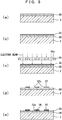
- FIG.1 to FIG.4 show a first embodiment of this invention and FIG.1 is a typical cross-sectional drawing of a semiconductor light emitting element.
- a light emitting element 1 has a semiconductor layer stack part 19 consisting of group-III nitride semiconductor layers, which is formed on a main surface of a sapphire substrate 2 having a diffractive face 2a.
- This light emitting element 1 is face-up type and light is mainly extracted from an opposite side to the sapphire substrate 2.
- the group-III nitride semiconductor layers have a buffer layer 10, an n-type GaN layer 12, a multiple quantum well active layer 14, an electron blocking layer 16 and a p-type GaN layer 18 in this order from the sapphire substrate 2 side.
- a p-side electrode 20 is formed on the p-type GaN layer 18 and an n-side electrode 24 is formed on the n-type GaN layer 12.
- the sapphire substrate 2 has the diffractive face 2a at the main surface side, that is C-face ( ⁇ 0001 ⁇ ) a nitride semiconductor grows.
- a flat part 2b (see FIG.2(a) ) and a plurality of convex portions 2c which are periodically formed in the flat part 2b (see FIG.2(a) ) are formed at the diffractive face 2a.
- a shape of each convex portion 2c can be a cone shape such as a circular cone, polygonal cone etc. or a cone trapezoidal shape such as a circular cone trapezoidal shape, polygonal cone trapezoidal shape etc., which is shaped like cutting upper part of a cone.
- a diffractive effect is obtained by each convex portion 2c which is periodically positioned.
- a reflective film 26 consisting of, for example, Al is formed at a side of the back surface of the sapphire substrate 2.
- a face at the sapphire substrate 2 side of the reflective film 26 is a reflective face 28 and light emitted from the active layer 14 is transmitted through the diffractive face 2a by a diffractive effect and transmitted light is reflected at the reflective face 28.
- light can be extracted in multimode since light which is transmitted by a diffractive effect is incident to the diffractive face 2a and is transmitted through the diffractive face 2a again by a diffractive effect at the diffractive face 2a.
- the buffer layer 10 is formed on the diffractive face 2a of the sapphire substrate 2 and consists of AlN.
- the buffer layer 10 is formed by MOCVD method (Metal Organic Chemical Vapor Deposition) and can be also formed by sputtering method.
- the buffer layer 10 has a plurality of concave portions which have a cone trapezoidal shape and are periodically formed along each convex portion 2c at diffractive face 2a side.
- the n-type GaN layer 12 as a first conductivity type layer is formed on the buffer layer 10 and consists of n-GaN.
- the multiple quantum well active layer 14 as an emitting layer is formed on the n-type layer 12 and consists of GaNInN/GaN.
- the multiple quantum well active layer 14 emits blue light by an injection of electrons and holes.
- blue light is, for example, light having peak wavelength of 430 nm or more to 480 nm or less.
- the multiple quantum well active layer 14 emits at peak wavelength of 450 nm.
- the electron blocking layer 16 is formed on the multiple quantum well active layer 14 and consists of p-AlGaN.
- the p-type GaN layer 18 as a second type conductivity layer is formed on the electron blocking layer 16 and consists of p-GaN. It is formed by an epitaxial growth of group-III nitride semiconductor from the buffer layer 10 to the p-type layer 18.
- the convex portions 2c are periodically formed on the diffractive face 2a of the sapphire substrate 2, it is planarized by a lateral growth in early phase of growing a group-III nitride semiconductor.
- the semiconductor layer constitution is arbitrary if it contains at least a first conductivity layer, an active layer and a second conductivity layer and the active layer emits by recombination of electrons and holes when applying a voltage between the first conductivity layer and the second conductivity layer.
- the p-side electrode 20 is formed on the p-type GaN layer 18 and consists of transparency material such as ITO (Indium Tin Oxide) etc.
- the p-side electrode 20 is formed by a vacuum evaporation method, sputtering method, CVD (Chemical Vapor Deposition) method etc.
- the n-side electrode 24 is formed on the n-type GaN layer 12 exposed by etching the p-type GaN layer 18 to the n-type GaN layer 12.
- the n-side electrode 24 consists of, for example, Ti/Al/Ti/Au and formed by a vacuum evaporation method, sputtering method, CVD (Chemical Vapor Deposition) method etc.
- FIG.2 is drawings of a sapphire substrate, and (a) shows a typical perspective drawing, (b) shows a typical explanation drawing of an A-A cross section and (c) shows a typical magnified drawing.
- the diffractive face 2a is aligned in intersections of hypothetical triangle grid with a predetermined period so that centers of each convex portion 2c are positioned at equilateral triangle vertices.
- the period of each convex portion 2c is longer than an optical wavelength of light emitted from the multiple quantum well active layer 14 and shorter than a coherent length of the light.
- the term "period” means that a distance between peak height positions of adjacent convex portions 2c.
- optical wavelength means that a value actual wavelength is divided by a refraction index.
- coherent length corresponds to a distance coherence disappears by counteracting periodic wave oscillation each other caused by differences of individual wavelength in photon group of predetermined spectrum width.
- the period of each convex portion 2c is 500 nm. Since a wavelength of light emitted from the active layer 14 is 450 nm and a refraction index of a group-III nitride semiconductor is 2.4, the optical wavelength is 187.5 nm. Also, since a half maximum full-width of the light emitted from the active layer 14 is 63 nm, the coherent length of the light is 3214 nm. The period of the diffractive face 2a is longer than twice the optical wavelength of light emitted from the active layer 14 and equal to or shorter than a half of the coherent length of the light.
- each convex portion 2c of the diffractive face 2a has a side surface 2d which extends upward from the flat part 2b, a curved portion 2e which curves and extends to center side of the convex portion 2c from the upper end of the side surface 2d and an upper surface 2f which is flat and is continuously formed from the curved portion 2e.
- the curved portion 2e is formed by rounding off the corner by wet-etching the convex portion 2c (see FIG.4(e) ) which is formed a corner made by the side surface 2d and the upper surface 2f before forming the curved portion 2e.
- each convex portion 2c has a base end section whose diameter is 200 nm, and the height of each convex portion 2c is 250 nm.
- the diffractive face 2a of the sapphire substrate 2 is the flat part 2b except each convex portion 2c and a lateral growth of semiconductor layer is assisted.
- FIG.3 is an explanation drawing for processing a sapphire substrate, and (a) shows a substrate that a first mask layer is formed on a diffractive face, (b) shows a substrate that a resist layer is formed on a first mask layer, (c) shows a substrate that an electron beam is selectively irradiated to a resist layer, (d) shows a substrate that a resist mask is developed and removed, (e) shows a substrate that a second mask layer is formed.
- a sapphire substrate 2 shaped like a flat plate is prepared and a first mask layer 30 is formed on the main surface of the sapphire substrate 2.
- the first mask layer 30 consists of, for example, SiO 2 and formed by a sputtering method, vacuum evaporation method, CVD method etc.
- the thickness of the first mask layer 30 is arbitrary and, for example, it is 1.0 ⁇ m.
- a resist layer 32 is formed on the first mask layer 30 of the sapphire substrate 2.
- the resist layer 32 consists of, for example, electron beam sensitive material of ZPE etc. manufactured by Japan Zeon Corporation and is applied on first mask layer 30.
- the thickness of the resist layer 32 is arbitrary and, for example, 100 nm to 2.0 ⁇ m.
- a stencil mask 34 is set with a clearance from the resist mask 32.
- the clearance between the resist mask 32 and the stencil mask 34 is 1.0 ⁇ m to 100 ⁇ m.
- the stencil mask 34 consists of, for example, material such as diamond, SiC etc.
- the thickness of the stencil mask 34 is arbitrary and, for example, 500 nm - 100 ⁇ m.
- the stencil mask 34 has apertures 34a that an electron beam transmits selectively.
- an electron beam is irradiated to the stencil mask 34 and the resist layer 32 is exposed to an electron beam transmitting the apertures 34a of the stencil mask 34.
- a pattern of the stencil mask 34 is printed to the resist layer 32, for example, by using an electron beam of 10 - 100 ⁇ C/cm 2 .
- the resist layer 32 is developed by using predetermined developing fluid.
- a part that an electron beam irradiated is eluted in the developing fluid and a part that an electron beam did not irradiate stays, thus, apertures 32a are formed.
- amyl acetate can be used as the developing fluid.
- a second mask layer 36 is formed on the first mask layer 30 that the resist layer 32 is patterned.
- the second mask layer 32 is patterned on the first mask layer 30 by electron beam irradiation.
- the second mask layer 36 consists of, for example, Ni and formed by a sputtering method, vacuum evaporation method, CVD method etc.
- the thickness of the second mask layer 36 is arbitrary and, for example, it is 20 nm.
- FIG.4 is an explanation drawing for processing a sapphire substrate, and (a) shows a substrate that a resist layer is completely removed, (b) shows a substrate that a first layer is etched by using a second mask layer as a mask, (c) shows a substrate that a second mask layer is removed, (d) shows a substrate that a diffractive face etched by using a first mask layer as a mask, (e) shows a substrate that a first mask layer is removed and (f) shows a substrate that a curved portion is provided at a convex portion by wet etching.
- the resist layer 32 is removed by using parting agent.
- parting agent for example, it can be removed in condition that the resist layer 32 is soused in the parting agent and ultrasonic wave is irradiated for predetermined time.
- diethyl ketone can be used as parting agent.
- a pattern of the second mask layer 36 that has a shape the pattern of apertures 34a of the stencil mask 34 is inverted is formed on the first mask layer 30.
- the first mask layer 30 is dry-etched by using the second mask layer 36 as a mask, In this way, apertures 30a are formed in the first mask layer 30 and a pattern of the first mask layer 30 is formed.
- etching gas having a tolerance that the sapphire substrate 2 and the first mask layer 30 are larger than the second mask layer 36 is used.
- the first mask layer 30 is SiO 2 and the second mask layer 36 is Ni
- fluorine series gas is used, the pattern of the first mask layer 30 can be formed with precision since Ni has etching selectivity of about 100 to SiO 2 .
- the second mask layer 36 on the first mask layer 30 is removed.
- the first mask layer 30 is SiO 2 and the second mask layer 36 is Ni
- Ni can be removed by sousing in hydrochloric acid and nitric acid which are mixed in a ratio 1:1 and diluted with water or dry-etching using argon gas.
- the sapphire substrate 2 is dry-etched by using the first mask layer 30 as a mask.
- a reverse pattern of apertures 34a of the stencil mask 34 is transcribed on the sapphire substrate 2, since only a part that the first mask layer 30 is removed in the sapphire substrate 2 is exposed to etching gas.
- a part which is not covered by the first mask layer 30 can be etched selectively since the first mask layer 30 has a larger tolerance to the etching gas than the sapphire substrate 2.
- the etching is finished when an etching depth of the sapphire substrate 2 reaches the predetermined depth.
- chlorine series gas such as BCl 3 etc. is used as the etching gas.
- the first mask layer 30 left on the sapphire substrate 2 is removed by using predetermined parting agent.
- the convex portion 2c which is formed a corner made by the side surface 2d and the upper surface 2f before forming the curved portion 2e is formed.
- the first mask layer 30 is SiO 2
- dilute hydrofluoric acid can be used as parting agent.
- the curved portion 2e is formed by rounding off the corner by wet-etching the convex portion 2c.
- etchant is arbitrary, for example, phosphoric acid aqueous solution heated to about 160 °C, called “hot phosphoric acid” can be used.
- Other methods such as dry-etching can be used as an etching method and the point is to form the curved portion 2e to the corner of convex portion 2c.
- a group-III nitride semiconductor is epitaxially grown by using a lateral growth on the diffractive face 2a of the sapphire substrate 2 as made above and the light emitting element 1 is manufactured by dividing to a plurality of the light emitting element 1 by dicing after forming each electrode.
- incident light having an angle over the total reflection optimal angle at the interface of the sapphire substrate 2 and the group-III nitride semiconductor can be extracted to the outside of element by using a diffractive effect since it comprises the diffractive face 2a having the convex portions 2c that the period is longer than the optical wavelength of light emitted from the multiple quantum well active layer 14 and shorter than the coherent length of the light, and the reflective face 28 which reflects light diffracted at the diffractive face 2a and let the reflected light be incident to the diffractive face 2a again.
- light can be extracted in multimode since light which is transmitted by a diffractive effect is incident to the diffractive face 2a and is transmitted through the diffractive face 2a again by a diffractive effect at the diffractive face 2a.
- a diffractive effect since light is extracted by a diffractive effect, a different effect from the one that light is extracted by scattering effect is obtained and a light extraction efficiency of the light emitting element 1 can be highly improved.
- the number of convex portions 2c per unit area increases since the convex portion 2c is formed in a short period.
- the period of the convex portion 2c exceeds twice the coherent length, if the convex portion 2c has a corner dislocations originate, the emission efficiency is not influenced since the dislocation density is small.
- the period of the convex portion 2c is shorter than the coherent length, the emission efficiency highly decreases since the dislocation density in the buffer layer 10 of the semiconductor layer stack part 19 increases. If the period is equal to or lower than 1 ⁇ m, this tendency highly increases. This is a new problem in case that the period of convex portion 2c is equal to or lower the coherent length.
- the convex portions 2c are formed on the diffractive face 2a of the sapphire substrate 2, since an end of dislocations is generated when a group-III nitride semiconductor is planarized by a lateral growth, crystal which has a relatively low dislocation density is obtained in the group-III nitride semiconductor. As a result, crystal has a relatively low dislocation density in the multiple quantum well active layer 14 and the emission efficiency does not decrease by forming the convex portion 2c at the diffractive face 2a.
- the light emitting element 1 is face-up type, for example, as shown in FIG.5
- the light emitting element 1 can be flip-chip type.
- the light emitting element 1 in FIG.5 has a buffer layer 10, an n-type GaN layer 12, a multiple quantum well active layer 14, an electron blocking layer 16 and a p-type GaN layer 18 in this order on the sapphire substrate 2, and a p-side electrode 20 consisting of reflective material such as Ag system, Rh system etc. is formed on the p-type GaN layer 18 and n-side electrode 24 is formed on the n-type GaN layer 12.
- a surface of the p-type GaN layer 18 of the p-side electrode 20 is a reflective face 22.
- a second diffractive face 20a can be formed at a surface of the p-side electrode 20. It is desirable that this concavo-convex period of the diffractive face 20a is also shorter than the coherent length of light emitted from the multiple quantum well active layer 14. In this way, both of diffractive effects can be obtained at the diffractive face 2a of the sapphire substrate 2 and the diffractive face 20a of the p-side electrode 20.
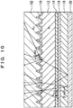
- FIG.7 to FIG.16 show a second embodiment of this invention and FIG.7 is a typical cross-sectional drawing of a semiconductor light emitting element.
- a light emitting element 100 has a semiconductor layer stack part 119 consisting of group-III nitride semiconductor layers, which is formed on a sapphire substrate 102 having a diffractive face 102a.
- This light emitting element 100 is flip-chip type and light is mainly extracted from a back surface (an upper surface in FIG.7 ) of the sapphire substrate 102.
- the group-III nitride semiconductor layers have a buffer layer 110, an n-type GaN layer 112, a multiple quantum well active layer 114, an electron blocking layer 116 and a p-type GaN layer 118 in this order from the sapphire substrate 102 side.
- a p-side electrode 120 is formed on the p-type GaN layer 118 and an n-side electrode 124 is formed on the n-type GaN layer 112.
- the sapphire substrate 102 has the diffractive face 102a that is C-face ( ⁇ 0001 ⁇ ) a nitride semiconductor grows.
- a flat part 102b and a plurality of concave portions 102c which are a cone shape and periodically formed in the flat part 102b are formed at the diffractive surface 102a.
- a shape of each concave portion 102c can be a circular cone, polygonal cone etc.
- diffractive effect is obtained by each concave portion 102c which is periodically positioned.
- the buffer layer 110 is formed on the diffractive face 102a of the sapphire substrate 102 and consists of GaN. In this embodiment, the buffer layer 110 is grown at lower temperature than the n-type GaN layer 112 etc. described below.
- the buffer layer 110 has a plurality of convex portions which have a cone shape and are periodically formed along each concave portion 102c at diffractive face 102a side.
- the n-type GaN layer 112 as a first conductivity type layer is formed on the buffer layer 110 and consists of n-GaN.
- the multiple quantum well active layer 114 as an emitting layer is formed on the n-type layer 112 and consists of GaNInN/GaN and emits blue light by an injection of electrons and holes. In this document, blue light is, for example, light having peak wavelength of 430 nm or more to 480 nm or less. In this embodiment, the multiple quantum well active layer 114 emits at peak wavelength of 450 nm.
- the electron blocking layer 116 is formed on the multiple quantum well active layer 114 and consists of p-AlGaN.
- the p-type GaN layer 118 as a second type conductivity layer is formed on the electron blocking layer 116 and consists of p-GaN. It is formed by an epitaxial growth of group-III nitride semiconductor from the buffer layer 110 to the p-type layer 118. Although the concave portions 102c are periodically formed on the diffractive face 102a of the sapphire substrate 102, it is planarized by a lateral growth in early phase of growing group-III nitride semiconductor.
- the semiconductor layer constitution is arbitrary if it contains at least a first conductivity layer, an active layer and a second conductivity layer and the active layer emits by recombination of electrons and holes when applying a voltage between the first conductivity layer and the second conductivity layer.
- the p-side electrode 120 is formed on the p-type GaN layer 118, that a p-type GaN layer 118 side face is a reflective face 122.
- the p-side electrode 120 has high reflection rate of light emitted from the multiple quantum well active layer 114. It is preferable that the p-side electrode 120 has 80 % of reflection rate of light emitted from the multiple quantum well active layer 114.
- the p-side electrode 120 consists of, for example, material of Ag system, Rh system etc. and is formed by a vacuum evaporation method, sputtering method, CVD (Chemical Vapor Deposition) method etc.
- the n-side electrode 124 is formed on the n-type GaN layer 112 exposed by etching the p-type GaN layer 118 to the n-type GaN layer 112.
- the n-side electrode 124 consists of, for example, Ti/Al/Ti/Au and formed by a vacuum evaporation method, sputtering method, CVD (Chemical Vapor Deposition) method etc.
- FIG.8 is drawings of a sapphire substrate, and (a) shows a typical perspective drawing and (b) shows a typical explanation drawing of a B-B cross section.
- the diffractive face 102a is aligned in intersections of hypothetical triangle grid with a predetermined period so that centers of each concave portion 102c are positioned at equilateral triangle vertices.
- the period of each concave portion 102c is longer than the optical wavelength of light emitted from the multiple quantum well active layer 114 and shorter than the coherent length of the light.
- the term "period” means that a distance between peak depth positions of adjacent concave portions 102c.
- optical wavelength means that a value actual wavelength is divided by a refraction index.
- coherent length corresponds to a distance coherence disappears by counteracting periodic wave oscillation each other caused by differences of individual wavelength in photon group of predetermined spectrum width.
- the period of each concave portion 102c is 500 nm. Since a wavelength of light emitted from the active layer 114 is 450 nm and a refraction index of group-III nitride semiconductor is 2.4, the optical wavelength is 187.5 nm. Also, since a half maximum full-width of the light emitted from the active layer 114 is 63 nm, the coherent length of the light is 3214 nm. The period of the diffractive face 102a is longer than twice the optical wavelength of light emitted from the active layer 114 and equal to or shorter than a half of the coherent length of the light.
- each concave portion 102c of the diffractive face 102a is formed in a circular cone shape.
- each concave portion 102c has a base end section whose diameter is 200 nm, and the depth of each concave portion 102c is 250 nm.
- the diffractive face 102a of the sapphire substrate 102 is the flat part 102b except each concave portion 102c and a lateral growth of semiconductor layer is assisted.
- FIG.9 is an explanation drawing of a diffractive effect of light at an interface of different refractive indices, and (a) shows reflected light at an interface and (b) shows transmitted light at an interface.
- n1 is refraction index of incident side medium
- ⁇ is a wavelength of incident light
- m is an integer.
- n1 is refraction index of group-III nitride semiconductor.
- n2 is refraction index of output side medium and m' is an integer.
- n2 is refraction index of the sapphire substrate 2.
- the period of the diffractive face 102a should be longer than ( ⁇ /n1) and ( ⁇ /n2) which are the optical wavelength of inside of an element.
- a well known moth-eye structure is designed that a period is shorter than ( ⁇ /n1) and ( ⁇ /n2) and diffractive light does not exist.
- the period of diffractive face 102a should be shorter than the coherent length that light keep the wave nature and is preferable to be equal to or less than a half of the coherent length. The light being equal to or less than a half of the coherent length secures the strength of reflection light and transmission light by diffractive effect.
- FIG.10 is an explanation drawing of a diffractive effect of light being incident to a sapphire substrate from a group-III nitride semiconductor.
- light being incident to the sapphire substrate 102 at the incident angle ⁇ in of light isotopic radiated from the multiple quantum well active layer 114 in the light emitting element 100, is reflected at the reflection angle ⁇ ref which meets the above formula (1) and is transmitted at the transmission angle ⁇ out which meets the above formula (2).
- the incident angle ⁇ in is equal to or more than the total reflection optimal angle, the strength of reflection light is larger.
- the reflection light is reflected at the reflection face 122 of the p-side electrode 120 and is incident to the moth-eye face 102a again.
- the reflection light since the reflection light is incident at a different angle from the former incident angle ⁇ in , the reflection light has a different transmission property from the former incident condition
- FIG.11 is a graph showing a relationship between an incident angle of light being incident to an interface from semiconductor layer side and a reflecting angle of light at an interface by a diffractive face, at an interface of a group-III nitride semiconductor and a sapphire substrate in case that a period of concave portions or convex portions is 500 nm.
- the total reflection optimal angle exists as well as a general flat face.
- the optimal angle is about 45 degree at an interface of GaN system semiconductor layer and the sapphire substrate 102.
- FIG.12 is a graph showing a relationship between an incident angle of light being incident to an interface from semiconductor layer side and a transmission angle of light at an interface by a diffractive surface, at an interface between a group-III nitride semiconductor and a sapphire substrate in case that a period of concave portions or convex portions is 500 nm.
- FIG.13 is a graph showing a relationship between an incident angle of light entering an interface from semiconductor layer side for the first time and a transmission angle of light being incident to for the second time after reflected by a diffraction effect, at an interface by a diffractive face, at an interface of a group-III nitride semiconductor and a sapphire substrate in case that a period of concave portions or convex portions is 500 nm.
- the mode index l about transmission of light being incident for the second time has the same transmission property as long as the mode index l is same, if the mode index m about reflection for the first incident time and the mode index m' about transmission for the second incident time are any value.
- incident light having an angle over the total reflection optimal angle at the interface of the sapphire substrate 102 and a group-III nitride semiconductor can be extracted to the outside of element by using a diffractive effect since it comprises the diffractive face 102a having the concave portions 102c that the period is longer than the optical wavelength of light emitted from the multiple quantum well active layer 114 and shorter than the coherent length of the light, and the reflective face 120 which reflects light diffracted at the diffractive face 102a and let the reflected light be incident to the diffractive face 102a again.
- a diffractive effect since light is extracted by a diffractive effect, a different effect from the one that light is extracted by scattering effect is obtained and a light extraction efficiency of the light emitting element 100 can be highly improved.
- the active layer 114 as a light emitting layer is sandwiched between the diffractive face 102a and the reflective face 120, the reflective angle ⁇ ref different from the incident angle ⁇ in at the diffractive face 102a can be incident at the former incident angle ⁇ in .
- the diffractive face 102a since light is incident to the diffractive face 102a in different condition for the first time and second condition, many transmission modes exist and it has an advantage in the light extraction.
- refractive index of group-III nitride semiconductor is 2.4 and refractive index of sapphire is 1.8, thus, the diffractive face 102a is formed at an interface of materials whose refractive index difference is equal to or more than 0.5. If refractive index difference is equal to or more than 0.5, the light extraction is relatively disadvantageous. However, light can be adequately extracted from the light emitting element 100, it has an advantage in actual use.
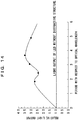
- FIG.14 is a graph showing a relationship between a period of a diffractive face and a relative light output in case that an optical wavelength is 258 nm and a diffractive face is provided at an interface of a sapphire substrate and group-III nitride semiconductor layer.
- an output that an interface of a sapphire substrate and group-III nitride semiconductor layer is a flat face is 1.0.
- data are obtained by applying an electrical current to a chip of 1.0 mm squares at room temperature in a condition with a distance of the active layer to the diffractive face is 3.0 ⁇ m and a distance of the diffractive face to the back side of the sapphire substrate is 100 ⁇ m. Also, one amount of the relative light output corresponds to 40 mW.
- a light extraction efficiency increases by suppressing Fresnel reflection at an angle which is equal to or less than the total the total reflection optimal angle.
- a light extraction efficiency increases since both a diffraction effect and a suppressing Fresnel reflection effect can be obtained.
- a light extraction efficiency slightly decreases since a suppressing Fresnel reflection effect disappears.
- a light extraction efficiency increases again since incident light which meets the diffraction condition increases.
- a light extraction efficiency increases again since incident light which meets the diffraction condition increases.
- a light extraction efficiency is equal to or more than three times of the optical wavelength and is equal to or less than five times of the optical wavelength.
- FIG.14 illustrates up to about six times of the optical wavelength concerning the period
- the light output is about twice the output of a flat face when the period is a half of the coherent length and the light output is about 1.8 times output of a flat face when the period is equal to the coherent length.
- the reason why the output is larger than a flat face even in the coherent length is to be able to obtain a scattering effect by concave portions or convex portions. In this way, a diffractive effect can be obtained when the period exceeds one amount of the optical wavelength and it is understood that the light output of the light emitting element 100 highly increases when exceeding two-and-a-half times of the optical wavelength.
- FIG.15 is an explanation drawing for processing a sapphire substrate, and (a) shows a substrate that a first mask layer is formed on a diffractive surface, (b) shows a substrate that a resist layer is formed on a first mask layer, (c) shows a substrate that an electron beam is selectively irradiated to a resist layer, (d) shows a substrate that a resist mask is developed and removed, (e) shows a substrate that a second mask layer is formed.
- a sapphire substrate 102 shaped like a flat plate is prepared and a first mask layer 130 is formed on the main surface of the sapphire substrate 102.
- the first mask layer 130 consists of, for example, SiO 2 and formed by a sputtering method, vacuum evaporation method, CVD method etc.
- the thickness of the first mask layer 130 is arbitrary and, for example, it is 1.0 ⁇ m.
- the first mask layer 130 is formed by a magnetron sputtering system
- Ar gas and highfrequency (RF) power source can be used.
- the first mask layer 130 of 600 nm can be formed in condition that Ar gas is 25 sccm and the power of the RF power source is 200-500 W in accordance with material.
- Sputtering time can be arbitrary adjusted at that time.
- a resist layer 132 is formed on the first mask layer 130 of the sapphire substrate 102.
- the resist layer 132 consists of, for example, electron beam sensitive material of ZPE etc. manufactured by Japan Zeon Corporation and is applied on first mask layer 130.
- the thickness of the resist layer 132 is arbitrary and, for example, 100 nm to 2.0 ⁇ m.
- the resist mask layer 132 of thickness of 160-170 nm can be obtained by baking for four minutes at 180 °C after an uniform thickness film is formed in condition with rotating speed of spinner of 1500 rpm.
- ZPE manufactured by Japan Zeon Corporation and diluting fluid of ZEP-A manufactured by Japan Zeon Corporation which are mixed in a ratio 1:1.4 can be uses as material of the resist layer 132.
- a stencil mask 134 is set with a clearance from the resist mask 132.
- the clearance between the resist mask 132 and the stencil mask 134 is 1.0 ⁇ m to 100 ⁇ m.
- the stencil mask 134 consists of, for example, material such as diamond, SiC etc.
- the thickness of the stencil mask 134 is arbitrary and, for example, 500 nm to 100 ⁇ m.
- the stencil mask 134 has apertures 134a that electron beam transmits selectively.
- the stencil mask 134 is formed a thin plate shape having constant thickness and it is possible that the thickness is partially thick, for example, by providing a lattice-shaped or line-shaped thick part in order of giving a strength.
- concave portions 102c which correspond to a plurality of the light emitting element 100 is formed on sapphire substrate 102 shaped a wafer and a plurality of the light emitting elements 100 are manufactured by dicing it after an epitaxial growth of group-III nitride semiconductor.
- the thick part of the stencil mask 134 can be formed in corresponding a passing position of a dicing blade.
- the thick part may project to sapphire substrate 102 side, opposite side of the sapphire substrate 102, or both sides. In case of projecting to the sapphire substrate 102 side, contacting a top edge of the thick part to the resist layer 132 gives spacer function to the thick part.
- an electron beam is irradiated to the stencil mask 134 and the resist layer 132 is exposed to an electron beam transmitting the apertures 134a of the stencil mask 134.
- a pattern of the stencil mask 134 is printed to the resist layer 132, for example, by using an electron beam of 10 - 100 ⁇ C/cm 2 .
- An electron beam is irradiated a spot shape to the stencil mask 134 and, in actuality by scanning an electron beam, an electron beam is irradiated to a whole surface of the stencil mask 134.
- the resist layer 132 is positive type and solubility to developing solution increases when exposed.
- the resist layer 132 may be negative type.
- volatilization components are easy to diffuse by the clearance between the resist layer 132 and the stencil mask 134 and it is prevented that the stencil mask 134 is polluted by the volatilization components.
- the resist layer 132 is developed by using predetermined developing fluid. In this way, as shown in FIG.15(d) , a part that an electron beam irradiated is eluted in the developing fluid and a part that an electron beam did not irradiate stays, thus, apertures 132a are formed.
- ZPE manufactured by Japan Zeon Corporation for example, amyl acetate can be used as the developing fluid.
- IPA isopropyl alcohol
- a second mask layer 136 is formed on the first mask layer 130 that the resist layer 132 is patterned.
- the second mask layer 132 is patterned on the first mask layer 130 by electron beam irradiation.
- the second mask layer 136 consists of, for example, Ni and formed by a sputtering method, vacuum evaporation method, CVD method etc.
- the thickness of the second mask layer 136 is arbitrary and, for example, it is 20 nm.
- the second mask layer can be formed by, for example, a magnetron sputtering system as well as the first mask layer.
- FIG.16 is an explanation drawing for processing a sapphire substrate, and (a) shows a substrate that a resist layer is completely removed, (b) shows a substrate that a first layer is etched by using a second mask layer as a mask, (c) shows a substrate that a second mask layer is removed, (d) shows a substrate that a diffractive face etched by using a first mask layer as a mask and (e) shows a substrate that a first mask layer is removed.
- the resist layer 132 is removed by using parting agent.
- parting agent for example, it can be removed in condition that the resist layer 132 is soused in the parting agent and ultrasonic wave is irradiated for predetermined time.
- diethyl ketone can be used as parting agent.
- rinse fluid for example, acetone, methanol etc.
- the first mask layer 130 is dry-etched by using the second mask layer 136 as a mask, In this way, apertures 130a are formed in the first mask layer 130 and a pattern of the first mask layer 130 is formed.
- etching gas having tolerance that the sapphire substrate 102 and the first mask layer 130 are larger than the second mask layer 136 is used.
- the first mask layer 130 is SiO 2 and the second mask layer 136 is Ni
- fluorine series gas is used, the pattern of the first mask layer 130 can be formed with precision since Ni has etching selectivity of about 100 to SiO 2 .
- the second mask layer 136 on the first mask layer 130 is removed.
- the first mask layer 130 is SiO 2 and the second mask layer 136 is Ni
- Ni can be removed by sousing in hydrochloric acid and nitric acid which are mixed in a ratio 1:1 and diluted with water or dry-etching using argon gas.
- the sapphire substrate 102 is dry-etched by using the first mask layer 130 as a mask.
- a reverse pattern of apertures 134a of the stencil mask 134 is transcribed on the sapphire substrate 102, since only a part that the first mask layer 130 is removed in the sapphire substrate 102 is exposed to etching gas.
- a part which is not covered by the first mask layer 130 can be etched selectively since the first mask layer 130 has larger tolerance to the etching gas than the sapphire substrate 102.
- the etching is finished when an etching depth of the sapphire substrate 102 reaches the predetermined depth.
- the concave portion 102c having a circular cone shape that the diameter of the base end section is 150 nm is finally formed.
- contact points of the first mask layer 130 and the sapphire substrate 102 is lost with progression of etching and the first mask layer 130 is removed from an outside edge.
- chlorine series gas such as BCl 3 etc. is used as the etching gas.
- a reverse pattern of apertures 134a of the stencil mask 134 is designed so that the shape is same as the base end section of each concave portion 102c.
- the first mask layer 130 left on the sapphire substrate 102 is removed by using predetermined parting agent.
- predetermined parting agent for example, in case that the first mask layer 130 is SiO 2 , dilute hydrofluoric acid can be used as parting agent.
- a group-III nitride semiconductor is epitaxially grown by using a lateral growth on the diffractive face 102a of the sapphire substrate 102 as made above and the light emitting element 100 is manufactured by dividing to a plurality of the light emitting element 100 by dicing after forming each electrode.
- the concave portions 102c are formed on the diffractive face 102a of the sapphire substrate 102, since an end of dislocations is generated when the group-III nitride semiconductor is planarized by a lateral growth, crystal which has a relatively low dislocation density is obtained in the group-III nitride semiconductor. As a result, crystal has a relatively low dislocation density in the multiple quantum well active layer 114 and the emission efficiency does not decrease by forming the concave portion 102c at the diffractive face 102a.
- the light emitting wavelength of the active layer 114 and the period of the diffractive face 102a in the above embodiment are arbitrary, in case that the active layer 114 emits blue light, a high light extraction efficiency can be obtained when the period of the diffractive face 102a is equal to or more than 300 nm and equal to or less than 1500 nm.
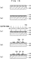
- the light emitting element 100 is flip-chip type, for example, as shown in FIG.17 , the light emitting element 100 can be face-up type.
- the light emitting element 200 in FIG.17 has a buffer layer 210, an n-type GaN layer 212, a multiple quantum well active layer 214, an electron blocking layer 216 and a p-type GaN layer 218 in this order on the sapphire substrate 202, and a p-side transparent electrode 220 consisting of, for example, ITO (Indium Tin Oxide) is formed on the p-type GaN layer 218 and n-side electrode 224 is formed on the n-type GaN layer 212.
- ITO Indium Tin Oxide
- a reflective film 226 consisting of, for example, Al is formed on the back side of the sapphire substrate 202.
- a face at the sapphire substrate 200 side of the reflective film 226 is a reflective face 228 and light emitted from the active layer 214 is transmitted through the diffractive face 202a by a diffractive effect and transmitted light is reflected at the reflective face 228.
- light can be extracted in multimode since light which is transmitted by a diffractive effect is incident to the diffractive face 202a and is transmitted through the diffractive face 202a again by a diffractive effect at the diffractive face 202a.
- the diffractive face 102a is formed at an interface of the sapphire substrate 102 and group-III nitride semiconductor, for example, as shown in FIG.18 , a diffractive face 312a can be formed at a surface of light emitting element 300.
- the light emitting element 300 is a thin-film-type light emitting diode and has a p-side electrode 320, a p-type GaN layer 318, an electron blocking layer 316, a multiple quantum well active layer 314 and an n-type GaN layer 312 in this order on a conductive substrate 302.
- a n-type electrode 324 is formed on the center of the surface of the n-type GaN layer 312 and a part of not forming the n-type electrode 324 on the n-type GaN layer 312 is a surface of element and the diffractive face 312a is formed on this part.
- the diffractive face 312a and the reflective face 322 of the p-side electrode 320 are arranged opposite side sandwiching the active layer 314.
- the diffractive face 312a which is an interface of the n-type GaN layer 312 and medium of outside of element and a diffractive effect can be obtained at this interface.
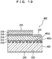
- a plurality of concave portions 102c are formed at the diffractive face 102a, for example, as shown in FIG.19 , a plurality of convex portions 402c can be formed at the diffractive face 402a of the sapphire substrate 402.
- the light emitting element 400 in FIG.19 that the diffractive face 402a of the light emitting element 200 in FIG.17 is modified has convex portions 402c which are aligned in intersections of hypothetical square grid with a predetermined period.
- concave portions or convex portions can be formed a polygonal cone such as a triangular cone or square cone, and other concrete detail structures can be changed arbitrarily
- the semiconductor light emitting element of the present invention increases the light extraction efficiency, it is useful industrially.
Abstract
[PROBLEM] A light extraction efficiency increases by suppressing a reflection of a semiconductor layer and a transparent substrate.
[MEANS FOR SOLVING] A semiconductor light emitting element comprising a semiconductor stack (19) part including a light emitting layer, a diffractive face (2a) that light emitted from the light emitting layer is incident to, that convex portions (2c) are formed in a period which is longer than optical wavelength of the light and is shorter than coherent length of the light, and a reflective face which reflects light diffracted at the diffractive face and let this light be incident to the diffractive face again. The convex portions (2c) have a flat upper surface (2f) which is parallel to the main surface side.
Description
- The present invention relates to a semiconductor light emitting element.
- High brightness light emitting diodes such as blue, green, white etc. are already put to practical use by the accumulation of essential technology such as cold deposited buffer layer technology, p-type conductivity control, n-type conductivity control, high efficiency emitting layer etc. In an existing light emitting diode, to increase the light extraction is the problem since refractive index of semiconductor is larger than refractive index of air etc. and, thus, most of light can not be taken off to the outside of the light emitting diode by total reflection or Fresnel reflection.
- For solving this problem, a concavo-convex structure which is worked on the semiconductor surface in several micrometer period is proposed (for example, see the non-patent literature 1). When a concavo-convex structure is provided at an extraction side of the semiconductor surface, the total reflection is lost by the light scattering effect and about 50 % transmission can be obtained in the relatively wide radiation angle, thus, the light extraction efficiency can be improved to about 50 %.
- Also, to increase the light extraction by providing the period of the concavo-convex structure which is equal to or smaller than twice the optical wavelength is proposed(for example, see the patent literature 1). In this case, the mechanism for extracting light differs from the period of several micrometer of the concavo-convex structure. Wave nature of light appears and the border of reflective index disappears, and thus, Fresnel reflection is suppressed. Such structure is called photonic crystal or moth-eye structure and can increase the light extraction up to about 50 %.
- PATENT LITERATURE 1: Japanese Unexamined Patent Application Publication No.
2005-354020 -
JP 2009 123717 A1 JP 2009 123717 A1 -
US 2008/0303047 A1 describes a light emitting diode device with a pattern micro-lens substrate. A reflector layer is formed on the lower surface of the micro-lens substrate. - NON-PATENT LITERATURE 1: Japanese Journal of Applied Physics Vol.41, 2004, L1431
- However, the increase of the light extraction in the
patent literature 1 and thenon-patent literature 1 is limited and a further increase of the efficiency is desired. - The present invention has been achieved in view of the above-mentioned background, thus, an object of the present invention is to provide a semiconductor light emitting element which can increase the light extraction efficiency.
- In order to achieve the above purpose, in the present invention, a semiconductor light emitting element comprising a semiconductor stack part including a light emitting layer is formed on a main surface of a substrate, a diffractive face that light emitted from the light emitting layer is incident to, that convex portions or concave portions are formed in a period which is longer than an optical wavelength of the light and is shorter than a coherent length of the light, is formed on a main surface side of the substrate, and a reflective face which reflects light diffracted at the diffractive face and let this light be incident to the diffractive face again is formed on a back surface side of the substrate is provided.
- In the above semiconductor light emitting element, the period of convex portions or concave portions may be longer than twice optical wavelength.
- In the above semiconductor light emitting element, the period of convex portions or concave portions is equals to or less than a half of the coherent length.
- In the above semiconductor light emitting element, the light emitting layer may emit blue light and the period may be equals to or more than 300 nm and may be equals to or less than 1500 nm.
- In the above semiconductor light emitting element, the diffractive face may be provided at an interface of materials whose diffractive index difference is equals to or more than 0.5.
- According to the semiconductor light emitting element of the present invention, it can increase the light extraction efficiency.
-
-
FIG.1 is a typical cross-sectional drawing of a semiconductor light emitting element of a first embodiment of this invention. -
FIG.2 is drawings of a sapphire substrate, and (a) shows a typical perspective drawing, (b) shows a typical explanation drawing of an A-A cross section and (c) shows a typical magnified drawing. -
FIG.3 is an explanation drawing for processing a sapphire substrate, and (a) shows a substrate that a first mask layer is formed on a diffractive face, (b) shows a substrate that a resist layer is formed on a first mask layer, (c) shows a substrate that an electron beam is selectively irradiated to a resist layer, (d) shows a substrate that a resist mask is developed and removed, (e) shows a substrate that a second mask layer is formed. -
FIG.4 is an explanation drawing for processing a sapphire substrate, and (a) shows a substrate that a resist layer is completely removed, (b) shows a substrate that a first layer is etched by using a second mask layer as a mask, (c) shows a substrate that a second mask layer is removed, (d) shows a substrate that a diffractive face etched by using a first mask layer as a mask, (e) shows a substrate that a first mask layer is removed and (f) shows a substrate that a curved portion is provided at a convex portion by wet etching. -
FIG.5 is a typical cross-sectional drawing of a semiconductor light emitting element of an other embodiment of this invention. -
FIG.6 is a typical cross-sectional drawing of a semiconductor light emitting element of an other embodiment of this invention. -
FIG.7 is a typical cross-sectional drawing of a semiconductor light emitting element of a second embodiment of this invention. -
FIG.8 is drawings of a sapphire substrate, and (a) shows a typical perspective drawing and (b) shows a typical explanation drawing of a B-B cross section. -
FIG.9 is an explanation drawing of a diffractive effect of light at an interface of different refractive indices, and (a) shows reflected light at an interface and (b) shows transmitted light at an interface. -
FIG.10 is an explanation drawing of a diffractive effect of light being incident to a sapphire substrate from a group-III nitride semiconductor. -
FIG.11 is a graph showing a relationship between an incident angle of light being incident to an interface from semiconductor layer side and a reflecting angle of light at an interface by a diffractive face, at an interface of a group-III nitride semiconductor and a sapphire substrate in case that a period of concave portions or convex portions is 500 nm. -
FIG.12 is a graph showing a relationship between an incident angle of light being incident to an interface from semiconductor layer side and a transmission angle of light at an interface by a diffractive surface, at an interface between a group-III nitride semiconductor and a sapphire substrate in case that a period of concave portions or convex portions is 500 nm. -
FIG.13 is a graph showing a relationship between an incident angle of light entering an interface from semiconductor layer side for the first time and a transmission angle of light being incident to for the second time after reflected by a diffraction effect, at an interface by a diffractive face, at an interface of a group-III nitride semiconductor and a sapphire substrate in case that a period of concave portions or convex portions is 500 nm. -
FIG.14 is a graph showing a relationship between a period of a diffractive face and a relative light output in case that an optical wavelength is 258 nm and a diffractive face is provided at an interface of a sapphire substrate and group-III nitride semiconductor layer. -
FIG.15 is an explanation drawing for processing a sapphire substrate, and (a) shows a substrate that a first mask layer is formed on a diffractive surface, (b) shows a substrate that a resist layer is formed on a first mask layer, (c) shows a substrate that an electron beam is selectively irradiated to a resist layer, (d) shows a substrate that a resist mask is developed and removed, (e) shows a substrate that a second mask layer is formed. -
FIG.16 is an explanation drawing for processing a sapphire substrate, and (a) shows a substrate that a resist layer is completely removed, (b) shows a substrate that a first layer is etched by using a second mask layer as a mask, (c) shows a substrate that a second mask layer is removed, (d) shows a substrate that a diffractive face etched by using a first mask layer as a mask and (e) shows a substrate that a first mask layer is removed. -
FIG.17 is a typical cross-sectional drawing of a semiconductor light emitting diode element of an other embodiment of this invention. -
FIG.18 is a typical cross-sectional drawing of a semiconductor light emitting diode element of an other embodiment of this invention. -
FIG.19 is a typical cross-sectional drawing of a semiconductor light emitting diode element of an other embodiment of this invention. -
FIG.1 to FIG.4 show a first embodiment of this invention andFIG.1 is a typical cross-sectional drawing of a semiconductor light emitting element. - As shown in
FIG.1 , alight emitting element 1 has a semiconductorlayer stack part 19 consisting of group-III nitride semiconductor layers, which is formed on a main surface of asapphire substrate 2 having adiffractive face 2a. Thislight emitting element 1 is face-up type and light is mainly extracted from an opposite side to thesapphire substrate 2. The group-III nitride semiconductor layers have abuffer layer 10, an n-type GaN layer 12, a multiple quantum wellactive layer 14, anelectron blocking layer 16 and a p-type GaN layer 18 in this order from thesapphire substrate 2 side. A p-side electrode 20 is formed on the p-type GaN layer 18 and an n-side electrode 24 is formed on the n-type GaN layer 12. - The
sapphire substrate 2 has thediffractive face 2a at the main surface side, that is C-face ({0001}) a nitride semiconductor grows. Aflat part 2b (seeFIG.2(a) ) and a plurality ofconvex portions 2c which are periodically formed in theflat part 2b (seeFIG.2(a) ) are formed at thediffractive face 2a. A shape of eachconvex portion 2c can be a cone shape such as a circular cone, polygonal cone etc. or a cone trapezoidal shape such as a circular cone trapezoidal shape, polygonal cone trapezoidal shape etc., which is shaped like cutting upper part of a cone. In this embodiment, a diffractive effect is obtained by eachconvex portion 2c which is periodically positioned. - A
reflective film 26 consisting of, for example, Al is formed at a side of the back surface of thesapphire substrate 2. In thislight emitting element 1, a face at thesapphire substrate 2 side of thereflective film 26 is areflective face 28 and light emitted from theactive layer 14 is transmitted through thediffractive face 2a by a diffractive effect and transmitted light is reflected at thereflective face 28. In this way, light can be extracted in multimode since light which is transmitted by a diffractive effect is incident to thediffractive face 2a and is transmitted through thediffractive face 2a again by a diffractive effect at thediffractive face 2a. - The
buffer layer 10 is formed on thediffractive face 2a of thesapphire substrate 2 and consists of AlN. In this embodiment, thebuffer layer 10 is formed by MOCVD method (Metal Organic Chemical Vapor Deposition) and can be also formed by sputtering method. Thebuffer layer 10 has a plurality of concave portions which have a cone trapezoidal shape and are periodically formed along eachconvex portion 2c atdiffractive face 2a side. The n-type GaN layer 12 as a first conductivity type layer is formed on thebuffer layer 10 and consists of n-GaN. The multiple quantum wellactive layer 14 as an emitting layer is formed on the n-type layer 12 and consists of GaNInN/GaN. The multiple quantum wellactive layer 14 emits blue light by an injection of electrons and holes. In this document, blue light is, for example, light having peak wavelength of 430 nm or more to 480 nm or less. In this embodiment, the multiple quantum wellactive layer 14 emits at peak wavelength of 450 nm. - The
electron blocking layer 16 is formed on the multiple quantum wellactive layer 14 and consists of p-AlGaN. The p-type GaN layer 18 as a second type conductivity layer is formed on theelectron blocking layer 16 and consists of p-GaN. It is formed by an epitaxial growth of group-III nitride semiconductor from thebuffer layer 10 to the p-type layer 18. Although theconvex portions 2c are periodically formed on thediffractive face 2a of thesapphire substrate 2, it is planarized by a lateral growth in early phase of growing a group-III nitride semiconductor. The semiconductor layer constitution is arbitrary if it contains at least a first conductivity layer, an active layer and a second conductivity layer and the active layer emits by recombination of electrons and holes when applying a voltage between the first conductivity layer and the second conductivity layer. - The p-
side electrode 20 is formed on the p-type GaN layer 18 and consists of transparency material such as ITO (Indium Tin Oxide) etc. In this embodiment, the p-side electrode 20 is formed by a vacuum evaporation method, sputtering method, CVD (Chemical Vapor Deposition) method etc. - The n-
side electrode 24 is formed on the n-type GaN layer 12 exposed by etching the p-type GaN layer 18 to the n-type GaN layer 12. The n-side electrode 24 consists of, for example, Ti/Al/Ti/Au and formed by a vacuum evaporation method, sputtering method, CVD (Chemical Vapor Deposition) method etc. - The
sapphire substrate 2 is explained in reference toFIG.2. FIG.2 is drawings of a sapphire substrate, and (a) shows a typical perspective drawing, (b) shows a typical explanation drawing of an A-A cross section and (c) shows a typical magnified drawing. - As shown in
FIG.2 , in planner view, thediffractive face 2a is aligned in intersections of hypothetical triangle grid with a predetermined period so that centers of eachconvex portion 2c are positioned at equilateral triangle vertices. The period of eachconvex portion 2c is longer than an optical wavelength of light emitted from the multiple quantum wellactive layer 14 and shorter than a coherent length of the light. The term "period" means that a distance between peak height positions of adjacentconvex portions 2c. The term "optical wavelength" means that a value actual wavelength is divided by a refraction index. The term "coherent length" corresponds to a distance coherence disappears by counteracting periodic wave oscillation each other caused by differences of individual wavelength in photon group of predetermined spectrum width. When a light wavelength is λ and a half maximum full-width of the light is Δλ, a coherent length lc is approximately indicated by the following formula : lc = (λ2 / Δλ). It is preferable that the period of eachconvex portion 2c is longer than twice the optical wavelength of light emitted from the multiple quantum wellactive layer 14. It is preferable that the period of eachconvex portion 2c is equal to or shorter than a half of the coherent length of light emitted from the multiple quantum wellactive layer 14. - In this embodiment, the period of each
convex portion 2c is 500 nm. Since a wavelength of light emitted from theactive layer 14 is 450 nm and a refraction index of a group-III nitride semiconductor is 2.4, the optical wavelength is 187.5 nm. Also, since a half maximum full-width of the light emitted from theactive layer 14 is 63 nm, the coherent length of the light is 3214 nm. The period of thediffractive face 2a is longer than twice the optical wavelength of light emitted from theactive layer 14 and equal to or shorter than a half of the coherent length of the light. - In this embodiment, as shown in
FIG.2(c) , eachconvex portion 2c of thediffractive face 2a has aside surface 2d which extends upward from theflat part 2b, acurved portion 2e which curves and extends to center side of theconvex portion 2c from the upper end of theside surface 2d and anupper surface 2f which is flat and is continuously formed from thecurved portion 2e. As described later, thecurved portion 2e is formed by rounding off the corner by wet-etching theconvex portion 2c (seeFIG.4(e) ) which is formed a corner made by theside surface 2d and theupper surface 2f before forming thecurved portion 2e. It is allowable that the flatupper surface 2f is lost by wet-etching and the entire upper side of theconvex portion 2c becomes thecurved portion 2e. In this embodiment, concretely, eachconvex portion 2c has a base end section whose diameter is 200 nm, and the height of eachconvex portion 2c is 250 nm. Thediffractive face 2a of thesapphire substrate 2 is theflat part 2b except eachconvex portion 2c and a lateral growth of semiconductor layer is assisted. - A method for manufacturing the
sapphire substrate 2 for thelight emitting element 1 is explained in reference toFIG.3 andFIG.4 .FIG.3 is an explanation drawing for processing a sapphire substrate, and (a) shows a substrate that a first mask layer is formed on a diffractive face, (b) shows a substrate that a resist layer is formed on a first mask layer, (c) shows a substrate that an electron beam is selectively irradiated to a resist layer, (d) shows a substrate that a resist mask is developed and removed, (e) shows a substrate that a second mask layer is formed. - First, as shown in
FIG.3(a) , asapphire substrate 2 shaped like a flat plate is prepared and afirst mask layer 30 is formed on the main surface of thesapphire substrate 2. Thefirst mask layer 30 consists of, for example, SiO2 and formed by a sputtering method, vacuum evaporation method, CVD method etc. The thickness of thefirst mask layer 30 is arbitrary and, for example, it is 1.0 µm. - Next, as shown in
FIG.3(b) , a resistlayer 32 is formed on thefirst mask layer 30 of thesapphire substrate 2. The resistlayer 32 consists of, for example, electron beam sensitive material of ZPE etc. manufactured by Japan Zeon Corporation and is applied onfirst mask layer 30. The thickness of the resistlayer 32 is arbitrary and, for example, 100 nm to 2.0 µm. - Next, as shown in
FIG.3(c) , astencil mask 34 is set with a clearance from the resistmask 32. The clearance between the resistmask 32 and thestencil mask 34 is 1.0 µm to 100 µm. Thestencil mask 34 consists of, for example, material such as diamond, SiC etc. The thickness of thestencil mask 34 is arbitrary and, for example, 500 nm - 100 µm. Thestencil mask 34 hasapertures 34a that an electron beam transmits selectively. - After that, as shown in
FIG.3(c) , an electron beam is irradiated to thestencil mask 34 and the resistlayer 32 is exposed to an electron beam transmitting theapertures 34a of thestencil mask 34. Concretely, a pattern of thestencil mask 34 is printed to the resistlayer 32, for example, by using an electron beam of 10 - 100 µC/cm2. - After an electron beam has been irradiated, the resist
layer 32 is developed by using predetermined developing fluid. In this way, as shown inFIG.3(d) , a part that an electron beam irradiated is eluted in the developing fluid and a part that an electron beam did not irradiate stays, thus,apertures 32a are formed. In case of using ZPE manufactured by Japan Zeon Corporation as the resistlayer 32, for example, amyl acetate can be used as the developing fluid. - Next, as shown in
FIG.3(e) , asecond mask layer 36 is formed on thefirst mask layer 30 that the resistlayer 32 is patterned. In this way, thesecond mask layer 32 is patterned on thefirst mask layer 30 by electron beam irradiation. Thesecond mask layer 36 consists of, for example, Ni and formed by a sputtering method, vacuum evaporation method, CVD method etc. The thickness of thesecond mask layer 36 is arbitrary and, for example, it is 20 nm. -
FIG.4 is an explanation drawing for processing a sapphire substrate, and (a) shows a substrate that a resist layer is completely removed, (b) shows a substrate that a first layer is etched by using a second mask layer as a mask, (c) shows a substrate that a second mask layer is removed, (d) shows a substrate that a diffractive face etched by using a first mask layer as a mask, (e) shows a substrate that a first mask layer is removed and (f) shows a substrate that a curved portion is provided at a convex portion by wet etching. - As shown in
FIG.4(a) , the resistlayer 32 is removed by using parting agent. For example, it can be removed in condition that the resistlayer 32 is soused in the parting agent and ultrasonic wave is irradiated for predetermined time. Concretely, for example, diethyl ketone can be used as parting agent. In this way, a pattern of thesecond mask layer 36 that has a shape the pattern ofapertures 34a of thestencil mask 34 is inverted is formed on thefirst mask layer 30. - As shown in
FIG.4(b) , thefirst mask layer 30 is dry-etched by using thesecond mask layer 36 as a mask, In this way,apertures 30a are formed in thefirst mask layer 30 and a pattern of thefirst mask layer 30 is formed. At that time, etching gas having a tolerance that thesapphire substrate 2 and thefirst mask layer 30 are larger than thesecond mask layer 36 is used. For example, in case that thefirst mask layer 30 is SiO2 and thesecond mask layer 36 is Ni, if fluorine series gas is used, the pattern of thefirst mask layer 30 can be formed with precision since Ni has etching selectivity of about 100 to SiO2. - After that, as shown in
FIG.4(c) , thesecond mask layer 36 on thefirst mask layer 30 is removed. In case that thefirst mask layer 30 is SiO2 and thesecond mask layer 36 is Ni, Ni can be removed by sousing in hydrochloric acid and nitric acid which are mixed in a ratio 1:1 and diluted with water or dry-etching using argon gas. - After that, as shown in
FIG.4(d) , thesapphire substrate 2 is dry-etched by using thefirst mask layer 30 as a mask. At that time, a reverse pattern ofapertures 34a of thestencil mask 34 is transcribed on thesapphire substrate 2, since only a part that thefirst mask layer 30 is removed in thesapphire substrate 2 is exposed to etching gas. At that time, a part which is not covered by thefirst mask layer 30 can be etched selectively since thefirst mask layer 30 has a larger tolerance to the etching gas than thesapphire substrate 2. The etching is finished when an etching depth of thesapphire substrate 2 reaches the predetermined depth. For example, chlorine series gas such as BCl3 etc. is used as the etching gas. - After that, as shown in
FIG.4(e) , thefirst mask layer 30 left on thesapphire substrate 2 is removed by using predetermined parting agent. In this way, theconvex portion 2c which is formed a corner made by theside surface 2d and theupper surface 2f before forming thecurved portion 2e is formed. For example, in case that thefirst mask layer 30 is SiO2, dilute hydrofluoric acid can be used as parting agent. - After that, as shown in
FIG.4(f) , thecurved portion 2e is formed by rounding off the corner by wet-etching theconvex portion 2c. Although etchant is arbitrary, for example, phosphoric acid aqueous solution heated to about 160 °C, called "hot phosphoric acid" can be used. Other methods such as dry-etching can be used as an etching method and the point is to form thecurved portion 2e to the corner ofconvex portion 2c. - A group-III nitride semiconductor is epitaxially grown by using a lateral growth on the
diffractive face 2a of thesapphire substrate 2 as made above and thelight emitting element 1 is manufactured by dividing to a plurality of thelight emitting element 1 by dicing after forming each electrode. - In the
light emitting element 1 as made above, incident light having an angle over the total reflection optimal angle at the interface of thesapphire substrate 2 and the group-III nitride semiconductor can be extracted to the outside of element by using a diffractive effect since it comprises thediffractive face 2a having theconvex portions 2c that the period is longer than the optical wavelength of light emitted from the multiple quantum wellactive layer 14 and shorter than the coherent length of the light, and thereflective face 28 which reflects light diffracted at thediffractive face 2a and let the reflected light be incident to thediffractive face 2a again. Concretely, light can be extracted in multimode since light which is transmitted by a diffractive effect is incident to thediffractive face 2a and is transmitted through thediffractive face 2a again by a diffractive effect at thediffractive face 2a. In this embodiment, since light is extracted by a diffractive effect, a different effect from the one that light is extracted by scattering effect is obtained and a light extraction efficiency of thelight emitting element 1 can be highly improved. - The number of
convex portions 2c per unit area increases since theconvex portion 2c is formed in a short period. In case that the period of theconvex portion 2c exceeds twice the coherent length, if theconvex portion 2c has a corner dislocations originate, the emission efficiency is not influenced since the dislocation density is small. However, if the period of theconvex portion 2c is shorter than the coherent length, the emission efficiency highly decreases since the dislocation density in thebuffer layer 10 of the semiconductorlayer stack part 19 increases. If the period is equal to or lower than 1 µm, this tendency highly increases. This is a new problem in case that the period ofconvex portion 2c is equal to or lower the coherent length. In prior arts, although it is disclosed that the period is shorter with only focusing the extracting efficiency of emitted light, it is not considered that the emission efficiency decreases at all. The decrease of emission efficiency is occurred regardless of a manufacturing method for thebuffer layer 10 and it is occurred in case of MOCVD method and sputtering method. In this embodiment, a corner dislocations originate does not exist in upper side of eachconvex portion 2c, dislocation is not generated from on the corner when forming thebuffer layer 10. As a result, crystal has a relatively low dislocation density in the multiple quantum wellactive layer 14. The emission efficiency does not decrease by forming theconvex portion 2c at thediffractive face 2a, thus, the above new problem is solved. - In the
light emitting element 1 of this embodiment, although theconvex portions 2c are formed on thediffractive face 2a of thesapphire substrate 2, since an end of dislocations is generated when a group-III nitride semiconductor is planarized by a lateral growth, crystal which has a relatively low dislocation density is obtained in the group-III nitride semiconductor. As a result, crystal has a relatively low dislocation density in the multiple quantum wellactive layer 14 and the emission efficiency does not decrease by forming theconvex portion 2c at thediffractive face 2a. - In the above embodiment, although it shows that the
light emitting element 1 is face-up type, for example, as shown inFIG.5 , thelight emitting element 1 can be flip-chip type. Thelight emitting element 1 inFIG.5 has abuffer layer 10, an n-type GaN layer 12, a multiple quantum wellactive layer 14, anelectron blocking layer 16 and a p-type GaN layer 18 in this order on thesapphire substrate 2, and a p-side electrode 20 consisting of reflective material such as Ag system, Rh system etc. is formed on the p-type GaN layer 18 and n-side electrode 24 is formed on the n-type GaN layer 12. In this case, a surface of the p-type GaN layer 18 of the p-side electrode 20 is a reflective face 22. - Also, for example, as shown in
FIG.6 , a seconddiffractive face 20a can be formed at a surface of the p-side electrode 20. It is desirable that this concavo-convex period of thediffractive face 20a is also shorter than the coherent length of light emitted from the multiple quantum wellactive layer 14. In this way, both of diffractive effects can be obtained at thediffractive face 2a of thesapphire substrate 2 and thediffractive face 20a of the p-side electrode 20. -
FIG.7 to FIG.16 show a second embodiment of this invention andFIG.7 is a typical cross-sectional drawing of a semiconductor light emitting element. - As shown in
FIG.7 , alight emitting element 100 has a semiconductorlayer stack part 119 consisting of group-III nitride semiconductor layers, which is formed on asapphire substrate 102 having adiffractive face 102a. Thislight emitting element 100 is flip-chip type and light is mainly extracted from a back surface (an upper surface inFIG.7 ) of thesapphire substrate 102. The group-III nitride semiconductor layers have abuffer layer 110, an n-type GaN layer 112, a multiple quantum wellactive layer 114, anelectron blocking layer 116 and a p-type GaN layer 118 in this order from thesapphire substrate 102 side. A p-side electrode 120 is formed on the p-type GaN layer 118 and an n-side electrode 124 is formed on the n-type GaN layer 112. - The
sapphire substrate 102 has thediffractive face 102a that is C-face ({0001}) a nitride semiconductor grows. Aflat part 102b and a plurality ofconcave portions 102c which are a cone shape and periodically formed in theflat part 102b are formed at thediffractive surface 102a. A shape of eachconcave portion 102c can be a circular cone, polygonal cone etc. In this embodiment, diffractive effect is obtained by eachconcave portion 102c which is periodically positioned. - The
buffer layer 110 is formed on thediffractive face 102a of thesapphire substrate 102 and consists of GaN. In this embodiment, thebuffer layer 110 is grown at lower temperature than the n-type GaN layer 112 etc. described below. Thebuffer layer 110 has a plurality of convex portions which have a cone shape and are periodically formed along eachconcave portion 102c atdiffractive face 102a side. The n-type GaN layer 112 as a first conductivity type layer is formed on thebuffer layer 110 and consists of n-GaN. The multiple quantum wellactive layer 114 as an emitting layer is formed on the n-type layer 112 and consists of GaNInN/GaN and emits blue light by an injection of electrons and holes. In this document, blue light is, for example, light having peak wavelength of 430 nm or more to 480 nm or less. In this embodiment, the multiple quantum wellactive layer 114 emits at peak wavelength of 450 nm. - The
electron blocking layer 116 is formed on the multiple quantum wellactive layer 114 and consists of p-AlGaN. The p-type GaN layer 118 as a second type conductivity layer is formed on theelectron blocking layer 116 and consists of p-GaN. It is formed by an epitaxial growth of group-III nitride semiconductor from thebuffer layer 110 to the p-type layer 118. Although theconcave portions 102c are periodically formed on thediffractive face 102a of thesapphire substrate 102, it is planarized by a lateral growth in early phase of growing group-III nitride semiconductor. The semiconductor layer constitution is arbitrary if it contains at least a first conductivity layer, an active layer and a second conductivity layer and the active layer emits by recombination of electrons and holes when applying a voltage between the first conductivity layer and the second conductivity layer. - The p-
side electrode 120 is formed on the p-type GaN layer 118, that a p-type GaN layer 118 side face is areflective face 122. The p-side electrode 120 has high reflection rate of light emitted from the multiple quantum wellactive layer 114. It is preferable that the p-side electrode 120 has 80 % of reflection rate of light emitted from the multiple quantum wellactive layer 114. In this embodiment, the p-side electrode 120 consists of, for example, material of Ag system, Rh system etc. and is formed by a vacuum evaporation method, sputtering method, CVD (Chemical Vapor Deposition) method etc. - The n-
side electrode 124 is formed on the n-type GaN layer 112 exposed by etching the p-type GaN layer 118 to the n-type GaN layer 112. The n-side electrode 124 consists of, for example, Ti/Al/Ti/Au and formed by a vacuum evaporation method, sputtering method, CVD (Chemical Vapor Deposition) method etc. - The
sapphire substrate 102 is explained in reference toFIG.8. FIG.8 is drawings of a sapphire substrate, and (a) shows a typical perspective drawing and (b) shows a typical explanation drawing of a B-B cross section. - As shown in
FIG.8(a) , in planner view, thediffractive face 102a is aligned in intersections of hypothetical triangle grid with a predetermined period so that centers of eachconcave portion 102c are positioned at equilateral triangle vertices. The period of eachconcave portion 102c is longer than the optical wavelength of light emitted from the multiple quantum wellactive layer 114 and shorter than the coherent length of the light. The term "period" means that a distance between peak depth positions of adjacentconcave portions 102c. The term "optical wavelength" means that a value actual wavelength is divided by a refraction index. The term "coherent length" corresponds to a distance coherence disappears by counteracting periodic wave oscillation each other caused by differences of individual wavelength in photon group of predetermined spectrum width. When a light wavelength is λ and a half maximum full-width of the light is Δλ, a coherent length 1c is approximately indicated by the following formula : 1c = (λ2 / Δλ). It is preferable that the period of eachconcave portion 102c is longer than twice the optical wavelength of light emitted from the multiple quantum wellactive layer 114. It is preferable that the period of eachconcave portion 102c is equal to or shorter than a half of the coherent length of light emitted from the multiple quantum wellactive layer 114. - In this embodiment, the period of each
concave portion 102c is 500 nm. Since a wavelength of light emitted from theactive layer 114 is 450 nm and a refraction index of group-III nitride semiconductor is 2.4, the optical wavelength is 187.5 nm. Also, since a half maximum full-width of the light emitted from theactive layer 114 is 63 nm, the coherent length of the light is 3214 nm. The period of thediffractive face 102a is longer than twice the optical wavelength of light emitted from theactive layer 114 and equal to or shorter than a half of the coherent length of the light. - In this embodiment, as shown in
FIG.8(b) , eachconcave portion 102c of thediffractive face 102a is formed in a circular cone shape. Concretely, eachconcave portion 102c has a base end section whose diameter is 200 nm, and the depth of eachconcave portion 102c is 250 nm. Thediffractive face 102a of thesapphire substrate 102 is theflat part 102b except eachconcave portion 102c and a lateral growth of semiconductor layer is assisted. -
FIG.9 is an explanation drawing of a diffractive effect of light at an interface of different refractive indices, and (a) shows reflected light at an interface and (b) shows transmitted light at an interface. - In case of reflected light at an interface, according to Bragg's condition of diffraction, an incident angle θin and reflection angle θref meet the condition below:

- Where n1 is refraction index of incident side medium, λ is a wavelength of incident light and m is an integer. In this embodiment, n1 is refraction index of group-III nitride semiconductor. As shown in
FIG.9(a) , light being incident to the interface is reflected in the reflection angle θref which meets the above formula (1). - On the other hand, in case of transmitted light at an interface, according to Bragg's condition of diffraction, an incident angle θin and transmission angle θout meet the condition below:

- Where n2 is refraction index of output side medium and m' is an integer. In this embodiment, n2 is refraction index of the
sapphire substrate 2. As shown inFIG.9(b) , light being incident to the interface is transmitted in the transmission angle θout which meets the above formula (2). - In order for existence of the reflection angle θref and the transmission angle θout meets the above (1) formula and (2) formula, the period of the
diffractive face 102a should be longer than (λ/n1) and (λ/n2) which are the optical wavelength of inside of an element. A well known moth-eye structure is designed that a period is shorter than (λ/n1) and (λ/n2) and diffractive light does not exist. The period ofdiffractive face 102a should be shorter than the coherent length that light keep the wave nature and is preferable to be equal to or less than a half of the coherent length. The light being equal to or less than a half of the coherent length secures the strength of reflection light and transmission light by diffractive effect. -
FIG.10 is an explanation drawing of a diffractive effect of light being incident to a sapphire substrate from a group-III nitride semiconductor.
As shown inFIG.10 , light being incident to thesapphire substrate 102 at the incident angle θin, of light isotopic radiated from the multiple quantum wellactive layer 114 in thelight emitting element 100, is reflected at the reflection angle θref which meets the above formula (1) and is transmitted at the transmission angle θout which meets the above formula (2). If the incident angle θin is equal to or more than the total reflection optimal angle, the strength of reflection light is larger. The reflection light is reflected at thereflection face 122 of the p-side electrode 120 and is incident to the moth-eye face 102a again. However, since the reflection light is incident at a different angle from the former incident angle θin, the reflection light has a different transmission property from the former incident condition -
FIG.11 is a graph showing a relationship between an incident angle of light being incident to an interface from semiconductor layer side and a reflecting angle of light at an interface by a diffractive face, at an interface of a group-III nitride semiconductor and a sapphire substrate in case that a period of concave portions or convex portions is 500 nm. - In light being incident to the
diffractive face 102a, the total reflection optimal angle exists as well as a general flat face. The optimal angle is about 45 degree at an interface of GaN system semiconductor layer and thesapphire substrate 102. As shown inFIG.5 , in the area that the incident angle θin is over 45 degree, transmission in diffractive modes of (m = 1, 2, 3, 4) which meets the above formula (2) is possible. In case that the outside is air, the optimal angle at an interface of thesapphire substrate 102 and air is about ±34 degree and available diffractive modes are (m = 2, 3) in this case. -
FIG.12 is a graph showing a relationship between an incident angle of light being incident to an interface from semiconductor layer side and a transmission angle of light at an interface by a diffractive surface, at an interface between a group-III nitride semiconductor and a sapphire substrate in case that a period of concave portions or convex portions is 500 nm. - As shown in
FIG.12 , in the area that the incident angle θin is over 45 degree, reflection in diffractive modes of (m = 1, 2, 3, 4) which meets the above formula (1) is possible. Reflective light reflected in these modes is reflected at thereflective face 122 of the p-side electrode 120 and is incident to thediffractive face 102a again. The incident angle θin at that time keeps an angle previously reflected at thediffractive face 102a and is diffracted again by the second time incidence. -
FIG.13 is a graph showing a relationship between an incident angle of light entering an interface from semiconductor layer side for the first time and a transmission angle of light being incident to for the second time after reflected by a diffraction effect, at an interface by a diffractive face, at an interface of a group-III nitride semiconductor and a sapphire substrate in case that a period of concave portions or convex portions is 500 nm.
InFIG.13 , mode index l about transmission of light being incident for the second time is defined a sum of mode index m about reflection for the first incident time and mode index m' about transmission for the second incident time, and that is to say l = m + m'. The mode index l about transmission of light being incident for the second time has the same transmission property as long as the mode index l is same, if the mode index m about reflection for the first incident time and the mode index m' about transmission for the second incident time are any value. Although (m' = 0) is not acceptable in light transmission property for the first incident time, (l = 0) is acceptable in light transmission property for the second incident time. For example, in case of (l = 1), five modes of (m, m') = (2, -1), (3, -2), (4, -3), (-1, 2), (-2, 3) exist. In that to say, the light strength at an angle of transmission light in (l = 1) is relatively large. If the period of thediffractive face 102a is infinitely shorter than the coherent length, increases of light extracted by a diffractive effect is five times that by adding the p-side electrode 120 made of high reflective material. - In this way, incident light having an angle over the total reflection optimal angle at the interface of the
sapphire substrate 102 and a group-III nitride semiconductor can be extracted to the outside of element by using a diffractive effect since it comprises thediffractive face 102a having theconcave portions 102c that the period is longer than the optical wavelength of light emitted from the multiple quantum wellactive layer 114 and shorter than the coherent length of the light, and thereflective face 120 which reflects light diffracted at thediffractive face 102a and let the reflected light be incident to thediffractive face 102a again. In this embodiment, since light is extracted by a diffractive effect, a different effect from the one that light is extracted by scattering effect is obtained and a light extraction efficiency of thelight emitting element 100 can be highly improved. - Especially in this embodiment, since the
active layer 114 as a light emitting layer is sandwiched between thediffractive face 102a and thereflective face 120, the reflective angle θref different from the incident angle θin at thediffractive face 102a can be incident at the former incident angle θin. In this way, since light is incident to thediffractive face 102a in different condition for the first time and second condition, many transmission modes exist and it has an advantage in the light extraction. - Furthermore, in this embodiment, refractive index of group-III nitride semiconductor is 2.4 and refractive index of sapphire is 1.8, thus, the
diffractive face 102a is formed at an interface of materials whose refractive index difference is equal to or more than 0.5. If refractive index difference is equal to or more than 0.5, the light extraction is relatively disadvantageous. However, light can be adequately extracted from thelight emitting element 100, it has an advantage in actual use. - A relationship between a period of a diffractive face and relative light output of element is explained in reference to
FIG.14. FIG.14 is a graph showing a relationship between a period of a diffractive face and a relative light output in case that an optical wavelength is 258 nm and a diffractive face is provided at an interface of a sapphire substrate and group-III nitride semiconductor layer. In the relative light output, an output that an interface of a sapphire substrate and group-III nitride semiconductor layer is a flat face is 1.0. InFIG.14 , data are obtained by applying an electrical current to a chip of 1.0 mm squares at room temperature in a condition with a distance of the active layer to the diffractive face is 3.0 µm and a distance of the diffractive face to the back side of the sapphire substrate is 100 µm. Also, one amount of the relative light output corresponds to 40 mW. - As shown in
FIG.14 , in the area that the period of the diffractive face is equal to or less than one amount of the optical wavelength, a light extraction efficiency increases by suppressing Fresnel reflection at an angle which is equal to or less than the total the total reflection optimal angle. In the area that the period of the diffractive face is more than one amount of the optical wavelength and is equal to or less than twice the optical wavelength, a light extraction efficiency increases since both a diffraction effect and a suppressing Fresnel reflection effect can be obtained. In the area that the period of the diffractive face is more than twice the optical wavelength and is equal to or less than two-and-a-half times of the optical wavelength, a light extraction efficiency slightly decreases since a suppressing Fresnel reflection effect disappears. In the area that the period of the diffractive face is more than two-and-a-half times of the optical wavelength, a light extraction efficiency increases again since incident light which meets the diffraction condition increases. In the area that the period of the diffractive face is more than two-and-a-half times of the optical wavelength, a light extraction efficiency increases again since incident light which meets the diffraction condition increases. In the area that the period of the diffractive face is equal to or more than three times of the optical wavelength and is equal to or less than five times of the optical wavelength, a light extraction efficiency is equal to or more than three times of a flat face. AlthoughFIG.14 illustrates up to about six times of the optical wavelength concerning the period, the light output is about twice the output of a flat face when the period is a half of the coherent length and the light output is about 1.8 times output of a flat face when the period is equal to the coherent length. The reason why the output is larger than a flat face even in the coherent length is to be able to obtain a scattering effect by concave portions or convex portions. In this way, a diffractive effect can be obtained when the period exceeds one amount of the optical wavelength and it is understood that the light output of thelight emitting element 100 highly increases when exceeding two-and-a-half times of the optical wavelength. - A method for manufacturing the
sapphire substrate 102 for thelight emitting element 100 is explained in reference toFIG.15 andFIG.16 .FIG.15 is an explanation drawing for processing a sapphire substrate, and (a) shows a substrate that a first mask layer is formed on a diffractive surface, (b) shows a substrate that a resist layer is formed on a first mask layer, (c) shows a substrate that an electron beam is selectively irradiated to a resist layer, (d) shows a substrate that a resist mask is developed and removed, (e) shows a substrate that a second mask layer is formed. - First, as shown in
FIG.15(a) , asapphire substrate 102 shaped like a flat plate is prepared and afirst mask layer 130 is formed on the main surface of thesapphire substrate 102. Thefirst mask layer 130 consists of, for example, SiO2 and formed by a sputtering method, vacuum evaporation method, CVD method etc. The thickness of thefirst mask layer 130 is arbitrary and, for example, it is 1.0 µm. - For example, in case that the
first mask layer 130 is formed by a magnetron sputtering system, Ar gas and highfrequency (RF) power source can be used. Concretely, for example, thefirst mask layer 130 of 600 nm can be formed in condition that Ar gas is 25 sccm and the power of the RF power source is 200-500 W in accordance with material. Sputtering time can be arbitrary adjusted at that time. - Next, as shown in
FIG.15(b) , a resistlayer 132 is formed on thefirst mask layer 130 of thesapphire substrate 102. The resistlayer 132 consists of, for example, electron beam sensitive material of ZPE etc. manufactured by Japan Zeon Corporation and is applied onfirst mask layer 130. The thickness of the resistlayer 132 is arbitrary and, for example, 100 nm to 2.0 µm. - For example, in case that the resist
layer 132 is formed by spin coating, the resistmask layer 132 of thickness of 160-170 nm can be obtained by baking for four minutes at 180 °C after an uniform thickness film is formed in condition with rotating speed of spinner of 1500 rpm. Concretely, ZPE manufactured by Japan Zeon Corporation and diluting fluid of ZEP-A manufactured by Japan Zeon Corporation which are mixed in a ratio 1:1.4 can be uses as material of the resistlayer 132. - Next, as shown in
FIG.3(c) , astencil mask 134 is set with a clearance from the resistmask 132. The clearance between the resistmask 132 and thestencil mask 134 is 1.0 µm to 100 µm. Thestencil mask 134 consists of, for example, material such as diamond, SiC etc. The thickness of thestencil mask 134 is arbitrary and, for example, 500 nm to 100 µm. Thestencil mask 134 hasapertures 134a that electron beam transmits selectively. - The
stencil mask 134 is formed a thin plate shape having constant thickness and it is possible that the thickness is partially thick, for example, by providing a lattice-shaped or line-shaped thick part in order of giving a strength. In this embodiment,concave portions 102c which correspond to a plurality of thelight emitting element 100 is formed onsapphire substrate 102 shaped a wafer and a plurality of thelight emitting elements 100 are manufactured by dicing it after an epitaxial growth of group-III nitride semiconductor. Thus, the thick part of thestencil mask 134 can be formed in corresponding a passing position of a dicing blade. The thick part may project tosapphire substrate 102 side, opposite side of thesapphire substrate 102, or both sides. In case of projecting to thesapphire substrate 102 side, contacting a top edge of the thick part to the resistlayer 132 gives spacer function to the thick part. - After that, as shown in
FIG.15(c) , an electron beam is irradiated to thestencil mask 134 and the resistlayer 132 is exposed to an electron beam transmitting theapertures 134a of thestencil mask 134. Concretely, a pattern of thestencil mask 134 is printed to the resistlayer 132, for example, by using an electron beam of 10 - 100 µC/cm2. An electron beam is irradiated a spot shape to thestencil mask 134 and, in actuality by scanning an electron beam, an electron beam is irradiated to a whole surface of thestencil mask 134. The resistlayer 132 is positive type and solubility to developing solution increases when exposed. The resistlayer 132 may be negative type. Although solvent included in the resistlayer 132 volatilizes when the resistlayer 132 is exposed, volatilization components are easy to diffuse by the clearance between the resistlayer 132 and thestencil mask 134 and it is prevented that thestencil mask 134 is polluted by the volatilization components. - After an electron beam has been irradiated, the resist
layer 132 is developed by using predetermined developing fluid. In this way, as shown inFIG.15(d) , a part that an electron beam irradiated is eluted in the developing fluid and a part that an electron beam did not irradiate stays, thus,apertures 132a are formed. In case of using ZPE manufactured by Japan Zeon Corporation as the resistlayer 132, for example, amyl acetate can be used as the developing fluid. It is arbitrary whether or not cleaning it by rinse fluid after developing, in case of using ZPE manufactured by Japan Zeon Corporation as the resistlayer 132, for example, IPA (isopropyl alcohol) can be used as the rinse fluid. - Next, as shown in
FIG.15(e) , asecond mask layer 136 is formed on thefirst mask layer 130 that the resistlayer 132 is patterned. In this way, thesecond mask layer 132 is patterned on thefirst mask layer 130 by electron beam irradiation. Thesecond mask layer 136 consists of, for example, Ni and formed by a sputtering method, vacuum evaporation method, CVD method etc. The thickness of thesecond mask layer 136 is arbitrary and, for example, it is 20 nm. The second mask layer can be formed by, for example, a magnetron sputtering system as well as the first mask layer. -
FIG.16 is an explanation drawing for processing a sapphire substrate, and (a) shows a substrate that a resist layer is completely removed, (b) shows a substrate that a first layer is etched by using a second mask layer as a mask, (c) shows a substrate that a second mask layer is removed, (d) shows a substrate that a diffractive face etched by using a first mask layer as a mask and (e) shows a substrate that a first mask layer is removed. - As shown in
FIG.16(a) , the resistlayer 132 is removed by using parting agent. For example, it can be removed in condition that the resistlayer 132 is soused in the parting agent and ultrasonic wave is irradiated for predetermined time. Concretely, for example, diethyl ketone can be used as parting agent. It is arbitrary whether or not cleaning it by rinse fluid after removing the resistlayer 132, for example, acetone, methanol etc. can be used as the rinse fluid. In this way, a pattern of thesecond mask layer 136 that has a shape the pattern ofapertures 134a of thestencil mask 134 is inverted is formed on thefirst mask layer 130. - As shown in
FIG.16(b) , thefirst mask layer 130 is dry-etched by using thesecond mask layer 136 as a mask, In this way,apertures 130a are formed in thefirst mask layer 130 and a pattern of thefirst mask layer 130 is formed. At that time, etching gas having tolerance that thesapphire substrate 102 and thefirst mask layer 130 are larger than thesecond mask layer 136 is used. For example, in case that thefirst mask layer 130 is SiO2 and thesecond mask layer 136 is Ni, if fluorine series gas is used, the pattern of thefirst mask layer 130 can be formed with precision since Ni has etching selectivity of about 100 to SiO2. - After that, as shown in
FIG.16(c) , thesecond mask layer 136 on thefirst mask layer 130 is removed. In case that thefirst mask layer 130 is SiO2 and thesecond mask layer 136 is Ni, Ni can be removed by sousing in hydrochloric acid and nitric acid which are mixed in a ratio 1:1 and diluted with water or dry-etching using argon gas. - After that, as shown in
FIG.16(d) , thesapphire substrate 102 is dry-etched by using thefirst mask layer 130 as a mask. At that time, a reverse pattern ofapertures 134a of thestencil mask 134 is transcribed on thesapphire substrate 102, since only a part that thefirst mask layer 130 is removed in thesapphire substrate 102 is exposed to etching gas. At that time, a part which is not covered by thefirst mask layer 130 can be etched selectively since thefirst mask layer 130 has larger tolerance to the etching gas than thesapphire substrate 102. The etching is finished when an etching depth of thesapphire substrate 102 reaches the predetermined depth. In this embodiment, although theapertures 130a transcribed on thefirst mask layer 130 in early phase of etching has a diameter of 50 nm, since side etching is progressed with progression of etching in depth direction, theconcave portion 102c having a circular cone shape that the diameter of the base end section is 150 nm is finally formed. In this embodiment, contact points of thefirst mask layer 130 and thesapphire substrate 102 is lost with progression of etching and thefirst mask layer 130 is removed from an outside edge. For example, chlorine series gas such as BCl3 etc. is used as the etching gas. In case of the combination of thefirst mask layer 130 and the etching gas without side etching, a reverse pattern ofapertures 134a of thestencil mask 134 is designed so that the shape is same as the base end section of eachconcave portion 102c. - After that, as shown in
FIG.16(e) , thefirst mask layer 130 left on thesapphire substrate 102 is removed by using predetermined parting agent. For example, in case that thefirst mask layer 130 is SiO2, dilute hydrofluoric acid can be used as parting agent. - A group-III nitride semiconductor is epitaxially grown by using a lateral growth on the
diffractive face 102a of thesapphire substrate 102 as made above and thelight emitting element 100 is manufactured by dividing to a plurality of thelight emitting element 100 by dicing after forming each electrode. - In the
light emitting element 100 manufactured by the above processes, although theconcave portions 102c are formed on thediffractive face 102a of thesapphire substrate 102, since an end of dislocations is generated when the group-III nitride semiconductor is planarized by a lateral growth, crystal which has a relatively low dislocation density is obtained in the group-III nitride semiconductor. As a result, crystal has a relatively low dislocation density in the multiple quantum wellactive layer 114 and the emission efficiency does not decrease by forming theconcave portion 102c at thediffractive face 102a. - The light emitting wavelength of the
active layer 114 and the period of thediffractive face 102a in the above embodiment are arbitrary, in case that theactive layer 114 emits blue light, a high light extraction efficiency can be obtained when the period of thediffractive face 102a is equal to or more than 300 nm and equal to or less than 1500 nm. - In the above embodiment, although it shows that the
light emitting element 100 is flip-chip type, for example, as shown inFIG.17 , thelight emitting element 100 can be face-up type. Thelight emitting element 200 inFIG.17 has abuffer layer 210, an n-type GaN layer 212, a multiple quantum wellactive layer 214, anelectron blocking layer 216 and a p-type GaN layer 218 in this order on thesapphire substrate 202, and a p-sidetransparent electrode 220 consisting of, for example, ITO (Indium Tin Oxide) is formed on the p-type GaN layer 218 and n-side electrode 224 is formed on the n-type GaN layer 212. Areflective film 226 consisting of, for example, Al is formed on the back side of thesapphire substrate 202. In thislight emitting element 200, a face at thesapphire substrate 200 side of thereflective film 226 is areflective face 228 and light emitted from theactive layer 214 is transmitted through thediffractive face 202a by a diffractive effect and transmitted light is reflected at thereflective face 228. In this way, light can be extracted in multimode since light which is transmitted by a diffractive effect is incident to thediffractive face 202a and is transmitted through thediffractive face 202a again by a diffractive effect at thediffractive face 202a. - Also, in the above embodiment, the
diffractive face 102a is formed at an interface of thesapphire substrate 102 and group-III nitride semiconductor, for example, as shown inFIG.18 , adiffractive face 312a can be formed at a surface of light emittingelement 300. Thelight emitting element 300 is a thin-film-type light emitting diode and has a p-side electrode 320, a p-type GaN layer 318, anelectron blocking layer 316, a multiple quantum wellactive layer 314 and an n-type GaN layer 312 in this order on aconductive substrate 302. A n-type electrode 324 is formed on the center of the surface of the n-type GaN layer 312 and a part of not forming the n-type electrode 324 on the n-type GaN layer 312 is a surface of element and thediffractive face 312a is formed on this part. In thislight emitting element 300, thediffractive face 312a and thereflective face 322 of the p-side electrode 320 are arranged opposite side sandwiching theactive layer 314. In thislight emitting element 300 has thediffractive face 312a which is an interface of the n-type GaN layer 312 and medium of outside of element and a diffractive effect can be obtained at this interface. - Also, in the above embodiment, although a plurality of
concave portions 102c are formed at thediffractive face 102a, for example, as shown inFIG.19 , a plurality ofconvex portions 402c can be formed at thediffractive face 402a of thesapphire substrate 402. Thelight emitting element 400 inFIG.19 that thediffractive face 402a of thelight emitting element 200 inFIG.17 is modified hasconvex portions 402c which are aligned in intersections of hypothetical square grid with a predetermined period. Also, concave portions or convex portions can be formed a polygonal cone such as a triangular cone or square cone, and other concrete detail structures can be changed arbitrarily - Since the semiconductor light emitting element of the present invention increases the light extraction efficiency, it is useful industrially.
-
- 1
- Light emitting element
- 2
- Sapphire substrate
- 2a
- Diffractive face
- 2b
- Flat part
- 2c
- Convex portion
- 2d
- Side surface
- 2e
- Curved portion
- 2f
- Upper surface
- 10
- Buffer layer
- 12
- n-type GaN layer
- 14
- Multiple quantum well active layer
- 16
- Electron blocking layer
- 18
- p-type GaN layer
- 20
- p-side electrode
- 20a
- Diffractive face
- 22
- Reflective face
- 24
- n-side electrode
- 26
- Reflective film
- 28
- Reflective face
- 30
- First mask layer
- 30a
- Aperture
- 32
- Resist layer
- 32a
- Aperture
- 34
- Stencil mask
- 34a
- Aperture
- 36
- Second mask layer
- 100
- Light emitting element
- 102
- Sapphire substrate
- 102a
- Diffractive face
- 102b
- Flat part
- 102c
- Concave portion
- 110
- Buffer layer
- 112
- n-type GaN layer
- 114
- Multiple quantum well active layer
- 116
- Electron blocking layer
- 118
- p-type GaN layer
- 119
- Semiconductor layer stack part
- 120
- p-side electrode
- 122
- Reflective face
- 124
- n-side electrode
- 130
- First mask layer
- 130a
- Aperture
- 132
- Resist layer
- 132a
- Aperture
- 134
- Stencil mask
- 134a
- Aperture
- 136
- Second mask layer
- 200
- Light emitting element
- 202
- Sapphire substrate
- 202a
- Diffractive face
- 210
- Buffer layer
- 212
- n-type GaN layer
- 214
- Multiple quantum well active layer
- 216
- Electron blocking layer
- 218
- p-type GaN layer
- 220
- p-side transparent electrode
- 224
- n-side electrode
- 226
- Reflective film
- 228
- Reflective face
- 300
- Light emitting element
- 302
- Conductive substrate
- 310
- Buffer layer
- 312
- n-type GaN layer
- 312a
- Diffractive face
- 314
- Multiple quantum well active layer
- 316
- Electron blocking layer
- 318
- p-type GaN layer
- 320
- p-side electrode
- 322
- Reflective face
- 400
- Light emitting element
- 402a
- Diffractive face
- 402c
- Convex portion
Claims (6)
- A semiconductor light emitting element (1; 100; 200; 300; 400) comprising;- a semiconductor stack part (19) that includes a light emitting layer;- a diffractive face (2a) at a main surface side to which light emitted from the light emitting layer is incident, wherein on said diffractive face (2a) convex portions (2c) are formed in a period which is longer than an optical wavelength of the light and is shorter than a coherent length of the light, wherein the diffractive face (2a) reflects incident light in multimode according to Bragg's condition of diffraction and transmits incident light in multimode according to Bragg's condition of diffraction; and- a reflective face (22; 28; 122; 228; 322) which reflects light diffracted at the diffractive face (2a) and lets this light be incident to the diffractive face (2a) again, wherein the semiconductor stack part (19) is formed on the diffractive face (2a);characterized in that the convex portions (2c) have a flat upper surface (2f) which is parallel to the main surface side.
- The semiconductor light emitting element according to claim 1, wherein the period of convex portions (2c) is longer than twice optical wavelength.
- The semiconductor light emitting element according to claim 1 or 2, wherein the period of convex portions (2c) is equals to or less than a half of the coherent length.
- The semiconductor light emitting element according to any one of claims 1 to 3, wherein the light emitting layer emits blue light and the period is equals to or more than 300 nm and is equals to or less than 1500 nm.
- The semiconductor light emitting element according to any one of claims 1 to 4, wherein the diffractive face (2a) is provided at an interface of materials whose diffractive index difference is equals to or more than 0.5.
- A method for manufacturing the semiconductor light emitting element (1; 100; 200; 300; 400) according to any one of claims 1 to 5, including: forming convex portions (2c) which are formed by a corner made by a side surface (2d) and an upper surface (2f) on a diffractive face (2a); characterized in forming a curved portion (2e) by rounding off the corner by etching.
Applications Claiming Priority (2)
| Application Number | Priority Date | Filing Date | Title |
|---|---|---|---|
| JP2009205931 | 2009-09-07 | ||
| EP10813628.4A EP2477238B1 (en) | 2009-09-07 | 2010-08-23 | Semiconductor light emitting element |
Related Parent Applications (2)
| Application Number | Title | Priority Date | Filing Date |
|---|---|---|---|
| EP10813628.4A Division EP2477238B1 (en) | 2009-09-07 | 2010-08-23 | Semiconductor light emitting element |
| EP10813628.4A Division-Into EP2477238B1 (en) | 2009-09-07 | 2010-08-23 | Semiconductor light emitting element |
Publications (1)
| Publication Number | Publication Date |
|---|---|
| EP3293775A1 true EP3293775A1 (en) | 2018-03-14 |
Family
ID=43649218
Family Applications (2)
| Application Number | Title | Priority Date | Filing Date |
|---|---|---|---|
| EP10813628.4A Not-in-force EP2477238B1 (en) | 2009-09-07 | 2010-08-23 | Semiconductor light emitting element |
| EP17190798.3A Pending EP3293775A1 (en) | 2009-09-07 | 2010-08-23 | Semiconductor light emitting element |
Family Applications Before (1)
| Application Number | Title | Priority Date | Filing Date |
|---|---|---|---|
| EP10813628.4A Not-in-force EP2477238B1 (en) | 2009-09-07 | 2010-08-23 | Semiconductor light emitting element |
Country Status (8)
| Country | Link |
|---|---|
| US (2) | US8941136B2 (en) |
| EP (2) | EP2477238B1 (en) |
| JP (6) | JP4768894B2 (en) |
| KR (3) | KR101417541B1 (en) |
| CN (2) | CN104600167B (en) |
| ES (1) | ES2663320T3 (en) |
| HK (1) | HK1207742A1 (en) |
| WO (1) | WO2011027679A1 (en) |
Families Citing this family (42)
| Publication number | Priority date | Publication date | Assignee | Title |
|---|---|---|---|---|
| JPH0752060A (en) * | 1993-08-13 | 1995-02-28 | Matsushita Electric Works Ltd | Impact wrench |
| CN104600167B (en) * | 2009-09-07 | 2017-12-12 | 崇高种子公司 | Semiconductor light-emitting elements |
| KR20120100193A (en) * | 2011-03-03 | 2012-09-12 | 서울옵토디바이스주식회사 | Light emitting diode chip |
| JP2012216753A (en) * | 2011-03-30 | 2012-11-08 | Toyoda Gosei Co Ltd | Group iii nitride semiconductor light-emitting element |
| KR101803569B1 (en) * | 2011-05-24 | 2017-12-28 | 엘지이노텍 주식회사 | Light emitting device |
| CN102255013B (en) * | 2011-08-01 | 2013-09-04 | 华灿光电股份有限公司 | Method for making light-emitting diode with vertical structure through stripping GaN based epitaxial layer and sapphire substrate by using wet process |
| JP6429626B2 (en) * | 2011-09-06 | 2018-11-28 | センサー エレクトロニック テクノロジー インコーポレイテッド | Design of substrates with patterns for layer growth |
| KR20130035658A (en) * | 2011-09-30 | 2013-04-09 | 서울옵토디바이스주식회사 | Method for fabricating a substrate for light emitting diode device |
| KR101843726B1 (en) | 2011-10-06 | 2018-03-30 | 엘지이노텍 주식회사 | Light emitting device |
| JP5142236B1 (en) * | 2011-11-15 | 2013-02-13 | エルシード株式会社 | Etching method |
| CN104025319B (en) * | 2011-12-14 | 2016-12-14 | 首尔伟傲世有限公司 | Semiconductor device and the method manufacturing semiconductor device |
| TWI546979B (en) * | 2012-03-05 | 2016-08-21 | 晶元光電股份有限公司 | Lighting emitting device with aligned-bonding and the manufacturing method thereof |
| JP6024533B2 (en) | 2012-03-28 | 2016-11-16 | 日亜化学工業株式会社 | Sapphire substrate, manufacturing method thereof, and nitride semiconductor light emitting device |
| EP2942819A1 (en) * | 2012-04-02 | 2015-11-11 | Asahi Kasei E-materials Corporation | Optical substrate, semiconductor light-emitting element and method of manufacturing semiconductor light-emitting element |
| CN108389944B (en) | 2012-08-21 | 2021-04-02 | 王子控股株式会社 | Substrate for semiconductor light emitting element and semiconductor light emitting element |
| JP5435523B1 (en) * | 2012-10-12 | 2014-03-05 | エルシード株式会社 | Semiconductor light emitting device and manufacturing method thereof |
| CN103094488B (en) * | 2013-01-24 | 2015-04-08 | 合肥京东方光电科技有限公司 | Electroluminescence device and manufacturing method thereof |
| JP6091909B2 (en) * | 2013-01-25 | 2017-03-08 | 旭化成株式会社 | Semiconductor light emitting device base material manufacturing method, semiconductor light emitting device manufacturing method, and GaN-based semiconductor light emitting device |
| WO2014126016A1 (en) * | 2013-02-12 | 2014-08-21 | エルシード株式会社 | Led element and manufacturing method for same |
| JP6048233B2 (en) * | 2013-03-12 | 2016-12-21 | 豊田合成株式会社 | Group III nitride semiconductor light emitting device |
| JP5643920B1 (en) * | 2013-04-16 | 2014-12-17 | エルシード株式会社 | LED element and manufacturing method thereof |
| JP2015005696A (en) * | 2013-06-24 | 2015-01-08 | 旭化成イーマテリアルズ株式会社 | Wafer for semiconductor light-emitting device, epitaxial wafer, and semiconductor light-emitting device |
| WO2015001446A1 (en) | 2013-07-03 | 2015-01-08 | Koninklijke Philips N.V. | Led with stress-buffer layer under metallization layer |
| JP2015072751A (en) * | 2013-10-01 | 2015-04-16 | 株式会社ジャパンディスプレイ | Organic el display device |
| JP6226681B2 (en) * | 2013-10-09 | 2017-11-08 | エルシード株式会社 | LED element |
| JP6387780B2 (en) | 2013-10-28 | 2018-09-12 | 日亜化学工業株式会社 | Light emitting device and manufacturing method thereof |
| JP5553292B1 (en) * | 2013-12-03 | 2014-07-16 | エルシード株式会社 | LED element |
| WO2015114936A1 (en) * | 2014-01-30 | 2015-08-06 | エルシード株式会社 | Light emitting element |
| JP6248786B2 (en) * | 2014-04-25 | 2017-12-20 | 日亜化学工業株式会社 | Nitride semiconductor device and manufacturing method thereof |
| JP5740031B2 (en) * | 2014-05-12 | 2015-06-24 | エルシード株式会社 | LED element |
| EP3131128A4 (en) * | 2014-06-17 | 2017-08-30 | EL-Seed Corporation | Method for manufacturing light emitting element and light emitting element |
| WO2015194382A1 (en) * | 2014-06-17 | 2015-12-23 | エルシード株式会社 | Method for manufacturing light emitting element and light emitting element |
| JP5866044B1 (en) * | 2014-11-13 | 2016-02-17 | エルシード株式会社 | Light emitting device manufacturing method and light emitting device |
| CN104362232B (en) * | 2014-10-28 | 2019-03-29 | 天津三安光电有限公司 | A kind of light emitting diode |
| TW201709317A (en) * | 2015-04-15 | 2017-03-01 | El-Seed Corp | Led element |
| US20180248076A1 (en) * | 2015-07-17 | 2018-08-30 | Scivax Corporation | Light emitting device |
| JP2018022919A (en) * | 2017-10-06 | 2018-02-08 | エルシード株式会社 | LED element |
| KR102506441B1 (en) * | 2017-12-04 | 2023-03-06 | 삼성전자주식회사 | Fabrication method of semiconductor light emitting array and semiconductor light emitting array |
| US10304993B1 (en) * | 2018-01-05 | 2019-05-28 | Epistar Corporation | Light-emitting device and method of manufacturing the same |
| JP6785455B2 (en) * | 2018-05-11 | 2020-11-18 | パナソニックIpマネジメント株式会社 | Light emitting diode element and manufacturing method of light emitting diode element |
| JP7305428B2 (en) * | 2018-06-05 | 2023-07-10 | 株式会社小糸製作所 | Semiconductor growth substrate, semiconductor device, semiconductor light-emitting device, and semiconductor device manufacturing method |
| US11119405B2 (en) * | 2018-10-12 | 2021-09-14 | Applied Materials, Inc. | Techniques for forming angled structures |
Citations (6)
| Publication number | Priority date | Publication date | Assignee | Title |
|---|---|---|---|---|
| US20050212002A1 (en) * | 2004-03-29 | 2005-09-29 | Daisuke Sanga | Semiconductor light emitting device |
| JP2005354020A (en) | 2004-05-10 | 2005-12-22 | Univ Meijo | Semiconductor light-emitting device manufacturing method and semiconductor light-emitting device |
| EP1667241A1 (en) * | 2003-08-19 | 2006-06-07 | Nichia Corporation | Semiconductor device |
| US20080303047A1 (en) | 2007-05-15 | 2008-12-11 | Epistar Corporation | Light-emitting diode device and manufacturing method therof |
| US20090114933A1 (en) * | 2006-03-31 | 2009-05-07 | Showa Denko K.K., | GaN BASED SEMICONDUCTOR LIGHT EMITTING DEVICE AND LAMP |
| JP2009123717A (en) | 2006-12-22 | 2009-06-04 | Showa Denko Kk | Method for producing group iii nitride semiconductor layer, group iii nitride semiconductor light-emitting device, and lamp |
Family Cites Families (41)
| Publication number | Priority date | Publication date | Assignee | Title |
|---|---|---|---|---|
| JPH02205365A (en) * | 1989-02-03 | 1990-08-15 | Nippon Telegr & Teleph Corp <Ntt> | Superluminescent diode |
| JP2927279B2 (en) * | 1996-07-29 | 1999-07-28 | 日亜化学工業株式会社 | Light emitting diode |
| JP3439063B2 (en) * | 1997-03-24 | 2003-08-25 | 三洋電機株式会社 | Semiconductor light emitting device and light emitting lamp |
| KR100702273B1 (en) * | 1998-09-28 | 2007-03-30 | 코닌클리즈케 필립스 일렉트로닉스 엔.브이. | Lighting system |
| JP4055503B2 (en) * | 2001-07-24 | 2008-03-05 | 日亜化学工業株式会社 | Semiconductor light emitting device |
| JP5800452B2 (en) * | 2001-07-24 | 2015-10-28 | 日亜化学工業株式会社 | Semiconductor light emitting device |
| US6743721B2 (en) * | 2002-06-10 | 2004-06-01 | United Microelectronics Corp. | Method and system for making cobalt silicide |
| JP4309106B2 (en) * | 2002-08-21 | 2009-08-05 | 士郎 酒井 | InGaN-based compound semiconductor light emitting device manufacturing method |
| JP2005005679A (en) * | 2003-04-15 | 2005-01-06 | Matsushita Electric Ind Co Ltd | Semiconductor light emitting device and its manufacturing method |
| JP2005223154A (en) * | 2004-02-05 | 2005-08-18 | Nichia Chem Ind Ltd | Semiconductor substrate, method for forming the same and semiconductor element |
| TW200419832A (en) * | 2004-04-16 | 2004-10-01 | Uni Light Technology Inc | Structure for increasing the light-emitting efficiency of a light-emitting device |
| JP4471726B2 (en) * | 2004-04-26 | 2010-06-02 | 京セラ株式会社 | Method for producing single crystal sapphire substrate |
| JP2006049855A (en) * | 2004-06-28 | 2006-02-16 | Matsushita Electric Ind Co Ltd | Semiconductor light emitting device and its manufacturing method |
| US7161188B2 (en) * | 2004-06-28 | 2007-01-09 | Matsushita Electric Industrial Co., Ltd. | Semiconductor light emitting element, semiconductor light emitting device, and method for fabricating semiconductor light emitting element |
| KR20070046024A (en) | 2004-08-31 | 2007-05-02 | 각코우호우징 메이조다이가쿠 | Production method for semiconductor light emitting element and semiconductor light emitting element |
| JP2006100518A (en) * | 2004-09-29 | 2006-04-13 | Toyoda Gosei Co Ltd | Method for treating surface of substrate and method for manufacturing group iii nitride compound semiconductor light-emitting element |
| JP2006196658A (en) * | 2005-01-13 | 2006-07-27 | Matsushita Electric Ind Co Ltd | Semiconductor light emitting element and manufacturing method thereof |
| JP2007019318A (en) * | 2005-07-08 | 2007-01-25 | Sumitomo Chemical Co Ltd | Semiconductor light emitting element, method for manufacturing substrate therefor, and method for manufacturing the same |
| KR101030659B1 (en) | 2006-03-10 | 2011-04-20 | 파나소닉 전공 주식회사 | Light-emitting device |
| JP2007273975A (en) | 2006-03-10 | 2007-10-18 | Matsushita Electric Works Ltd | Light-emitting device |
| JP2007281130A (en) * | 2006-04-05 | 2007-10-25 | Luminous:Kk | Blue light emitting diode and method of manufacturing the same |
| JP2008034822A (en) * | 2006-06-28 | 2008-02-14 | Nichia Chem Ind Ltd | Semiconductor light-emitting element |
| TWI309481B (en) * | 2006-07-28 | 2009-05-01 | Epistar Corp | A light emitting device having a patterned substrate and the method thereof |
| JP2008112957A (en) | 2006-10-06 | 2008-05-15 | Mitsubishi Cable Ind Ltd | GaN-BASED LED CHIP |
| US8716728B2 (en) | 2006-10-20 | 2014-05-06 | Mitsubishi Chemical Corporation | Nitride semiconductor light-emitting diode device |
| JP2008141015A (en) | 2006-12-01 | 2008-06-19 | Mitsubishi Cable Ind Ltd | Light emitting diode device |
| JP5082752B2 (en) * | 2006-12-21 | 2012-11-28 | 日亜化学工業株式会社 | Manufacturing method of substrate for semiconductor light emitting device and semiconductor light emitting device using the same |
| JP5023691B2 (en) | 2006-12-26 | 2012-09-12 | 日亜化学工業株式会社 | Semiconductor light emitting device |
| JP2008182110A (en) * | 2007-01-25 | 2008-08-07 | Matsushita Electric Ind Co Ltd | Nitride semiconductor light-emitting device |
| JP2009021349A (en) * | 2007-07-11 | 2009-01-29 | Rohm Co Ltd | Manufacturing method of semiconductor light-emitting element, and semiconductor light-emitting element |
| JP2009054882A (en) * | 2007-08-28 | 2009-03-12 | Univ Of Tokushima | Manufacturing method of light emitting device |
| JP2009070928A (en) * | 2007-09-11 | 2009-04-02 | Daido Steel Co Ltd | Surface emitting diode |
| WO2009063954A1 (en) * | 2007-11-16 | 2009-05-22 | Ulvac, Inc. | Substrate processing method and substrate processed by this method |
| JP2009177528A (en) * | 2008-01-24 | 2009-08-06 | Sharp Corp | Transmission apparatus, receiving apparatus, instruction apparatus, communication system, transmission method, receiving method, instruction method, program, and, recording medium |
| JP2009277882A (en) * | 2008-05-14 | 2009-11-26 | Showa Denko Kk | Method of manufacturing group iii nitride semiconductor light emitting element, group iii nitride semiconductor light emitting element, and lamp |
| JP5379434B2 (en) * | 2008-09-22 | 2013-12-25 | 学校法人 名城大学 | Method for manufacturing sapphire substrate for light emitting device |
| JP2010103424A (en) * | 2008-10-27 | 2010-05-06 | Showa Denko Kk | Method of manufacturing semiconductor light-emitting element |
| JP5306779B2 (en) * | 2008-11-04 | 2013-10-02 | 学校法人 名城大学 | Light emitting device and manufacturing method thereof |
| JP5311408B2 (en) * | 2008-12-26 | 2013-10-09 | シャープ株式会社 | Nitride semiconductor light emitting device |
| JP5507874B2 (en) * | 2009-04-14 | 2014-05-28 | 株式会社島津製作所 | Wavelength conversion laser device |
| CN104600167B (en) * | 2009-09-07 | 2017-12-12 | 崇高种子公司 | Semiconductor light-emitting elements |
-
2010
- 2010-08-23 CN CN201410752922.8A patent/CN104600167B/en not_active Expired - Fee Related
- 2010-08-23 EP EP10813628.4A patent/EP2477238B1/en not_active Not-in-force
- 2010-08-23 KR KR1020127006037A patent/KR101417541B1/en active IP Right Grant
- 2010-08-23 EP EP17190798.3A patent/EP3293775A1/en active Pending
- 2010-08-23 KR KR1020147014333A patent/KR20140082852A/en active Application Filing
- 2010-08-23 CN CN201080039456.9A patent/CN102484183B/en not_active Expired - Fee Related
- 2010-08-23 WO PCT/JP2010/064154 patent/WO2011027679A1/en active Application Filing
- 2010-08-23 JP JP2011510757A patent/JP4768894B2/en not_active Expired - Fee Related
- 2010-08-23 KR KR1020177023492A patent/KR20170102364A/en not_active Application Discontinuation
- 2010-08-23 ES ES10813628.4T patent/ES2663320T3/en active Active
- 2010-08-23 US US13/394,543 patent/US8941136B2/en not_active Expired - Fee Related
-
2011
- 2011-06-16 JP JP2011134665A patent/JP5126800B2/en not_active Expired - Fee Related
-
2012
- 2012-10-15 JP JP2012228485A patent/JP5706862B2/en not_active Expired - Fee Related
-
2014
- 2014-12-08 US US14/563,246 patent/US20150091039A1/en not_active Abandoned
-
2015
- 2015-02-23 JP JP2015032462A patent/JP5913664B2/en not_active Expired - Fee Related
- 2015-08-27 HK HK15108327.0A patent/HK1207742A1/en unknown
-
2016
- 2016-03-31 JP JP2016073152A patent/JP6410751B2/en not_active Expired - Fee Related
-
2018
- 2018-09-21 JP JP2018177875A patent/JP2018198340A/en not_active Withdrawn
Patent Citations (6)
| Publication number | Priority date | Publication date | Assignee | Title |
|---|---|---|---|---|
| EP1667241A1 (en) * | 2003-08-19 | 2006-06-07 | Nichia Corporation | Semiconductor device |
| US20050212002A1 (en) * | 2004-03-29 | 2005-09-29 | Daisuke Sanga | Semiconductor light emitting device |
| JP2005354020A (en) | 2004-05-10 | 2005-12-22 | Univ Meijo | Semiconductor light-emitting device manufacturing method and semiconductor light-emitting device |
| US20090114933A1 (en) * | 2006-03-31 | 2009-05-07 | Showa Denko K.K., | GaN BASED SEMICONDUCTOR LIGHT EMITTING DEVICE AND LAMP |
| JP2009123717A (en) | 2006-12-22 | 2009-06-04 | Showa Denko Kk | Method for producing group iii nitride semiconductor layer, group iii nitride semiconductor light-emitting device, and lamp |
| US20080303047A1 (en) | 2007-05-15 | 2008-12-11 | Epistar Corporation | Light-emitting diode device and manufacturing method therof |
Non-Patent Citations (1)
| Title |
|---|
| JAPANESE JOURNAL OF APPLIED PHYSICS, vol. 41, 2004, pages L1431 |
Also Published As
| Publication number | Publication date |
|---|---|
| JP6410751B2 (en) | 2018-10-24 |
| JP5706862B2 (en) | 2015-04-22 |
| EP2477238A1 (en) | 2012-07-18 |
| KR20120068857A (en) | 2012-06-27 |
| CN104600167B (en) | 2017-12-12 |
| US20150091039A1 (en) | 2015-04-02 |
| WO2011027679A1 (en) | 2011-03-10 |
| JP4768894B2 (en) | 2011-09-07 |
| KR20170102364A (en) | 2017-09-08 |
| JP5126800B2 (en) | 2013-01-23 |
| KR101417541B1 (en) | 2014-07-08 |
| JP2011176379A (en) | 2011-09-08 |
| CN102484183B (en) | 2015-01-14 |
| KR20140082852A (en) | 2014-07-02 |
| JP2015099939A (en) | 2015-05-28 |
| EP2477238B1 (en) | 2017-12-20 |
| CN102484183A (en) | 2012-05-30 |
| HK1207742A1 (en) | 2016-02-05 |
| JP2013042162A (en) | 2013-02-28 |
| US8941136B2 (en) | 2015-01-27 |
| JP2018198340A (en) | 2018-12-13 |
| ES2663320T3 (en) | 2018-04-12 |
| JP5913664B2 (en) | 2016-04-27 |
| JP2016146502A (en) | 2016-08-12 |
| EP2477238A4 (en) | 2015-03-11 |
| CN104600167A (en) | 2015-05-06 |
| US20120228656A1 (en) | 2012-09-13 |
| JPWO2011027679A1 (en) | 2013-02-04 |
Similar Documents
| Publication | Publication Date | Title |
|---|---|---|
| EP2477238B1 (en) | Semiconductor light emitting element | |
| JP5468203B2 (en) | Method of manufacturing a group 3 nitride device and device manufactured using the method | |
| JP5379434B2 (en) | Method for manufacturing sapphire substrate for light emitting device | |
| US7675084B2 (en) | Photonic crystal light emitting device | |
| JP6608352B2 (en) | Semiconductor light emitting device and manufacturing method thereof | |
| JP5643920B1 (en) | LED element and manufacturing method thereof | |
| JP5435523B1 (en) | Semiconductor light emitting device and manufacturing method thereof | |
| KR20120059200A (en) | Light emitting diode and method for fabricating the same | |
| TW201806184A (en) | Deep ultraviolet light emitting element | |
| EP2709171B1 (en) | LED array | |
| TW201013993A (en) | Optoelectronic semiconductor chip and method for its manufacture | |
| KR20100061134A (en) | Method of fabricating nitride semiconductor light emitting device and nitride semiconductor light emitting device fabricated thereby | |
| KR20110096990A (en) | Method for forming pattern of semiconductor device |
Legal Events
| Date | Code | Title | Description |
|---|---|---|---|
| PUAI | Public reference made under article 153(3) epc to a published international application that has entered the european phase |
Free format text: ORIGINAL CODE: 0009012 |
|
| STAA | Information on the status of an ep patent application or granted ep patent |
Free format text: STATUS: THE APPLICATION HAS BEEN PUBLISHED |
|
| AC | Divisional application: reference to earlier application |
Ref document number: 2477238 Country of ref document: EP Kind code of ref document: P |
|
| AK | Designated contracting states |
Kind code of ref document: A1 Designated state(s): AL AT BE BG CH CY CZ DE DK EE ES FI FR GB GR HR HU IE IS IT LI LT LU LV MC MK MT NL NO PL PT RO SE SI SK SM TR |