JP2010103424A - Method of manufacturing semiconductor light-emitting element - Google Patents
Method of manufacturing semiconductor light-emitting element Download PDFInfo
- Publication number
- JP2010103424A JP2010103424A JP2008275683A JP2008275683A JP2010103424A JP 2010103424 A JP2010103424 A JP 2010103424A JP 2008275683 A JP2008275683 A JP 2008275683A JP 2008275683 A JP2008275683 A JP 2008275683A JP 2010103424 A JP2010103424 A JP 2010103424A
- Authority
- JP
- Japan
- Prior art keywords
- substrate
- light emitting
- semiconductor light
- layer
- manufacturing
- Prior art date
- Legal status (The legal status is an assumption and is not a legal conclusion. Google has not performed a legal analysis and makes no representation as to the accuracy of the status listed.)
- Pending
Links
Images

Classifications
-
- H—ELECTRICITY
- H10—SEMICONDUCTOR DEVICES; ELECTRIC SOLID-STATE DEVICES NOT OTHERWISE PROVIDED FOR
- H10H—INORGANIC LIGHT-EMITTING SEMICONDUCTOR DEVICES HAVING POTENTIAL BARRIERS
- H10H20/00—Individual inorganic light-emitting semiconductor devices having potential barriers, e.g. light-emitting diodes [LED]
- H10H20/80—Constructional details
- H10H20/81—Bodies
- H10H20/822—Materials of the light-emitting regions
- H10H20/824—Materials of the light-emitting regions comprising only Group III-V materials, e.g. GaP
- H10H20/825—Materials of the light-emitting regions comprising only Group III-V materials, e.g. GaP containing nitrogen, e.g. GaN
-
- H—ELECTRICITY
- H10—SEMICONDUCTOR DEVICES; ELECTRIC SOLID-STATE DEVICES NOT OTHERWISE PROVIDED FOR
- H10H—INORGANIC LIGHT-EMITTING SEMICONDUCTOR DEVICES HAVING POTENTIAL BARRIERS
- H10H20/00—Individual inorganic light-emitting semiconductor devices having potential barriers, e.g. light-emitting diodes [LED]
- H10H20/01—Manufacture or treatment
-
- H—ELECTRICITY
- H10—SEMICONDUCTOR DEVICES; ELECTRIC SOLID-STATE DEVICES NOT OTHERWISE PROVIDED FOR
- H10H—INORGANIC LIGHT-EMITTING SEMICONDUCTOR DEVICES HAVING POTENTIAL BARRIERS
- H10H20/00—Individual inorganic light-emitting semiconductor devices having potential barriers, e.g. light-emitting diodes [LED]
- H10H20/80—Constructional details
- H10H20/81—Bodies
- H10H20/819—Bodies characterised by their shape, e.g. curved or truncated substrates
- H10H20/82—Roughened surfaces, e.g. at the interface between epitaxial layers
Landscapes
- Led Devices (AREA)
Abstract
【課題】光取り出し効率に優れた半導体発光素子を高収率で製造が可能な半導体発光素子の製造方法を提供する。
【解決手段】基板11と基板11上に成膜されたIII族窒化物半導体の積層構造からなるIII族窒化物半導体層とを有するウェーハの基板11の被研削面103を研削する研削工程と、研削工程により研削された基板11の被研削面103の表面粗さRaを3nm〜25nmに調整する研磨工程と、研磨工程により表面粗さRaを調整した基板11の被研削面103側から、基板11を分割するための切断予定ラインに沿ってレーザL2を照射することにより、基板11の内部に加工変質部分41,42を設けるレーザ加工工程と、レーザ加工工程により加工変質部分41,42を設けた基板11を加工変質部分41,42及び切断予定ラインに沿って分割する分割工程と、を有することを特徴とする半導体発光素子の製造方法。
【選択図】図6A method of manufacturing a semiconductor light emitting device capable of manufacturing a semiconductor light emitting device with excellent light extraction efficiency with a high yield is provided.
A grinding step of grinding a surface to be ground 103 of a wafer 11 having a substrate 11 and a group III nitride semiconductor layer having a layered structure of group III nitride semiconductors formed on the substrate 11; From the polishing step for adjusting the surface roughness Ra of the ground surface 103 of the substrate 11 ground by the grinding step to 3 nm to 25 nm, and from the ground surface 103 side of the substrate 11 whose surface roughness Ra is adjusted by the polishing step, By irradiating the laser L2 along the planned cutting line for dividing 11, a laser processing step for providing the work-affected portions 41, 42 inside the substrate 11, and the processing-affected portions 41, 42 are provided by the laser processing step. And a dividing step of dividing the substrate 11 along the work-affected portions 41 and 42 and the planned cutting line.
[Selection] Figure 6
Description
本発明は、半導体発光素子の製造方法に関し、より詳しくは、III族窒化物半導体を含む半導体発光素子の製造方法に関する。 The present invention relates to a method for manufacturing a semiconductor light emitting device, and more particularly to a method for manufacturing a semiconductor light emitting device including a group III nitride semiconductor.
近年、半導体発光素子用の材料としてIII族窒化物半導体が注目を集めている。III族窒化物半導体は、サファイア等の基板の上に、有機金属化学気相成長法(MOCVD法)や分子線エピタキシー法(MBE法)等によって成膜される。
このようなIII族窒化物半導体を用いた半導体発光素子の光取り出し効率を改善する方法として、発光素子とその外部の媒体との屈折率の違いによって生じる発光素子の内部への光の閉じ込めを低減させる方法が挙げられる。
In recent years, group III nitride semiconductors have attracted attention as materials for semiconductor light emitting devices. The group III nitride semiconductor is formed on a substrate such as sapphire by a metal organic chemical vapor deposition method (MOCVD method), a molecular beam epitaxy method (MBE method), or the like.
As a method for improving the light extraction efficiency of a semiconductor light emitting device using such a group III nitride semiconductor, the confinement of light inside the light emitting device caused by the difference in refractive index between the light emitting device and its external medium is reduced. The method of letting it be mentioned.
例えば、特許文献1には、基板の表面に凹凸を加工し、基板とは異なる屈折率を有する層を凹凸に埋め込んで成長させ、これら凹凸状の屈折率界面を形成した後、その上に、発光層を含む半導体結晶層が積層された素子構造を形成することにより、発光層に生じた横方向の光を外界に向かわせる新規な構造が付与された発光素子が記載されている。
また、特許文献2には、基板裏面に凹凸を設け、光を基板側面に向けて反射させることによって、基板側面からの光の取り出し効率を上げた透光性電極を有する窒化物系化合物半導体発光素子が記載されている。
For example, in Patent Document 1, irregularities are processed on the surface of a substrate, a layer having a refractive index different from that of the substrate is embedded in the irregularities and grown, and after these irregular refractive index interfaces are formed, A light-emitting element having a novel structure in which lateral light generated in a light-emitting layer is directed to the outside by forming an element structure in which semiconductor crystal layers including a light-emitting layer are stacked is described.
一方、特許文献3には、化合物半導体発光素子ウェーハは、基板上に多数の化合物半導体発光素子が分離帯域を介して規則的に且つ連続的に配列され、このウェーハを保護膜が形成された面の分離帯域にレーザ法で割溝を形成する方法を経てこのウェーハをサファイア基板側から押し割って、個々のチップ状の化合物半導体発光素子が分離される。
さらに、特許文献4には、ウェーハを個々の素子に分割する方法として、半導体層が積層されたウェーハの基板内部に集光点を合わせてレーザ光を照射することにより改質領域を形成し、この改質領域によって切断起点領域を形成し、切断起点領域に沿ってウェーハを切断する方法が提案されている。この場合、基板内の所定の位置に改質領域を形成するために、レーザ光の焦光点を正確に合わせることが必要となる。
On the other hand, in Patent Document 3, a compound semiconductor light-emitting device wafer is a surface on which a large number of compound semiconductor light-emitting devices are regularly and continuously arranged through a separation zone, and the wafer is provided with a protective film. The wafer is pushed from the side of the sapphire substrate through a method of forming a split groove by a laser method in the separation band, and individual chip-like compound semiconductor light emitting elements are separated.
Furthermore, in Patent Document 4, as a method for dividing the wafer into individual elements, a modified region is formed by irradiating a laser beam with a converging point inside the wafer substrate on which the semiconductor layers are laminated, There has been proposed a method of forming a cutting start region by this modified region and cutting the wafer along the cutting start region. In this case, in order to form the modified region at a predetermined position in the substrate, it is necessary to accurately align the focal point of the laser beam.
また、半導体層の膜厚が5μm以上の場合は、半導体層膜厚が厚くなるほど、半導体層と基板の熱膨張係数の違いに起因して、基板の薄板化後のウェーハの反りも大きくなることが知られている(特許文献4参照)。このようなウェーハの反りは、基板裏面の表面粗さ(Ra)を調整することにより、ある程度調整が可能であり、基板の平坦性を保つために有効とされている。 In addition, when the thickness of the semiconductor layer is 5 μm or more, as the semiconductor layer thickness increases, the warpage of the wafer after the thinning of the substrate increases due to the difference in the thermal expansion coefficient between the semiconductor layer and the substrate. Is known (see Patent Document 4). Such warpage of the wafer can be adjusted to some extent by adjusting the surface roughness (Ra) of the back surface of the substrate, and is effective for maintaining the flatness of the substrate.
しかしながら、例えば、基板の裏面側からレーザ光を照射する場合、上述したように、基板の平坦性を保つために、また、半導体素子の光取り出し効率を改善するために基板の裏面に形成された凹凸によって裏面の表面粗さ(Ra)が過度に大きくなると、レーザ光の焦光点を正確に合わせることが困難となる。そのため、ウェーハの基板内部に正確に改質領域を形成することができず、その結果、チップの不良品が多く発生するという問題がある。 However, for example, when laser light is irradiated from the back side of the substrate, as described above, it is formed on the back side of the substrate in order to maintain the flatness of the substrate and improve the light extraction efficiency of the semiconductor element. If the surface roughness (Ra) of the back surface becomes excessively large due to the unevenness, it becomes difficult to accurately align the focal point of the laser light. Therefore, the modified region cannot be accurately formed inside the substrate of the wafer, and as a result, there is a problem that many defective chips are generated.
本発明の目的は、光取り出し効率に優れた半導体発光素子を高収率で製造が可能な半導体発光素子の製造方法を提供することにある。 An object of the present invention is to provide a method of manufacturing a semiconductor light emitting device capable of manufacturing a semiconductor light emitting device excellent in light extraction efficiency with high yield.
本発明によれば、III族窒化物半導体層を有する半導体発光素子の製造方法であって、基板と基板上に成膜されたIII族窒化物半導体の積層構造からなるIII族窒化物半導体層とを有するウェーハの基板の被研削面を研削する研削工程と、研削工程により研削された基板の被研削面の表面粗さRaを3nm〜25nmに調整する研磨工程と、研磨工程により表面粗さRaを調整した基板の被研削面側から、基板を分割するための切断予定ラインに沿ってレーザを照射することにより、基板の内部に加工変質部分を設けるレーザ加工工程と、レーザ加工工程により加工変質部分を設けた基板を加工変質部分及び切断予定ラインに沿って分割する分割工程と、を有することを特徴とする半導体発光素子の製造方法が提供される。 According to the present invention, there is provided a method for manufacturing a semiconductor light emitting device having a group III nitride semiconductor layer, a group III nitride semiconductor layer having a stacked structure of a group and a group III nitride semiconductor formed on the substrate; A grinding process for grinding a surface to be ground of a wafer substrate, a polishing process for adjusting the surface roughness Ra of the ground surface of the substrate ground by the grinding process to 3 nm to 25 nm, and a surface roughness Ra by the polishing process A laser processing step in which a processing alteration portion is provided inside the substrate by irradiating a laser along a scheduled cutting line for dividing the substrate from the surface to be ground of the substrate adjusted, and processing alteration by the laser processing step There is provided a method for manufacturing a semiconductor light emitting device, comprising: a substrate having a portion divided along a work-affected portion and a cutting scheduled line.
ここで、本発明が適用される半導体発光素子の製造方法において、レーザ加工工程は、基板の厚さ方向に断続的に複数の加工変質部分を設けることが好ましい。
また、レーザ加工工程は、基板の内部の被研削面側から厚さ方向で(2/3)部の範囲に加工変質部分を設けることが好ましい。
さらに、レーザ加工工程は、基板に対してレーザをパルス照射することが好ましい。
Here, in the method for manufacturing a semiconductor light emitting device to which the present invention is applied, it is preferable that the laser processing step intermittently provide a plurality of processing-affected portions in the thickness direction of the substrate.
In the laser processing step, it is preferable to provide a work-affected portion in a range of (2/3) part in the thickness direction from the ground surface side inside the substrate.
Further, in the laser processing step, it is preferable to irradiate the substrate with laser pulses.
次に、本発明が適用される半導体発光素子の製造方法の分割工程において、基板を分割することにより基板の分割面を粗面とすることが好ましい。
また、基板上に成膜されたIII族窒化物半導体層側から切断予定ラインに沿ってレーザを照射することにより基板に割溝を形成する割溝形成工程をさらに有することが好ましい。
Next, in the dividing step of the method for manufacturing a semiconductor light emitting device to which the present invention is applied, it is preferable to divide the substrate to make the dividing surface rough.
Moreover, it is preferable to further have a split groove forming step of forming a split groove in the substrate by irradiating a laser along a line to be cut from the group III nitride semiconductor layer formed on the substrate.
また、本発明が適用される半導体発光素子の製造方法において、基板の表面に予め複数の凸部を形成する基板加工工程をさらに有することが好ましい。
さらに、凸部を形成した基板の表面にIII族窒化物半導体からなるバッファ層をスパッタリングにより形成するバッファ層形成工程をさらに有することが好ましい。
In the method for manufacturing a semiconductor light emitting device to which the present invention is applied, it is preferable to further include a substrate processing step for forming a plurality of convex portions in advance on the surface of the substrate.
Furthermore, it is preferable to further include a buffer layer forming step of forming a buffer layer made of a group III nitride semiconductor by sputtering on the surface of the substrate on which the convex portions are formed.
また、本発明が適用される半導体発光素子の製造方法において、基板は、サファイア又はシリコンカーバイドから選ばれることが好ましい。
さらに、ウェーハのIII族窒化物半導体層は、それぞれIII族窒化物化合物半導体を含むn型半導体層、発光層、p型半導体層が積層されることが好ましい。
また、本発明が適用される半導体発光素子の製造方法において、基板は最大径が約100mm以上であることが好ましい。
In the method for manufacturing a semiconductor light emitting device to which the present invention is applied, the substrate is preferably selected from sapphire or silicon carbide.
Further, the group III nitride semiconductor layer of the wafer is preferably laminated with an n-type semiconductor layer, a light emitting layer, and a p-type semiconductor layer each containing a group III nitride compound semiconductor.
In the method for manufacturing a semiconductor light emitting device to which the present invention is applied, the substrate preferably has a maximum diameter of about 100 mm or more.
本発明によれば、光取り出し効率に優れた半導体発光素子を高収率で製造が可能である。 According to the present invention, a semiconductor light emitting device having excellent light extraction efficiency can be manufactured with high yield.
以下、本発明の実施の形態について詳細に説明する。尚、本発明は、以下の実施の形態に限定されるものではなく、その要旨の範囲内で種々変形して実施することが出来る。また、使用する図面は本実施の形態を説明するためのものであり、実際の大きさを表すものではない。 Hereinafter, embodiments of the present invention will be described in detail. In addition, this invention is not limited to the following embodiment, It can implement by changing variously within the range of the summary. Further, the drawings to be used are for explaining the present embodiment and do not represent the actual size.
(半導体発光素子I)
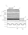
図1は、III族窒化物半導体層を有する半導体発光素子の一例を示した断面図である。図1に示すように、半導体発光素子Iは、表面に複数の凸部102が形成された基板11と、基板11の複数の凸部102が形成された面上に成膜されたバッファ層12と、複数の凸部102を埋めるようにバッファ層12上に成膜された下地層13と、下地層13上にLED構造20が形成された構造を有している。
LED構造20は、n型半導体層14、発光層15、p型半導体層16が順次積層されている。LED構造20を構成するn型半導体層14は、n型コンタクト層14a及びn型クラッド層14bを有する。発光層15は、障壁層15a及び井戸層15bが交互に積層された構造を有する。p型半導体層16は、p型クラッド層16a及びp型コンタクト層16bが積層されている。
さらに、p型半導体層16上に透明正極17が積層され、その上に正極ボンディングパッド18が形成されるとともに、n型半導体層14のn型コンタクト層14aに形成された露出領域14dに負極19が積層されている。
(Semiconductor light emitting element I)
FIG. 1 is a cross-sectional view showing an example of a semiconductor light emitting device having a group III nitride semiconductor layer. As shown in FIG. 1, the semiconductor light emitting device I includes a
In the
Further, a transparent
(基板11)
基板11は、III族窒化物化合物半導体とは異なる材料から構成される。基板11を構成する材料としては、例えば、サファイア、炭化ケイ素(シリコンカーバイド:SiC)、シリコン、酸化亜鉛、酸化マグネシウム、酸化マンガン、酸化ジルコニウム、酸化マンガン亜鉛鉄、酸化マグネシウムアルミニウム、ホウ化ジルコニウム、酸化ガリウム、酸化インジウム、酸化リチウムガリウム、酸化リチウムアルミニウム、酸化ネオジウムガリウム、酸化ランタンストロンチウムアルミニウムタンタル、酸化ストロンチウムチタン、酸化チタン、ハフニウム、タングステン、モリブデン等が挙げられる。これらの中でも、サファイア、炭化ケイ素(シリコンカーバイド:SiC)が好ましく、サファイアが特に好ましい。
(Substrate 11)
The
本実施の形態では、後述するように、基板11の被研削面103を所定の研削装置により研削し、その後、研磨装置により研磨することにより、基板11の厚さは、通常、170μm以下であり、好ましくは160μm以下となるように調整されている。但し、基板11の厚さは、通常、70μm以上である。
さらに、本実施の形態では、基板11の裏面である被研削面103の表面粗さRaが、3nm〜25nm、好ましくは、5nm〜20nmになるように調整されている。
基板11の裏面を上述した範囲の表面粗さRaを有する粗面として調整することにより、基板11の反りが低減し、基板11の平坦性を保つことができる。
また、被研削面103における光の乱反射により、半導体発光素子Iの光取り出し効率が増大する。
さらに、後述するように、基板11内部に改質領域を形成するために、基板11の被研削面103側からレーザ光を照射する際に、レーザ光の焦光点を正確に合わせることが可能となる。
In the present embodiment, as will be described later, the thickness of the
Furthermore, in the present embodiment, the surface roughness Ra of the surface to be
By adjusting the back surface of the
Further, the light extraction efficiency of the semiconductor light emitting element I increases due to the irregular reflection of light on the surface to be
Further, as will be described later, in order to form a modified region inside the
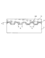
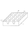
(複数の凸部102)
図2及び図3は、複数の凸部102が形成された基板11を説明する図である。図2に示すように、基板11に形成された複数の凸部102は、所定の最大径d1と高さhを有し、均一な大きさと均一な形状になるように形成されている。本実施の形態では、凸部102の形状は半球状である。尚、凸部102の形状は特に限定されない。
本実施の形態では、凸部102の最大径d1は、0.5μm〜2μmの範囲である。凸部102の高さhは、0.5μm〜2μmの範囲である。さらに、複数の凸部102は、基板11の表面に所定の間隔d2を設けて配置されている。本実施の形態では、複数の凸部102の間隔d2は、0.5μm〜2μmの範囲である。
また、図3に示すように、複数の凸部102は、基板11の表面101S上に碁盤目状に等間隔に配置されている。
本実施形態では、基板11上に均一な形状の複数の凸部102を形成することにより、基板11と下地層13との界面が凹凸形状となる。そのため、このような構造を有する基板11の上にLED構造20を設けた半導体発光素子Iは、界面における光の乱反射により、光取り出し効率がさらに増大する。
(Multiple convex portions 102)
2 and 3 are diagrams illustrating the
In the present embodiment, the maximum diameter d 1 of the
Further, as shown in FIG. 3, the plurality of
In the present embodiment, by forming a plurality of
(バッファ層12)
バッファ層12は、後述するように半導体発光素子のLED構造を有する化合物半導体層を有機金属化学気相成長法(MOCVD)により成膜する際に、バッファ機能を発揮する薄膜層として基板11上に設けられる。バッファ層12を設けることにより、バッファ層12上に成膜される下地層13とさらにこの上に成膜されるLED構造20を有する化合物半導体層は、良好な配向性及び結晶性を有する結晶膜となる。
(Buffer layer 12)
As will be described later, the
バッファ層12を構成するIII族窒化物半導体としては、Alを含有することが好ましく、III族窒化物であるAlNを含むことが特に好ましい。バッファ層12を構成する材料としては、一般式AlGaInNで表されるIII族窒化物半導体であれば特に限定されない。さらに、V族として、AsやPが含有されても良い。バッファ層12が、Alを含む組成の場合、AlGaNとすることが好ましく、Alの組成が50%以上であることが好ましい。
本実施の形態では、バッファ層12の厚さは、0.01μm〜0.5μmである。バッファ層12の厚さが過度に薄いと、バッファ層12による基板11と下地層13との格子定数の違いを緩和する効果が十分に得られない場合がある。バッファ層12の厚さが過度に厚いと、成膜処理時間が長くなり、生産性が低下する傾向がある。
The group III nitride semiconductor constituting the
In the present embodiment, the thickness of the
(下地層13)
下地層13に用いる材料としては、Gaを含むIII族窒化物(GaN系化合物半導体)が用いられ、特に、AlGaN、又はGaNを好適に用いることができる。本実施の形態における下地層13は、LED構造20を有する化合物半導体層の下地層として機能するものである。
本実施の形態では、下地層13の厚さは、0.1μm以上、好ましく0.5μm以上、さらに好ましくは1μm以上である。但し、下地層13の厚さは、通常、10.0μm以下である。
(Underlayer 13)
As the material used for the
In the present embodiment, the thickness of the
(LED構造20)
前述したように、LED構造20を構成するn型半導体層14は、n型コンタクト層14a及びn型クラッド層14bを有する。発光層15は、障壁層15a及び井戸層15bが交互に積層された構造を有する。p型半導体層16は、p型クラッド層16a及びp型コンタクト層16bが積層されている。
(LED structure 20)
As described above, the n-
(n型半導体層14)
n型半導体層14のn型コンタクト層14aとしては、下地層13と同様にGaN系化合物半導体が用いられる。また、下地層13及びn型コンタクト層14aを構成する窒化ガリウム系化合物半導体は同一組成であることが好ましく、これらの合計の膜厚を0.1μm〜20μm、好ましくは0.5μm〜15μm、さらに好ましくは1μm〜12μmの範囲に設定することが好ましい。
(N-type semiconductor layer 14)
As the n-
n型クラッド層14bは、AlGaN、GaN、GaInN等によって形成することが可能である。また、これらの構造のヘテロ接合や複数回積層した超格子構造としてもよい。GaInNとする場合には、発光層15のGaInNのバンドギャップよりも大きくすることが望ましい。n型クラッド層14bの膜厚は、好ましくは5nm〜500nm、より好ましくは5nm〜100nmの範囲である。
The n-
(発光層15)
発光層15は、窒化ガリウム系化合物半導体からなる障壁層15aと、インジウムを含有する窒化ガリウム系化合物半導体からなる井戸層15bとが交互に繰り返して積層され、且つ、n型半導体層14側及びp型半導体層16側に障壁層15aが配される順で積層して形成される。本実施の形態では、発光層15は、6層の障壁層15aと5層の井戸層15bとが交互に繰り返して積層され、発光層15の最上層及び最下層に障壁層15aが配され、各障壁層15aの間に井戸層15bが配される構成とされている。
(Light emitting layer 15)
The
障壁層15aとしては、例えば、インジウムを含有した窒化ガリウム系化合物半導体からなる井戸層15bよりもバンドギャップエネルギーが大きいAlcGa1−cN(0≦c≦0.3)等の窒化ガリウム系化合物半導体を好適に用いることができる。
また、井戸層15bには、インジウムを含有する窒化ガリウム系化合物半導体として、例えば、Ga1−sInsN(0<s<0.4)等の窒化ガリウムインジウムを用いることができる。
As the
Furthermore, the
(p型半導体層16)
p型半導体層16は、p型クラッド層16a及びp型コンタクト層16bから構成される。p型クラッド層16aとしては、好ましくは、AldGa1−dN(0<d≦0.4)のものが挙げられる。p型クラッド層16aの膜厚は、好ましくは1nm〜400nmであり、より好ましくは5nm〜100nmである。
p型コンタクト層16bとしては、少なくともAleGa1−eN(0≦e<0.5)を含んでなる窒化ガリウム系化合物半導体層が挙げられる。p型コンタクト層16bの膜厚は、特に限定されないが、10nm〜500nmが好ましく、より好ましくは50nm〜200nmである。
(P-type semiconductor layer 16)
The p-
Examples of the p-
(透明正極17)
透明正極17を構成する材料としては、例えば、ITO(In2O3−SnO2)、AZO(ZnO−Al2O3)、IZO(In2O3−ZnO)、GZO(ZnO−Ga2O3)等の従来公知の材料が挙げられる。また、透明正極17の構造は特に限定されず、従来公知の構造を採用することができる。透明正極17は、p型半導体層16上のほぼ全面を覆うように形成しても良く、格子状や樹形状に形成しても良い。
(Transparent positive electrode 17)
Examples of the material constituting the transparent
(正極ボンディングパッド18)
透明正極17上に形成される電極としての正極ボンディングパッド18は、例えば、従来公知のAu、Al、Ni、Cu等の材料から構成される。正極ボンディングパッド18の構造は特に限定されず、従来公知の構造を採用することができる。
正極ボンディングパッド18の厚さは、100nm〜1000nmの範囲内であり、好ましくは300nm〜500nmの範囲内である。
(Positive electrode bonding pad 18)
The positive
The thickness of the positive
(負極19)
図1に示すように、負極19は、基板11上に成膜されたバッファ層12及び下地層13の上にさらに成膜されたLED構造20(n型半導体層14、発光層15及びp型半導体層16)において、n型半導体層14のn型コンタクト層14aに接するように形成される。このため、負極19を形成する際は、p型半導体層16、発光層15及びn型半導体層14の一部を除去し、n型コンタクト層14aの露出領域14dを形成し、この上に負極19を形成する。
負極19の材料としては、各種組成および構造の負極が周知であり、これら周知の負極
を何ら制限無く用いることができ、この技術分野でよく知られた慣用の手段で設けること
ができる。
(Negative electrode 19)
As shown in FIG. 1, the
As the material of the
(半導体発光素子の製造方法)
次に、本実施の形態が適用される半導体発光素子の製造方法について説明する。
図4、図5、図6は、半導体発光素子の製造工程を説明する図である。
図4(a)に示すように、先ず、サファイア板10を準備する。サファイア板10の最大径は、通常、約50mm以上、好ましくは約100mm以上の範囲であり、約50mm〜約200mmの範囲がより好ましい。厚さは、0.4mm〜2mmの範囲が好ましい。
本実施の形態では、(1)最大径約50mmと厚さ0.7mmを有するサファイア板10、(2)最大径約100mmと厚さ1mmを有するサファイア板10、(3)最大径約150mmと厚さ1.3mmを有するサファイア板10を使用する。
(Manufacturing method of semiconductor light emitting device)
Next, a method for manufacturing a semiconductor light emitting element to which the present embodiment is applied will be described.
4, 5, and 6 are diagrams illustrating a manufacturing process of the semiconductor light emitting device.
As shown in FIG. 4A, first, a
In the present embodiment, (1) a
次に、図4(b)に示すように、サファイア板10の表面に均一な形状を有する複数の凸部102が形成された基板11を加工する(基板加工工程)。基板11の加工では、基板11上における凸部102の平面配置を規定するマスクを形成するパターニングと、パターニングによって形成されたマスクを使って基板11をエッチングして凸部102を形成するエッチングとを行なう。パターニングは、一般的なフォトリソグラフィー法で行なうことができる。エッチングは、ドライエッチング法を用いることが好ましい。
Next, as shown in FIG. 4B, the
尚、凸部102を形成する方法としては、上述したエッチング法に限定されない。例えば、サファイア板10に凸部102となる材料を、スパッタ法、蒸着法、CVD法等により積層させることにより凸部を形成してもよい。この場合、凸部102となる材料としては、サファイア板10とほぼ同等の屈折率を有する材料を用いることが好ましく、例えば、Al2O3、SiN、SiO2等を用いることができる。
Note that the method for forming the
続いて、図4(c)に示すように、基板11の表面101S上にIII族窒化物半導体からなるバッファ層12を形成する(バッファ層形成工程)。本実施の形態では、バッファ層12は、III族窒化物半導体をスパッタリングすることにより形成することが好ましい。スパッタリングによりバッファ層12を形成する場合、チャンバ内の窒素原料と不活性ガスの流量の比を、窒素原料が50%〜100%、望ましくは75%となるようにすることが望ましい。
Subsequently, FIG. 4 (c), the forming the
また、スパッタ法によって、柱状結晶(多結晶)を有するバッファ層12を形成する場合、チャンバ内の窒素原料と不活性ガスの流量の比を、窒素原料が1%〜50%、望ましくは25%となるようにすることが望ましい。これにより、V族元素を窒素とし、バッファ層12を成膜する際のガス中における窒素のガス分率を50%〜99%以下の範囲とするとともに、バッファ層12を単結晶組織として形成する。その結果、短時間で良好な結晶性を有するバッファ層12を、特定の異方性を持つ配向膜として基板11上に成膜することができ、さらに、バッファ層12上に、結晶性の良好なIII族窒化物半導体を効率良く成長させることが可能となる。
Further, when the
次に、図4(d)に示すように、本実施形態では、バッファ層12を形成工程の後、バッファ層12が形成された基板11の上面上に、凸部102を埋めるようにして、MOCVD法によりIII族窒化物半導体からなる下地層13を成膜する。尚、本実施の形態では、下地層13の最大厚さHは、凸部102の高さhの2倍以上であることが好ましい。
Next, as shown in FIG. 4D, in this embodiment, after the step of forming the
次に、図5(a)に示すように、成膜した下地層13上に、MOCVD法により、n型半導体層14、発光層15、及びp型半導体層16を順次積層し、半導体発光素子ウェーハI0を形成する。
Next, as shown in FIG. 5A, an n-
下地層13、及びn型半導体層14、発光層15、p型半導体層16をMOCVD法で積層する場合に使用するキャリアガスとしては、例えば、水素(H2)、窒素(N3);III族原料であるGa源としてトリメチルガリウム(TMG)、トリエチルガリウム(TEG);Al源としてトリメチルアルミニウム(TMA)、トリエチルアルミニウム(TEA);In源としてトリメチルインジウム(TMI)、トリエチルインジウム(TEI);V族原料であるN源としてアンモニア(NH3)、ヒドラジン(N2H4)等が用いられる。また、ドーパントとしては、n型にはSi原料としてモノシラン(SiH4)、ジシラン(Si2H6);Ge原料としてゲルマンガス(GeH4)、テトラメチルゲルマニウム((CH3)4Ge)、テトラエチルゲルマニウム((C2H5)4Ge)等の有機ゲルマニウム化合物;p型にはMg原料としてシクロペンタジエニルマグネシウム(Cp2Mg)を利用できる。
As the carrier gas used when the
本実施の形態において、基板11に下地層13を形成することにより、この上に成膜されるIII族窒化物半導体からなるn型半導体層14、発光層15、p型半導体層16からなるLED構造20の結晶の結晶性が良好となる。その結果、内部量子効率に優れ、リークの少ない半導体発光素子Iが得られる。
尚、LED構造20の内、下地層13をMOCVD法によって形成した後、n型コンタクト層14a及びn型クラッド層14bの各層をスパッタ法で形成し、その上の発光層15をMOCVD法で形成し、そして、p型半導体層16を構成するp型クラッド層16a及びp型コンタクト層16bの各層を反応性スパッタ法で形成してもよい。
In the present embodiment, by forming the
In the
次に、図5(b)に示すように、基板11上にバッファ層12、下地層13及びLED構造20を成膜した後、LED構造20のp型半導体層16上に透明正極17を積層し、その上に正極ボンディングパッド18を形成する。続いて、LED構造20の所定の位置をエッチング除去することにより、n型半導体層14を露出させて複数の露出領域14dを形成し、露出領域14dの各々に正極ボンディングパッド18と対になるように複数の負極19を形成する。
Next, as shown in FIG. 5B, the
負極19を形成する際は、まず、基板11上に形成されたp型半導体層16、発光層15及びn型半導体層14の一部をドライエッチング等の方法によって除去し、n型コンタクト層14aの露出領域14dを形成する。そして、この露出領域14d上に、例えば、露出領域14d表面側から順に、Ni、Al、Ti、Auの各材料を従来公知の方法で積層することにより、詳細な図示を省略する4層構造の負極19を形成することができる。
When forming the
続いて、図5(c)に示すように、基板11が所定の厚さになるまで基板11の被研削面103を、研削及び研磨する(研削工程・研磨工程)。本実施の形態では、約20分間程度の研削工程により、基板11を研削し、基板11の厚さを、例えば、約1000μmから約120μm迄減少させる。さらに、本実施の形態では、研削工程に続き、約15分間の研磨工程により、基板11の厚さを、約120μmから約80μm迄に研磨する。
ここで、本実施の形態では、研削工程及び研磨工程により、基板11の厚さを調整するとともに、基板11の裏面である被研削面103の表面粗さRaを、3nm〜25nm、好ましくは、5nm〜20nmになるように調整する。
Subsequently, as shown in FIG. 5C, the surface to be ground 103 of the
Here, in the present embodiment, the thickness of the
被研削面103の表面粗さRaを上述した範囲に調整する方法は特に限定されないが、例えば、基板11の被研削面103を研削・研磨する際に、被研削面103と所定の研削・研磨装置の研削定盤の被研削面103とが摺り合わされる部分に研削材または研磨材を供給する。研削材または研磨材の種類は特に限定されず、市販のスラリー型の研削材または研磨材を使用することができる。
A method for adjusting the surface roughness Ra of the surface to be ground 103 to the above-described range is not particularly limited. A grinding material or an abrasive is supplied to a portion of the grinding surface plate of the apparatus where the
また、本実施の形態において、表面粗さRaのその測定方法は特に限定されないが、例えば、AFM(原子間力顕微鏡;Atomic Force Microscope)、SEM(走査型電子顕微鏡;Scanning Electron Microscope)等による視野角解析による公知の方法で、算術平均粗さRaとして求めることができる。 In the present embodiment, the method for measuring the surface roughness Ra is not particularly limited. For example, the field of view by AFM (Atomic Force Microscope), SEM (Scanning Electron Microscope), or the like. It can obtain | require as arithmetic mean roughness Ra by the well-known method by an angular analysis.
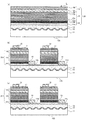
次に、図6(a)に示すように、LED構造20側からn型コンタクト層14aの露出領域14dにレーザL1を照射し割溝30を形成する(割溝形成工程)。割溝30は、後述するように、基板11を分割するための切断予定ラインに沿ってレーザL1を照射することにより形成する。割溝30の幅は特に制限されない。本実施の形態では、割溝30の深さは、通常、基板11の表面から6μm以上であり、10μm以上であることが好ましく、20μm以上であることがさらに好ましい。割溝30の深さが過度に小さいと、切断面が斜めに割れ、不良チップが生成する傾向がある。
Next, as shown in FIG. 6A, the laser groove L30 is formed by irradiating the exposed
割溝30の断面形状は矩形、U字状、V字状等の形状が採用され、好ましくは、V字状またはU字状であり、V字状が特に好ましい。割溝30の断面形状がV字状の場合、チップ状に分割する際、V字状の最先端付近からクラックが発生し、不良率が低下する傾向がある。尚、割溝30の断面形状は、ビーム径および焦点位置等のレーザ光学系の制御によりコントロール可能である。
The sectional shape of the dividing
続いて、図6(b)に示すように、前述した研磨工程により表面粗さRaを調整した基板11の被研削面103側から、基板11を分割するための切断予定ラインに沿ってレーザL2を照射することにより基板11の内部に加工変質部分(内部クラック)41,42を設ける(レーザ加工工程)。本実施の形態では、レーザ加工工程において、基板11の内部の被研削面側から厚さ方向で(2/3)部の範囲に、断続的に2個の加工変質部分41,42を設けている。
また、加工変質部分41,42は、基板11に設けた割溝30と基板11の厚さ方向に略同一の直線上に形成している。
Subsequently, as shown in FIG. 6B, the laser L2 along the planned cutting line for dividing the
Further, the work-affected
本実施の形態において加工変質部分41,42とは、例えば、サファイア製の基板11の内部にレーザL2の焦光点を合わせて照射することにより、基板11のレーザL2が照射された部分が溶融・再固化した改質領域や多光子吸収による改質領域等を言う。この場合、レーザ照射による溶融・再固化に伴い生じる微小なクラックの発生も含まれる。
In the present embodiment, the work-affected
具体的には、例えば、ステルスレーザ加工機(図示せず)を用い、エキシマ励起のパルスレーザを照射しながら、基板11を分割するための切断予定ラインに沿ってレーザL2を照射する。この際、基板11上に照射するレーザL2の焦点を変化させることにより、基板11の厚さ方向において複数箇所(図6(b)では2箇所)に設けることが可能となる。
Specifically, for example, using a stealth laser processing machine (not shown), the laser L2 is irradiated along the planned cutting line for dividing the
使用するレーザとしては、例えば、CO2レーザ、YAG(イットリウム・アルミニウム・ガーネット)レーザ等が挙げられる。本実施の形態では、パルス照射のレーザを用いることが最も好ましい。本実施の形態では、レーザL2の波長としては、266nm又は355nmを使用している。また、基板11の切断予定ラインに沿ってレーザL2を間欠的に照射(パルス照射)することにより、基板11の内部に効果的にダメージを付与し、この部分を揮散あるいは強度的に弱い材質へと変換させることができる。この場合、パルス周期を、10〜40Hzの範囲とすることが好ましい。
Examples of the laser to be used include a CO2 laser and a YAG (yttrium / aluminum / garnet) laser. In this embodiment mode, it is most preferable to use a pulsed laser. In the present embodiment, 266 nm or 355 nm is used as the wavelength of the laser L2. Further, by intermittently irradiating the laser L2 along the planned cutting line of the substrate 11 (pulse irradiation), the inside of the
次に、図6(c)に示すように、基板11を加工変質部分41,42に沿って切断し、複数のチップに分割する(分割工程)。具体的には、例えば、ブレーカ装置(図示せず)を用い、割溝30及び加工変質部分41,42に沿うようにブレード(図示せず)を押し当てることにより、加工変質部分41,42に沿って基板11を押し割り、複数のチップに分割する。
Next, as shown in FIG. 6C, the
本実施形態では、分割工程において、割溝30及び加工変質部分41,42に沿って基板11を個々の発光素子単位のチップに切断することで、加工変質部分41,42を起点として、基板11に亀裂を生じさせつつ、半導体発光素子ウェーハI0(図5(a)参照)を個々のチップ状態の半導体発光素子Iに分割することができる。
このとき、分割後の基板11の分割面(端面11a)には、加工変質部分41,42の少なくとも一部が残存する領域と、基板11を切断した際に分割面(端面11a)に生じる亀裂痕が不規則に残存する領域とが存在し、分割面(端面11a)のほぼ全体が粗面となる。
このように、基板11の分割面(端面11a)を粗面として形成することにより、分割面(端面11a)の表面積が増加し、入射した光を効率良く外部に出射できる基板11とすることができ、光取り出し効率に優れた半導体発光素子Iを製造することが可能となる。
In the present embodiment, in the dividing step, the
At this time, on the divided surface (end
Thus, by forming the dividing surface (end
本実施の形態においてIII族窒化物半導体発光素子は、通常、基板11上にLED構造20を成膜し、次いで、基板11の被研削面103を研削・研磨処理によって所定の厚さに調整し、その後、適当な大きさに切断し、所定の厚さの基板11を有する半導体発光素子チップとして得られる。
In the present embodiment, the group III nitride semiconductor light-emitting device usually has the
本実施の形態においては、半導体層と基板の熱膨張係数の違いに起因して、基板の薄板化後のウェーハの反りにも影響してくる。特に、発光層を含む半導体層の膜厚が5μm以上の場合には半導体層膜厚が厚くなるほど反りが大きくなり、その後のレーザ加工工程に悪い影響を及ぼす。
しかしながら、本実施の形態が適用される半導体発光素子の製造方法によれば、研磨工程において、研削工程で研削された基板の被研削面の表面粗さRaを3nm〜25nmに調整することにより、レーザ加工工程における基板の平坦性を保つことができる。
このような効果は、基板、例えば、サファイア基板の最大径が、大きいものほど格別となる。本実施の形態では、最大径が、約50mm<約100mm<約150mmの順で、特に効果的であった。
In this embodiment, due to the difference in the thermal expansion coefficient between the semiconductor layer and the substrate, the warpage of the wafer after the substrate is thinned is also affected. In particular, when the thickness of the semiconductor layer including the light emitting layer is 5 μm or more, the warpage increases as the semiconductor layer thickness increases, which adversely affects the subsequent laser processing steps.
However, according to the method for manufacturing a semiconductor light emitting element to which the present embodiment is applied, in the polishing process, by adjusting the surface roughness Ra of the ground surface of the substrate ground in the grinding process to 3 nm to 25 nm, The flatness of the substrate in the laser processing step can be maintained.
Such an effect becomes more significant as the maximum diameter of the substrate, for example, the sapphire substrate is larger. In the present embodiment, the maximum diameter is particularly effective in the order of about 50 mm <about 100 mm <about 150 mm.
上述したように、本実施の形態が適用される半導体発光素子Iは、例えば、これと蛍光体とを組み合わせてなるランプとして使用することができる。半導体発光素子Iと蛍光体とを組み合わせたランプは、当業者周知の手段によって当業者周知の構成とすることができる。また、従来より、III族窒化物半導体発光素子と蛍光体と組み合わせることによって発光色を変える技術を採用することが可能である。ランプの例としては、一般用途の砲弾型、携帯のバックライト用途のサイドビュー型、表示器に用いられるトップビュー型等いかなる用途にも用いることができる。 As described above, the semiconductor light emitting element I to which the present embodiment is applied can be used as, for example, a lamp formed by combining this and a phosphor. A lamp in which the semiconductor light emitting element I and the phosphor are combined can have a configuration well known to those skilled in the art by means well known to those skilled in the art. Conventionally, it is possible to employ a technique for changing the emission color by combining a group III nitride semiconductor light emitting device and a phosphor. As an example of the lamp, it can be used for any purpose such as a bullet type for general use, a side view type for portable backlight use, and a top view type used for a display.
10…サファイア板、11…基板、11a…分割面(端面)、12…バッファ層、13…下地層、14…n型半導体層、15…発光層、16…p型半導体層、17…透明正極、18…正極ボンディングパッド、19…負極、20…LED構造、30…割溝、41,42…加工変質部分(内部クラック)、102…凸部、103…被研削面、I…半導体発光素子
DESCRIPTION OF
Claims (11)
基板と当該基板上に成膜されたIII族窒化物半導体の積層構造からなるIII族窒化物半導体層とを有するウェーハの当該基板の被研削面を研削する研削工程と、
前記研削工程により研削された前記基板の前記被研削面の表面粗さRaを3nm〜25nmに調整する研磨工程と、
前記研磨工程により前記表面粗さRaを調整した前記基板の前記被研削面側から、当該基板を分割するための切断予定ラインに沿ってレーザを照射することにより、当該基板の内部に加工変質部分を設けるレーザ加工工程と、
前記レーザ加工工程により前記加工変質部分を設けた前記基板を当該加工変質部分及び前記切断予定ラインに沿って分割する分割工程と、
を有することを特徴とする半導体発光素子の製造方法。 A method of manufacturing a semiconductor light emitting device having a group III nitride semiconductor layer,
A grinding step of grinding a surface to be ground of the substrate having a substrate and a group III nitride semiconductor layer having a laminated structure of a group III nitride semiconductor formed on the substrate;
A polishing step of adjusting the surface roughness Ra of the surface to be ground of the substrate ground by the grinding step to 3 nm to 25 nm;
By applying a laser along a planned cutting line for dividing the substrate from the ground surface side of the substrate, the surface roughness Ra of which has been adjusted by the polishing step, a work-affected portion is formed inside the substrate. A laser processing step of providing
A dividing step of dividing the substrate provided with the processing-affected portion by the laser processing step along the processing-affected portion and the scheduled cutting line;
A method for manufacturing a semiconductor light emitting device, comprising:
Priority Applications (4)
| Application Number | Priority Date | Filing Date | Title |
|---|---|---|---|
| JP2008275683A JP2010103424A (en) | 2008-10-27 | 2008-10-27 | Method of manufacturing semiconductor light-emitting element |
| PCT/JP2009/068250 WO2010050410A1 (en) | 2008-10-27 | 2009-10-23 | Method for manufacturing semiconductor light emitting element |
| US13/126,136 US20110204412A1 (en) | 2008-10-27 | 2009-10-23 | Method for manufacturing semiconductor light emitting element |
| TW098136325A TWI427827B (en) | 2008-10-27 | 2009-10-27 | Manufacturing method of semiconductor light emitting element |
Applications Claiming Priority (1)
| Application Number | Priority Date | Filing Date | Title |
|---|---|---|---|
| JP2008275683A JP2010103424A (en) | 2008-10-27 | 2008-10-27 | Method of manufacturing semiconductor light-emitting element |
Publications (1)
| Publication Number | Publication Date |
|---|---|
| JP2010103424A true JP2010103424A (en) | 2010-05-06 |
Family
ID=42128773
Family Applications (1)
| Application Number | Title | Priority Date | Filing Date |
|---|---|---|---|
| JP2008275683A Pending JP2010103424A (en) | 2008-10-27 | 2008-10-27 | Method of manufacturing semiconductor light-emitting element |
Country Status (4)
| Country | Link |
|---|---|
| US (1) | US20110204412A1 (en) |
| JP (1) | JP2010103424A (en) |
| TW (1) | TWI427827B (en) |
| WO (1) | WO2010050410A1 (en) |
Cited By (8)
| Publication number | Priority date | Publication date | Assignee | Title |
|---|---|---|---|---|
| JP2011176379A (en) * | 2009-09-07 | 2011-09-08 | El-Seed Corp | Semiconductor light emitting device |
| WO2012023954A1 (en) * | 2010-08-20 | 2012-02-23 | Invenlux Corporation | Light-emitting devices with substrate coated with optically denser material |
| JP2012227187A (en) * | 2011-04-15 | 2012-11-15 | Showa Denko Kk | Semiconductor light-emitting chip manufacturing method and semiconductor light-emitting chip |
| JP2013098298A (en) * | 2011-10-31 | 2013-05-20 | Toyoda Gosei Co Ltd | Group iii nitride semiconductor light-emitting element manufacturing method |
| JP2013168680A (en) * | 2013-05-28 | 2013-08-29 | Toshiba Corp | Semiconductor light-emitting element and method of manufacturing the same |
| US9147599B2 (en) | 2011-10-18 | 2015-09-29 | Fuji Electric Co., Ltd. | Wafer support system and method for separating support substrate from solid-phase bonded wafer and method for manufacturing semiconductor device |
| JP2016184718A (en) * | 2015-03-24 | 2016-10-20 | 日亜化学工業株式会社 | Manufacturing method for light emission element |
| US9873170B2 (en) | 2015-03-24 | 2018-01-23 | Nichia Corporation | Method of manufacturing light emitting element |
Families Citing this family (18)
| Publication number | Priority date | Publication date | Assignee | Title |
|---|---|---|---|---|
| JP5222916B2 (en) * | 2010-09-17 | 2013-06-26 | シャープ株式会社 | Semiconductor substrate manufacturing method, semiconductor device, and electrical apparatus |
| US8722516B2 (en) * | 2010-09-28 | 2014-05-13 | Hamamatsu Photonics K.K. | Laser processing method and method for manufacturing light-emitting device |
| DE102011012925A1 (en) * | 2011-03-03 | 2012-09-06 | Osram Opto Semiconductors Gmbh | Method for producing an optoelectronic semiconductor chip |
| TWI430475B (en) * | 2011-08-03 | 2014-03-11 | Lextar Electronics Corp | Method of manufacturing light emitting diode |
| CN102290505B (en) * | 2011-09-09 | 2014-04-30 | 上海蓝光科技有限公司 | GaN-base light-emitting diode chip and manufacturing method thereof |
| US20140361329A1 (en) * | 2012-02-02 | 2014-12-11 | Koninklijke Philips N.V. | Producing light emitting devices at variable flux levels |
| US20130234149A1 (en) * | 2012-03-09 | 2013-09-12 | Electro Scientific Industries, Inc. | Sidewall texturing of light emitting diode structures |
| KR101233062B1 (en) * | 2012-04-18 | 2013-02-19 | (주)휴넷플러스 | Method for fabricating nano patterned substrate for high efficiency nitride based light emitting diode |
| US9040389B2 (en) | 2012-10-09 | 2015-05-26 | Infineon Technologies Ag | Singulation processes |
| CN103022284A (en) * | 2013-01-08 | 2013-04-03 | 聚灿光电科技(苏州)有限公司 | LED chip cutting method and LED chip manufactured by same |
| US9548419B2 (en) * | 2014-05-20 | 2017-01-17 | Southern Taiwan University Of Science And Technology | Light emitting diode chip having multi microstructure substrate surface |
| TWI614914B (en) * | 2014-07-11 | 2018-02-11 | 晶元光電股份有限公司 | Light-emitting element and method of manufacturing same |
| CN111430511A (en) * | 2014-07-25 | 2020-07-17 | 晶元光电股份有限公司 | Light-emitting element and method of manufacturing the same |
| WO2016202039A1 (en) * | 2015-06-17 | 2016-12-22 | 厦门市三安光电科技有限公司 | Light emitting diode and preparation method thereof |
| US10505072B2 (en) * | 2016-12-16 | 2019-12-10 | Nichia Corporation | Method for manufacturing light emitting element |
| TWI846791B (en) * | 2019-12-31 | 2024-07-01 | 晶元光電股份有限公司 | Light-emitting element and manufacturing method thereof |
| CN113228310A (en) * | 2020-12-30 | 2021-08-06 | 泉州三安半导体科技有限公司 | Semiconductor light-emitting element and preparation method thereof |
| JP7534656B2 (en) | 2022-03-15 | 2024-08-15 | 日亜化学工業株式会社 | Light-emitting device manufacturing method and light-emitting device |
Citations (10)
| Publication number | Priority date | Publication date | Assignee | Title |
|---|---|---|---|---|
| JP2002053398A (en) * | 2000-08-03 | 2002-02-19 | Hitachi Cable Ltd | Crystal substrate |
| JP2003218065A (en) * | 2002-11-13 | 2003-07-31 | Nichia Chem Ind Ltd | Method for manufacturing nitride semiconductor device |
| JP2003318441A (en) * | 2001-07-24 | 2003-11-07 | Nichia Chem Ind Ltd | Semiconductor light emitting device |
| JP2005244198A (en) * | 2004-01-26 | 2005-09-08 | Matsushita Electric Ind Co Ltd | Manufacturing method of semiconductor device |
| JP2006024914A (en) * | 2004-06-11 | 2006-01-26 | Showa Denko Kk | Method for manufacturing compound semiconductor device wafer |
| JP2006169104A (en) * | 2000-09-18 | 2006-06-29 | Mitsubishi Cable Ind Ltd | Semiconductor base-material and its manufacturing method |
| JP2006245380A (en) * | 2005-03-04 | 2006-09-14 | Toshiba Corp | Semiconductor light emitting device and method for manufacturing semiconductor light emitting device |
| JP2008106316A (en) * | 2006-10-26 | 2008-05-08 | Showa Denko Kk | Method for producing group III nitride compound semiconductor light emitting device, group III nitride compound semiconductor light emitting device, and lamp |
| JP2008117799A (en) * | 2006-10-31 | 2008-05-22 | Stanley Electric Co Ltd | Semiconductor substrate processing method, semiconductor device manufacturing method, and ZnO substrate |
| JP2008251753A (en) * | 2007-03-29 | 2008-10-16 | Mitsubishi Chemicals Corp | Manufacturing method of nitride LED element |
Family Cites Families (10)
| Publication number | Priority date | Publication date | Assignee | Title |
|---|---|---|---|---|
| US6903385B2 (en) * | 2002-10-09 | 2005-06-07 | Sensor Electronic Technology, Inc. | Semiconductor structure having a textured nitride-based layer |
| US7008861B2 (en) * | 2003-12-11 | 2006-03-07 | Cree, Inc. | Semiconductor substrate assemblies and methods for preparing and dicing the same |
| JP2005268752A (en) * | 2004-02-19 | 2005-09-29 | Canon Inc | Laser cleaving method, member to be cleaved, and semiconductor element chip |
| US7772605B2 (en) * | 2004-03-19 | 2010-08-10 | Showa Denko K.K. | Compound semiconductor light-emitting device |
| US7875898B2 (en) * | 2005-01-24 | 2011-01-25 | Panasonic Corporation | Semiconductor device |
| US7829909B2 (en) * | 2005-11-15 | 2010-11-09 | Verticle, Inc. | Light emitting diodes and fabrication methods thereof |
| US7838331B2 (en) * | 2005-11-16 | 2010-11-23 | Denso Corporation | Method for dicing semiconductor substrate |
| JP4908381B2 (en) * | 2006-12-22 | 2012-04-04 | 昭和電工株式会社 | Group III nitride semiconductor layer manufacturing method, group III nitride semiconductor light emitting device, and lamp |
| WO2008083081A2 (en) * | 2006-12-28 | 2008-07-10 | Saint-Gobain Ceramics & Plastics, Inc. | Sapphire substrates and methods of making same |
| US8236591B2 (en) * | 2007-08-03 | 2012-08-07 | Nichia Corporation | Semiconductor light emitting element and method for manufacturing the same |
-
2008
- 2008-10-27 JP JP2008275683A patent/JP2010103424A/en active Pending
-
2009
- 2009-10-23 WO PCT/JP2009/068250 patent/WO2010050410A1/en not_active Ceased
- 2009-10-23 US US13/126,136 patent/US20110204412A1/en not_active Abandoned
- 2009-10-27 TW TW098136325A patent/TWI427827B/en active
Patent Citations (10)
| Publication number | Priority date | Publication date | Assignee | Title |
|---|---|---|---|---|
| JP2002053398A (en) * | 2000-08-03 | 2002-02-19 | Hitachi Cable Ltd | Crystal substrate |
| JP2006169104A (en) * | 2000-09-18 | 2006-06-29 | Mitsubishi Cable Ind Ltd | Semiconductor base-material and its manufacturing method |
| JP2003318441A (en) * | 2001-07-24 | 2003-11-07 | Nichia Chem Ind Ltd | Semiconductor light emitting device |
| JP2003218065A (en) * | 2002-11-13 | 2003-07-31 | Nichia Chem Ind Ltd | Method for manufacturing nitride semiconductor device |
| JP2005244198A (en) * | 2004-01-26 | 2005-09-08 | Matsushita Electric Ind Co Ltd | Manufacturing method of semiconductor device |
| JP2006024914A (en) * | 2004-06-11 | 2006-01-26 | Showa Denko Kk | Method for manufacturing compound semiconductor device wafer |
| JP2006245380A (en) * | 2005-03-04 | 2006-09-14 | Toshiba Corp | Semiconductor light emitting device and method for manufacturing semiconductor light emitting device |
| JP2008106316A (en) * | 2006-10-26 | 2008-05-08 | Showa Denko Kk | Method for producing group III nitride compound semiconductor light emitting device, group III nitride compound semiconductor light emitting device, and lamp |
| JP2008117799A (en) * | 2006-10-31 | 2008-05-22 | Stanley Electric Co Ltd | Semiconductor substrate processing method, semiconductor device manufacturing method, and ZnO substrate |
| JP2008251753A (en) * | 2007-03-29 | 2008-10-16 | Mitsubishi Chemicals Corp | Manufacturing method of nitride LED element |
Cited By (10)
| Publication number | Priority date | Publication date | Assignee | Title |
|---|---|---|---|---|
| JP2011176379A (en) * | 2009-09-07 | 2011-09-08 | El-Seed Corp | Semiconductor light emitting device |
| JPWO2011027679A1 (en) * | 2009-09-07 | 2013-02-04 | エルシード株式会社 | Semiconductor light emitting device |
| WO2012023954A1 (en) * | 2010-08-20 | 2012-02-23 | Invenlux Corporation | Light-emitting devices with substrate coated with optically denser material |
| US8723201B2 (en) | 2010-08-20 | 2014-05-13 | Invenlux Corporation | Light-emitting devices with substrate coated with optically denser material |
| JP2012227187A (en) * | 2011-04-15 | 2012-11-15 | Showa Denko Kk | Semiconductor light-emitting chip manufacturing method and semiconductor light-emitting chip |
| US9147599B2 (en) | 2011-10-18 | 2015-09-29 | Fuji Electric Co., Ltd. | Wafer support system and method for separating support substrate from solid-phase bonded wafer and method for manufacturing semiconductor device |
| JP2013098298A (en) * | 2011-10-31 | 2013-05-20 | Toyoda Gosei Co Ltd | Group iii nitride semiconductor light-emitting element manufacturing method |
| JP2013168680A (en) * | 2013-05-28 | 2013-08-29 | Toshiba Corp | Semiconductor light-emitting element and method of manufacturing the same |
| JP2016184718A (en) * | 2015-03-24 | 2016-10-20 | 日亜化学工業株式会社 | Manufacturing method for light emission element |
| US9873170B2 (en) | 2015-03-24 | 2018-01-23 | Nichia Corporation | Method of manufacturing light emitting element |
Also Published As
| Publication number | Publication date |
|---|---|
| WO2010050410A1 (en) | 2010-05-06 |
| TW201025681A (en) | 2010-07-01 |
| US20110204412A1 (en) | 2011-08-25 |
| TWI427827B (en) | 2014-02-21 |
Similar Documents
| Publication | Publication Date | Title |
|---|---|---|
| JP2010103424A (en) | Method of manufacturing semiconductor light-emitting element | |
| JP5556657B2 (en) | Group III nitride semiconductor light emitting device manufacturing method, group III nitride semiconductor light emitting device, and lamp | |
| JP5179068B2 (en) | Method for manufacturing compound semiconductor device | |
| CN101467272B (en) | GaN-based compound semiconductor light-emitting element | |
| JP3904585B2 (en) | Manufacturing method of semiconductor device | |
| JP5281545B2 (en) | Manufacturing method of semiconductor light emitting device | |
| KR101454821B1 (en) | Crystalline film, device, and production methods for crystalline film and device | |
| TW200524180A (en) | Light-emitting semiconductor device, manufacturing method thereof, and electrode forming method | |
| TW201236071A (en) | Semiconductor light emitting chip and substrate processing method | |
| JP2011129765A (en) | Manufacturing method for semiconductor light-emitting element | |
| JP2005166728A (en) | Nitride semiconductor device manufacturing method | |
| US20100102341A1 (en) | Semiconductor light emitting device and method for manufacturing the same | |
| JP2007214500A (en) | Semiconductor member and manufacturing method thereof | |
| TWI327340B (en) | Production method for semiconductor device | |
| JP2008124254A (en) | Gallium nitride compound semiconductor light emitting device | |
| JP4540514B2 (en) | Compound semiconductor light emitting device and manufacturing method thereof | |
| US8866186B2 (en) | Group III nitride semiconductor light-emitting device | |
| JP2004228290A (en) | Semiconductor light emitting device and manufacturing method thereof | |
| JP2013098298A (en) | Group iii nitride semiconductor light-emitting element manufacturing method | |
| JP2005302804A (en) | Light emitting diode and manufacturing method thereof | |
| US20100038656A1 (en) | Nitride LEDs based on thick templates | |
| JP2005252245A (en) | Gallium nitride-based compound semiconductor wafer | |
| JP2006203251A (en) | Production method for semiconductor device | |
| JP4282743B2 (en) | Gallium nitride compound semiconductor light emitting device | |
| JP2008306225A (en) | Gallium nitride based compound semiconductor light-emitting device |
Legal Events
| Date | Code | Title | Description |
|---|---|---|---|
| A621 | Written request for application examination |
Free format text: JAPANESE INTERMEDIATE CODE: A621 Effective date: 20110701 |
|
| A131 | Notification of reasons for refusal |
Free format text: JAPANESE INTERMEDIATE CODE: A131 Effective date: 20121211 |
|
| A711 | Notification of change in applicant |
Free format text: JAPANESE INTERMEDIATE CODE: A711 Effective date: 20121212 |
|
| A521 | Request for written amendment filed |
Free format text: JAPANESE INTERMEDIATE CODE: A523 Effective date: 20130208 |
|
| A131 | Notification of reasons for refusal |
Free format text: JAPANESE INTERMEDIATE CODE: A131 Effective date: 20130827 |
|
| A521 | Request for written amendment filed |
Free format text: JAPANESE INTERMEDIATE CODE: A523 Effective date: 20131023 |
|
| A02 | Decision of refusal |
Free format text: JAPANESE INTERMEDIATE CODE: A02 Effective date: 20140107 |