EP3288070A1 - Semiconductor structure and fabrication method thereof - Google Patents
Semiconductor structure and fabrication method thereof Download PDFInfo
- Publication number
- EP3288070A1 EP3288070A1 EP17186344.2A EP17186344A EP3288070A1 EP 3288070 A1 EP3288070 A1 EP 3288070A1 EP 17186344 A EP17186344 A EP 17186344A EP 3288070 A1 EP3288070 A1 EP 3288070A1
- Authority
- EP
- European Patent Office
- Prior art keywords
- fins
- isolation
- layer
- region
- forming
- Prior art date
- Legal status (The legal status is an assumption and is not a legal conclusion. Google has not performed a legal analysis and makes no representation as to the accuracy of the status listed.)
- Granted
Links
- 239000004065 semiconductor Substances 0.000 title claims abstract description 103
- 238000000034 method Methods 0.000 title claims abstract description 99
- 238000004519 manufacturing process Methods 0.000 title abstract description 17
- 238000002955 isolation Methods 0.000 claims abstract description 272
- 239000000758 substrate Substances 0.000 claims abstract description 71
- 238000005530 etching Methods 0.000 claims description 27
- OKTJSMMVPCPJKN-UHFFFAOYSA-N Carbon Chemical compound [C] OKTJSMMVPCPJKN-UHFFFAOYSA-N 0.000 claims description 17
- 229910052799 carbon Inorganic materials 0.000 claims description 17
- 238000004380 ashing Methods 0.000 claims description 8
- 229920000642 polymer Polymers 0.000 claims description 5
- 125000004432 carbon atom Chemical group C* 0.000 claims description 3
- 238000005229 chemical vapour deposition Methods 0.000 claims description 3
- 230000009969 flowable effect Effects 0.000 claims description 3
- 230000003667 anti-reflective effect Effects 0.000 description 12
- 239000000463 material Substances 0.000 description 9
- 238000000059 patterning Methods 0.000 description 7
- XUIMIQQOPSSXEZ-UHFFFAOYSA-N Silicon Chemical compound [Si] XUIMIQQOPSSXEZ-UHFFFAOYSA-N 0.000 description 6
- 238000001312 dry etching Methods 0.000 description 6
- 229910052710 silicon Inorganic materials 0.000 description 6
- 239000010703 silicon Substances 0.000 description 6
- 238000005137 deposition process Methods 0.000 description 4
- 229910052732 germanium Inorganic materials 0.000 description 3
- GNPVGFCGXDBREM-UHFFFAOYSA-N germanium atom Chemical compound [Ge] GNPVGFCGXDBREM-UHFFFAOYSA-N 0.000 description 3
- VYPSYNLAJGMNEJ-UHFFFAOYSA-N silicon dioxide Inorganic materials O=[Si]=O VYPSYNLAJGMNEJ-UHFFFAOYSA-N 0.000 description 3
- 229910000577 Silicon-germanium Inorganic materials 0.000 description 2
- LEVVHYCKPQWKOP-UHFFFAOYSA-N [Si].[Ge] Chemical compound [Si].[Ge] LEVVHYCKPQWKOP-UHFFFAOYSA-N 0.000 description 2
- 230000000694 effects Effects 0.000 description 2
- 239000012212 insulator Substances 0.000 description 2
- 229910052814 silicon oxide Inorganic materials 0.000 description 2
- 238000001039 wet etching Methods 0.000 description 2
- 229910052581 Si3N4 Inorganic materials 0.000 description 1
- 125000000217 alkyl group Chemical group 0.000 description 1
- 238000009792 diffusion process Methods 0.000 description 1
- 238000005516 engineering process Methods 0.000 description 1
- 230000005669 field effect Effects 0.000 description 1
- 239000007789 gas Substances 0.000 description 1
- 230000010354 integration Effects 0.000 description 1
- 239000011368 organic material Substances 0.000 description 1
- 125000001997 phenyl group Chemical group [H]C1=C([H])C([H])=C(*)C([H])=C1[H] 0.000 description 1
- 229920002120 photoresistant polymer Polymers 0.000 description 1
- 238000007517 polishing process Methods 0.000 description 1
- HQVNEWCFYHHQES-UHFFFAOYSA-N silicon nitride Chemical compound N12[Si]34N5[Si]62N3[Si]51N64 HQVNEWCFYHHQES-UHFFFAOYSA-N 0.000 description 1
- 238000004528 spin coating Methods 0.000 description 1
- 239000000126 substance Substances 0.000 description 1
Images


Classifications
-
- H—ELECTRICITY
- H01—ELECTRIC ELEMENTS
- H01L—SEMICONDUCTOR DEVICES NOT COVERED BY CLASS H10
- H01L21/00—Processes or apparatus adapted for the manufacture or treatment of semiconductor or solid state devices or of parts thereof
- H01L21/70—Manufacture or treatment of devices consisting of a plurality of solid state components formed in or on a common substrate or of parts thereof; Manufacture of integrated circuit devices or of parts thereof
- H01L21/77—Manufacture or treatment of devices consisting of a plurality of solid state components or integrated circuits formed in, or on, a common substrate
- H01L21/78—Manufacture or treatment of devices consisting of a plurality of solid state components or integrated circuits formed in, or on, a common substrate with subsequent division of the substrate into plural individual devices
- H01L21/82—Manufacture or treatment of devices consisting of a plurality of solid state components or integrated circuits formed in, or on, a common substrate with subsequent division of the substrate into plural individual devices to produce devices, e.g. integrated circuits, each consisting of a plurality of components
- H01L21/822—Manufacture or treatment of devices consisting of a plurality of solid state components or integrated circuits formed in, or on, a common substrate with subsequent division of the substrate into plural individual devices to produce devices, e.g. integrated circuits, each consisting of a plurality of components the substrate being a semiconductor, using silicon technology
- H01L21/8232—Field-effect technology
- H01L21/8234—MIS technology, i.e. integration processes of field effect transistors of the conductor-insulator-semiconductor type
- H01L21/823481—MIS technology, i.e. integration processes of field effect transistors of the conductor-insulator-semiconductor type isolation region manufacturing related aspects, e.g. to avoid interaction of isolation region with adjacent structure
-
- H—ELECTRICITY
- H01—ELECTRIC ELEMENTS
- H01L—SEMICONDUCTOR DEVICES NOT COVERED BY CLASS H10
- H01L27/00—Devices consisting of a plurality of semiconductor or other solid-state components formed in or on a common substrate
- H01L27/02—Devices consisting of a plurality of semiconductor or other solid-state components formed in or on a common substrate including semiconductor components specially adapted for rectifying, oscillating, amplifying or switching and having potential barriers; including integrated passive circuit elements having potential barriers
- H01L27/04—Devices consisting of a plurality of semiconductor or other solid-state components formed in or on a common substrate including semiconductor components specially adapted for rectifying, oscillating, amplifying or switching and having potential barriers; including integrated passive circuit elements having potential barriers the substrate being a semiconductor body
- H01L27/08—Devices consisting of a plurality of semiconductor or other solid-state components formed in or on a common substrate including semiconductor components specially adapted for rectifying, oscillating, amplifying or switching and having potential barriers; including integrated passive circuit elements having potential barriers the substrate being a semiconductor body including only semiconductor components of a single kind
- H01L27/085—Devices consisting of a plurality of semiconductor or other solid-state components formed in or on a common substrate including semiconductor components specially adapted for rectifying, oscillating, amplifying or switching and having potential barriers; including integrated passive circuit elements having potential barriers the substrate being a semiconductor body including only semiconductor components of a single kind including field-effect components only
- H01L27/088—Devices consisting of a plurality of semiconductor or other solid-state components formed in or on a common substrate including semiconductor components specially adapted for rectifying, oscillating, amplifying or switching and having potential barriers; including integrated passive circuit elements having potential barriers the substrate being a semiconductor body including only semiconductor components of a single kind including field-effect components only the components being field-effect transistors with insulated gate
- H01L27/0886—Devices consisting of a plurality of semiconductor or other solid-state components formed in or on a common substrate including semiconductor components specially adapted for rectifying, oscillating, amplifying or switching and having potential barriers; including integrated passive circuit elements having potential barriers the substrate being a semiconductor body including only semiconductor components of a single kind including field-effect components only the components being field-effect transistors with insulated gate including transistors with a horizontal current flow in a vertical sidewall of a semiconductor body, e.g. FinFET, MuGFET
-
- H—ELECTRICITY
- H01—ELECTRIC ELEMENTS
- H01L—SEMICONDUCTOR DEVICES NOT COVERED BY CLASS H10
- H01L21/00—Processes or apparatus adapted for the manufacture or treatment of semiconductor or solid state devices or of parts thereof
- H01L21/70—Manufacture or treatment of devices consisting of a plurality of solid state components formed in or on a common substrate or of parts thereof; Manufacture of integrated circuit devices or of parts thereof
- H01L21/71—Manufacture of specific parts of devices defined in group H01L21/70
- H01L21/76—Making of isolation regions between components
- H01L21/762—Dielectric regions, e.g. EPIC dielectric isolation, LOCOS; Trench refilling techniques, SOI technology, use of channel stoppers
- H01L21/76224—Dielectric regions, e.g. EPIC dielectric isolation, LOCOS; Trench refilling techniques, SOI technology, use of channel stoppers using trench refilling with dielectric materials
-
- H—ELECTRICITY
- H01—ELECTRIC ELEMENTS
- H01L—SEMICONDUCTOR DEVICES NOT COVERED BY CLASS H10
- H01L21/00—Processes or apparatus adapted for the manufacture or treatment of semiconductor or solid state devices or of parts thereof
- H01L21/70—Manufacture or treatment of devices consisting of a plurality of solid state components formed in or on a common substrate or of parts thereof; Manufacture of integrated circuit devices or of parts thereof
- H01L21/77—Manufacture or treatment of devices consisting of a plurality of solid state components or integrated circuits formed in, or on, a common substrate
- H01L21/78—Manufacture or treatment of devices consisting of a plurality of solid state components or integrated circuits formed in, or on, a common substrate with subsequent division of the substrate into plural individual devices
- H01L21/82—Manufacture or treatment of devices consisting of a plurality of solid state components or integrated circuits formed in, or on, a common substrate with subsequent division of the substrate into plural individual devices to produce devices, e.g. integrated circuits, each consisting of a plurality of components
- H01L21/822—Manufacture or treatment of devices consisting of a plurality of solid state components or integrated circuits formed in, or on, a common substrate with subsequent division of the substrate into plural individual devices to produce devices, e.g. integrated circuits, each consisting of a plurality of components the substrate being a semiconductor, using silicon technology
- H01L21/8232—Field-effect technology
- H01L21/8234—MIS technology, i.e. integration processes of field effect transistors of the conductor-insulator-semiconductor type
- H01L21/823418—MIS technology, i.e. integration processes of field effect transistors of the conductor-insulator-semiconductor type with a particular manufacturing method of the source or drain structures, e.g. specific source or drain implants or silicided source or drain structures or raised source or drain structures
-
- H—ELECTRICITY
- H01—ELECTRIC ELEMENTS
- H01L—SEMICONDUCTOR DEVICES NOT COVERED BY CLASS H10
- H01L21/00—Processes or apparatus adapted for the manufacture or treatment of semiconductor or solid state devices or of parts thereof
- H01L21/70—Manufacture or treatment of devices consisting of a plurality of solid state components formed in or on a common substrate or of parts thereof; Manufacture of integrated circuit devices or of parts thereof
- H01L21/77—Manufacture or treatment of devices consisting of a plurality of solid state components or integrated circuits formed in, or on, a common substrate
- H01L21/78—Manufacture or treatment of devices consisting of a plurality of solid state components or integrated circuits formed in, or on, a common substrate with subsequent division of the substrate into plural individual devices
- H01L21/82—Manufacture or treatment of devices consisting of a plurality of solid state components or integrated circuits formed in, or on, a common substrate with subsequent division of the substrate into plural individual devices to produce devices, e.g. integrated circuits, each consisting of a plurality of components
- H01L21/822—Manufacture or treatment of devices consisting of a plurality of solid state components or integrated circuits formed in, or on, a common substrate with subsequent division of the substrate into plural individual devices to produce devices, e.g. integrated circuits, each consisting of a plurality of components the substrate being a semiconductor, using silicon technology
- H01L21/8232—Field-effect technology
- H01L21/8234—MIS technology, i.e. integration processes of field effect transistors of the conductor-insulator-semiconductor type
- H01L21/823431—MIS technology, i.e. integration processes of field effect transistors of the conductor-insulator-semiconductor type with a particular manufacturing method of transistors with a horizontal current flow in a vertical sidewall of a semiconductor body, e.g. FinFET, MuGFET
-
- H—ELECTRICITY
- H01—ELECTRIC ELEMENTS
- H01L—SEMICONDUCTOR DEVICES NOT COVERED BY CLASS H10
- H01L21/00—Processes or apparatus adapted for the manufacture or treatment of semiconductor or solid state devices or of parts thereof
- H01L21/70—Manufacture or treatment of devices consisting of a plurality of solid state components formed in or on a common substrate or of parts thereof; Manufacture of integrated circuit devices or of parts thereof
- H01L21/77—Manufacture or treatment of devices consisting of a plurality of solid state components or integrated circuits formed in, or on, a common substrate
- H01L21/78—Manufacture or treatment of devices consisting of a plurality of solid state components or integrated circuits formed in, or on, a common substrate with subsequent division of the substrate into plural individual devices
- H01L21/82—Manufacture or treatment of devices consisting of a plurality of solid state components or integrated circuits formed in, or on, a common substrate with subsequent division of the substrate into plural individual devices to produce devices, e.g. integrated circuits, each consisting of a plurality of components
- H01L21/822—Manufacture or treatment of devices consisting of a plurality of solid state components or integrated circuits formed in, or on, a common substrate with subsequent division of the substrate into plural individual devices to produce devices, e.g. integrated circuits, each consisting of a plurality of components the substrate being a semiconductor, using silicon technology
- H01L21/8232—Field-effect technology
- H01L21/8234—MIS technology, i.e. integration processes of field effect transistors of the conductor-insulator-semiconductor type
- H01L21/8238—Complementary field-effect transistors, e.g. CMOS
- H01L21/823807—Complementary field-effect transistors, e.g. CMOS with a particular manufacturing method of the channel structures, e.g. channel implants, halo or pocket implants, or channel materials
-
- H—ELECTRICITY
- H01—ELECTRIC ELEMENTS
- H01L—SEMICONDUCTOR DEVICES NOT COVERED BY CLASS H10
- H01L21/00—Processes or apparatus adapted for the manufacture or treatment of semiconductor or solid state devices or of parts thereof
- H01L21/70—Manufacture or treatment of devices consisting of a plurality of solid state components formed in or on a common substrate or of parts thereof; Manufacture of integrated circuit devices or of parts thereof
- H01L21/77—Manufacture or treatment of devices consisting of a plurality of solid state components or integrated circuits formed in, or on, a common substrate
- H01L21/78—Manufacture or treatment of devices consisting of a plurality of solid state components or integrated circuits formed in, or on, a common substrate with subsequent division of the substrate into plural individual devices
- H01L21/82—Manufacture or treatment of devices consisting of a plurality of solid state components or integrated circuits formed in, or on, a common substrate with subsequent division of the substrate into plural individual devices to produce devices, e.g. integrated circuits, each consisting of a plurality of components
- H01L21/822—Manufacture or treatment of devices consisting of a plurality of solid state components or integrated circuits formed in, or on, a common substrate with subsequent division of the substrate into plural individual devices to produce devices, e.g. integrated circuits, each consisting of a plurality of components the substrate being a semiconductor, using silicon technology
- H01L21/8232—Field-effect technology
- H01L21/8234—MIS technology, i.e. integration processes of field effect transistors of the conductor-insulator-semiconductor type
- H01L21/8238—Complementary field-effect transistors, e.g. CMOS
- H01L21/823821—Complementary field-effect transistors, e.g. CMOS with a particular manufacturing method of transistors with a horizontal current flow in a vertical sidewall of a semiconductor body, e.g. FinFET, MuGFET
-
- H—ELECTRICITY
- H01—ELECTRIC ELEMENTS
- H01L—SEMICONDUCTOR DEVICES NOT COVERED BY CLASS H10
- H01L21/00—Processes or apparatus adapted for the manufacture or treatment of semiconductor or solid state devices or of parts thereof
- H01L21/70—Manufacture or treatment of devices consisting of a plurality of solid state components formed in or on a common substrate or of parts thereof; Manufacture of integrated circuit devices or of parts thereof
- H01L21/77—Manufacture or treatment of devices consisting of a plurality of solid state components or integrated circuits formed in, or on, a common substrate
- H01L21/78—Manufacture or treatment of devices consisting of a plurality of solid state components or integrated circuits formed in, or on, a common substrate with subsequent division of the substrate into plural individual devices
- H01L21/82—Manufacture or treatment of devices consisting of a plurality of solid state components or integrated circuits formed in, or on, a common substrate with subsequent division of the substrate into plural individual devices to produce devices, e.g. integrated circuits, each consisting of a plurality of components
- H01L21/822—Manufacture or treatment of devices consisting of a plurality of solid state components or integrated circuits formed in, or on, a common substrate with subsequent division of the substrate into plural individual devices to produce devices, e.g. integrated circuits, each consisting of a plurality of components the substrate being a semiconductor, using silicon technology
- H01L21/8232—Field-effect technology
- H01L21/8234—MIS technology, i.e. integration processes of field effect transistors of the conductor-insulator-semiconductor type
- H01L21/8238—Complementary field-effect transistors, e.g. CMOS
- H01L21/823892—Complementary field-effect transistors, e.g. CMOS with a particular manufacturing method of the wells or tubs, e.g. twin tubs, high energy well implants, buried implanted layers for lateral isolation [BILLI]
-
- H—ELECTRICITY
- H01—ELECTRIC ELEMENTS
- H01L—SEMICONDUCTOR DEVICES NOT COVERED BY CLASS H10
- H01L27/00—Devices consisting of a plurality of semiconductor or other solid-state components formed in or on a common substrate
- H01L27/02—Devices consisting of a plurality of semiconductor or other solid-state components formed in or on a common substrate including semiconductor components specially adapted for rectifying, oscillating, amplifying or switching and having potential barriers; including integrated passive circuit elements having potential barriers
- H01L27/04—Devices consisting of a plurality of semiconductor or other solid-state components formed in or on a common substrate including semiconductor components specially adapted for rectifying, oscillating, amplifying or switching and having potential barriers; including integrated passive circuit elements having potential barriers the substrate being a semiconductor body
- H01L27/08—Devices consisting of a plurality of semiconductor or other solid-state components formed in or on a common substrate including semiconductor components specially adapted for rectifying, oscillating, amplifying or switching and having potential barriers; including integrated passive circuit elements having potential barriers the substrate being a semiconductor body including only semiconductor components of a single kind
- H01L27/085—Devices consisting of a plurality of semiconductor or other solid-state components formed in or on a common substrate including semiconductor components specially adapted for rectifying, oscillating, amplifying or switching and having potential barriers; including integrated passive circuit elements having potential barriers the substrate being a semiconductor body including only semiconductor components of a single kind including field-effect components only
- H01L27/088—Devices consisting of a plurality of semiconductor or other solid-state components formed in or on a common substrate including semiconductor components specially adapted for rectifying, oscillating, amplifying or switching and having potential barriers; including integrated passive circuit elements having potential barriers the substrate being a semiconductor body including only semiconductor components of a single kind including field-effect components only the components being field-effect transistors with insulated gate
- H01L27/092—Devices consisting of a plurality of semiconductor or other solid-state components formed in or on a common substrate including semiconductor components specially adapted for rectifying, oscillating, amplifying or switching and having potential barriers; including integrated passive circuit elements having potential barriers the substrate being a semiconductor body including only semiconductor components of a single kind including field-effect components only the components being field-effect transistors with insulated gate complementary MIS field-effect transistors
- H01L27/0924—Devices consisting of a plurality of semiconductor or other solid-state components formed in or on a common substrate including semiconductor components specially adapted for rectifying, oscillating, amplifying or switching and having potential barriers; including integrated passive circuit elements having potential barriers the substrate being a semiconductor body including only semiconductor components of a single kind including field-effect components only the components being field-effect transistors with insulated gate complementary MIS field-effect transistors including transistors with a horizontal current flow in a vertical sidewall of a semiconductor body, e.g. FinFET, MuGFET
-
- H—ELECTRICITY
- H01—ELECTRIC ELEMENTS
- H01L—SEMICONDUCTOR DEVICES NOT COVERED BY CLASS H10
- H01L29/00—Semiconductor devices specially adapted for rectifying, amplifying, oscillating or switching and having potential barriers; Capacitors or resistors having potential barriers, e.g. a PN-junction depletion layer or carrier concentration layer; Details of semiconductor bodies or of electrodes thereof ; Multistep manufacturing processes therefor
- H01L29/66—Types of semiconductor device ; Multistep manufacturing processes therefor
- H01L29/66007—Multistep manufacturing processes
- H01L29/66075—Multistep manufacturing processes of devices having semiconductor bodies comprising group 14 or group 13/15 materials
- H01L29/66227—Multistep manufacturing processes of devices having semiconductor bodies comprising group 14 or group 13/15 materials the devices being controllable only by the electric current supplied or the electric potential applied, to an electrode which does not carry the current to be rectified, amplified or switched, e.g. three-terminal devices
- H01L29/66409—Unipolar field-effect transistors
- H01L29/66477—Unipolar field-effect transistors with an insulated gate, i.e. MISFET
- H01L29/66545—Unipolar field-effect transistors with an insulated gate, i.e. MISFET using a dummy, i.e. replacement gate in a process wherein at least a part of the final gate is self aligned to the dummy gate
-
- H—ELECTRICITY
- H01—ELECTRIC ELEMENTS
- H01L—SEMICONDUCTOR DEVICES NOT COVERED BY CLASS H10
- H01L29/00—Semiconductor devices specially adapted for rectifying, amplifying, oscillating or switching and having potential barriers; Capacitors or resistors having potential barriers, e.g. a PN-junction depletion layer or carrier concentration layer; Details of semiconductor bodies or of electrodes thereof ; Multistep manufacturing processes therefor
- H01L29/66—Types of semiconductor device ; Multistep manufacturing processes therefor
- H01L29/66007—Multistep manufacturing processes
- H01L29/66075—Multistep manufacturing processes of devices having semiconductor bodies comprising group 14 or group 13/15 materials
- H01L29/66227—Multistep manufacturing processes of devices having semiconductor bodies comprising group 14 or group 13/15 materials the devices being controllable only by the electric current supplied or the electric potential applied, to an electrode which does not carry the current to be rectified, amplified or switched, e.g. three-terminal devices
- H01L29/66409—Unipolar field-effect transistors
- H01L29/66477—Unipolar field-effect transistors with an insulated gate, i.e. MISFET
- H01L29/66787—Unipolar field-effect transistors with an insulated gate, i.e. MISFET with a gate at the side of the channel
- H01L29/66795—Unipolar field-effect transistors with an insulated gate, i.e. MISFET with a gate at the side of the channel with a horizontal current flow in a vertical sidewall of a semiconductor body, e.g. FinFET, MuGFET
-
- H—ELECTRICITY
- H01—ELECTRIC ELEMENTS
- H01L—SEMICONDUCTOR DEVICES NOT COVERED BY CLASS H10
- H01L21/00—Processes or apparatus adapted for the manufacture or treatment of semiconductor or solid state devices or of parts thereof
- H01L21/02—Manufacture or treatment of semiconductor devices or of parts thereof
- H01L21/04—Manufacture or treatment of semiconductor devices or of parts thereof the devices having potential barriers, e.g. a PN junction, depletion layer or carrier concentration layer
- H01L21/18—Manufacture or treatment of semiconductor devices or of parts thereof the devices having potential barriers, e.g. a PN junction, depletion layer or carrier concentration layer the devices having semiconductor bodies comprising elements of Group IV of the Periodic Table or AIIIBV compounds with or without impurities, e.g. doping materials
- H01L21/30—Treatment of semiconductor bodies using processes or apparatus not provided for in groups H01L21/20 - H01L21/26
- H01L21/31—Treatment of semiconductor bodies using processes or apparatus not provided for in groups H01L21/20 - H01L21/26 to form insulating layers thereon, e.g. for masking or by using photolithographic techniques; After treatment of these layers; Selection of materials for these layers
- H01L21/3105—After-treatment
- H01L21/31051—Planarisation of the insulating layers
- H01L21/31053—Planarisation of the insulating layers involving a dielectric removal step
-
- H—ELECTRICITY
- H01—ELECTRIC ELEMENTS
- H01L—SEMICONDUCTOR DEVICES NOT COVERED BY CLASS H10
- H01L21/00—Processes or apparatus adapted for the manufacture or treatment of semiconductor or solid state devices or of parts thereof
- H01L21/02—Manufacture or treatment of semiconductor devices or of parts thereof
- H01L21/04—Manufacture or treatment of semiconductor devices or of parts thereof the devices having potential barriers, e.g. a PN junction, depletion layer or carrier concentration layer
- H01L21/18—Manufacture or treatment of semiconductor devices or of parts thereof the devices having potential barriers, e.g. a PN junction, depletion layer or carrier concentration layer the devices having semiconductor bodies comprising elements of Group IV of the Periodic Table or AIIIBV compounds with or without impurities, e.g. doping materials
- H01L21/30—Treatment of semiconductor bodies using processes or apparatus not provided for in groups H01L21/20 - H01L21/26
- H01L21/31—Treatment of semiconductor bodies using processes or apparatus not provided for in groups H01L21/20 - H01L21/26 to form insulating layers thereon, e.g. for masking or by using photolithographic techniques; After treatment of these layers; Selection of materials for these layers
- H01L21/3105—After-treatment
- H01L21/311—Etching the insulating layers by chemical or physical means
- H01L21/31127—Etching organic layers
- H01L21/31133—Etching organic layers by chemical means
- H01L21/31138—Etching organic layers by chemical means by dry-etching
-
- H—ELECTRICITY
- H01—ELECTRIC ELEMENTS
- H01L—SEMICONDUCTOR DEVICES NOT COVERED BY CLASS H10
- H01L21/00—Processes or apparatus adapted for the manufacture or treatment of semiconductor or solid state devices or of parts thereof
- H01L21/02—Manufacture or treatment of semiconductor devices or of parts thereof
- H01L21/04—Manufacture or treatment of semiconductor devices or of parts thereof the devices having potential barriers, e.g. a PN junction, depletion layer or carrier concentration layer
- H01L21/18—Manufacture or treatment of semiconductor devices or of parts thereof the devices having potential barriers, e.g. a PN junction, depletion layer or carrier concentration layer the devices having semiconductor bodies comprising elements of Group IV of the Periodic Table or AIIIBV compounds with or without impurities, e.g. doping materials
- H01L21/30—Treatment of semiconductor bodies using processes or apparatus not provided for in groups H01L21/20 - H01L21/26
- H01L21/31—Treatment of semiconductor bodies using processes or apparatus not provided for in groups H01L21/20 - H01L21/26 to form insulating layers thereon, e.g. for masking or by using photolithographic techniques; After treatment of these layers; Selection of materials for these layers
- H01L21/3105—After-treatment
- H01L21/311—Etching the insulating layers by chemical or physical means
- H01L21/31144—Etching the insulating layers by chemical or physical means using masks
Definitions
- the present invention generally relates to the field of semiconductor manufacturing technology and, more particularly, relates to semiconductor structures and fabrication methods thereof.
- the critical dimension (CD) of transistors has become smaller and smaller.
- the thickness of the gate dielectric layer and the working voltage of the transistors are unable to correspondingly change.
- the difficulty for preventing the short channel effect is increased; and the leakage current of the transistor is increased.
- the fins of fin field-effect transistors form fork-like three-dimensional (3D) structures like fishes' fins.
- the channel regions of the FinFETs protrude from the surface of the substrate to form the fins.
- the gate structures of the FinFETs cover the top and side surfaces of the fins.
- the reverse type layers are formed on all sides of the channel regions.
- the gate structures are able to control the "on” and “off” of control circuits from two sides of the fins.
- Such a design is able to increase the control ability of the gate structures to the channel regions; and is able to effectively suppress the short channel effect of the FinFETs.
- isolation structures are formed in the substrate between adjacent fins.
- the isolation structures between the doped source/drain regions in different fins need to have a certain height. If the heights of the isolation structures between the doped source/drain regions in different fins are too small, the doped source/drain regions may be easy to connect together; and the performance of the FinFETs are easily affected.
- a first aspect of the present invention provides a method for fabricating a semiconductor structure.
- the fabrication method includes providing a semiconductor substrate having a first region, a second region and an isolation region between the first region and the second region; forming a plurality of first fins on the semiconductor substrate in the first region and a plurality of second fins on the semiconductor substrate in the second region; forming an isolation structure, covering portions of side surfaces of the first fins and the second fins and with a top surface below the top surfaces of the first fins and the second fins, over the semiconductor substrate; and forming an isolation layer over the isolation structure in the isolation region and with a top surface coplanar or above the top surfaces of the first fins and the second fins.
- forming the isolation layer comprises: forming a sacrificial layer over the isolation structure, the first fins and the second fins and exposing a portion of the isolation structure in the isolation region; forming an initial isolation layer on exposed portion of the isolation structure and on the sacrificial layer; removing a portion of the initial isolation layer on the sacrificial layer; and removing the sacrificial layer.
- the sacrificial layer is one of a spin-on carbon layer and an organic dielectric layer.
- the spin-on carbon layer is made of carbon-containing polymer.
- a mass percentile of carbon atoms in the spin-on carbon layer is in a range of approximately 85%-90%.
- a thickness of the sacrificial layer is in a range of approximately 1000 ⁇ -2000 ⁇ .
- forming the sacrificial layer comprises: forming an initial sacrificial layer on the isolation structure, the first fins and the second fins; and removing a portion of the initial sacrificial layer on the portion of the isolation structure in the isolation region.
- a ratio between a removing rate of the sacrificial layer and a removing rate of the isolation structure is greater than approximately 10.
- the sacrificial layer being one of a spin-on carbon layer and an organic dielectric layer, wherein: the sacrificial layer is removed by a plasma ashing process.
- forming the isolation layer further comprises: etching the isolation layer using the sacrificial layer as an etching mask after removing the portion of the initial isolation layer on the sacrificial layer.
- forming the isolation structure comprises: forming an initial isolation structure covering side surfaces of the first fins and the second fins and with a top surface not below top surfaces of the first fins and the second fins; and etching the initial isolation structure to cause the top surface of the isolation structure to be below the first fins and the second fins.
- the initial isolation structure is formed by a flowable chemical vapor deposition process.
- the isolation layer further comprising: forming a first gate structure over the semiconductor substrate and across the first fins by covering top and side surfaces of the first fins; forming a second gate structure over the semiconductor substrate and across the second fins by covering top and side surfaces of the second fins; forming first doped source/drain regions in the first fins at two sides of the first gate structure; and forming second doped source/drain regions in the second fins at two sides of the second gate structure, wherein the first doped source/drain regions and the second doped source/drain regions are at two sides of the isolation layer.
- the first doped source/drain regions and the second doped source/drain regions are formed by epitaxial growth processes.
- the isolation layer further comprising: forming a dummy gate structure on the isolation layer.
- a second aspect of the present invention provides a semiconductor structure.
- the semiconductor structure may include a semiconductor substrate having a first region, a second region and an isolation region between the first region and the second region; a plurality of first fins formed on the semiconductor substrate in the first region and a plurality of second fins formed on the semiconductor substrate in the second region; an isolation structure covering portions of the side surfaces of the first fins and the second fins formed on the semiconductor substrate; an isolation layer formed on a portion of the isolation structure in the isolation region; a first gate structure formed on the semiconductor substrate in the first region and across the first fins by covering portions of the side and top surfaces of the first fins; a second gate structure formed on the semiconductor substrate in the second region and across the second fins by covering portions of side and top surfaces of the second fins; first doped source/drain regions formed in the first fins at two sides of the first gate structure; and second doped source/drain regions formed in the second fins at two sides of the second gate structure.
- a top surface of the isolation layer is above the top surfaces of the first fins and the second fins.
- a surface height difference between the top surface of the isolation layer and the top surfaces of the first fins and the second fins is in a range of approximately 200 ⁇ -800 ⁇ .
- the semiconductor structure further comprises a dummy gate structure formed on the isolation layer.
- the isolation layer is between the first fins and the second fins.
- a semiconductor structure according to the second aspect of the present invention may be obtained by a method according to the first aspect of the present invention.
- Figures 1-4 illustrate structures corresponding to certain stages of a fabrication method of a semiconductor structure.
- the fabrication method includes providing a base substrate.
- the base substrate includes a semiconductor substrate 100 and a plurality of first fins 101 and a plurality of second fins 102 on the semiconductor substrate 100.
- the method also includes forming an isolation structure 110 on the semiconductor substrate 100 by a flowable chemical vapor deposition (FCVD) process.
- the isolation structure 110 covers the side surfaces of the first fins 101 and the second fins 102.
- the top surface of the isolation structure 110 levels with the top surfaces of the first fins 101 and the second fins 102.
- the method includes forming an isolation layer 120 on the isolation structure 110 between the first fins 101 and the second fins 102.
- the method includes etching the isolation structure 110 and the isolation layer 120 to cause the surface of the isolation structure 110 to be below the top surfaces of the fins 101 and the second fins 102; and to reduce the height of the isolation layer 120.
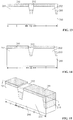
- Figure 4 is a three-dimensional view of the structure illustrated in the Figure 3 ; and the Figure 3 is a cross-sectional view of the structure illustrated in Figure 4 along the dashed line "A-a".
- a first gate structure (not shown) across the first fins 101 is formed on the semiconductor substrate 100.
- the first gate structure covers the side surfaces of the first fins 101.
- a second gate structure (not shown) across the second fins 102 is formed on the semiconductor substrate 100.
- the second gate structure covers the side surfaces of the second fins 102.
- first doped source/drain regions are formed in the first fins 101 at two sides of the first gate structure by an epitaxial growth process.
- Second doped source/drain regions are formed in the second fins 102 at two sides of the second gate structure by an epitaxial growth process.
- the isolation structure 110 is formed by the FCVD process.
- the FCVD process is able to allow the isolation structure 110 to fully fill the gaps between the adjacent first fins 101, the gaps between the adjacent second fins 102; and the gaps between the first fin 101 and the adjacent second fin 102.
- the compactness of the isolation structure 110 formed by the FCVD process is not as desired; and the isolations structure 110 is easy to be etched.
- the portion of the isolation structure 110 between the first fin 101 and the second fin 102 (the dashed region 1 illustrated in Figure 3 ) is easy to be etched; and the portion of the isolation structure 110 between the first fin 101 and the second fin 102 is easy to be etched through.
- the isolating property of the isolation structure 110 is reduced; and the properties of the semiconductor structure are easily affected.
- the isolation structure 110 between the first fin 101 and the second fin 102 is etched through, it is easy for the first doped source/drain regions and the second doped source/drain regions to connect with each other during the epitaxial process for forming the first doped source/drain regions and the second doped source/drain regions. Thus, the performance of the semiconductor structure is affected.
- the present invention provides a semiconductor structure and a fabrication method thereof.
- the fabrication method includes providing a semiconductor substrate having a first region, a second region, and an isolation region between the first region and the second region; forming a plurality of first fins on the semiconductor substrate in the first region and a plurality of second fins on the semiconductor substrate in the second region; forming an isolation structure covering the side surfaces of the first fins and the second fins and with a top surface below the top surfaces of the first fins and the second fins in the semiconductor substrate; and forming an isolation layer with the top surface above or level with the top surfaces of the first fins and the second fins on the isolation structure in the isolation region.
- the isolation structure Before forming the isolation layer, the isolation structure may be formed on the semiconductor substrate; and the top surface of the isolation structure may be below the top surfaces of the first fins and the second fins. During the process for forming the isolation layer, it may be unnecessary to perform an extra process to the isolation structure. Thus, the isolation structure may not be consumed; and the morphology and size of the isolation layer may be as desired. Accordingly, the isolation property of the isolation structure and the isolation layer may be improved; and the performance of the semiconductor structure may be enhanced.
- Figure 18 illustrates an exemplary fabrication of a semiconductor structure consistent with the disclosed embodiments.
- Figures 5-17 illustrate semiconductor structures corresponding to certain stages of the exemplary fabrication process.
- FIG. 18 As shown in Figure 18 , at the beginning of the fabrication process, a semiconductor substrate with certain structures is provided (S101).
- Figure 5 illustrates a corresponding semiconductor structure.
- a semiconductor substrate 200 is provided.
- the semiconductor substrate 200 may include a first region I, a second region II, and an isolation region III between the first region I and the second region II.
- a plurality of first fins 201 may be formed on the semiconductor substrate 200 in the first region I; and a plurality of second fins 202 may be formed on the semiconductor substrate 200 in the second region II.
- first fins 201 and the second fins 202 may be aligned along the extension direction of the first fins 201 and the second fins 202.
- the plurality of first fins 201 may be aligned along the direction perpendicular to the extension direction of the first fins 201.
- the plurality of second fins 202 may be aligned along the direction perpendicular to the extension direction of the second fins 202.
- the semiconductor substrate 200 is a silicon substrate.
- the semiconductor substrate may be a germanium substrate, a silicon germanium substrate, a silicon on insulator substrate, or a germanium on insulator substrate, etc.
- the first fins 201 and the second fins 202 are made of silicon. In some embodiments, the first fins 201 and the second fins 202 may be made of germanium or silicon germanium, etc.
- the method for forming the semiconductor substrate 200, the first fins 201 and the second fins 202 may include providing a base substrate; forming a patterned mask layer (not shown) on the base substrate; and etching the base substrate using the patterned mask layer as an etching mask.
- the mask layer may be made of any appropriate material.
- the mask layer is made of silicon nitride, or silicon oxynitride, etc.
- an isolation structure may be formed on the semiconductor substrate 200 (S102).
- Figures 6-8 illustrate structures corresponding to certain stages of the process for forming the isolation structure.
- Figure 8 is the 3D view of the structure illustrated Figure 7; and
- Figure 7 is a cross-sectional view of the structure illustrated in Figure 8 along the dashed line 1-2.
- an initial isolation structure 211 is formed on the semiconductor substrate 200.
- the initial isolation structure 211 may cover the side surfaces of the first fins 201 and the second fins 202.
- the top surface of the initial isolation structure 211 may be above, or level with (i.e., not below) the top surfaces of the first fins 201 and the second fins 202.
- the initial isolation structure 211 may be used to subsequently form an isolation structure.
- the initial isolation structure 211 may be made of silicon oxide.
- the initial isolation structure 211 may be made of silicon oxynitride.
- an FCVD process is used to form the initial isolation structure 211.
- the initial isolation structure 211 formed by the FCVD process may have a relatively strong filling ability to gaps between the first fins 201 and the adjacent second fins 202, the gaps between adjacent first fins 201, and the gaps between adjacent second fins 202.
- the isolation property of the subsequently formed isolation structure may be as desired.
- the initial isolation structure 211 may be etched to cause the top surface of the initial isolation structure 211 to be below the top surfaces of the first fins 201 and the second fins 202. Accordingly, the insolation structure 210 may be formed.
- the isolation structure 210 may be used to isolate the first fins 201 and the adjacent second fins 202; isolate the adjacent first fins 201; and isolate the adjacent second fins 202.
- the isolation structure 210 may also be referred to as a single diffusion break (SDB) structure
- the subsequently formed first gate structure may be able to cover the exposed portions of the side surfaces of the first fins 201.
- the subsequently formed second gate structure may be able to cover the exposed portions of the side surfaces of the second fins 202.
- the control ability of the first gate structure on the current inside the first fins 201 and the control ability of the second gate structure on the current inside the second fins 202 may be increased.
- the initial isolation structure 211 Before subsequently forming an isolation layer, the initial isolation structure 211 may be etched. The loss of the portion of the initial isolation structure 211 in the isolation region III caused by etching the initial isolation structure 211 may be subsequently compensated after forming the isolation layer. Thus, the reduction of the isolation ability of the portion of the isolation structure in the isolation region III caused by etching the initial isolation structure 211 may be prevented.
- the process for etching the initial isolation structure 211 to cause the portions of the initial isolation structure 211 between the adjacent first fins 201 to be below the top surfaces of the first fins 201 and to cause the portions of the initial isolation structure 211 between adjacent second fins 202 to be below the top surfaces of the second fins 202 may also cause the portion of the initial isolation structure 211 between the first fin 201 and the adjacent second fin 202 to be below the top surfaces of the first fins 201 and the second fins 202.
- the initial isolation structure 211 may be etched by any appropriate process, such as a dry etching process, or a wet etching process, etc. In one embodiment, a dry etching process is used to etch the initial isolation structure 211.
- An isolation layer may be subsequently formed on the portion of the isolation structure 210 in the isolation region III.
- the top surface of the isolation layer may be above or level with (i.e., not below) the top surfaces of the first fins 201 and the second fins 202.
- a sacrificial layer may be formed on portions of the isolation structure 210 in the first region I and the second region II (S103).
- Figures 9-11 illustrate structures corresponding to certain stages of the process for forming the sacrificial layer.
- an initial sacrificial layer 220 is formed on the isolation structure 210, the first fins 201 and the second fins 202.
- the initial sacrificial layer 220 may be used to subsequently form a sacrificial layer; and may also be used to protect the portions of the isolation structure 210 in the first region I and the second region II during the subsequent process for etching the isolation layer.
- the initial sacrificial layer 220 may also be on the top surfaces of the first fins 201 and the second fins 202.
- the portions of the initial sacrificial layer 220 on the first fins 201 and the second fins 202 may be used to protect the first fins 201 and the second fins 202 during the subsequent process for removing the initial isolation layer on the initial sacrificial layer 220.
- the initial sacrificial layer 220 may be made of any appropriate material.
- the initial sacrificial layer 220 is a spin-on carbon (SOC) layer.
- the initial sacrificial layer may be an organic dielectric layer.
- the spin-on carbon layer is a carbon-containing polymer.
- the carbon-containing polymer may contain a benzene ring and alkyl containing polymer.
- the mass percentile of carbon atoms in the initial sacrificial layer 220 may be in a range of approximately 85%-90%.
- the thickness of the initial sacrificial layer 220 may be in a range of approximately 1000 ⁇ -2000 ⁇ .
- the initial sacrificial layer 220 is formed by a spin-coating process.
- a bottom anti-reflective layer 232 may be formed on the initial sacrificial layer 220; a dielectric anti-reflective layer 231 may be formed on the bottom anti-reflective layer 232; and a patterning layer 230 may be formed on the dielectric anti-reflective layer 232.
- the patterning layer 203 may be formed on the initial sacrificial layer 220 over the first region I and the second region II; and may be used to protect the initial sacrificial layer 220 over the first fins 201 and the second fins 202 from being etched.
- the patterning layer 203 may have an opening (not labeled) over the portion of the isolation structure 210 in the isolation region III; and may be used to subsequently remove the portion of the initial sacrificial layer 220 in the isolation region III.
- the patterning layer 230 may be made of any appropriate material.
- the pattern layer 230 is a patterned photoresist layer.
- the bottom anti-reflective layer 232 and the dielectric anti-reflective layer 231 may be used to planarize the etching surface; and to reduce the light reflection of the etching surface.
- the bottom anti-reflective layer 232 may be made of any appropriate material. In one embodiment, the bottom anti-reflective layer 232 is made of organic material.
- the dielectric anti-reflective layer 231 may be made of any appropriate material.
- the dielectric layer anti-reflective layer 231 is made of silicon oxynitride.
- the initial sacrificial layer 220 may be etched using the patterning layer 230 as an etching mask. The portion of the initial sacrificial layer 220 on the isolation structure 210 in the isolation region III may be removed; and the sacrificial layer 241 may be formed.
- the sacrificial layer 241 may be used to protect the first fins 201, the second fins 202 and the isolation structure 210 during the subsequent process for removing the portion of an initial isolation layer on the sacrificial layer 241. Further, the sacrificial layer 241 may be also be able to prevent the portions of the isolation structure 210 in the first region I and the second region, and on the first fins 201 and the second fins 202 from being etched during the subsequent process for etching the isolation layer.
- the initial sacrificial layer 220 may be etched by any appropriate process.
- a dry etching process is used to each the initial sacrificial layer 220.
- the etching gases of the dry etching process may include O 2 , SO 2 and N 2 , etc.
- the pressure of the reaction chamber of the dry etching process may be in a range of approximately 5 m Torr-20 mTorr.
- the bias voltage may be in a range of approximately 100 V-500 V.
- the material of the sacrificial layer 241 may be identical to the material of the initial sacrificial layer 220.
- the initial sacrificial layer 241 may be a spin-on carbon layer.
- the sacrificial layer may be an organic dielectric layer.
- the thickness of the sacrificial layer 241 may be in a range of approximately 1000 ⁇ -2000 ⁇ .
- the patterning layer 230 (referring to Figure 10 ) may be removed. Then, the dielectric anti-reflective layer 231 (referring to Figure 10 ) may be removed; and the bottom anti-reflective layer 232 (referring to Figure 10 ) may be removed.
- an initial isolation layer may be formed (S104).
- Figure 12 illustrates a corresponding semiconductor structure.
- an initial isolation layer 250 is formed on the exposed portion of the isolation structure 210 and the sacrificial layer 241.
- the initial isolation layer 250 may be used to subsequently form an isolation layer.
- the initial isolation layer 250 may be made of any appropriate material. In one embodiment, the initial isolation layer 250 is made of silicon oxide.
- the initial isolation layer 250 may be formed by a high density plasma deposition process, or a high aspect ratio deposition process, etc.
- the initial isolation layer 250 formed by the high density plasma deposition process or the high aspect ratio deposition process may have a relatively high compactness, the material loss during the subsequent process for removing the sacrificial layer 241 may be relatively small.
- the isolation properties of the subsequently formed isolation layer may be as desired.
- an isolation layer may be formed (S105).
- Figure 13 illustrates a corresponding semiconductor structure.
- an isolation layer 252 is formed.
- the isolation layer 252 may be formed by removing the portion of the initial isolation layer 250 above the sacrificial layer 241.
- the isolation layer 252 may be used to isolate the subsequently formed first doped source/drain regions and the second doped source/drain regions; and prevent the first doped source/drain regions and the second doped source/drain regions from connecting together.
- the portion of the initial isolation layer 250 above the sacrificial layer 241 may be removed by any appropriate process.
- a chemical mechanical polishing process is used to remove the portion of the initial isolation layer 250 above the sacrificial layer 241 until the sacrificial layer 241 is exposed.
- Figures 14-15 illustrate a corresponding semiconductor structure.
- Figure 15 is a 3D view of the structure illustrated in Figure 14; and
- Figure 14 is a cross-sectional view of the structure illustrated in Figure 15 along the dashed line 3-4.
- the top surface of the isolation layer 252 may be recessed; and the top surface height, i.e., the height of the top surface the isolation layer 252 along the direction perpendicular to the semiconductor substrate 200, may be reduced. That is, the top surface of the isolation layer 252 may be below the top surface of the sacrificial layer 241.
- the purpose for etching the isolation layer 252 is to cause the height difference between the top surface of the isolation layer 252 and the top surfaces of the first fins 201 and the second fins 202 to match the design requirements.
- the top surface height of the isolation layer 252 is too large, it may be not good for subsequently forming a dummy gate structure. If the top surface height of the isolation layer 252 is too small, it may not be good for preventing the connection between the subsequently formed first doped source/drain regions and second doped source/drain regions. In one embodiment, the height difference between the top surface of the isolation layer 252 and the top surfaces of the first fins 201 and the second fins 202 may be in a range of approximately 200 ⁇ -800 ⁇ .
- the sacrificial layer 241 may cover the portions of the isolation structure 210 in the first region I and the second region II, during the process for etching the isolation layer 252, the sacrificial layer 241 may be able to protect the portions of the isolation structure 210 in the first region I and the second region II. Accordingly, it may prevent the portions of the isolation structure 210 in the first region I and the second region II from being etched. Further, because the sacrificial layer 241 may cover side surfaces of the initial isolation layer 250, the consumption of the side surfaces of the initial isolation layer 250 may be reduced.
- the isolation layer 252 may be etched by any appropriate process. In one embodiment, a dry etching process is used to etch the isolation layer 252. In some embodiments, a wet etching process may be used to etch the isolation layer.
- the process for etching the isolation layer may be omitted.
- the sacrificial layer 241 may be removed (S106).
- Figure 16 illustrates a corresponding semiconductor structure.
- the sacrificial layer 241 is removed.
- the first fins 201, the second fins 202 and the isolation layer 252 may be exposed.
- the isolation structure 210 and the isolation layer 252 may also be removed with a certain removing rate.
- the ratio between the removing rate of the sacrificial layer 241 and the removing rate of the isolation structure 210 may be any appropriate value. If the ratio between the removing rate of the sacrificial layer 241 and the removing rate of the isolation structure 210 is too small, it may cause the isolation structure 210 and the isolation layer 252 to be consumed too much; and the performance of the semiconductor structure may be deteriorated. Thus, the ratio between the removing rate of the sacrificial layer 241 and the removing rate of the isolation structure 210 should not be too small. In one embodiment, the ratio between the removing rate of the sacrificial layer 241 and the removing rate of the isolation structure 210 may be greater than 10.
- the sacrificial layer 241 may be removed by any appropriate process.
- the sacrificial layer 241 is a spin-on carbon layer, a plasma ashing process may be used to remove the sacrificial layer 341.
- the ratio between the removing rate of the sacrificial layer 241 and the removing rate of the isolation structure 210 may be relatively large.
- the consumption of the isolation structure 210 and the isolation layer 252 caused by the plasma ashing process may be relatively small.
- a first gate structure, a second gate structure, first doped source/drain regions and second doped source/drain regions may be formed (S107).
- Figure 17 illustrates a corresponding semiconductor structure.
- a first gate structure 271 crossing over the first fins 201 may be formed over the semiconductor substrate 200.
- the first gate structure 271 may cover portions of the side and top surfaces of the first fins 201.
- a second gate structure 272 crossing over the second fins 202 may be formed over the semiconductor substrate 200.
- the second gate structure 272 may cover portions of side and top surfaces of the second fins 202.
- first doped source/drain regions 261 may be formed in the first fins 201 at two sides of the first gate structure 271.
- Second doped source/drain regions 262 may be formed in the second fins 202 at two sides of the second gate structure 272.
- a dummy gate structure 270 may be formed on the isolation layer 252.
- the first doped source/drain regions 261 and the second doped source/drain regions 262 may be formed by any appropriate process. In one embodiment, epitaxial growth processes are used to form the first doped source/drain regions 261 and the second doped source/drain regions 262.
- the process for forming the first doped source/drain regions 261 and the second doped source/drain regions 262 may include forming first trenches in the first fins 201 at two sides of the first gate structure 271; forming second trenches in the second fins 202 at two sides of the second gate structure 272; forming the first doped source/drain regions 261 in the first trenches by an epitaxial growth process; and forming the second doped source/drain regions 262 in the second trenches by an epitaxial growth process.
- the isolation structure 210 and the isolation layer 252 may be between the first trenches and the adjacent second trenches; and the top surface of the isolation layer 252 and the top surfaces of the first fins 201 and the second fins 202 may have a certain height difference, the isolation layer 252 may be able to isolate the first trenches and the adjacent second trenches.
- the first doped source/drain regions 261 and the second doped source/drain regions 262 may not be easy to connect with each other during the epitaxial growth processes.
- the dummy gate structure 270 may be formed on the isolation layer 252 after forming the isolation layer 252.
- the dummy gate structure 270 may be used to protect the isolation layer 252 during the processes for forming the first trenches and the second trenches.
- a semiconductor structure may be formed by the disclosed methods and processes.
- Figure 17 illustrates a corresponding semiconductor structure.
- the semiconductor structure may include a semiconductor substrate 200 having a first region I, a second region II and an isolation region III between the first region I and the second region II; a plurality of first fins 201 formed on the semiconductor substrate 200 in the first region I; and a plurality of second fins 202 formed on the semiconductor substrate 200 in the second region II.
- the semiconductor structure may also include an isolation structure 210 formed on the semiconductor substrate 200 and covering portions of the side surfaces of the first fins 201 and the second fins 202; and an isolation layer 252 formed on the portion of the isolation structure 210 in the isolation region III.
- the semiconductor structure may include a first gate structure 271 crossing over the first fins 201 and covering portions of the side and top surfaces of the first fins 201 formed on the semiconductor substrate 200 in the first region I; a second gate structure 272 crossing over the second fins 202 and covering portions of the side and top surfaces of the second fins 202 formed on the semiconductor substrate 200 in the second region II; and a dummy gate structure 270 formed on the isolation layer 252.
- the semiconductor structure may also include first doped source/drain regions 261 formed in the first fins 201 at two sides of the first gate structure 271; and second doped source/drain regions 262 formed in the second fins 202 at two sides of the second gate structure 272.
- an isolation structure may be formed on the semiconductor substrate; and the top surface of the isolation structure is below the top surfaces of the first fins and the second fins.
- the isolation structure may not need to be treated.
- the isolation structure may not be easily consumed and the morphology and size of the isolation layer may be as desired.
- the isolation property of the isolation structure and the isolation layer may be improved; and the performance of the semiconductor structure may be improved.
- the sacrificial layer may cover the surfaces of the portions of the isolation structure in the first region and the second region and the side surfaces of a portion of the isolation layer.
- the sacrificial layer may be formed on the top surfaces of the first fins and the second fins.
- the sacrificial layer may be able to protect the isolation structure, the first fins and the second fins during the process for removing the portion of the initial isolation layer on the sacrificial layer.
- the sacrificial layer may also be able to protect the portions of the isolation structure in the first region and the second region during the process for etching the isolation layer.
- the isolation property of the portion of the isolation structure in the isolation region may be improved.
- the sacrificial layer may be a spin-on carbon layer, or an organic dielectric layer; and may be removed by a plasma ashing process.
- the removing rate of the plasma ashing process to the isolation layer may be significantly smaller than the removing rate of the plasma ashing process to the sacrificial layer.
- the consumption of the isolation structure may be relatively small. Accordingly, the property of the semiconductor structure may be improved.
- the isolation layer may be formed between the first fins and the second fins; and the top surface of the isolation layer may be above the top surfaces of the first fins and the second fins.
Landscapes
- Engineering & Computer Science (AREA)
- Power Engineering (AREA)
- Microelectronics & Electronic Packaging (AREA)
- Physics & Mathematics (AREA)
- Condensed Matter Physics & Semiconductors (AREA)
- General Physics & Mathematics (AREA)
- Computer Hardware Design (AREA)
- Manufacturing & Machinery (AREA)
- Ceramic Engineering (AREA)
- Insulated Gate Type Field-Effect Transistor (AREA)
- Element Separation (AREA)
Abstract
Description
- This application claims the priority of Chinese patent application No.
201610744286.3, filed on August 26, 2016 - The present invention generally relates to the field of semiconductor manufacturing technology and, more particularly, relates to semiconductor structures and fabrication methods thereof.
- With the continuous increase of the integration level of semiconductor devices, the critical dimension (CD) of transistors has become smaller and smaller. With the rapid shrinking of the size of the transistors, the thickness of the gate dielectric layer and the working voltage of the transistors are unable to correspondingly change. Thus, the difficulty for preventing the short channel effect is increased; and the leakage current of the transistor is increased.
- The fins of fin field-effect transistors (FinFETs) form fork-like three-dimensional (3D) structures like fishes' fins. The channel regions of the FinFETs protrude from the surface of the substrate to form the fins. The gate structures of the FinFETs cover the top and side surfaces of the fins. Thus, the reverse type layers are formed on all sides of the channel regions. Correspondingly, the gate structures are able to control the "on" and "off" of control circuits from two sides of the fins. Such a design (device structure) is able to increase the control ability of the gate structures to the channel regions; and is able to effectively suppress the short channel effect of the FinFETs.
- To isolate adjacent fins, before forming the doped source/drain regions, isolation structures are formed in the substrate between adjacent fins. The isolation structures between the doped source/drain regions in different fins need to have a certain height. If the heights of the isolation structures between the doped source/drain regions in different fins are too small, the doped source/drain regions may be easy to connect together; and the performance of the FinFETs are easily affected.
- It is an object of the present invention to provide a semiconductor structure, such as a FinFET, and a method for fabricating the same which may solve one or more problems set forth above and other problems in the art in which the risk of a connection between doped source/drain regions is avoided or at least reduced so that the performance of the FinFET can be improved.
- A first aspect of the present invention provides a method for fabricating a semiconductor structure.
- The fabrication method includes providing a semiconductor substrate having a first region, a second region and an isolation region between the first region and the second region; forming a plurality of first fins on the semiconductor substrate in the first region and a plurality of second fins on the semiconductor substrate in the second region; forming an isolation structure, covering portions of side surfaces of the first fins and the second fins and with a top surface below the top surfaces of the first fins and the second fins, over the semiconductor substrate; and forming an isolation layer over the isolation structure in the isolation region and with a top surface coplanar or above the top surfaces of the first fins and the second fins.
- Preferably, forming the isolation layer comprises: forming a sacrificial layer over the isolation structure, the first fins and the second fins and exposing a portion of the isolation structure in the isolation region; forming an initial isolation layer on exposed portion of the isolation structure and on the sacrificial layer; removing a portion of the initial isolation layer on the sacrificial layer; and removing the sacrificial layer.
- Preferably, the sacrificial layer is one of a spin-on carbon layer and an organic dielectric layer.
- Preferably, the spin-on carbon layer is made of carbon-containing polymer.
- Preferably, a mass percentile of carbon atoms in the spin-on carbon layer is in a range of approximately 85%-90%.
- Preferably, a thickness of the sacrificial layer is in a range of approximately 1000Å-2000Å.
- Preferably, forming the sacrificial layer comprises: forming an initial sacrificial layer on the isolation structure, the first fins and the second fins; and removing a portion of the initial sacrificial layer on the portion of the isolation structure in the isolation region.
- Preferably, a ratio between a removing rate of the sacrificial layer and a removing rate of the isolation structure is greater than approximately 10.
- Preferably, the sacrificial layer being one of a spin-on carbon layer and an organic dielectric layer, wherein: the sacrificial layer is removed by a plasma ashing process.
- Preferably, forming the isolation layer further comprises: etching the isolation layer using the sacrificial layer as an etching mask after removing the portion of the initial isolation layer on the sacrificial layer.
- Preferably, forming the isolation structure comprises: forming an initial isolation structure covering side surfaces of the first fins and the second fins and with a top surface not below top surfaces of the first fins and the second fins; and etching the initial isolation structure to cause the top surface of the isolation structure to be below the first fins and the second fins.
- Preferably, the initial isolation structure is formed by a flowable chemical vapor deposition process.
- Preferably, after forming the isolation layer, further comprising: forming a first gate structure over the semiconductor substrate and across the first fins by covering top and side surfaces of the first fins; forming a second gate structure over the semiconductor substrate and across the second fins by covering top and side surfaces of the second fins; forming first doped source/drain regions in the first fins at two sides of the first gate structure; and forming second doped source/drain regions in the second fins at two sides of the second gate structure, wherein the first doped source/drain regions and the second doped source/drain regions are at two sides of the isolation layer.
- Preferably, the first doped source/drain regions and the second doped source/drain regions are formed by epitaxial growth processes.
- Preferably, after forming the isolation layer, further comprising: forming a dummy gate structure on the isolation layer.
- A second aspect of the present invention provides a semiconductor structure.
- The semiconductor structure may include a semiconductor substrate having a first region, a second region and an isolation region between the first region and the second region; a plurality of first fins formed on the semiconductor substrate in the first region and a plurality of second fins formed on the semiconductor substrate in the second region; an isolation structure covering portions of the side surfaces of the first fins and the second fins formed on the semiconductor substrate; an isolation layer formed on a portion of the isolation structure in the isolation region; a first gate structure formed on the semiconductor substrate in the first region and across the first fins by covering portions of the side and top surfaces of the first fins; a second gate structure formed on the semiconductor substrate in the second region and across the second fins by covering portions of side and top surfaces of the second fins; first doped source/drain regions formed in the first fins at two sides of the first gate structure; and second doped source/drain regions formed in the second fins at two sides of the second gate structure.
- Preferably, a top surface of the isolation layer is above the top surfaces of the first fins and the second fins.
- Preferably, a surface height difference between the top surface of the isolation layer and the top surfaces of the first fins and the second fins is in a range of approximately 200Å-800Å.
- Preferably, the semiconductor structure further comprises a dummy gate structure formed on the isolation layer.
- Preferably, the isolation layer is between the first fins and the second fins.
- A semiconductor structure according to the second aspect of the present invention may be obtained by a method according to the first aspect of the present invention.
- Other aspects of the present invention can be understood by those skilled in the art in light of the description, the claims, and the drawings of the present invention.
-
-
Figures 1-4 illustrate structures corresponding to certain stages of a fabrication process of a semiconductor structure; -
Figures 5-17 illustrate structures corresponding to certain stages of a fabrication process of an exemplary semiconductor structure consistent with the disclosed embodiments; and -
Figure 18 illustrates an exemplary fabrication process of a semiconductor structure consistent with the disclosed embodiments. - Reference will now be made in detail to exemplary embodiments of the disclosure, which are illustrated in the accompanying drawings. Wherever possible, the same reference numbers will be used throughout the drawings to refer to the same or like parts.
-
Figures 1-4 illustrate structures corresponding to certain stages of a fabrication method of a semiconductor structure. As shown inFigure 1 , the fabrication method includes providing a base substrate. The base substrate includes asemiconductor substrate 100 and a plurality offirst fins 101 and a plurality ofsecond fins 102 on thesemiconductor substrate 100. - The method also includes forming an
isolation structure 110 on thesemiconductor substrate 100 by a flowable chemical vapor deposition (FCVD) process. Theisolation structure 110 covers the side surfaces of thefirst fins 101 and thesecond fins 102. The top surface of theisolation structure 110 levels with the top surfaces of thefirst fins 101 and thesecond fins 102. - Further, as shown in
Figure 2 , the method includes forming anisolation layer 120 on theisolation structure 110 between thefirst fins 101 and thesecond fins 102. - Further, as shown in
Figures 3-4 , the method includes etching theisolation structure 110 and theisolation layer 120 to cause the surface of theisolation structure 110 to be below the top surfaces of thefins 101 and thesecond fins 102; and to reduce the height of theisolation layer 120.Figure 4 is a three-dimensional view of the structure illustrated in theFigure 3 ; and theFigure 3 is a cross-sectional view of the structure illustrated inFigure 4 along the dashed line "A-a". - Further, a first gate structure (not shown) across the
first fins 101 is formed on thesemiconductor substrate 100. The first gate structure covers the side surfaces of thefirst fins 101. A second gate structure (not shown) across thesecond fins 102 is formed on thesemiconductor substrate 100. The second gate structure covers the side surfaces of thesecond fins 102. - Further, first doped source/drain regions (not shown) are formed in the
first fins 101 at two sides of the first gate structure by an epitaxial growth process. Second doped source/drain regions (not shown) are formed in thesecond fins 102 at two sides of the second gate structure by an epitaxial growth process. - In the process for forming the semiconductor structure, the
isolation structure 110 is formed by the FCVD process. The FCVD process is able to allow theisolation structure 110 to fully fill the gaps between the adjacentfirst fins 101, the gaps between the adjacentsecond fins 102; and the gaps between thefirst fin 101 and the adjacentsecond fin 102. - However, the compactness of the
isolation structure 110 formed by the FCVD process is not as desired; and theisolations structure 110 is easy to be etched. During the process for etching theisolation structure 110, the portion of theisolation structure 110 between thefirst fin 101 and the second fin 102 (the dashedregion 1 illustrated inFigure 3 ) is easy to be etched; and the portion of theisolation structure 110 between thefirst fin 101 and thesecond fin 102 is easy to be etched through. Thus, the isolating property of theisolation structure 110 is reduced; and the properties of the semiconductor structure are easily affected. - Further, if the
isolation structure 110 between thefirst fin 101 and thesecond fin 102 is etched through, it is easy for the first doped source/drain regions and the second doped source/drain regions to connect with each other during the epitaxial process for forming the first doped source/drain regions and the second doped source/drain regions. Thus, the performance of the semiconductor structure is affected. - The present invention provides a semiconductor structure and a fabrication method thereof. The fabrication method includes providing a semiconductor substrate having a first region, a second region, and an isolation region between the first region and the second region; forming a plurality of first fins on the semiconductor substrate in the first region and a plurality of second fins on the semiconductor substrate in the second region; forming an isolation structure covering the side surfaces of the first fins and the second fins and with a top surface below the top surfaces of the first fins and the second fins in the semiconductor substrate; and forming an isolation layer with the top surface above or level with the top surfaces of the first fins and the second fins on the isolation structure in the isolation region.
- Before forming the isolation layer, the isolation structure may be formed on the semiconductor substrate; and the top surface of the isolation structure may be below the top surfaces of the first fins and the second fins. During the process for forming the isolation layer, it may be unnecessary to perform an extra process to the isolation structure. Thus, the isolation structure may not be consumed; and the morphology and size of the isolation layer may be as desired. Accordingly, the isolation property of the isolation structure and the isolation layer may be improved; and the performance of the semiconductor structure may be enhanced.
-
Figure 18 illustrates an exemplary fabrication of a semiconductor structure consistent with the disclosed embodiments.Figures 5-17 illustrate semiconductor structures corresponding to certain stages of the exemplary fabrication process. - As shown in
Figure 18 , at the beginning of the fabrication process, a semiconductor substrate with certain structures is provided (S101).Figure 5 illustrates a corresponding semiconductor structure. - As shown in
Figure 5 , asemiconductor substrate 200 is provided. Thesemiconductor substrate 200 may include a first region I, a second region II, and an isolation region III between the first region I and the second region II. A plurality offirst fins 201 may be formed on thesemiconductor substrate 200 in the first region I; and a plurality ofsecond fins 202 may be formed on thesemiconductor substrate 200 in the second region II. - In one embodiment, the
first fins 201 and thesecond fins 202 may be aligned along the extension direction of thefirst fins 201 and thesecond fins 202. The plurality offirst fins 201 may be aligned along the direction perpendicular to the extension direction of thefirst fins 201. The plurality ofsecond fins 202 may be aligned along the direction perpendicular to the extension direction of thesecond fins 202. - In one embodiment, the
semiconductor substrate 200 is a silicon substrate. In some embodiments, the semiconductor substrate may be a germanium substrate, a silicon germanium substrate, a silicon on insulator substrate, or a germanium on insulator substrate, etc. - In one embodiment, the
first fins 201 and thesecond fins 202 are made of silicon. In some embodiments, thefirst fins 201 and thesecond fins 202 may be made of germanium or silicon germanium, etc. - In one embodiment, the method for forming the
semiconductor substrate 200, thefirst fins 201 and thesecond fins 202 may include providing a base substrate; forming a patterned mask layer (not shown) on the base substrate; and etching the base substrate using the patterned mask layer as an etching mask. - The mask layer may be made of any appropriate material. In one embodiment, the mask layer is made of silicon nitride, or silicon oxynitride, etc.
- Returning to
Figure 18 , after providing thesemiconductor substrate 200 having the fins, an isolation structure may be formed on the semiconductor substrate 200 (S102).Figures 6-8 illustrate structures corresponding to certain stages of the process for forming the isolation structure.Figure 8 is the 3D view of the structure illustratedFigure 7; and Figure 7 is a cross-sectional view of the structure illustrated inFigure 8 along the dashed line 1-2. - As shown in
Figure 6 , aninitial isolation structure 211 is formed on thesemiconductor substrate 200. Theinitial isolation structure 211 may cover the side surfaces of thefirst fins 201 and thesecond fins 202. The top surface of theinitial isolation structure 211 may be above, or level with (i.e., not below) the top surfaces of thefirst fins 201 and thesecond fins 202. - The
initial isolation structure 211 may be used to subsequently form an isolation structure. In one embodiment, theinitial isolation structure 211 may be made of silicon oxide. In some embodiments, theinitial isolation structure 211 may be made of silicon oxynitride. - Various processes may be used to form the
initial isolation structure 211. In one embodiment, an FCVD process is used to form theinitial isolation structure 211. Theinitial isolation structure 211 formed by the FCVD process may have a relatively strong filling ability to gaps between thefirst fins 201 and the adjacentsecond fins 202, the gaps between adjacentfirst fins 201, and the gaps between adjacentsecond fins 202. The isolation property of the subsequently formed isolation structure may be as desired. - After forming the
initial isolation structure 211, as shown inFigures 7-8 , theinitial isolation structure 211 may be etched to cause the top surface of theinitial isolation structure 211 to be below the top surfaces of thefirst fins 201 and thesecond fins 202. Accordingly, theinsolation structure 210 may be formed. - The
isolation structure 210 may be used to isolate thefirst fins 201 and the adjacentsecond fins 202; isolate the adjacentfirst fins 201; and isolate the adjacentsecond fins 202. Theisolation structure 210 may also be referred to as a single diffusion break (SDB) structure - After etching the
initial gate structure 211 to cause the top surface of theinitial isolation structure 211 to be below the top surfaces of thefirst fins 201 and thesecond fins 202, top portions of the side surfaces of thefirst fins 201 and thesecond fins 202 may be exposed. Thus, the subsequently formed first gate structure may be able to cover the exposed portions of the side surfaces of thefirst fins 201. Similarly, the subsequently formed second gate structure may be able to cover the exposed portions of the side surfaces of thesecond fins 202. Thus, the control ability of the first gate structure on the current inside thefirst fins 201 and the control ability of the second gate structure on the current inside thesecond fins 202 may be increased. - Before subsequently forming an isolation layer, the
initial isolation structure 211 may be etched. The loss of the portion of theinitial isolation structure 211 in the isolation region III caused by etching theinitial isolation structure 211 may be subsequently compensated after forming the isolation layer. Thus, the reduction of the isolation ability of the portion of the isolation structure in the isolation region III caused by etching theinitial isolation structure 211 may be prevented. - In one embodiment, the process for etching the
initial isolation structure 211 to cause the portions of theinitial isolation structure 211 between the adjacentfirst fins 201 to be below the top surfaces of thefirst fins 201 and to cause the portions of theinitial isolation structure 211 between adjacentsecond fins 202 to be below the top surfaces of thesecond fins 202 may also cause the portion of theinitial isolation structure 211 between thefirst fin 201 and the adjacentsecond fin 202 to be below the top surfaces of thefirst fins 201 and thesecond fins 202. - The
initial isolation structure 211 may be etched by any appropriate process, such as a dry etching process, or a wet etching process, etc. In one embodiment, a dry etching process is used to etch theinitial isolation structure 211. - An isolation layer may be subsequently formed on the portion of the
isolation structure 210 in the isolation region III. The top surface of the isolation layer may be above or level with (i.e., not below) the top surfaces of thefirst fins 201 and thesecond fins 202. - Returning to
Figure 18 , after etching theinitial isolation structure 211 to form theisolation structure 210, a sacrificial layer may be formed on portions of theisolation structure 210 in the first region I and the second region II (S103).Figures 9-11 illustrate structures corresponding to certain stages of the process for forming the sacrificial layer. - As shown in
Figure 9 , an initialsacrificial layer 220 is formed on theisolation structure 210, thefirst fins 201 and thesecond fins 202. The initialsacrificial layer 220 may be used to subsequently form a sacrificial layer; and may also be used to protect the portions of theisolation structure 210 in the first region I and the second region II during the subsequent process for etching the isolation layer. - In one embodiment, the initial
sacrificial layer 220 may also be on the top surfaces of thefirst fins 201 and thesecond fins 202. The portions of the initialsacrificial layer 220 on thefirst fins 201 and thesecond fins 202 may be used to protect thefirst fins 201 and thesecond fins 202 during the subsequent process for removing the initial isolation layer on the initialsacrificial layer 220. - The initial
sacrificial layer 220 may be made of any appropriate material. In one embodiment, the initialsacrificial layer 220 is a spin-on carbon (SOC) layer. In some embodiments, the initial sacrificial layer may be an organic dielectric layer. - In one embodiment, the spin-on carbon layer is a carbon-containing polymer. Specifically, the carbon-containing polymer may contain a benzene ring and alkyl containing polymer. The mass percentile of carbon atoms in the initial
sacrificial layer 220 may be in a range of approximately 85%-90%. - If the thickness of the initial
sacrificial layer 220 is too small, the subsequent protection function to thefirst fins 201, thesecond fins 202 and theisolation structure 210 may be relatively weak. If the thickness of the initialsacrificial layer 220 is too large, it may be easy to increase the difficulty for subsequently etching the initialsacrificial layer 220. Thus, the thickness of the initialsacrificial layer 220 may be in a range of approximately 1000Å-2000Å. - Various processes may be used to form the initial
sacrificial layer 220. In one embodiment, the initialsacrificial layer 220 is formed by a spin-coating process. - Further, as shown in
Figures 10 , after forming the initialsacrificial layer 220, a bottomanti-reflective layer 232 may be formed on the initialsacrificial layer 220; a dielectricanti-reflective layer 231 may be formed on the bottomanti-reflective layer 232; and apatterning layer 230 may be formed on the dielectricanti-reflective layer 232. - The patterning layer 203 may be formed on the initial
sacrificial layer 220 over the first region I and the second region II; and may be used to protect the initialsacrificial layer 220 over thefirst fins 201 and thesecond fins 202 from being etched. The patterning layer 203 may have an opening (not labeled) over the portion of theisolation structure 210 in the isolation region III; and may be used to subsequently remove the portion of the initialsacrificial layer 220 in the isolation region III. - The
patterning layer 230 may be made of any appropriate material. In one embodiment, thepattern layer 230 is a patterned photoresist layer. - In one embodiment, the bottom
anti-reflective layer 232 and the dielectricanti-reflective layer 231 may be used to planarize the etching surface; and to reduce the light reflection of the etching surface. - The bottom
anti-reflective layer 232 may be made of any appropriate material. In one embodiment, the bottomanti-reflective layer 232 is made of organic material. - The dielectric
anti-reflective layer 231 may be made of any appropriate material. In one embodiment, the dielectric layeranti-reflective layer 231 is made of silicon oxynitride. - After forming the
patterning layer 230, as shown inFigure 11 , the initialsacrificial layer 220 may be etched using thepatterning layer 230 as an etching mask. The portion of the initialsacrificial layer 220 on theisolation structure 210 in the isolation region III may be removed; and thesacrificial layer 241 may be formed. - The
sacrificial layer 241 may be used to protect thefirst fins 201, thesecond fins 202 and theisolation structure 210 during the subsequent process for removing the portion of an initial isolation layer on thesacrificial layer 241. Further, thesacrificial layer 241 may be also be able to prevent the portions of theisolation structure 210 in the first region I and the second region, and on thefirst fins 201 and thesecond fins 202 from being etched during the subsequent process for etching the isolation layer. - The initial
sacrificial layer 220 may be etched by any appropriate process. In one embodiment, a dry etching process is used to each the initialsacrificial layer 220. The etching gases of the dry etching process may include O2, SO2 and N2, etc. - In one embodiment, the pressure of the reaction chamber of the dry etching process may be in a range of approximately 5 m Torr-20 mTorr. The bias voltage may be in a range of approximately 100 V-500 V.
- In one embodiment, the material of the
sacrificial layer 241 may be identical to the material of the initialsacrificial layer 220. Specifically, the initialsacrificial layer 241 may be a spin-on carbon layer. In some embodiments, the sacrificial layer may be an organic dielectric layer. - In one embodiment, the thickness of the
sacrificial layer 241 may be in a range of approximately 1000Å-2000Å. - Further, as shown in
Figure 11 , after forming thesacrificial layer 241, the patterning layer 230 (referring toFigure 10 ) may be removed. Then, the dielectric anti-reflective layer 231 (referring toFigure 10 ) may be removed; and the bottom anti-reflective layer 232 (referring toFigure 10 ) may be removed. - Returning to
Figure 18 , after forming thesacrificial layer 241, an initial isolation layer may be formed (S104).Figure 12 illustrates a corresponding semiconductor structure. - As shown in
Figure 12 , aninitial isolation layer 250 is formed on the exposed portion of theisolation structure 210 and thesacrificial layer 241. Theinitial isolation layer 250 may be used to subsequently form an isolation layer. - The
initial isolation layer 250 may be made of any appropriate material. In one embodiment, theinitial isolation layer 250 is made of silicon oxide. - Various processes may be used to form the
initial isolation layer 250, such as a high density plasma deposition process, or a high aspect ratio deposition process, etc. Theinitial isolation layer 250 formed by the high density plasma deposition process or the high aspect ratio deposition process may have a relatively high compactness, the material loss during the subsequent process for removing thesacrificial layer 241 may be relatively small. Thus, the isolation properties of the subsequently formed isolation layer may be as desired. - Returning to
Figure 18 , after forming theinitial isolation layer 250, an isolation layer may be formed (S105).Figure 13 illustrates a corresponding semiconductor structure. - As shown in
Figure 13 , anisolation layer 252 is formed. Theisolation layer 252 may be formed by removing the portion of theinitial isolation layer 250 above thesacrificial layer 241. - The
isolation layer 252 may be used to isolate the subsequently formed first doped source/drain regions and the second doped source/drain regions; and prevent the first doped source/drain regions and the second doped source/drain regions from connecting together. - The portion of the
initial isolation layer 250 above thesacrificial layer 241 may be removed by any appropriate process. In one embodiment, a chemical mechanical polishing process is used to remove the portion of theinitial isolation layer 250 above thesacrificial layer 241 until thesacrificial layer 241 is exposed. - In one embodiment, after forming the
isolation layer 252, the top surface height of theisolation layer 252 may be reduced.Figures 14-15 illustrate a corresponding semiconductor structure.Figure 15 is a 3D view of the structure illustrated inFigure 14; and Figure 14 is a cross-sectional view of the structure illustrated inFigure 15 along the dashed line 3-4. - As shown in
Figures 14-15 , the top surface of theisolation layer 252 may be recessed; and the top surface height, i.e., the height of the top surface theisolation layer 252 along the direction perpendicular to thesemiconductor substrate 200, may be reduced. That is, the top surface of theisolation layer 252 may be below the top surface of thesacrificial layer 241. - The purpose for etching the
isolation layer 252 is to cause the height difference between the top surface of theisolation layer 252 and the top surfaces of thefirst fins 201 and thesecond fins 202 to match the design requirements. - If the top surface height of the
isolation layer 252 is too large, it may be not good for subsequently forming a dummy gate structure. If the top surface height of theisolation layer 252 is too small, it may not be good for preventing the connection between the subsequently formed first doped source/drain regions and second doped source/drain regions. In one embodiment, the height difference between the top surface of theisolation layer 252 and the top surfaces of thefirst fins 201 and thesecond fins 202 may be in a range of approximately 200Å-800Å. - Because the
sacrificial layer 241 may cover the portions of theisolation structure 210 in the first region I and the second region II, during the process for etching theisolation layer 252, thesacrificial layer 241 may be able to protect the portions of theisolation structure 210 in the first region I and the second region II. Accordingly, it may prevent the portions of theisolation structure 210 in the first region I and the second region II from being etched. Further, because thesacrificial layer 241 may cover side surfaces of theinitial isolation layer 250, the consumption of the side surfaces of theinitial isolation layer 250 may be reduced. - The
isolation layer 252 may be etched by any appropriate process. In one embodiment, a dry etching process is used to etch theisolation layer 252. In some embodiments, a wet etching process may be used to etch the isolation layer. - In some embodiments, after removing the portion of the initial isolation layer above the sacrificial layer, if the height difference between the top surface of the initial isolation layer on the isolation structure and the top surfaces of the first fins and the second fins matches the designed requirement, the process for etching the isolation layer may be omitted.
- Returning to
Figure 18 , after removing the portion of theinitial layer 250 on the sacrificial layer 241 (referring toFigure 13 and Figure 15 ), thesacrificial layer 241 may be removed (S106).Figure 16 illustrates a corresponding semiconductor structure. - As shown in
Figure 16 , thesacrificial layer 241 is removed. Thefirst fins 201, thesecond fins 202 and theisolation layer 252 may be exposed. - During the process for removing the
sacrificial layer 241, theisolation structure 210 and theisolation layer 252 may also be removed with a certain removing rate. The ratio between the removing rate of thesacrificial layer 241 and the removing rate of theisolation structure 210 may be any appropriate value. If the ratio between the removing rate of thesacrificial layer 241 and the removing rate of theisolation structure 210 is too small, it may cause theisolation structure 210 and theisolation layer 252 to be consumed too much; and the performance of the semiconductor structure may be deteriorated. Thus, the ratio between the removing rate of thesacrificial layer 241 and the removing rate of theisolation structure 210 should not be too small. In one embodiment, the ratio between the removing rate of thesacrificial layer 241 and the removing rate of theisolation structure 210 may be greater than 10. - The
sacrificial layer 241 may be removed by any appropriate process. In one embodiment, thesacrificial layer 241 is a spin-on carbon layer, a plasma ashing process may be used to remove the sacrificial layer 341. - In one embodiment, during the plasma ashing process for removing the
sacrificial layer 241, the ratio between the removing rate of thesacrificial layer 241 and the removing rate of theisolation structure 210 may be relatively large. The consumption of theisolation structure 210 and theisolation layer 252 caused by the plasma ashing process may be relatively small. - Returning to
Figure 18 , after removing thesacrificial layer 241, a first gate structure, a second gate structure, first doped source/drain regions and second doped source/drain regions may be formed (S107).Figure 17 illustrates a corresponding semiconductor structure. - As shown in
Figure 17 , afirst gate structure 271 crossing over thefirst fins 201 may be formed over thesemiconductor substrate 200. Thefirst gate structure 271 may cover portions of the side and top surfaces of thefirst fins 201. Asecond gate structure 272 crossing over thesecond fins 202 may be formed over thesemiconductor substrate 200. Thesecond gate structure 272 may cover portions of side and top surfaces of thesecond fins 202. - Further, first doped source/
drain regions 261 may be formed in thefirst fins 201 at two sides of thefirst gate structure 271. Second doped source/drain regions 262 may be formed in thesecond fins 202 at two sides of thesecond gate structure 272. - Further, as shown in
Figure 17 , in some embodiments, adummy gate structure 270 may be formed on theisolation layer 252. - The first doped source/
drain regions 261 and the second doped source/drain regions 262 may be formed by any appropriate process. In one embodiment, epitaxial growth processes are used to form the first doped source/drain regions 261 and the second doped source/drain regions 262. - Specifically, the process for forming the first doped source/
drain regions 261 and the second doped source/drain regions 262 may include forming first trenches in thefirst fins 201 at two sides of thefirst gate structure 271; forming second trenches in thesecond fins 202 at two sides of thesecond gate structure 272; forming the first doped source/drain regions 261 in the first trenches by an epitaxial growth process; and forming the second doped source/drain regions 262 in the second trenches by an epitaxial growth process. - Because the
isolation structure 210 and theisolation layer 252 may be between the first trenches and the adjacent second trenches; and the top surface of theisolation layer 252 and the top surfaces of thefirst fins 201 and thesecond fins 202 may have a certain height difference, theisolation layer 252 may be able to isolate the first trenches and the adjacent second trenches. Thus, the first doped source/drain regions 261 and the second doped source/drain regions 262 may not be easy to connect with each other during the epitaxial growth processes. - The
dummy gate structure 270 may be formed on theisolation layer 252 after forming theisolation layer 252. Thedummy gate structure 270 may be used to protect theisolation layer 252 during the processes for forming the first trenches and the second trenches. - Thus, a semiconductor structure may be formed by the disclosed methods and processes.
Figure 17 illustrates a corresponding semiconductor structure. - As shown in
Figure 17 , the semiconductor structure may include asemiconductor substrate 200 having a first region I, a second region II and an isolation region III between the first region I and the second region II; a plurality offirst fins 201 formed on thesemiconductor substrate 200 in the first region I; and a plurality ofsecond fins 202 formed on thesemiconductor substrate 200 in the second region II. The semiconductor structure may also include anisolation structure 210 formed on thesemiconductor substrate 200 and covering portions of the side surfaces of thefirst fins 201 and thesecond fins 202; and anisolation layer 252 formed on the portion of theisolation structure 210 in the isolation region III. Further, the semiconductor structure may include afirst gate structure 271 crossing over thefirst fins 201 and covering portions of the side and top surfaces of thefirst fins 201 formed on thesemiconductor substrate 200 in the first region I; asecond gate structure 272 crossing over thesecond fins 202 and covering portions of the side and top surfaces of thesecond fins 202 formed on thesemiconductor substrate 200 in the second region II; and adummy gate structure 270 formed on theisolation layer 252. Further, the semiconductor structure may also include first doped source/drain regions 261 formed in thefirst fins 201 at two sides of thefirst gate structure 271; and second doped source/drain regions 262 formed in thesecond fins 202 at two sides of thesecond gate structure 272. The detailed structures and intermediate structures are described above with respect to the fabrication processes. - Thus, according to the disclosed embodiments, before forming the isolation layer, an isolation structure may be formed on the semiconductor substrate; and the top surface of the isolation structure is below the top surfaces of the first fins and the second fins. During the process for forming the isolation layer, the isolation structure may not need to be treated. Thus, the isolation structure may not be easily consumed and the morphology and size of the isolation layer may be as desired. Thus, the isolation property of the isolation structure and the isolation layer may be improved; and the performance of the semiconductor structure may be improved.
- Further, the sacrificial layer may cover the surfaces of the portions of the isolation structure in the first region and the second region and the side surfaces of a portion of the isolation layer. Thus, the during the process for etching the initial isolation layer, it may not be easy to consume the portions of the isolation structure in the first region and the second region and the side surfaces of the isolation layer. Accordingly, the isolation property of the isolation structure and the isolation layer in the isolation region may be improved.
- Further, before forming the initial isolation layer, the sacrificial layer may be formed on the top surfaces of the first fins and the second fins. The sacrificial layer may be able to protect the isolation structure, the first fins and the second fins during the process for removing the portion of the initial isolation layer on the sacrificial layer. The sacrificial layer may also be able to protect the portions of the isolation structure in the first region and the second region during the process for etching the isolation layer. Thus, the isolation property of the portion of the isolation structure in the isolation region may be improved.
- Further, the sacrificial layer may be a spin-on carbon layer, or an organic dielectric layer; and may be removed by a plasma ashing process. The removing rate of the plasma ashing process to the isolation layer may be significantly smaller than the removing rate of the plasma ashing process to the sacrificial layer. Thus, during the process for removing the sacrificial layer, the consumption of the isolation structure may be relatively small. Accordingly, the property of the semiconductor structure may be improved.
- Further, the isolation layer may be formed between the first fins and the second fins; and the top surface of the isolation layer may be above the top surfaces of the first fins and the second fins. Thus, during the epitaxial process for forming the first doped source/drain regions and the second doped source/drain regions, the first doped source/drain regions and the second doped source/drain regions may not be easy to connect to etch other. Accordingly, the property of the semiconductor structure may be improved.
Claims (15)
- A method for fabricating a semiconductor structure, comprising:providing a semiconductor substrate having a first region, a second region, and an isolation region between the first region and the second region;forming a plurality of first fins on the semiconductor substrate in the first region and a plurality of second fins on the semiconductor substrate in the second region;forming an isolation structure, covering portions of side surfaces of the first fins and the second fins and with a top surface below the top surfaces of the first fins and the second fins, over the semiconductor substrate; andforming an isolation layer over the isolation structure in the isolation region and with a top surface coplanar or above the top surfaces of the first fins and the second fins.
- The method according to claim 1, wherein forming the isolation layer comprises:forming a sacrificial layer over the isolation structure, the first fins and the second fins and exposing a portion of the isolation structure in the isolation region;forming an initial isolation layer on exposed portion of the isolation structure and on the sacrificial layer;removing a portion of the initial isolation layer on the sacrificial layer; andremoving the sacrificial layer.
- The method according to claim 1 or 2, wherein: a thickness of the sacrificial layer is in a range of approximately 1000Å-2000Å.
- The method according to claim 2 or 3, wherein:the sacrificial layer is one of a spin-on carbon layer and an organic dielectric layer; and/orthe sacrificial layer is a spin-on carbon layer made of carbon-containing polymer, wherein preferably, a mass percentile of carbon atoms in the spin-on carbon layer is in a range of approximately 85%-90%.
- The method according to claim 2 or 3, wherein at least one of:forming the sacrificial layer comprises: forming an initial sacrificial layer on the isolation structure, the first fins and the second fins; and removing a portion of the initial sacrificial layer on the portion of the isolation structure in the isolation region;a ratio between a removing rate of the sacrificial layer and a removing rate of the isolation structure is greater than approximately 10; andthe sacrificial layer being one of a spin-on carbon layer and an organic dielectric layer, wherein: the sacrificial layer is removed by a plasma ashing process.
- The method according to anyone of the claims 2-5, wherein forming the isolation layer further comprises:etching the isolation layer using the sacrificial layer as an etching mask after removing the portion of the initial isolation layer on the sacrificial layer.
- The method according to anyone of the claims 1-6, wherein forming the isolation structure comprises:forming an initial isolation structure covering side surfaces of the first fins and the second fins and with a top surface not below top surfaces of the first fins and the second fins; andetching the initial isolation structure to cause the top surface of the isolation structure to be below the first fins and the second fins.
- The method according to claim 7, wherein: the initial isolation structure is formed by a flowable chemical vapor deposition process.
- The method according to anyone of the claims 1-8, after forming the isolation layer, further comprising:forming a first gate structure over the semiconductor substrate and across the first fins by covering top and side surfaces of the first fins;forming a second gate structure over the semiconductor substrate and across the second fins by covering top and side surfaces of the second fins;forming first doped source/drain regions in the first fins at two sides of the first gate structure; andforming second doped source/drain regions in the second fins at two sides of the second gate structure,wherein the first doped source/drain regions and the second doped source/drain regions are at two sides of the isolation layer.
- The method according to claim 9, wherein:the first doped source/drain regions and the second doped source/drain regions are formed by epitaxial growth processes; and/orafter forming the isolation layer, further comprising: forming a dummy gate structure on the isolation layer.
- A semiconductor structure, comprising:a semiconductor substrate having a first region, a second region, and an isolation region between the first region and the second region;a plurality of first fins formed on the semiconductor substrate in the first region and a plurality of second fins formed on the semiconductor substrate in the second region;an isolation structure covering portions of the side surfaces of the first fins and the second fins formed on the semiconductor substrate;an isolation layer formed on a portion of the isolation structure in the isolation region;a first gate structure formed on the semiconductor substrate in the first region and across the first fins by covering portions of the side and top surfaces of the first fins formed;a second gate structure formed on the semiconductor substrate in the second region across the second fins by covering portions of side and top surfaces of the second fins;first doped source/drain regions formed in the first fins at two sides of the first gate structure; andsecond doped source/drain regions formed in the second fins at two sides of the second gate structure.
- The semiconductor structure according to claim 11, wherein:a top surface of the isolation layer is above the top surfaces of the first fins and the second fins.
- The semiconductor structure according to claim 12, wherein:a surface height difference between the top surface of the isolation layer and the top surfaces of the first fins and the second fins is in a range of approximately 200Å-800Å.
- The semiconductor structure according to anyone of the claims 11-13, further comprising:a dummy gate structure formed on the isolation layer.
- The semiconductor structure according to anyone of the claims 11-14, wherein:the isolation layer is between the first fins and the second fins.
Applications Claiming Priority (1)
| Application Number | Priority Date | Filing Date | Title |
|---|---|---|---|
| CN201610744286.3A CN107785315B (en) | 2016-08-26 | 2016-08-26 | Method for forming semiconductor structure |
Publications (2)
| Publication Number | Publication Date |
|---|---|
| EP3288070A1 true EP3288070A1 (en) | 2018-02-28 |
| EP3288070B1 EP3288070B1 (en) | 2019-05-15 |
Family
ID=59655917
Family Applications (1)
| Application Number | Title | Priority Date | Filing Date |
|---|---|---|---|
| EP17186344.2A Active EP3288070B1 (en) | 2016-08-26 | 2017-08-16 | Fabrication method for semiconductor structure |
Country Status (3)
| Country | Link |
|---|---|
| US (1) | US10340271B2 (en) |
| EP (1) | EP3288070B1 (en) |
| CN (1) | CN107785315B (en) |
Families Citing this family (6)
| Publication number | Priority date | Publication date | Assignee | Title |
|---|---|---|---|---|
| CN107768308B (en) * | 2016-08-23 | 2020-10-09 | 中芯国际集成电路制造(上海)有限公司 | Semiconductor structure and forming method thereof |
| US9935104B1 (en) * | 2017-05-08 | 2018-04-03 | Globalfoundries Inc. | Fin-type field effect transistors with single-diffusion breaks and method |
| US11444173B2 (en) * | 2017-10-30 | 2022-09-13 | Taiwan Semiconductor Manufacturing Co., Ltd. | Semiconductor device structure with salicide layer and method for forming the same |
| CN110707041A (en) * | 2019-10-14 | 2020-01-17 | 芯盟科技有限公司 | Semiconductor structure and forming method thereof |
| EP3840035A1 (en) | 2019-12-19 | 2021-06-23 | Imec VZW | A method for semiconductor device processing |
| CN113394109A (en) * | 2021-05-31 | 2021-09-14 | 上海华力集成电路制造有限公司 | Manufacturing method of first-cut SDB FinFET |
Citations (3)
| Publication number | Priority date | Publication date | Assignee | Title |
|---|---|---|---|---|
| US20140203369A1 (en) * | 2013-01-22 | 2014-07-24 | Semiconductor Manufacturing International Corp. | Fin field-effect transistors and fabrication method thereof |
| US20150372144A1 (en) * | 2014-06-23 | 2015-12-24 | Taiwan Semiconductor Manufacturing Company, Ltd. | Integrated Circuit Structure and Method with Solid Phase Diffusion |
| US20160126338A1 (en) * | 2014-10-30 | 2016-05-05 | Semiconductor Manufacturing International (Shanghai) Corporation | Transistor and fabrication method thereof |
Family Cites Families (9)
| Publication number | Priority date | Publication date | Assignee | Title |
|---|---|---|---|---|
| KR100763330B1 (en) * | 2005-12-14 | 2007-10-04 | 삼성전자주식회사 | Isolation method defining active fins, method for fabricating semiconductor device using the same, and semiconductor device fabricated thereby |
| KR100744684B1 (en) * | 2006-06-01 | 2007-08-01 | 주식회사 하이닉스반도체 | Semiconductor device with bulb recess and saddle fin and method of manufacturing the same |
| US9312179B2 (en) * | 2010-03-17 | 2016-04-12 | Taiwan-Semiconductor Manufacturing Co., Ltd. | Method of making a finFET, and finFET formed by the method |
| US8659097B2 (en) * | 2012-01-16 | 2014-02-25 | Taiwan Semiconductor Manufacturing Company, Ltd. | Control fin heights in FinFET structures |
| CN103377922B (en) * | 2012-04-23 | 2015-12-16 | 中芯国际集成电路制造(上海)有限公司 | A kind of fin formula field effect transistor and forming method thereof |
| US9406746B2 (en) * | 2014-02-19 | 2016-08-02 | International Business Machines Corporation | Work function metal fill for replacement gate fin field effect transistor process |
| KR102202753B1 (en) * | 2014-08-11 | 2021-01-14 | 삼성전자주식회사 | Semiconductor device and method for fabricating the same |
| US9716042B1 (en) * | 2015-12-30 | 2017-07-25 | International Business Machines Corporation | Fin field-effect transistor (FinFET) with reduced parasitic capacitance |
| US10199500B2 (en) * | 2016-08-02 | 2019-02-05 | Taiwan Semiconductor Manufacturing Company, Ltd. | Multi-layer film device and method |
-
2016
- 2016-08-26 CN CN201610744286.3A patent/CN107785315B/en active Active
-
2017
- 2017-08-16 EP EP17186344.2A patent/EP3288070B1/en active Active
- 2017-08-17 US US15/679,362 patent/US10340271B2/en active Active
Patent Citations (3)
| Publication number | Priority date | Publication date | Assignee | Title |
|---|---|---|---|---|
| US20140203369A1 (en) * | 2013-01-22 | 2014-07-24 | Semiconductor Manufacturing International Corp. | Fin field-effect transistors and fabrication method thereof |
| US20150372144A1 (en) * | 2014-06-23 | 2015-12-24 | Taiwan Semiconductor Manufacturing Company, Ltd. | Integrated Circuit Structure and Method with Solid Phase Diffusion |
| US20160126338A1 (en) * | 2014-10-30 | 2016-05-05 | Semiconductor Manufacturing International (Shanghai) Corporation | Transistor and fabrication method thereof |
Also Published As
| Publication number | Publication date |
|---|---|
| CN107785315A (en) | 2018-03-09 |
| US10340271B2 (en) | 2019-07-02 |
| EP3288070B1 (en) | 2019-05-15 |
| CN107785315B (en) | 2020-05-08 |
| US20180061830A1 (en) | 2018-03-01 |
Similar Documents
| Publication | Publication Date | Title |
|---|---|---|
| EP3288070B1 (en) | Fabrication method for semiconductor structure | |
| TWI711086B (en) | Method for fabricating fin field effect transistor(finfet), semiconductor device and method for fabricating the same | |
| US10714613B2 (en) | Semiconductor device | |
| US9373535B2 (en) | T-shaped fin isolation region and methods of fabrication | |
| US9806153B1 (en) | Controlling channel length for vertical FETs | |
| US9978641B2 (en) | Semiconductor structure and fabrication method thereof | |
| US11742245B2 (en) | Semiconductor fabrication method and structure using multiple sacrificial layers to form sidewall spacers | |
| EP3288085A1 (en) | Semiconductor structure and fabrication method thereof | |
| US11742414B2 (en) | Semiconductor device with fins | |
| KR101831037B1 (en) | Method for forming semiconductor device structure | |
| US10748816B2 (en) | Semiconductor device and fabrication method thereof | |
| KR102014437B1 (en) | Semiconductor appratus having multi-type wall oxides and manufacturing method of the same | |
| US9564512B2 (en) | Fin field-effect transistor and fabrication method thereof | |
| CN109686702B (en) | Semiconductor structure and forming method thereof | |
| CN108091611B (en) | Semiconductor device and method for manufacturing the same | |
| TW202137572A (en) | Integrated chip | |
| CN110571193B (en) | Method for manufacturing single diffusion blocking structure and method for manufacturing semiconductor device | |
| CN109003899B (en) | Semiconductor structure, forming method thereof and forming method of fin field effect transistor | |
| US11658076B2 (en) | Semiconductor device and fabrication method thereof | |
| US10651092B2 (en) | Semiconductor device and fabrication method thereof | |
| US11329144B2 (en) | Semiconductor structure and fabrication method thereof | |
| CN109841527B (en) | Semiconductor structure and forming method thereof | |
| US20230369328A1 (en) | Semiconductor structure and method for forming same | |
| CN108206159B (en) | Semiconductor structure and forming method thereof | |
| CN108155148B (en) | Method for forming semiconductor structure |
Legal Events
| Date | Code | Title | Description |
|---|---|---|---|
| PUAI | Public reference made under article 153(3) epc to a published international application that has entered the european phase |
Free format text: ORIGINAL CODE: 0009012 |
|
| STAA | Information on the status of an ep patent application or granted ep patent |
Free format text: STATUS: THE APPLICATION HAS BEEN PUBLISHED |
|
| AK | Designated contracting states |
Kind code of ref document: A1 Designated state(s): AL AT BE BG CH CY CZ DE DK EE ES FI FR GB GR HR HU IE IS IT LI LT LU LV MC MK MT NL NO PL PT RO RS SE SI SK SM TR |
|
| AX | Request for extension of the european patent |
Extension state: BA ME |
|
| STAA | Information on the status of an ep patent application or granted ep patent |
Free format text: STATUS: REQUEST FOR EXAMINATION WAS MADE |
|
| 17P | Request for examination filed |
Effective date: 20180710 |
|
| RBV | Designated contracting states (corrected) |
Designated state(s): AL AT BE BG CH CY CZ DE DK EE ES FI FR GB GR HR HU IE IS IT LI LT LU LV MC MK MT NL NO PL PT RO RS SE SI SK SM TR |
|
| RAP1 | Party data changed (applicant data changed or rights of an application transferred) |
Owner name: SEMICONDUCTOR MANUFACTURING INTERNATIONAL (SHANGHA Owner name: SEMICONDUCTOR MANUFACTURING INTERNATIONAL (BEIJING |
|
| GRAP | Despatch of communication of intention to grant a patent |
Free format text: ORIGINAL CODE: EPIDOSNIGR1 |
|
| STAA | Information on the status of an ep patent application or granted ep patent |
Free format text: STATUS: GRANT OF PATENT IS INTENDED |
|
| INTG | Intention to grant announced |
Effective date: 20181128 |
|
| GRAS | Grant fee paid |
Free format text: ORIGINAL CODE: EPIDOSNIGR3 |
|
| GRAA | (expected) grant |
Free format text: ORIGINAL CODE: 0009210 |
|
| STAA | Information on the status of an ep patent application or granted ep patent |
Free format text: STATUS: THE PATENT HAS BEEN GRANTED |
|
| AK | Designated contracting states |
Kind code of ref document: B1 Designated state(s): AL AT BE BG CH CY CZ DE DK EE ES FI FR GB GR HR HU IE IS IT LI LT LU LV MC MK MT NL NO PL PT RO RS SE SI SK SM TR |
|
| REG | Reference to a national code |
Ref country code: CH Ref legal event code: EP |
|
| REG | Reference to a national code |
Ref country code: DE Ref legal event code: R096 Ref document number: 602017003886 Country of ref document: DE |
|
| REG | Reference to a national code |
Ref country code: IE Ref legal event code: FG4D |
|
| REG | Reference to a national code |
Ref country code: NL Ref legal event code: FP |
|
| REG | Reference to a national code |
Ref country code: LT Ref legal event code: MG4D |
|
| PG25 | Lapsed in a contracting state [announced via postgrant information from national office to epo] |
Ref country code: FI Free format text: LAPSE BECAUSE OF FAILURE TO SUBMIT A TRANSLATION OF THE DESCRIPTION OR TO PAY THE FEE WITHIN THE PRESCRIBED TIME-LIMIT Effective date: 20190515 Ref country code: LT Free format text: LAPSE BECAUSE OF FAILURE TO SUBMIT A TRANSLATION OF THE DESCRIPTION OR TO PAY THE FEE WITHIN THE PRESCRIBED TIME-LIMIT Effective date: 20190515 Ref country code: ES Free format text: LAPSE BECAUSE OF FAILURE TO SUBMIT A TRANSLATION OF THE DESCRIPTION OR TO PAY THE FEE WITHIN THE PRESCRIBED TIME-LIMIT Effective date: 20190515 Ref country code: HR Free format text: LAPSE BECAUSE OF FAILURE TO SUBMIT A TRANSLATION OF THE DESCRIPTION OR TO PAY THE FEE WITHIN THE PRESCRIBED TIME-LIMIT Effective date: 20190515 Ref country code: AL Free format text: LAPSE BECAUSE OF FAILURE TO SUBMIT A TRANSLATION OF THE DESCRIPTION OR TO PAY THE FEE WITHIN THE PRESCRIBED TIME-LIMIT Effective date: 20190515 Ref country code: SE Free format text: LAPSE BECAUSE OF FAILURE TO SUBMIT A TRANSLATION OF THE DESCRIPTION OR TO PAY THE FEE WITHIN THE PRESCRIBED TIME-LIMIT Effective date: 20190515 Ref country code: NO Free format text: LAPSE BECAUSE OF FAILURE TO SUBMIT A TRANSLATION OF THE DESCRIPTION OR TO PAY THE FEE WITHIN THE PRESCRIBED TIME-LIMIT Effective date: 20190815 Ref country code: PT Free format text: LAPSE BECAUSE OF FAILURE TO SUBMIT A TRANSLATION OF THE DESCRIPTION OR TO PAY THE FEE WITHIN THE PRESCRIBED TIME-LIMIT Effective date: 20190915 |
|
| PGFP | Annual fee paid to national office [announced via postgrant information from national office to epo] |
Ref country code: FR Payment date: 20190822 Year of fee payment: 3 |
|
| PG25 | Lapsed in a contracting state [announced via postgrant information from national office to epo] |
Ref country code: GR Free format text: LAPSE BECAUSE OF FAILURE TO SUBMIT A TRANSLATION OF THE DESCRIPTION OR TO PAY THE FEE WITHIN THE PRESCRIBED TIME-LIMIT Effective date: 20190816 Ref country code: LV Free format text: LAPSE BECAUSE OF FAILURE TO SUBMIT A TRANSLATION OF THE DESCRIPTION OR TO PAY THE FEE WITHIN THE PRESCRIBED TIME-LIMIT Effective date: 20190515 Ref country code: RS Free format text: LAPSE BECAUSE OF FAILURE TO SUBMIT A TRANSLATION OF THE DESCRIPTION OR TO PAY THE FEE WITHIN THE PRESCRIBED TIME-LIMIT Effective date: 20190515 Ref country code: BG Free format text: LAPSE BECAUSE OF FAILURE TO SUBMIT A TRANSLATION OF THE DESCRIPTION OR TO PAY THE FEE WITHIN THE PRESCRIBED TIME-LIMIT Effective date: 20190815 |
|
| REG | Reference to a national code |
Ref country code: AT Ref legal event code: MK05 Ref document number: 1134422 Country of ref document: AT Kind code of ref document: T Effective date: 20190515 |
|
| PG25 | Lapsed in a contracting state [announced via postgrant information from national office to epo] |
Ref country code: SK Free format text: LAPSE BECAUSE OF FAILURE TO SUBMIT A TRANSLATION OF THE DESCRIPTION OR TO PAY THE FEE WITHIN THE PRESCRIBED TIME-LIMIT Effective date: 20190515 Ref country code: CZ Free format text: LAPSE BECAUSE OF FAILURE TO SUBMIT A TRANSLATION OF THE DESCRIPTION OR TO PAY THE FEE WITHIN THE PRESCRIBED TIME-LIMIT Effective date: 20190515 Ref country code: DK Free format text: LAPSE BECAUSE OF FAILURE TO SUBMIT A TRANSLATION OF THE DESCRIPTION OR TO PAY THE FEE WITHIN THE PRESCRIBED TIME-LIMIT Effective date: 20190515 Ref country code: AT Free format text: LAPSE BECAUSE OF FAILURE TO SUBMIT A TRANSLATION OF THE DESCRIPTION OR TO PAY THE FEE WITHIN THE PRESCRIBED TIME-LIMIT Effective date: 20190515 Ref country code: EE Free format text: LAPSE BECAUSE OF FAILURE TO SUBMIT A TRANSLATION OF THE DESCRIPTION OR TO PAY THE FEE WITHIN THE PRESCRIBED TIME-LIMIT Effective date: 20190515 |
|
| REG | Reference to a national code |
Ref country code: DE Ref legal event code: R097 Ref document number: 602017003886 Country of ref document: DE |
|
| PG25 | Lapsed in a contracting state [announced via postgrant information from national office to epo] |
Ref country code: SM Free format text: LAPSE BECAUSE OF FAILURE TO SUBMIT A TRANSLATION OF THE DESCRIPTION OR TO PAY THE FEE WITHIN THE PRESCRIBED TIME-LIMIT Effective date: 20190515 |
|
| PLBE | No opposition filed within time limit |
Free format text: ORIGINAL CODE: 0009261 |
|
| STAA | Information on the status of an ep patent application or granted ep patent |
Free format text: STATUS: NO OPPOSITION FILED WITHIN TIME LIMIT |
|
| PG25 | Lapsed in a contracting state [announced via postgrant information from national office to epo] |
Ref country code: TR Free format text: LAPSE BECAUSE OF FAILURE TO SUBMIT A TRANSLATION OF THE DESCRIPTION OR TO PAY THE FEE WITHIN THE PRESCRIBED TIME-LIMIT Effective date: 20190515 |
|
| 26N | No opposition filed |
Effective date: 20200218 |
|
| PG25 | Lapsed in a contracting state [announced via postgrant information from national office to epo] |
Ref country code: PL Free format text: LAPSE BECAUSE OF FAILURE TO SUBMIT A TRANSLATION OF THE DESCRIPTION OR TO PAY THE FEE WITHIN THE PRESCRIBED TIME-LIMIT Effective date: 20190515 |
|
| PG25 | Lapsed in a contracting state [announced via postgrant information from national office to epo] |
Ref country code: SI Free format text: LAPSE BECAUSE OF FAILURE TO SUBMIT A TRANSLATION OF THE DESCRIPTION OR TO PAY THE FEE WITHIN THE PRESCRIBED TIME-LIMIT Effective date: 20190515 Ref country code: MC Free format text: LAPSE BECAUSE OF FAILURE TO SUBMIT A TRANSLATION OF THE DESCRIPTION OR TO PAY THE FEE WITHIN THE PRESCRIBED TIME-LIMIT Effective date: 20190515 Ref country code: LU Free format text: LAPSE BECAUSE OF NON-PAYMENT OF DUE FEES Effective date: 20190816 |
|
| REG | Reference to a national code |
Ref country code: BE Ref legal event code: MM Effective date: 20190831 |
|
| PG25 | Lapsed in a contracting state [announced via postgrant information from national office to epo] |
Ref country code: IE Free format text: LAPSE BECAUSE OF NON-PAYMENT OF DUE FEES Effective date: 20190816 |
|
| PG25 | Lapsed in a contracting state [announced via postgrant information from national office to epo] |
Ref country code: BE Free format text: LAPSE BECAUSE OF NON-PAYMENT OF DUE FEES Effective date: 20190831 |
|
| PGFP | Annual fee paid to national office [announced via postgrant information from national office to epo] |
Ref country code: IT Payment date: 20200831 Year of fee payment: 4 |
|
| REG | Reference to a national code |
Ref country code: CH Ref legal event code: PL |
|
| REG | Reference to a national code |
Ref country code: NL Ref legal event code: MM Effective date: 20200901 |
|
| PG25 | Lapsed in a contracting state [announced via postgrant information from national office to epo] |
Ref country code: CH Free format text: LAPSE BECAUSE OF NON-PAYMENT OF DUE FEES Effective date: 20200831 Ref country code: RO Free format text: LAPSE BECAUSE OF FAILURE TO SUBMIT A TRANSLATION OF THE DESCRIPTION OR TO PAY THE FEE WITHIN THE PRESCRIBED TIME-LIMIT Effective date: 20190515 Ref country code: LI Free format text: LAPSE BECAUSE OF NON-PAYMENT OF DUE FEES Effective date: 20200831 |
|
| PG25 | Lapsed in a contracting state [announced via postgrant information from national office to epo] |
Ref country code: CY Free format text: LAPSE BECAUSE OF FAILURE TO SUBMIT A TRANSLATION OF THE DESCRIPTION OR TO PAY THE FEE WITHIN THE PRESCRIBED TIME-LIMIT Effective date: 20190515 |
|
| PG25 | Lapsed in a contracting state [announced via postgrant information from national office to epo] |
Ref country code: IS Free format text: LAPSE BECAUSE OF FAILURE TO SUBMIT A TRANSLATION OF THE DESCRIPTION OR TO PAY THE FEE WITHIN THE PRESCRIBED TIME-LIMIT Effective date: 20190915 |
|
| PG25 | Lapsed in a contracting state [announced via postgrant information from national office to epo] |
Ref country code: MT Free format text: LAPSE BECAUSE OF FAILURE TO SUBMIT A TRANSLATION OF THE DESCRIPTION OR TO PAY THE FEE WITHIN THE PRESCRIBED TIME-LIMIT Effective date: 20190515 Ref country code: HU Free format text: LAPSE BECAUSE OF FAILURE TO SUBMIT A TRANSLATION OF THE DESCRIPTION OR TO PAY THE FEE WITHIN THE PRESCRIBED TIME-LIMIT; INVALID AB INITIO Effective date: 20170816 Ref country code: FR Free format text: LAPSE BECAUSE OF NON-PAYMENT OF DUE FEES Effective date: 20200831 |
|
| PG25 | Lapsed in a contracting state [announced via postgrant information from national office to epo] |
Ref country code: NL Free format text: LAPSE BECAUSE OF NON-PAYMENT OF DUE FEES Effective date: 20200901 |
|
| GBPC | Gb: european patent ceased through non-payment of renewal fee |
Effective date: 20210816 |
|
| PG25 | Lapsed in a contracting state [announced via postgrant information from national office to epo] |
Ref country code: MK Free format text: LAPSE BECAUSE OF FAILURE TO SUBMIT A TRANSLATION OF THE DESCRIPTION OR TO PAY THE FEE WITHIN THE PRESCRIBED TIME-LIMIT Effective date: 20190515 |
|
| PG25 | Lapsed in a contracting state [announced via postgrant information from national office to epo] |
Ref country code: IT Free format text: LAPSE BECAUSE OF NON-PAYMENT OF DUE FEES Effective date: 20210816 Ref country code: GB Free format text: LAPSE BECAUSE OF NON-PAYMENT OF DUE FEES Effective date: 20210816 |
|
| PGFP | Annual fee paid to national office [announced via postgrant information from national office to epo] |
Ref country code: DE Payment date: 20230821 Year of fee payment: 7 |