EP3276336B1 - Mikrospektroskop - Google Patents
Mikrospektroskop Download PDFInfo
- Publication number
- EP3276336B1 EP3276336B1 EP16768726.8A EP16768726A EP3276336B1 EP 3276336 B1 EP3276336 B1 EP 3276336B1 EP 16768726 A EP16768726 A EP 16768726A EP 3276336 B1 EP3276336 B1 EP 3276336B1
- Authority
- EP
- European Patent Office
- Prior art keywords
- light
- irradiation region
- light detection
- mapping
- linear irradiation
- Prior art date
- Legal status (The legal status is an assumption and is not a legal conclusion. Google has not performed a legal analysis and makes no representation as to the accuracy of the status listed.)
- Active
Links
Images





Classifications
-
- G—PHYSICS
- G02—OPTICS
- G02B—OPTICAL ELEMENTS, SYSTEMS OR APPARATUS
- G02B21/00—Microscopes
- G02B21/0004—Microscopes specially adapted for specific applications
- G02B21/002—Scanning microscopes
- G02B21/0024—Confocal scanning microscopes (CSOMs) or confocal "macroscopes"; Accessories which are not restricted to use with CSOMs, e.g. sample holders
- G02B21/0052—Optical details of the image generation
- G02B21/0064—Optical details of the image generation multi-spectral or wavelength-selective arrangements, e.g. wavelength fan-out, chromatic profiling
-
- G—PHYSICS
- G01—MEASURING; TESTING
- G01N—INVESTIGATING OR ANALYSING MATERIALS BY DETERMINING THEIR CHEMICAL OR PHYSICAL PROPERTIES
- G01N21/00—Investigating or analysing materials by the use of optical means, i.e. using sub-millimetre waves, infrared, visible or ultraviolet light
- G01N21/62—Systems in which the material investigated is excited whereby it emits light or causes a change in wavelength of the incident light
- G01N21/63—Systems in which the material investigated is excited whereby it emits light or causes a change in wavelength of the incident light optically excited
- G01N21/65—Raman scattering
-
- G—PHYSICS
- G01—MEASURING; TESTING
- G01J—MEASUREMENT OF INTENSITY, VELOCITY, SPECTRAL CONTENT, POLARISATION, PHASE OR PULSE CHARACTERISTICS OF INFRARED, VISIBLE OR ULTRAVIOLET LIGHT; COLORIMETRY; RADIATION PYROMETRY
- G01J3/00—Spectrometry; Spectrophotometry; Monochromators; Measuring colours
- G01J3/02—Details
- G01J3/0205—Optical elements not provided otherwise, e.g. optical manifolds, diffusers, windows
- G01J3/0208—Optical elements not provided otherwise, e.g. optical manifolds, diffusers, windows using focussing or collimating elements, e.g. lenses or mirrors; performing aberration correction
-
- G—PHYSICS
- G01—MEASURING; TESTING
- G01J—MEASUREMENT OF INTENSITY, VELOCITY, SPECTRAL CONTENT, POLARISATION, PHASE OR PULSE CHARACTERISTICS OF INFRARED, VISIBLE OR ULTRAVIOLET LIGHT; COLORIMETRY; RADIATION PYROMETRY
- G01J3/00—Spectrometry; Spectrophotometry; Monochromators; Measuring colours
- G01J3/02—Details
- G01J3/027—Control of working procedures of a spectrometer; Failure detection; Bandwidth calculation
-
- G—PHYSICS
- G01—MEASURING; TESTING
- G01J—MEASUREMENT OF INTENSITY, VELOCITY, SPECTRAL CONTENT, POLARISATION, PHASE OR PULSE CHARACTERISTICS OF INFRARED, VISIBLE OR ULTRAVIOLET LIGHT; COLORIMETRY; RADIATION PYROMETRY
- G01J3/00—Spectrometry; Spectrophotometry; Monochromators; Measuring colours
- G01J3/02—Details
- G01J3/06—Scanning arrangements arrangements for order-selection
-
- G—PHYSICS
- G01—MEASURING; TESTING
- G01J—MEASUREMENT OF INTENSITY, VELOCITY, SPECTRAL CONTENT, POLARISATION, PHASE OR PULSE CHARACTERISTICS OF INFRARED, VISIBLE OR ULTRAVIOLET LIGHT; COLORIMETRY; RADIATION PYROMETRY
- G01J3/00—Spectrometry; Spectrophotometry; Monochromators; Measuring colours
- G01J3/02—Details
- G01J3/08—Beam switching arrangements
-
- G—PHYSICS
- G01—MEASURING; TESTING
- G01J—MEASUREMENT OF INTENSITY, VELOCITY, SPECTRAL CONTENT, POLARISATION, PHASE OR PULSE CHARACTERISTICS OF INFRARED, VISIBLE OR ULTRAVIOLET LIGHT; COLORIMETRY; RADIATION PYROMETRY
- G01J3/00—Spectrometry; Spectrophotometry; Monochromators; Measuring colours
- G01J3/28—Investigating the spectrum
- G01J3/2823—Imaging spectrometer
-
- G—PHYSICS
- G01—MEASURING; TESTING
- G01J—MEASUREMENT OF INTENSITY, VELOCITY, SPECTRAL CONTENT, POLARISATION, PHASE OR PULSE CHARACTERISTICS OF INFRARED, VISIBLE OR ULTRAVIOLET LIGHT; COLORIMETRY; RADIATION PYROMETRY
- G01J3/00—Spectrometry; Spectrophotometry; Monochromators; Measuring colours
- G01J3/28—Investigating the spectrum
- G01J3/44—Raman spectrometry; Scattering spectrometry ; Fluorescence spectrometry
-
- G—PHYSICS
- G02—OPTICS
- G02B—OPTICAL ELEMENTS, SYSTEMS OR APPARATUS
- G02B21/00—Microscopes
- G02B21/0004—Microscopes specially adapted for specific applications
- G02B21/002—Scanning microscopes
- G02B21/0024—Confocal scanning microscopes (CSOMs) or confocal "macroscopes"; Accessories which are not restricted to use with CSOMs, e.g. sample holders
- G02B21/0036—Scanning details, e.g. scanning stages
-
- G—PHYSICS
- G01—MEASURING; TESTING
- G01J—MEASUREMENT OF INTENSITY, VELOCITY, SPECTRAL CONTENT, POLARISATION, PHASE OR PULSE CHARACTERISTICS OF INFRARED, VISIBLE OR ULTRAVIOLET LIGHT; COLORIMETRY; RADIATION PYROMETRY
- G01J3/00—Spectrometry; Spectrophotometry; Monochromators; Measuring colours
- G01J3/02—Details
- G01J3/0256—Compact construction
-
- G—PHYSICS
- G01—MEASURING; TESTING
- G01J—MEASUREMENT OF INTENSITY, VELOCITY, SPECTRAL CONTENT, POLARISATION, PHASE OR PULSE CHARACTERISTICS OF INFRARED, VISIBLE OR ULTRAVIOLET LIGHT; COLORIMETRY; RADIATION PYROMETRY
- G01J3/00—Spectrometry; Spectrophotometry; Monochromators; Measuring colours
- G01J3/02—Details
- G01J3/10—Arrangements of light sources specially adapted for spectrometry or colorimetry
-
- G—PHYSICS
- G01—MEASURING; TESTING
- G01J—MEASUREMENT OF INTENSITY, VELOCITY, SPECTRAL CONTENT, POLARISATION, PHASE OR PULSE CHARACTERISTICS OF INFRARED, VISIBLE OR ULTRAVIOLET LIGHT; COLORIMETRY; RADIATION PYROMETRY
- G01J3/00—Spectrometry; Spectrophotometry; Monochromators; Measuring colours
- G01J3/28—Investigating the spectrum
- G01J3/2803—Investigating the spectrum using photoelectric array detector
-
- G—PHYSICS
- G01—MEASURING; TESTING
- G01N—INVESTIGATING OR ANALYSING MATERIALS BY DETERMINING THEIR CHEMICAL OR PHYSICAL PROPERTIES
- G01N21/00—Investigating or analysing materials by the use of optical means, i.e. using sub-millimetre waves, infrared, visible or ultraviolet light
- G01N21/17—Systems in which incident light is modified in accordance with the properties of the material investigated
- G01N21/59—Transmissivity
- G01N21/5907—Densitometers
- G01N2021/5957—Densitometers using an image detector type detector, e.g. CCD
-
- G—PHYSICS
- G01—MEASURING; TESTING
- G01N—INVESTIGATING OR ANALYSING MATERIALS BY DETERMINING THEIR CHEMICAL OR PHYSICAL PROPERTIES
- G01N21/00—Investigating or analysing materials by the use of optical means, i.e. using sub-millimetre waves, infrared, visible or ultraviolet light
- G01N21/62—Systems in which the material investigated is excited whereby it emits light or causes a change in wavelength of the incident light
- G01N21/63—Systems in which the material investigated is excited whereby it emits light or causes a change in wavelength of the incident light optically excited
- G01N21/64—Fluorescence; Phosphorescence
- G01N21/645—Specially adapted constructive features of fluorimeters
- G01N21/6456—Spatial resolved fluorescence measurements; Imaging
- G01N21/6458—Fluorescence microscopy
Definitions
- the present invention relates to improvements in a microspectroscope for performing a two- or three-dimensional mapping measurement regarding to a component, physical property, shape and the like of a sample by obtaining spectra of a reflected light, a transmitted light, an emitted light or a scattered light from a plurality of positions within a measurement region of the sample.
- a Raman spectroscope, a fluorescence spectroscope, an infra-red spectroscope and the like for performing an area analysis to a measurement region of a sample are included in the scope of application.
- laser microspectroscopes of confocal optical systems that are suitable for a point analysis of a sample.
- This device irradiates a laser light onto a micro region of a sample at pinpoint and forms a beam spot having a diameter size of approximately 1 ⁇ m. Then, it obtains spectra of the light from the point with high spatial resolution.
- an objective lens, an imaging lens and a single aperture are used to focus the light from the sample with the objective lens and form its image by the imaging lens, and the opening of the single aperture is positioned at an imaging position. At this point, the light other than the light from the focus of the objective lens is blocked. Therefore, a point analysis with high spatial resolution is possible by spectrally separating the passing light by a spectrometer and detecting spectra by a detector (Patent Literature 1).
- a mapping measurement (also referred to as a point mapping) which repeats conventional point analysis for each point of a plurality of measurement points of a sample cannot meet the needs sufficiently from the viewpoint of the measurement time due to excess measurement points. If an exposure time per one point is shortened, S/N of the spectrum will be deteriorated. Therefore, the exposure time cannot be shortened.
- mapping measurement techniques From the viewpoint of shortening of the measurement time of the area analysis, several mapping measurement techniques have been proposed. Among them, there is a method which irradiates an irradiation light linearly onto a sample and collectively obtains spectra of a plurality of points from the vertically long irradiation region (referred to as a line mapping).
- a line mapping that forms a linear irradiation region on a sample by a method of deflecting a beam spot in the Y direction at high speed is disclosed.
- the irradiation light is irradiated onto the sample in a spot-shape, and when the beam spot is moved in the Y direction by a deflecting unit such as an acousto-optical element, the spot image moves along a slit in an incident slit of a spectrometer.
- the beam spot is moved in the Y direction once or more times so that the sample is linearly irradiated and a plurality of spectra that correspond to a plurality of measurement points in the linear irradiation area is read out during its read-out period. Consequently, within one frame of the CCD detector, a plurality of spectra in the linear irradiation region is obtained collectively.
- the sample is shifted in the X direction to repeat the same line irradiation.
- Such mapping measurement is referred to as a "conventional line mapping" in this context.
- Spatial resolution is a measurement capability to distinguish two points that are spatially close to each other.
- Wavelength resolution also referred to as spectral resolution
- Detection sensitivity is a ratio of a quantity of the incident light to the detector to a quantity of the irradiation light to the sample. When the quantities of the irradiation light to the sample are the same, the detection sensitivity is higher for those with larger quantity of the incident light to the detector. That is, sufficient quantity of the incident light to the detector may be obtained although the irradiation time to the sample is short.
- the present invention has been accomplished in view of the conventional arts, and an object of the present invention is to provide a microspectroscope that can perform spectrometry onto a wide region with high detection sensitivity, at high speed and with high wavelength resolution.
- the microspectroscope for a two- or three-dimensional mapping measurement comprises the features of claim 1. Favourable modifications are defined in the dependent claims.
- a spectral image by the linear irradiation is formed on the light detection unit.
- a spectral image with high spatial resolution that is comparable to a diffraction limit in a width direction of the linear irradiation light is formed at instantaneous capturing of the spectral image.
- a light detection with high wavelength resolution can be achieved since the width dimension of the incident slit of the spectroscopic unit can be narrowed.
- the light detection unit is maintained in an exposure state while the linear irradiation light continuously scans the sample, so that a spectral image with high spatial and high wavelength resolution is stored in the light detection unit.
- an average spectral data of the continuous scanning range based on the spectral image with high spatial and high wavelength resolution can be obtained.
- Mapping data are constructed on the basis of such average spectra. Accordingly, substantial spatial resolution (the number of measurement points) are deteriorated and the number of read-outs of the light detection unit is decreased.
- the measurement time is greatly shortened since stepwise movements such as in conventional line mapping measurements become unnecessary and continuous scanning of a movable table is possible. Further, a necessary exposure time per one point is ensured and the deterioration of S/N can be avoided.
- the microspectroscope of the present invention can perform a mapping measurement over a wide range with high detection sensitivity, high speed and high wavelength resolution.
- Fig. 1 is a schematic view of a microscopic laser Raman spectrophotometer (hereinafter referred to as Raman spectroscope 10), which is a first embodiment of a microspectroscope of the present invention.
- the Raman spectroscope 10 is a device for spectrally detecting Raman scattered light from a sample S which appears when a laser light is irradiated and thereby obtaining Raman spectrum.
- the Raman spectroscope 10 can configure mapping data based on Raman spectra obtained respectively from a plurality of measurement points and is suitable for a two- or three-dimensional wide range mapping measurement.
- the Raman spectroscope 10 mainly comprises a linear irradiation light source 20 for irradiating a linear beam, a confocal optical unit 30, a movable stage 40, a spectrometer 50, a CCD detector 60, and a control device 70.
- the linear irradiation light source 20 is provided to irradiate a linear irradiation light onto a sample and is consisted of a laser device 22, a mirror 24, a cylindrical lens 26, and a beam splitter 28, for example.
- the beam splitter 28 is an example of a light flux separation element.
- the cylindrical lens 26 corresponds to a beam expanding typed beam shaping unit which expands a laser light having a circular cross section and shapes it into a linear irradiation light having an elongated cross section.
- a laser line generator lens and collimator lens may be used in combination as an alternative of the beam shaping unit.
- the linear irradiation light which is a parallel light, is made incident to the beam splitter 28.
- the beam splitter 28 reflects the irradiation light towards an objective lens 32 and transmits Raman light from the objective lens 32.
- the irradiation light forms an elongated linear image, namely, a linear irradiation region I S on the sample by the combination of the cylindrical lens 26 and the objective lens 32.
- the cylindrical lens 26 may be set removably from the optical axis of the irradiation system.
- a switching unit for switching the cylindrical lens 26 to an ordinary beam expanding element 26A may be provided.
- a beam spot formed by the irradiation light having a circular cross section is formed on the sample when the switched beam expanding element 26A is used. If such switching unit is provided, a smooth shift from the line mapping measurement to the point mapping measurement would be possible.
- a beam scanning typed beam shaping unit may be used instead of the beam expanding typed beam shaping unit shown in Fig. 1 .
- the beam scanning type an elongated linear irradiation region is formed by making the spot position by the laser light having a circular cross section on the sample move at high speed by using Galvanometer mirror.
- Either beam shaping unit can form the linear irradiation region I S that extends in the Y direction, and the Y direction is referred to as the longitudinal direction of the linear irradiation region in this context.
- the movable stage 40 is an X-Y biaxial stage having a placing surface parallel to an X-Y plane and can position the sample S on the placing surface to a focusing position of the objective lens 32.
- the linear irradiation region I S relatively moves forward in the X direction, and thus the sample can be scanned in the X direction.
- the movable stage 40 is an X-Y-Z triaxial stage, the sample can be positioned in a depth direction (the Z direction) effectively. If the sample is translucent, a measurement of a foreign substance buried in the sample and the like can be performed.
- the Z direction it is not limited to the triaxial stage, and a dedicated Z axis adjusting device may be provided.
- the confocal optical unit 30 is consisted of a pair of lenses (the objective lens 32 and the imaging lens 34), a notch filter 36 for cutting Rayleigh light, and a slit 38.
- the objective lens 32 plays a role of focusing the linear irradiation light from the light source 20 onto the sample S and forming the linear irradiation region I S as shown in Fig. 1B and a role of focusing Raman light from the irradiation region I S .
- an objective lens having high NA it is preferable to use an objective lens having high NA.
- NA being 0.4 or more
- low NA being less than 0.4
- An objective lens having high NA of 0.4 or more is preferable.
- the upper limit value of NA when NA is set to 1 or more by using an immersion lens, the acceptance angle of detection will not be 90° or more, and thus the detection sensitivity does not change.
- the effect of making NA to 1 or more is in the point that the irradiation size can be made smaller.
- the imaging lens 34 is arranged on the same optical axis as the objective lens 32. It images the light from the objective lens 32 at a position of the rear slit 38 and forms an image I A of the linear irradiation region at the position of the slit.
- the slit 38 has an opening or a gap having an elongated shape.
- the longitudinal direction of the opening is parallel to the longitudinal direction of the image I A of the linear irradiation region. Only the light from the linear irradiation region I S of the sample passes through the slit 38, and the light from the region outside the linear irradiation region cannot pass through the slit 38. Accordingly, unnecessary light does not enter the spectrometer 50. Therefore, a spectral image formed with high spatial resolution can be formed on the light-receiving surface in the width direction of the linear irradiation region I S at the moment of continuous scanning.
- the spectral image which the CCD detector 60 receives is shown in Fig. 1 (D) .
- Fig. 1 (C) is a diagram that illustrates the size of the image I A relative to the opening of the slit 38.
- the spectrometer 50 a configuration of a general dispersion typed spectrometer is described.
- the spectrometer 50 is consisted of a front mirror 52 that makes the passing light of the slit into a parallel light flux, a diffraction grating 54 that diffracts the parallel light flux from the front mirror 52, and a rear mirror 56 for imaging the diffraction light from the diffraction grating 54 again in the rear CCD detector 60.
- the position of the diffraction grating 54 is set so that its diffraction direction shall be a direction orthogonal to the longitudinal direction of the image of the linear irradiation region at the CCD detector 60.
- the direction which the diffraction direction of the diffraction grating 54 is orthogonal to the longitudinal direction of the image at the CCD detector 60 is the orthogonal direction on the plane that is orthogonal to the optical axis, and it is the horizontal direction if Fig. 1 (D) .
- the CCD detector 60 is an example of a two-dimensional array typed light detection unit and is consisted of a light-receiving element group arranged in two directions, the longitudinal direction of the image of the linear irradiation region and the diffraction direction orthogonal thereto.
- the light-receiving element is simply referred to as a pixel.
- an image (also referred to as a spectral image), of which the imaging position is deviated in the diffraction direction in accordance with the wavelength, is formed by the spectrometer 50 in the CCD detector 60, as shown in Fig. 1 (D) .
- the diffraction direction of the spectrometer 50 (the horizontal direction in the drawing) is orthogonal to the longitudinal direction of the linear irradiation region (the longitudinal direction in the figure). Accordingly, the area which the diffracted images of each wavelength overlap each other becomes the smallest.
- a thin slit adapted to the image I A of the linear irradiation area is used as the slit 38, and thus spectral data with high wavelength resolution can be obtained from the image projected onto the light-receiving surface via the spectrometer 50.
- a high intensity wavelength light appears as a dark grey band within the diffracted image like the spectral image on the light-receiving surface shown in Fig. 1 (D) and becomes clearly distinguishable from the low intensity wavelength light.
- the control device 70 is for controlling the entire Raman spectroscope, however, in the present embodiment, matters regarding to a mapping measurement using full binning process of the CCD detector 60 is mainly described.
- the control device 70 comprises a mapping range setting portion 72, a continuous scanning control portion 74, a light detection control portion 76, and a mapping data configuration portion 78.
- the control device 70 may be constructed by Micro Controller Unit (MCU) or a control computer dedicated to the spectroscope.
- the control device 70 has programs for performing each of these functions.
- the mapping range setting portion 72 sets a mapping range of the sample S.
- the mapping range is one which a plurality of grids is aligned two- or three-dimensionally.
- the grid is square-shaped, and the size (the dimension of one side) represents the spatial resolution of the mapping measurement.
- the settable size range of one side of the grid vary according to the objective lens, the imaging lens, and/or the CCD detector that are used. For example, a system of which one side of the grid is set to 130 ⁇ m is possible by using the 100x objective lens. One side of the grid in the 20x objective lens is its 5 times (650 ⁇ m).
- the target range can be narrowed down smoothly by performing the mapping measurement to a relatively wide range by using the low magnification objective lens at first, and then, gradually switching the objective lenses to those having high magnification. Furthermore, when it is switched to a pin-point measurement from a line macro mapping measurement, the narrowed-down target range can be measured in detail.
- the case when the CCD detector having the size in the Y direction is 6.9 mm (1 pixel: 13.5 ⁇ m) is used is similarly calculated.
- the measurement range L can be varied from 22 ⁇ m to 731 ⁇ m, 292 ⁇ m, and 146 ⁇ m.
- the measurement range L it is preferable to set the measurement range L to 1 ⁇ m to 0.7 mm since it becomes practical from 20x objective lens (NA 0.4) from the viewpoint of sensitivity.
- the measurement range L is set to 100 ⁇ m for example, and it is preferable to make the dimension of one side of the grid correspond to the dimension in the longitudinal direction of the linear irradiation region I S .
- the region of one grid correspond to a scanning range at one light detection cycle performed by the linear irradiation region I S .
- mapping range setting portion 72 sets the moving velocity of the moving stage 40 and/or the cycle period of the CCD detector according to the size of one grid. That is, the spatial resolution (the size of one grid) of the mapping measurement can be easily adjusted by changing the moving velocity and/or the cycle period.
- Fig. 1 (B) illustrates only the scanning range for one grid, and the linear irradiation region I S shown with hatching is the scanning start position.
- the continuous scanning control portion 74 makes the movable stage 40 to perform a continuous scanning.
- the continuous scanning portion 74 can position the sample by the movable stage 40 so that the linear irradiation region I S is formed at the scanning start position.
- the continuous scanning is performed by making the movable stage 40 move backwards in the X direction at the set moving velocity. That is, the linear irradiation region I S continuously moves without stopping in the direction orthogonal to the longitudinal direction of the linear irradiation region I S (the X direction) by the movement of the movable stage 40.
- the light detection control potion 76 controls the light detection of the CCD detector 60 during the continuous movement of the linear irradiation region I S
- the light detection cycle of the CCD detector 60 is consisted of an exposure period and a read-out period.
- the exposure period is a period which the light-receiving elements are maintained in an exposed state
- the read-out period is a period for reading out the received light quantity.
- the sample S is scanned in the exposed state and is scanned even in the subsequent read-out process of the CCD detector, since the light detection cycle and the continuous scanning are synchronized and performed simultaneously.
- the scanning of the sample S performed simultaneously without stopping during the light detection cycle of the CCD detector 60 is called the "continuous scanning".
- Fig. 1 (B) the moving range of the linear irradiation region I S in the exposure period is shown as an exposure region, and the moving range of the linear irradiation region I S in the read-out period is shown as a read-out range.
- the linear irradiation region I S moves within one grid on the sample, and thus the CCD detector 60 receives Raman spectral image from a different position of the same grid during the exposure period.
- the CCD detector 60 performs a full binning process in the read-out period.
- a full binning process spectral images are received (exposed) all together by the entire light-receiving surface.
- several elements are regarded as an element group of one section, and the electric charges of the elements in the section are read out collectively when the exposure is stopped to read out the received light quantity.
- the received light quantity (electric charge) of all light-receiving elements aligned in a line in the longitudinal direction of the image of the linear irradiation region (the horizontal direction in Fig. 1 (D) ) is read out collectively.
- the total quantity of the received light of one pixel column represents the light intensity of the wavelength in accordance with the position of its pixel column, and one spectral data are obtained by reading out the received light quantity of each pixel column individually. If such full binning process is performed, the frame rate improves because the substantial total number of elements which read out electric charges is significantly reduced. Particularly, in the detection of Raman light, which is a weak light, the detection sensitivity is improved by collectively reading out the electric charges stored in a plurality of pixels.
- a characteristic point in the present embodiment is that one spectral data read out by the full binning process becomes an average spectral data of the sample within the grid that correspond to one cycle by using the fact that the spectral image which vary in every moment during the exposure period is stored as the electric charge quantity in accordance with the light quantity in the CCD detector 60.
- the mapping data configuration portion 78 stores an average spectral data obtained for each light detection cycle and configures mapping data based on the average spectral data.
- a mapping measurement method is described by using Fig. 2 .
- the process of the measurement comprises: setting of a mapping measurement S1; positioning of a sample S2; start of the continuous scanning (start of the light detection cycle, simultaneously) S3; repeating operation (restart of row changing and continuous scanning) S4; and construction of the mapping data (mapping display, and the like) S5.
- mapping range is set onto the sample S by the mapping range setting portion 72.
- a mapping range consisted of 4 grids of 2 rows by 2 columns (represented as 2x2) is used for explanation.
- a measurement program is performed to start the continuous scanning of the movable stage 40 and the light detection cycle by the CCD detector 60.
- the basic operation of the measurement program consists of: an operation of the movable stage 40 for positioning a scanning start position of the sample S at the focusing position of the objective lens 32; an operation of the laser device 22 for irradiating the irradiation light at the scanning start position; an operation of the movable stage 40 for moving the sample S so that the linear irradiation region I S continuously moves in a region of one row consisted of a plurality of pixels (2 grids); and an operation of the CCD detector 60 for performing the light detection cycle for the number of grids in one row.
- the laser device 22, the movable stage 40, and the CCD detector 60 are stopped.
- the operation of the movable stage 40 for continuously scanning the sample S and the operation of the CCD detector 60 for performing the light detection cycle are performed simultaneously.
- the linear irradiation region I S continuously scans the sample S from the scanning start position to the last grid of one row without stopping.
- the CCD detector 60 performs the light detection cycle for the number of grids and sequentially obtains spectral data corresponding to the grids.
- the measurement program comprises a row-changing operation for aligning the irradiation region I S to the scanning re-starting position of the adjacent row while kept irradiating after the irradiation region I S continuously scanned the last grid of one row and an operation for re-starting the continuous scanning.
- the measurement program is set to repeatedly perform these operations for the number of rows of the grid (for two rows).
- mapping data obtained by the measurement program described above are constructed as mapping data in accordance with the object of spectrometry such as a concentration distribution of compositional components and are displayed on a monitor and the like as necessary. It can be said that each information which constitutes mapping data is an average information of the measurement point within the grid since it is an average spectral data for each grid of the mapping range. According to such measurement method, it is significantly advantageous in the point that a wide range mapping measurement of a sample can be performed at high speed since continuous scanning is performed by the linear irradiation light. Such measurement method is particularly referred to as a "line macro mapping" or "macro mapping".
- FIG. 3 illustrates a time variation of the movable stage 40 and a cycle operation of the CCD detector 60 when the linear irradiation region I S continuously scans three grids.
- the movable stage 40 is required to have necessary positioning accuracy and moving velocity, and thus a stepping motor drive type is used, for example.
- a stepping motor moves the movable stage 40 at a constant speed based on the illustrated pulse signals. Simultaneously, these pulse signals are used for the cycle operation of the CCD detector 60, and the light detection cycle is performed based on count numbers of the pulses.
- the exposure operation of the CCD it exposes in ON period and reads out at full-binning in OFF period. Consequently, each grid can be continuously scanned with high positioning accuracy, and the spectral data synchronized thereto can be obtained.
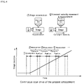
- FIG. 4 A difference from the conventional line mapping is described using Fig. 4 and 5 .
- a synchronizing operation of the movable stage 40 and the CCD detector 60 in the present embodiment is shown together with an acceleration period of the movable stage 40.
- the CCD detector 60 does not start the exposure.
- the exposure is started.
- the velocity becomes stable, it maintains the condition and performs the light detection cycle of the exposure and read-out repeatedly.
- Other operation order is not given to the movable stage 40 until the row-changing operation and the like are required, and the continuous scanning of the movable stage 40 shall not be interrupted.
- Fig. 5 the method of the conventional line mapping is shown.
- the object of the conventional line mapping is to obtain mapping data with high spatial resolution. Accordingly, the number of spectral data obtained from the mapping range of the same size as the present embodiment is extremely large.
- the direction which the linear irradiation region I S is moved is the direction orthogonal to the longitudinal direction of the linear irradiation region I S (X direction), and the row-changing operation is performed as required.
- the light detection cycle (exposure and read-out) of the CCD detector is performed while the sample is stopped.
- positioning of the sample by the movable stage has to be performed for the number of grids aligned in the X direction to align the linear irradiation region I S to the grid column which spectra are desired to be obtained. Since it takes time for the acceleration and deceleration and the setting of the stage, time for one positioning becomes longer. This time differs in accordance with the kinds of the stage.
- the light detection cycle of the exposure and read-out is started. That is, the exposure is performed while the sample is stopped, and the spectral data from the parts of the sample in accordance with the linear irradiation region I S are obtained.
- the sample is positioned again to align the linear irradiation region I S to the adjacent grid column.
- Such movements of the stage in steps are referred to as stepwise movements, and the movement and the exposure (including the read-out) is performed alternately. Further, the binning process is not used in the CCD detector, and a fine read-out for each pixel is performed.
- mapping data with high spatial resolution can be obtained by such stepwise movement of the movable stage and read-out for each pixel of the CCD detector.
- the size of the linear irradiation region I S of the sample is 1 ⁇ m in width and 100 ⁇ m in length and the number of pixels of the CCD detector is 100 ⁇ 100 like the present embodiment
- the size of one grid for the conventional line mapping is as follows. The region of linear irradiation is positioned in stepwise by 1 ⁇ m in the X direction. Then, 100 spectra are obtained in one cycle of the exposure and read-out. Therefore, one side of the grid which obtains one spectrum (spatial resolution) is 1 ⁇ m.
- the problems of the conventional line mapping is not only that the number of measurement points for obtaining spectral data are excessive, but also that it is difficult to shorten the measurement time since it takes excess time for moving the movable stage for each light detection cycle of the CCD detector. Particularly, setting time until the stage stops after a deceleration period is necessary when the movable stage is stopped, and this leads to the loss of the measurement time, too.
- Supposing that conventional line mapping is used to obtain macro mapping data for example, n x n spectral data obtained from n x n grids can be added and averaged to treat them as one spectral data. However, this does not shorten the measurement time because each spectral data are obtained from numerous measurement points.
- S/N of the CCD detector becomes the value proportional to the square root of n in the added and averaged grid (n x n), but read-out noise at each channel remains.
- the line macro mapping of the present embodiment there is no stepwise movement and the measurement time is significantly shortened since the sample is continuously scanned while exposed. Further, in the present embodiment, the number of read-out is significantly reduced since the light detection cycle of the CCD detector is performed only once for the grid of the same size as the grid (n x n) which is added and averaged in the conventional type.
- the line macro mapping of the present embodiment can be regarded as one which has sacrificed the spatial resolution, but the spatial resolution is enough for a wide range mapping measurement. Furthermore, as described above, macro mapping data can be obtained quickly by the significant shortening of the measurement time.
- S/N of the CCD detector is proportional to the exposure time T. Accordingly, it is advantageous in the point that S/N can be made higher when the exposure time is extended like in the present embodiment than the added average of the conventional line mapping.
- Fig. 6 an application example of the line macro mapping measurement of the present embodiment is shown.
- 100 grids are arranged in the X and Y directions respectively in a mapping range of 10 mm square. Each grid has one side of 100 ⁇ m.
- the number of measurement points is 10,000.
- Fig. 6 is a list showing the scanning velocity of the movable stage 40 and measurement time when the exposure time of one grid (100 ⁇ m square) is set in five ways (1, 10, 100, 500 and 1000 ms).
- the measurement time is calculated as the read-out time and row-changing time of the CCD detector 60 being zero. As the exposure time becomes longer, the measurement time becomes longer.
- the measurement times are significantly shortened from the measurement times of the conventional line mapping.
- the measurement time can be shortened for 10 seconds.
- a movable stage suitable for high speed movement of 100 mm/s will be required.
- the set lower limit of the exposure time is 10 ms. This is because it takes several ms for reading out in FVB mode.
- the spectral read-out velocity of an exemplary detector is 269 points in 1 seconds (4 ms per one point), and there are other detectors of 75 points (14 ms), 122 points (8.2 ms), and 396 points (2.5 ms).
- the line macro mapping a blank region by the CCD read-out is formed when the exposure time is shortened. On the contrary, the blank region becomes smaller when the exposure time is longer. To make S/N higher, the exposure time is desired to be as long as possible. On the other hand, when the exposure time is made longer to 1000 ms, the measurement time becomes 166 minutes. As for the macro mapping of the component distribution of a tablet, the measurement time is desired to be shorter. If the exposure time is set between 10 to 500 ms, S/N, the scanning velocity and the measurement time will be within a practical range. For example, if the exposure time is set to 100 ms, the measurement time will be 17 minutes, and an extremely practical macro mapping measurement can be achieved. It is more preferable to set the exposure time to 50 ms or more.
- the performance of the movable stage 40 is enough if it can adapt to the scanning velocity of 1 mm/s, and it is not necessary for the movable stage to adapt to high speed of 10 mm/s or more.
- Fig. 7 is a list showing measurement times of when the size of one side of the grid that are aligned in the mapping range is set in 4 ways (1, 5, 10 and 100 ⁇ m steps) in the measurement of the component distribution of a tablet like Fig. 6 .
- the number of measurement points becomes one hundred million, four million, one million and ten thousand.
- the longitudinal direction of the linear irradiation region in Fig. 6 is 100 ⁇ m
- the longitudinal direction of the linear irradiation region is set to 1, 5, 10 and 100 ⁇ m in accordance with the size of the grid in Fig. 7 .
- the measurement time becomes longer when the number of measurement points increases, but, in any measurement condition, the measurement time is significantly shortened in comparison to the measurement time of the conventional line mapping measurement. As it can be seen from the list, the measurement times are still too long in 1 ⁇ m and 5 ⁇ m steps for the macro mapping of the component distribution of a tablet. The condition of measuring one grid in 100 ⁇ m step is most practical for a mapping region of 10 mm square.
- mapping data an average spectral data based on the spectral image with high spatial resolution can be obtained although spatial resolution is deteriorated as mapping data, and mapping data of a wide range can be obtained at high speed (2) with high wavelength resolution and (3) high sensitivity.
- (1) to (3) are described in detail.
- Fig. 8 is a schematic view of a Raman spectroscope 110 which is a second embodiment of the microspectroscope of the present invention.
- the differences from the configuration of the Raman spectroscope 10 of Fig. 1 are a mapping range setting portion 172, continuous scanning control portion 174 and light detection control portion 176 in a control device 170, and other configuration are the same.
- the present embodiment is characterized in that the mapping range setting portion 172 sets a grid to a smaller size relative to the dimension of the longitudinal direction of the linear irradiation region I S and the light detection control portion 176 makes the CCD detector 60 to perform an ordinary binning process.
- one side of one grid was set to 100 ⁇ m, for example.
- the mapping range setting portion 172 sets one side of one grid to (100/n) ⁇ m.
- the grid can be set to a desired size by changing the moving velocity of the movable stage 40 and the cycle period (especially the exposure period) of the light detection.
- the upper limit of n is described.
- the value of which the dimension of the longitudinal direction of the linear irradiation region I S is divided by n becomes the width dimension of the irradiation region I S
- the value is the upper limit of n.
- the upper limit of n value is 100.
- a mapping range of 36 grids are shown, and the region with hatching is the position of the linear irradiation region I S at the start of the exposure period of each light detection cycle.
- the linear irradiation light irradiates the left end part of n grids simultaneously. This means that the moving range of the linear irradiation region I S at one light detection cycle becomes a rectangle having the dimension of the longitudinal direction of this irradiation region I S as the long side and the long side becomes n times the short side of the rectangle.
- the part of the sample on which the linear irradiation region I S is formed moves within 3 grids simultaneously, and thus the CCD detector 60 receives the spectral image of Raman light from parts of different grids during exposure period.
- the light detection control part 176 makes the CCD detector 60 to perform the read-out in an ordinary binning process.
- the ordinary binning process is a process which all light-receiving elements that are aligned in a line in the longitudinal direction (the vertical direction in the drawing) of the image of the diffused linear irradiation region are divided into n groups and the light-receiving quantity (electric charge) of light-receiving elements in each group is read out collectively. That is, the entire light-receiving surface is divided into n tracks, and n spectral data in total are read out for each track.
- N spectra are the spectra corresponding to n grids that are continuously scanned simultaneously in Fig. 8 (B) .
- n spectral data that are read out in one light detection cycle are the average spectral data within n grids that the irradiation region passes during the cycle.
- the mapping measurement method of the present embodiment is basically the same as the measurement method shown in Fig. 1 .
- the ordinary binning process is performed at the light detection cycle.
- the linear irradiation region I S scans the alignment of grids for one row, but in the present embodiment, the linear irradiation region I S scans the alignment of grids for n rows collectively as shown in Fig. 9 .
- the exposure control of the CCD detector 60 it exposes in ON period and reads out at binning of n division in OFF period.
- the size of the grid that obtains spectral data can be easily set to a desired size by changing the moving velocity of the movable stage 40 or the cycle period of the light detection. Therefore, the size of one grid is not limited to the dimension of the longitudinal direction of the linear irradiation, and a mapping range of various numbers of grids can be set even in the same linear irradiation.
- a switching unit for switching the beam shaping unit to an on-line and off-line position relative to the optical axis of the irradiation light and irradiate a laser light from the laser device without shaping it into a linear light, if necessary, so that a beam spot can be formed on the sample.
- the spot diameter of when the irradiation light having a circular cross section is focused onto the sample without passing through the beam shaping unit is the focusing limit
- the shape of the linear irradiation light I S that is formed on the sample via the beam shaping unit has a width dimension corresponding to the focusing limit and a length dimension of 2 to 500 times the width dimension.
- the maximum settable width of the linear irradiation depends on the size of the CCD detector.
- the numbers of pixels of exemplary CCD detectors are 200, 255, 400 and 512 channels, and, taking this into consideration, the length dimension of the linear irradiation region I S is set from 2 times to 500 times of the width dimension.
- the present invention is not limited to Raman spectroscopes and is applied to fluorescence spectroscopes and infrared spectroscopes.
- a laser light is used as the irradiation light in the present embodiment, but an infrared light from high luminance ceramic light source or a halogen lamp are used as the irradiation light in infrared spectroscopes.
- the present invention is not limited to Raman spectral measurement, and is applied to measurement devices for spectra such as light emissions by a reflected light, a transmitted light and an excitation light of the irradiation light to the sample.
- the comparative example of Fig. 10 (A) is a "point mapping method". All area of the mapping range is scanned by a beam spot. Although existing linear stages, EMCCD detectors and multivariate analysis are applied for acceleration, there is a limit for acceleration since there are excessive measurement points, and the exposure time for one point has to be shortened. For detection of a weak light such as Raman light, shortening of the exposure time needs to be avoided due to problems of S/N. For these reasons, the point mapping is not suitable for a wide range mapping.
- the comparative example of Fig. 10 (B) is a "conventional line mapping method". Compared to the point mapping, it can be said that spectral data from a plurality of parts along the longitudinal direction of the linear irradiation can be obtained collectively by one cycle of light detection of the CCD detector. However, similar to the description using Fig. 5 , the measurement time cannot be sufficiently shortened for the application to a wide range mapping.
- a high magnification objective lens can be adopted in the same way as the conventional line mapping measurement.
- the reason why the low magnification objective lens is not preferable is described.
- the number of measurement points can be reduced if the beam spot on the sample is bigger, and thus the measurement time can be shortened.
- the beam spot can be made bigger since NA of the lens is small.
- a problem of detection sensitivity (throughput) of the objective lens occurs.
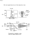
- the hatching in Fig. 11 (A) shows the capturing range by a low NA lens. As shown, when the low magnification lens having small NA is adopted, the detection sensitivity of the objective lens will be deteriorated.
- Fig. 11 (B) when the diameter dimension of the incident parallel light to this objective lens is 3.3 mm, substantial NA is derived as shown below.
- ⁇ is the wavelength (0.532 ⁇ m) of the incident laser light.
- an energy loss when the F value of the spectrometer having a focal distance of 20 cm is 8 is investigated.
- the focal distance f2 of the imaging lens is 85 mm
- the spectrometer can receive the parallel light flux up to 10.6 mm. Energy loss occurs due to the relationship between this and the pupil diameter (11.5 mm) of the objective lens.
- the beam size at the slit position in Fig. 11 (B) is derived as shown below from the relationship to an image magnification M.
- the comparative example of Fig. 10 (C) and (D) is a "macro irradiation method" and "pseudo-backward irradiation method".
- a method to make the beam spot bigger by using high NA objective lens there are methods of lowering the substantial NA of the incident side as shown in Fig. 10 (C), destroying the parallel light of the incident side, or pseudo-back scattering like Fig. 10 (D).
- the image size at the incident slit of the spectrometer is derived as follows.
- the width of the incident slit needs to be made wider.
- an imaging state at the slit width and the CCD detector when the beam spot diameter on the sample is 1 ⁇ m is shown.
- the spectra obtained in this comparative example have weak peaks and are broad.
- the wavelength resolution in the CCD detector is deteriorated.
- high NA objective lens it does not make the beam spot on the sample big, but it forms a linear shaped irradiation region by the linear irradiation.
- the slit width does not need to be widened, and a measurement with high wavelength resolution is possible.
- the irradiation area of the irradiation beam is made bigger by oblique incidence.
- wavelength resolution is deteriorated due to the irradiation area being big.
- the operation distance between the lens and the sample will be smaller when high NA lens is used as the objective lens, and thus oblique incidence will not be possible.
- the comparative example of Fig. 10 (E) is a method which uses a "low magnification dedicated optical system".
- a low magnification dedicated optical system There is a problem of deterioration of the detection sensitivity due to the small NA when a low magnification objective lens is used.
- the microspectroscope of the present invention is advantageous from the point of wavelength resolution and detection sensitivity, is suitable for high speed mapping measurement, and also is suitable for switching the magnification of the objective lens.
- measurement points refer to a region having a specific area that is a subject for obtaining spectra.
- squares and rectangles include not only squares and rectangles in a strict meaning but also shapes having rounded angles. Particularly, when the shape of the moving range of the linear beam is a rectangle, a shape which the short side of the rectangle is circular is included.
Landscapes
- Physics & Mathematics (AREA)
- Spectroscopy & Molecular Physics (AREA)
- General Physics & Mathematics (AREA)
- Chemical & Material Sciences (AREA)
- Analytical Chemistry (AREA)
- Health & Medical Sciences (AREA)
- Optics & Photonics (AREA)
- Nuclear Medicine, Radiotherapy & Molecular Imaging (AREA)
- Life Sciences & Earth Sciences (AREA)
- Biochemistry (AREA)
- General Health & Medical Sciences (AREA)
- Immunology (AREA)
- Pathology (AREA)
- Investigating, Analyzing Materials By Fluorescence Or Luminescence (AREA)
- Investigating Or Analysing Materials By Optical Means (AREA)
Claims (6)
- Ein Mikrospektroskop für eine zwei- oder dreidimensionale Abbildungsmessung, umfassend:eine Strahlformungseinheit (26) zur Formung eines Bestrahlungslichts in eine lineare Form;einen beweglichen Tisch (40) zur Positionierung einer Probe in einer Fokussierungsposition des linear geformten Bestrahlungslichts;eine Fokussierlinse (32) zum Fokussieren von Licht aus einem auf der Probe gebildeten linearen Bestrahlungsbereich;einen Schlitz (38), der an einer Abbildungsposition des durch die Fokussierlinse (32) gebildeten linearen Bestrahlungsbereichs vorgesehen ist und parallel zur Längsrichtung eines Bildes des linearen Bestrahlungsbereichs liegt;eine spektroskopische Einheit (50) zum Empfangen des durch den Spalt (38) einfallenden Lichts und zum Dispergieren des Bildes des linearen Bestrahlungsbereichs in einer Richtung orthogonal zur Längsrichtung des Bildes;eine Lichterfassungseinheit (60) zum Erfassen des gestreuten Bildes des linearen Bestrahlungsbereichs; undeine Abbildungsmessungssteuereinheit (70) zum Durchführen der Abbildungsmessung durch Synchronisieren des beweglichen Tisches (40) und der Lichterfassungseinheit (60), wobeidie Lichterfassungseinheit (60) aus einer Lichtempfangselementgruppe besteht, die in zwei Richtungen, der Längsrichtung des Bildes des linearen Bestrahlungsbereichs und einer dazu orthogonalen Streurichtung, angeordnet ist, dadurch gekennzeichnet, dassdie Steuereinheit für die Abbildungsmessung (70) umfasst:einen Steuerabschnitt (74) für kontinuierliche Abtastung zum kontinuierlichen Bewegen des linearen Bestrahlungsbereichs in einer Richtung orthogonal zur Längsrichtung des linearen Bestrahlungsbereichs durch die Bewegung des beweglichen Tisches (40) ohne Anhalten in der Probe;einen Lichterfassungs-Steuerabschnitt (76), um die Lichterfassungseinheit (60) zu veranlassen, einen Lichterfassungszyklus durchzuführen, der aus einer Belichtungsperiode und einer Ausleseperiode der Lichterfassungseinheit (60) während der kontinuierlichen Bewegung des linearen Bestrahlungsbereichs besteht, und um ein Durchschnittsspektrum eines Bewegungsbereichs des linearen Bestrahlungsbereichs während eines Lichterfassungszyklus zu erhalten; undeinen Konfigurationsabschnitt (78) für Abbildungsdaten zum Speichern des durchschnittlichen Spektrums für jeden Lichterfassungszyklus und zum Konfigurieren von Abbildungsdaten;wobei der Lichterfassungs-Steuerabschnitt (76) ferner so konfiguriert ist, dass er ein Spektralbild als ein Durchschnittsspektrum durch einen vollständigen Binning-Prozess erfasst; unddas Mikrospektroskop ist ferner so konfiguriert, dass es eine Belichtung während des Lichterfassungszyklus einleitet, sobald die Bewegungsgeschwindigkeit des beweglichen Tisches (40) stabil wird.
- Mikrospektroskop nach Anspruch 1, wobei die Abbildungsmessungs-Steuereinheit (70) so konfiguriert ist, dass sie die Bewegungsgeschwindigkeit des beweglichen Tisches (40) oder die Zyklusdauer des Lichterfassungszyklus so ändert, dass der Bewegungsbereich während eines Lichterfassungszyklus einem Quadrat entspricht, das eine Dimension der Längsrichtung des linearen Bestrahlungsbereichs als eine Seite hat.
- Mikrospektroskop nach Anspruch 2, wobei der Lichterfassungs-Steuerabschnitt (76) so konfiguriert ist, dass er einen Prozess zum kollektiven Auslesen aller Lichtempfangselemente durchführt, die in der Ausleseperiode in einer Linie in der Längsrichtung des gestreuten Bildes des linearen Bestrahlungsbereichs ausgerichtet sind.
- Mikrospektroskop nach Anspruch 1, wobei die Abbildungsmessungs-Steuereinheit (78) so konfiguriert ist, dass sie die Bewegungsgeschwindigkeit des beweglichen Tisches (40) oder die Zyklusdauer des Lichterfassungszyklus unter Verwendung von Impulssignalen so ändert, dass der Bewegungsbereich während eines Lichterfassungszyklus einem Rechteck entspricht, das eine Abmessung in der Längsrichtung des linearen Bestrahlungsbereichs als lange Seite hat, und die lange Seite dem n-fachen der kurzen Seite des Rechtecks entspricht, wobei n eine ganze Zahl von zwei oder mehr ist.
- Mikrospektroskop nach Anspruch 4, wobei der Lichterfassungs-Steuerabschnitt (76) so konfiguriert ist, dass er alle Lichtempfangselemente, die in einer Linie in der Längsrichtung des gestreuten Bildes des linearen Bestrahlungsbereichs ausgerichtet sind, in n Gruppen unterteilt und den Prozess des kollektiven Auslesens der Lichtempfangselemente jeder Gruppe in der Ausleseperiode durchführt.
- Mikrospektroskop nach einem der Ansprüche 1 bis 5, umfassend:
eine Schalteinheit zum Umschalten der Strahlformungseinheit (26) in eine Online- und Offline-Position relativ zu einer optischen Achse des Bestrahlungslichts,
wobei,
wenn ein Punktdurchmesser, bei dem das Bestrahlungslicht mit einem kreisförmigen Querschnitt auf die Probe fokussiert wird, ohne die Strahlformungseinheit (26) zu passieren, als Fokussierungsgrenze betrachtet wird, die Form eines linearen Bestrahlungsbereichs, der auf der Probe durch die Strahlformungseinheit (26) gebildet wird, eine Breitenabmessung hat, die der Fokussierungsgrenze entspricht, und eine Längenabmessung, die das 2 bis 500-fache der Breitenabmessung beträgt.
Applications Claiming Priority (2)
| Application Number | Priority Date | Filing Date | Title |
|---|---|---|---|
| JP2015062307A JP5901814B1 (ja) | 2015-03-25 | 2015-03-25 | 顕微分光装置 |
| PCT/JP2016/058889 WO2016152823A1 (ja) | 2015-03-25 | 2016-03-22 | 顕微分光装置 |
Publications (3)
| Publication Number | Publication Date |
|---|---|
| EP3276336A1 EP3276336A1 (de) | 2018-01-31 |
| EP3276336A4 EP3276336A4 (de) | 2018-12-26 |
| EP3276336B1 true EP3276336B1 (de) | 2022-12-07 |
Family
ID=55747687
Family Applications (1)
| Application Number | Title | Priority Date | Filing Date |
|---|---|---|---|
| EP16768726.8A Active EP3276336B1 (de) | 2015-03-25 | 2016-03-22 | Mikrospektroskop |
Country Status (4)
| Country | Link |
|---|---|
| US (1) | US10295470B2 (de) |
| EP (1) | EP3276336B1 (de) |
| JP (1) | JP5901814B1 (de) |
| WO (1) | WO2016152823A1 (de) |
Families Citing this family (17)
| Publication number | Priority date | Publication date | Assignee | Title |
|---|---|---|---|---|
| JP6583442B2 (ja) * | 2016-02-19 | 2019-10-02 | 株式会社ニコン | 試料作製方法および試料作製装置 |
| CN111142251B (zh) | 2016-10-26 | 2022-03-25 | 合肥百会拓知科技有限公司 | 一种具有三维成像能力的显微镜和成像方法 |
| CN106525240B (zh) * | 2016-12-29 | 2019-03-19 | 同方威视技术股份有限公司 | 光谱探测装置 |
| EP3372966B1 (de) * | 2017-03-10 | 2021-09-01 | Hitachi High-Tech Analytical Science Limited | Tragbarer analysator zur optischen emissionsspektroskopie |
| CN110678722A (zh) * | 2017-06-01 | 2020-01-10 | 柯尼卡美能达株式会社 | 分光光度计 |
| CN109507166A (zh) * | 2017-09-15 | 2019-03-22 | Ravr有限公司 | 一种双通道微型拉曼光谱仪 |
| IL280200B2 (en) * | 2018-07-25 | 2024-02-01 | Nova Ltd | Optical technique for material characterization |
| GB2572662B (en) * | 2018-10-05 | 2020-06-03 | Res & Innovation Uk | Raman spectrometer |
| AU2020281945B2 (en) * | 2019-05-31 | 2025-06-05 | Cytognos, S.L. | Hyperspectral quantitative imaging cytometry system |
| JP6788298B1 (ja) * | 2019-12-17 | 2020-11-25 | 日本分光株式会社 | 蛍光観察機能を備えるラマン顕微装置 |
| JP7412758B2 (ja) * | 2020-04-15 | 2024-01-15 | 日本分光株式会社 | 顕微分光測定装置 |
| CN113514447B (zh) * | 2021-07-14 | 2022-08-12 | 清华大学 | 一种基于sers的体液检测方法及系统 |
| JPWO2023228449A1 (de) | 2022-05-27 | 2023-11-30 | ||
| KR20250016064A (ko) | 2022-05-27 | 2025-02-03 | 하마마츠 포토닉스 가부시키가이샤 | 분광 장치, 라만 분광 측정 장치 및 분광 방법 |
| US20250341469A1 (en) | 2022-05-27 | 2025-11-06 | Hamamatsu Photonics K.K. | Spectroscopic device, raman spectroscopic measurement device, and spectroscopic method |
| CN116718578B (zh) * | 2023-08-11 | 2023-10-27 | 深圳赛陆医疗科技有限公司 | 超分辨显微成像系统和成像方法 |
| CN117491327B (zh) * | 2023-11-06 | 2024-12-06 | 山西大学 | 一种显微共聚焦荧光光谱仪 |
Citations (1)
| Publication number | Priority date | Publication date | Assignee | Title |
|---|---|---|---|---|
| US20140313313A1 (en) * | 2000-05-03 | 2014-10-23 | Leica Biosystems Imaging, Inc. | Fully automatic rapid microscope slide scanner |
Family Cites Families (14)
| Publication number | Priority date | Publication date | Assignee | Title |
|---|---|---|---|---|
| JP3667397B2 (ja) | 1995-09-04 | 2005-07-06 | 日本分光株式会社 | ラマン分光装置 |
| EP3564851B1 (de) | 2004-09-01 | 2022-12-07 | Leica Biosystems Imaging Inc. | System und verfahren zur datenverwaltung in einem linearen array-basierten mikroskop-objektträgerscanner |
| JP4887989B2 (ja) | 2005-12-02 | 2012-02-29 | ナノフォトン株式会社 | 光学顕微鏡及びスペクトル測定方法 |
| GB0803798D0 (en) * | 2008-02-29 | 2008-04-09 | Renishaw Plc | Spectroscopic apparatus and methods |
| US8761486B2 (en) * | 2011-02-22 | 2014-06-24 | Bio-Rad Laboratories, Inc. | Line scan cytometry systems and methods |
| JP5838466B2 (ja) | 2011-03-11 | 2016-01-06 | ナノフォトン株式会社 | 光学顕微鏡、及び分光測定方法 |
| EP2694932B1 (de) * | 2011-04-07 | 2018-02-21 | The UWM Research Foundation, Inc | Hochgeschwindigkeitsmikroskop mit spektraler auflösung |
| DE102011007751B4 (de) * | 2011-04-20 | 2023-10-19 | Carl Zeiss Microscopy Gmbh | Weitfeldmikroskop und Verfahren zur Weitfeldmikroskopie |
| JP5989109B2 (ja) * | 2011-07-13 | 2016-09-07 | ライカ バイオシステムズ イメージング インコーポレイテッド | 蛍光顕微鏡システムの標準化 |
| JP5846844B2 (ja) * | 2011-10-14 | 2016-01-20 | 株式会社キーエンス | 拡大観察装置 |
| US9924105B2 (en) * | 2011-12-12 | 2018-03-20 | Visys Nv | System and method for individually inspecting objects in a stream of products and a sorting apparatus comprising such system |
| JP5973846B2 (ja) * | 2012-08-30 | 2016-08-23 | 東レエンジニアリング株式会社 | 撥液性樹脂の改質パターン検査方法および装置 |
| WO2014134172A1 (en) * | 2013-02-26 | 2014-09-04 | Cornell University | Event correlation using data having different time resolutions |
| US8982238B2 (en) * | 2013-07-02 | 2015-03-17 | Omnivision Technologies, Inc. | Multi-target automatic exposure and gain control based on pixel intensity distribution |
-
2015
- 2015-03-25 JP JP2015062307A patent/JP5901814B1/ja active Active
-
2016
- 2016-03-22 EP EP16768726.8A patent/EP3276336B1/de active Active
- 2016-03-22 US US15/560,256 patent/US10295470B2/en active Active
- 2016-03-22 WO PCT/JP2016/058889 patent/WO2016152823A1/ja not_active Ceased
Patent Citations (1)
| Publication number | Priority date | Publication date | Assignee | Title |
|---|---|---|---|---|
| US20140313313A1 (en) * | 2000-05-03 | 2014-10-23 | Leica Biosystems Imaging, Inc. | Fully automatic rapid microscope slide scanner |
Also Published As
| Publication number | Publication date |
|---|---|
| US20180067053A1 (en) | 2018-03-08 |
| WO2016152823A1 (ja) | 2016-09-29 |
| JP2016180732A (ja) | 2016-10-13 |
| EP3276336A1 (de) | 2018-01-31 |
| EP3276336A4 (de) | 2018-12-26 |
| US10295470B2 (en) | 2019-05-21 |
| JP5901814B1 (ja) | 2016-04-13 |
Similar Documents
| Publication | Publication Date | Title |
|---|---|---|
| US10295470B2 (en) | Microspectroscope | |
| JP5712342B2 (ja) | 光学顕微鏡、及びスペクトル測定方法 | |
| JP4887989B2 (ja) | 光学顕微鏡及びスペクトル測定方法 | |
| JP5905140B1 (ja) | 顕微分光装置 | |
| JP6091100B2 (ja) | 共焦点顕微装置 | |
| CN105556370B (zh) | 高分辨率扫描显微术 | |
| US9671600B2 (en) | Light microscope and microscopy method | |
| US9435741B2 (en) | Spectrometry device and spectrometry method | |
| US12146832B2 (en) | Microscope and method of microscopy for providing illumination light and generating an illumination pattern | |
| TW201800718A (zh) | 用於諸如晶圓之物件之2d/3d檢測的彩色共焦裝置及方法 | |
| US7724363B2 (en) | Device for multifocal confocal microscopic determination of spatial distribution and for multifocal fluctuation analysis of fluorescent molecules and structures with flexible spectral detection | |
| US10371932B2 (en) | Light field imaging with scanning optical unit | |
| TW201802432A (zh) | 用於諸如晶圓之物件之2d/3d檢測之具有可變空間解析度的彩色共焦裝置及方法 | |
| EP2243008B1 (de) | Gerät mit einem linienscanner für die raman spektroskopie | |
| WO2012124303A1 (ja) | 光学顕微鏡、及び分光測定方法 | |
| JP2010054391A (ja) | 光学顕微鏡、及びカラー画像の表示方法 | |
| JP2017529529A (ja) | 分光装置 | |
| CN114442298A (zh) | 用于捕获图像数据的设备和方法 | |
| JP7830922B2 (ja) | ラマン顕微鏡 | |
| EP2828700A1 (de) | Mehrfarbiges konfokales mikroskop und bildgebungsverfahren | |
| JP5415854B2 (ja) | 分光装置および走査型顕微鏡装置 | |
| US12601901B2 (en) | Detection device for a laser scanning microscope | |
| JP2007506146A (ja) | 共焦点レーザ走査顕微鏡 | |
| JP2006125970A (ja) | 分光装置および分光システム | |
| JP5190603B2 (ja) | 光学顕微鏡、及び観察方法 |
Legal Events
| Date | Code | Title | Description |
|---|---|---|---|
| STAA | Information on the status of an ep patent application or granted ep patent |
Free format text: STATUS: THE INTERNATIONAL PUBLICATION HAS BEEN MADE |
|
| PUAI | Public reference made under article 153(3) epc to a published international application that has entered the european phase |
Free format text: ORIGINAL CODE: 0009012 |
|
| STAA | Information on the status of an ep patent application or granted ep patent |
Free format text: STATUS: REQUEST FOR EXAMINATION WAS MADE |
|
| 17P | Request for examination filed |
Effective date: 20170921 |
|
| AK | Designated contracting states |
Kind code of ref document: A1 Designated state(s): AL AT BE BG CH CY CZ DE DK EE ES FI FR GB GR HR HU IE IS IT LI LT LU LV MC MK MT NL NO PL PT RO RS SE SI SK SM TR |
|
| AX | Request for extension of the european patent |
Extension state: BA ME |
|
| DAV | Request for validation of the european patent (deleted) | ||
| DAX | Request for extension of the european patent (deleted) | ||
| A4 | Supplementary search report drawn up and despatched |
Effective date: 20181126 |
|
| RIC1 | Information provided on ipc code assigned before grant |
Ipc: G01N 21/59 20060101ALI20181120BHEP Ipc: G01J 3/08 20060101ALI20181120BHEP Ipc: G02B 21/00 20060101ALI20181120BHEP Ipc: G01N 21/64 20060101ALI20181120BHEP Ipc: G01N 21/65 20060101ALI20181120BHEP Ipc: G01J 3/28 20060101AFI20181120BHEP Ipc: G01J 3/44 20060101ALI20181120BHEP Ipc: G01J 3/06 20060101ALI20181120BHEP Ipc: G01J 3/10 20060101ALI20181120BHEP Ipc: G01J 3/02 20060101ALI20181120BHEP |
|
| REG | Reference to a national code |
Ref country code: DE Ref legal event code: R079 Ref document number: 602016076775 Country of ref document: DE Free format text: PREVIOUS MAIN CLASS: G01N0021650000 Ipc: G01J0003280000 |
|
| RIC1 | Information provided on ipc code assigned before grant |
Ipc: G02B 21/00 20060101ALI20190625BHEP Ipc: G01N 21/64 20060101ALI20190625BHEP Ipc: G01N 21/59 20060101ALI20190625BHEP Ipc: G01J 3/10 20060101ALI20190625BHEP Ipc: G01J 3/44 20060101ALI20190625BHEP Ipc: G01J 3/08 20060101ALI20190625BHEP Ipc: G01J 3/28 20060101AFI20190625BHEP Ipc: G01N 21/65 20060101ALI20190625BHEP Ipc: G01J 3/02 20060101ALI20190625BHEP Ipc: G01J 3/06 20060101ALI20190625BHEP |
|
| GRAP | Despatch of communication of intention to grant a patent |
Free format text: ORIGINAL CODE: EPIDOSNIGR1 |
|
| STAA | Information on the status of an ep patent application or granted ep patent |
Free format text: STATUS: GRANT OF PATENT IS INTENDED |
|
| INTG | Intention to grant announced |
Effective date: 20220722 |
|
| GRAS | Grant fee paid |
Free format text: ORIGINAL CODE: EPIDOSNIGR3 |
|
| GRAA | (expected) grant |
Free format text: ORIGINAL CODE: 0009210 |
|
| STAA | Information on the status of an ep patent application or granted ep patent |
Free format text: STATUS: THE PATENT HAS BEEN GRANTED |
|
| AK | Designated contracting states |
Kind code of ref document: B1 Designated state(s): AL AT BE BG CH CY CZ DE DK EE ES FI FR GB GR HR HU IE IS IT LI LT LU LV MC MK MT NL NO PL PT RO RS SE SI SK SM TR |
|
| REG | Reference to a national code |
Ref country code: GB Ref legal event code: FG4D |
|
| REG | Reference to a national code |
Ref country code: CH Ref legal event code: EP Ref country code: AT Ref legal event code: REF Ref document number: 1536568 Country of ref document: AT Kind code of ref document: T Effective date: 20221215 |
|
| REG | Reference to a national code |
Ref country code: DE Ref legal event code: R096 Ref document number: 602016076775 Country of ref document: DE |
|
| REG | Reference to a national code |
Ref country code: IE Ref legal event code: FG4D |
|
| REG | Reference to a national code |
Ref country code: LT Ref legal event code: MG9D |
|
| REG | Reference to a national code |
Ref country code: NL Ref legal event code: MP Effective date: 20221207 |
|
| PG25 | Lapsed in a contracting state [announced via postgrant information from national office to epo] |
Ref country code: SE Free format text: LAPSE BECAUSE OF FAILURE TO SUBMIT A TRANSLATION OF THE DESCRIPTION OR TO PAY THE FEE WITHIN THE PRESCRIBED TIME-LIMIT Effective date: 20221207 Ref country code: NO Free format text: LAPSE BECAUSE OF FAILURE TO SUBMIT A TRANSLATION OF THE DESCRIPTION OR TO PAY THE FEE WITHIN THE PRESCRIBED TIME-LIMIT Effective date: 20230307 Ref country code: LT Free format text: LAPSE BECAUSE OF FAILURE TO SUBMIT A TRANSLATION OF THE DESCRIPTION OR TO PAY THE FEE WITHIN THE PRESCRIBED TIME-LIMIT Effective date: 20221207 Ref country code: FI Free format text: LAPSE BECAUSE OF FAILURE TO SUBMIT A TRANSLATION OF THE DESCRIPTION OR TO PAY THE FEE WITHIN THE PRESCRIBED TIME-LIMIT Effective date: 20221207 Ref country code: ES Free format text: LAPSE BECAUSE OF FAILURE TO SUBMIT A TRANSLATION OF THE DESCRIPTION OR TO PAY THE FEE WITHIN THE PRESCRIBED TIME-LIMIT Effective date: 20221207 |
|
| REG | Reference to a national code |
Ref country code: AT Ref legal event code: MK05 Ref document number: 1536568 Country of ref document: AT Kind code of ref document: T Effective date: 20221207 |
|
| PG25 | Lapsed in a contracting state [announced via postgrant information from national office to epo] |
Ref country code: RS Free format text: LAPSE BECAUSE OF FAILURE TO SUBMIT A TRANSLATION OF THE DESCRIPTION OR TO PAY THE FEE WITHIN THE PRESCRIBED TIME-LIMIT Effective date: 20221207 Ref country code: PL Free format text: LAPSE BECAUSE OF FAILURE TO SUBMIT A TRANSLATION OF THE DESCRIPTION OR TO PAY THE FEE WITHIN THE PRESCRIBED TIME-LIMIT Effective date: 20221207 Ref country code: LV Free format text: LAPSE BECAUSE OF FAILURE TO SUBMIT A TRANSLATION OF THE DESCRIPTION OR TO PAY THE FEE WITHIN THE PRESCRIBED TIME-LIMIT Effective date: 20221207 Ref country code: HR Free format text: LAPSE BECAUSE OF FAILURE TO SUBMIT A TRANSLATION OF THE DESCRIPTION OR TO PAY THE FEE WITHIN THE PRESCRIBED TIME-LIMIT Effective date: 20221207 Ref country code: GR Free format text: LAPSE BECAUSE OF FAILURE TO SUBMIT A TRANSLATION OF THE DESCRIPTION OR TO PAY THE FEE WITHIN THE PRESCRIBED TIME-LIMIT Effective date: 20230308 |
|
| PG25 | Lapsed in a contracting state [announced via postgrant information from national office to epo] |
Ref country code: NL Free format text: LAPSE BECAUSE OF FAILURE TO SUBMIT A TRANSLATION OF THE DESCRIPTION OR TO PAY THE FEE WITHIN THE PRESCRIBED TIME-LIMIT Effective date: 20221207 |
|
| PG25 | Lapsed in a contracting state [announced via postgrant information from national office to epo] |
Ref country code: SM Free format text: LAPSE BECAUSE OF FAILURE TO SUBMIT A TRANSLATION OF THE DESCRIPTION OR TO PAY THE FEE WITHIN THE PRESCRIBED TIME-LIMIT Effective date: 20221207 Ref country code: RO Free format text: LAPSE BECAUSE OF FAILURE TO SUBMIT A TRANSLATION OF THE DESCRIPTION OR TO PAY THE FEE WITHIN THE PRESCRIBED TIME-LIMIT Effective date: 20221207 Ref country code: PT Free format text: LAPSE BECAUSE OF FAILURE TO SUBMIT A TRANSLATION OF THE DESCRIPTION OR TO PAY THE FEE WITHIN THE PRESCRIBED TIME-LIMIT Effective date: 20230410 Ref country code: EE Free format text: LAPSE BECAUSE OF FAILURE TO SUBMIT A TRANSLATION OF THE DESCRIPTION OR TO PAY THE FEE WITHIN THE PRESCRIBED TIME-LIMIT Effective date: 20221207 Ref country code: CZ Free format text: LAPSE BECAUSE OF FAILURE TO SUBMIT A TRANSLATION OF THE DESCRIPTION OR TO PAY THE FEE WITHIN THE PRESCRIBED TIME-LIMIT Effective date: 20221207 Ref country code: AT Free format text: LAPSE BECAUSE OF FAILURE TO SUBMIT A TRANSLATION OF THE DESCRIPTION OR TO PAY THE FEE WITHIN THE PRESCRIBED TIME-LIMIT Effective date: 20221207 |
|
| PG25 | Lapsed in a contracting state [announced via postgrant information from national office to epo] |
Ref country code: SK Free format text: LAPSE BECAUSE OF FAILURE TO SUBMIT A TRANSLATION OF THE DESCRIPTION OR TO PAY THE FEE WITHIN THE PRESCRIBED TIME-LIMIT Effective date: 20221207 Ref country code: IS Free format text: LAPSE BECAUSE OF FAILURE TO SUBMIT A TRANSLATION OF THE DESCRIPTION OR TO PAY THE FEE WITHIN THE PRESCRIBED TIME-LIMIT Effective date: 20230407 Ref country code: AL Free format text: LAPSE BECAUSE OF FAILURE TO SUBMIT A TRANSLATION OF THE DESCRIPTION OR TO PAY THE FEE WITHIN THE PRESCRIBED TIME-LIMIT Effective date: 20221207 |
|
| REG | Reference to a national code |
Ref country code: DE Ref legal event code: R097 Ref document number: 602016076775 Country of ref document: DE |
|
| PLBE | No opposition filed within time limit |
Free format text: ORIGINAL CODE: 0009261 |
|
| STAA | Information on the status of an ep patent application or granted ep patent |
Free format text: STATUS: NO OPPOSITION FILED WITHIN TIME LIMIT |
|
| PG25 | Lapsed in a contracting state [announced via postgrant information from national office to epo] |
Ref country code: MC Free format text: LAPSE BECAUSE OF FAILURE TO SUBMIT A TRANSLATION OF THE DESCRIPTION OR TO PAY THE FEE WITHIN THE PRESCRIBED TIME-LIMIT Effective date: 20221207 Ref country code: DK Free format text: LAPSE BECAUSE OF FAILURE TO SUBMIT A TRANSLATION OF THE DESCRIPTION OR TO PAY THE FEE WITHIN THE PRESCRIBED TIME-LIMIT Effective date: 20221207 |
|
| REG | Reference to a national code |
Ref country code: CH Ref legal event code: PL |
|
| 26N | No opposition filed |
Effective date: 20230908 |
|
| PG25 | Lapsed in a contracting state [announced via postgrant information from national office to epo] |
Ref country code: SI Free format text: LAPSE BECAUSE OF FAILURE TO SUBMIT A TRANSLATION OF THE DESCRIPTION OR TO PAY THE FEE WITHIN THE PRESCRIBED TIME-LIMIT Effective date: 20221207 |
|
| REG | Reference to a national code |
Ref country code: BE Ref legal event code: MM Effective date: 20230331 |
|
| PG25 | Lapsed in a contracting state [announced via postgrant information from national office to epo] |
Ref country code: LU Free format text: LAPSE BECAUSE OF NON-PAYMENT OF DUE FEES Effective date: 20230322 |
|
| REG | Reference to a national code |
Ref country code: IE Ref legal event code: MM4A |
|
| PG25 | Lapsed in a contracting state [announced via postgrant information from national office to epo] |
Ref country code: LI Free format text: LAPSE BECAUSE OF NON-PAYMENT OF DUE FEES Effective date: 20230331 Ref country code: IE Free format text: LAPSE BECAUSE OF NON-PAYMENT OF DUE FEES Effective date: 20230322 Ref country code: CH Free format text: LAPSE BECAUSE OF NON-PAYMENT OF DUE FEES Effective date: 20230331 |
|
| PG25 | Lapsed in a contracting state [announced via postgrant information from national office to epo] |
Ref country code: BE Free format text: LAPSE BECAUSE OF NON-PAYMENT OF DUE FEES Effective date: 20230331 |
|
| PG25 | Lapsed in a contracting state [announced via postgrant information from national office to epo] |
Ref country code: IT Free format text: LAPSE BECAUSE OF FAILURE TO SUBMIT A TRANSLATION OF THE DESCRIPTION OR TO PAY THE FEE WITHIN THE PRESCRIBED TIME-LIMIT Effective date: 20221207 |
|
| PG25 | Lapsed in a contracting state [announced via postgrant information from national office to epo] |
Ref country code: BG Free format text: LAPSE BECAUSE OF FAILURE TO SUBMIT A TRANSLATION OF THE DESCRIPTION OR TO PAY THE FEE WITHIN THE PRESCRIBED TIME-LIMIT Effective date: 20221207 |
|
| PG25 | Lapsed in a contracting state [announced via postgrant information from national office to epo] |
Ref country code: BG Free format text: LAPSE BECAUSE OF FAILURE TO SUBMIT A TRANSLATION OF THE DESCRIPTION OR TO PAY THE FEE WITHIN THE PRESCRIBED TIME-LIMIT Effective date: 20221207 |
|
| PG25 | Lapsed in a contracting state [announced via postgrant information from national office to epo] |
Ref country code: CY Free format text: LAPSE BECAUSE OF FAILURE TO SUBMIT A TRANSLATION OF THE DESCRIPTION OR TO PAY THE FEE WITHIN THE PRESCRIBED TIME-LIMIT; INVALID AB INITIO Effective date: 20160322 |
|
| PG25 | Lapsed in a contracting state [announced via postgrant information from national office to epo] |
Ref country code: HU Free format text: LAPSE BECAUSE OF FAILURE TO SUBMIT A TRANSLATION OF THE DESCRIPTION OR TO PAY THE FEE WITHIN THE PRESCRIBED TIME-LIMIT; INVALID AB INITIO Effective date: 20160322 |
|
| PG25 | Lapsed in a contracting state [announced via postgrant information from national office to epo] |
Ref country code: TR Free format text: LAPSE BECAUSE OF FAILURE TO SUBMIT A TRANSLATION OF THE DESCRIPTION OR TO PAY THE FEE WITHIN THE PRESCRIBED TIME-LIMIT Effective date: 20221207 |
|
| PGFP | Annual fee paid to national office [announced via postgrant information from national office to epo] |
Ref country code: GB Payment date: 20260324 Year of fee payment: 11 |
|
| PGFP | Annual fee paid to national office [announced via postgrant information from national office to epo] |
Ref country code: DE Payment date: 20260319 Year of fee payment: 11 |
|
| PGFP | Annual fee paid to national office [announced via postgrant information from national office to epo] |
Ref country code: FR Payment date: 20260320 Year of fee payment: 11 |