EP3255677A1 - Verfahren zur herstellung einer finfet-vorrichtung - Google Patents
Verfahren zur herstellung einer finfet-vorrichtung Download PDFInfo
- Publication number
- EP3255677A1 EP3255677A1 EP17173739.8A EP17173739A EP3255677A1 EP 3255677 A1 EP3255677 A1 EP 3255677A1 EP 17173739 A EP17173739 A EP 17173739A EP 3255677 A1 EP3255677 A1 EP 3255677A1
- Authority
- EP
- European Patent Office
- Prior art keywords
- gate
- contact
- insulator layer
- insulator
- layer
- Prior art date
- Legal status (The legal status is an assumption and is not a legal conclusion. Google has not performed a legal analysis and makes no representation as to the accuracy of the status listed.)
- Withdrawn
Links
Images





Classifications
-
- H—ELECTRICITY
- H10—SEMICONDUCTOR DEVICES; ELECTRIC SOLID-STATE DEVICES NOT OTHERWISE PROVIDED FOR
- H10D—INORGANIC ELECTRIC SEMICONDUCTOR DEVICES
- H10D84/00—Integrated devices formed in or on semiconductor substrates that comprise only semiconducting layers, e.g. on Si wafers or on GaAs-on-Si wafers
- H10D84/80—Integrated devices formed in or on semiconductor substrates that comprise only semiconducting layers, e.g. on Si wafers or on GaAs-on-Si wafers characterised by the integration of at least one component covered by groups H10D12/00 or H10D30/00, e.g. integration of IGFETs
- H10D84/82—Integrated devices formed in or on semiconductor substrates that comprise only semiconducting layers, e.g. on Si wafers or on GaAs-on-Si wafers characterised by the integration of at least one component covered by groups H10D12/00 or H10D30/00, e.g. integration of IGFETs of only field-effect components
- H10D84/83—Integrated devices formed in or on semiconductor substrates that comprise only semiconducting layers, e.g. on Si wafers or on GaAs-on-Si wafers characterised by the integration of at least one component covered by groups H10D12/00 or H10D30/00, e.g. integration of IGFETs of only field-effect components of only insulated-gate FETs [IGFET]
- H10D84/834—Integrated devices formed in or on semiconductor substrates that comprise only semiconducting layers, e.g. on Si wafers or on GaAs-on-Si wafers characterised by the integration of at least one component covered by groups H10D12/00 or H10D30/00, e.g. integration of IGFETs of only field-effect components of only insulated-gate FETs [IGFET] comprising FinFETs
-
- H—ELECTRICITY
- H10—SEMICONDUCTOR DEVICES; ELECTRIC SOLID-STATE DEVICES NOT OTHERWISE PROVIDED FOR
- H10D—INORGANIC ELECTRIC SEMICONDUCTOR DEVICES
- H10D84/00—Integrated devices formed in or on semiconductor substrates that comprise only semiconducting layers, e.g. on Si wafers or on GaAs-on-Si wafers
- H10D84/01—Manufacture or treatment
- H10D84/0123—Integrating together multiple components covered by H10D12/00 or H10D30/00, e.g. integrating multiple IGBTs
- H10D84/0126—Integrating together multiple components covered by H10D12/00 or H10D30/00, e.g. integrating multiple IGBTs the components including insulated gates, e.g. IGFETs
- H10D84/0165—Integrating together multiple components covered by H10D12/00 or H10D30/00, e.g. integrating multiple IGBTs the components including insulated gates, e.g. IGFETs the components including complementary IGFETs, e.g. CMOS devices
- H10D84/0193—Integrating together multiple components covered by H10D12/00 or H10D30/00, e.g. integrating multiple IGBTs the components including insulated gates, e.g. IGFETs the components including complementary IGFETs, e.g. CMOS devices the components including FinFETs
-
- H—ELECTRICITY
- H10—SEMICONDUCTOR DEVICES; ELECTRIC SOLID-STATE DEVICES NOT OTHERWISE PROVIDED FOR
- H10D—INORGANIC ELECTRIC SEMICONDUCTOR DEVICES
- H10D30/00—Field-effect transistors [FET]
- H10D30/60—Insulated-gate field-effect transistors [IGFET]
- H10D30/62—Fin field-effect transistors [FinFET]
- H10D30/6219—Fin field-effect transistors [FinFET] characterised by the source or drain electrodes
-
- H—ELECTRICITY
- H10—SEMICONDUCTOR DEVICES; ELECTRIC SOLID-STATE DEVICES NOT OTHERWISE PROVIDED FOR
- H10D—INORGANIC ELECTRIC SEMICONDUCTOR DEVICES
- H10D84/00—Integrated devices formed in or on semiconductor substrates that comprise only semiconducting layers, e.g. on Si wafers or on GaAs-on-Si wafers
- H10D84/01—Manufacture or treatment
- H10D84/0123—Integrating together multiple components covered by H10D12/00 or H10D30/00, e.g. integrating multiple IGBTs
- H10D84/0126—Integrating together multiple components covered by H10D12/00 or H10D30/00, e.g. integrating multiple IGBTs the components including insulated gates, e.g. IGFETs
- H10D84/0149—Manufacturing their interconnections or electrodes, e.g. source or drain electrodes
-
- H—ELECTRICITY
- H10—SEMICONDUCTOR DEVICES; ELECTRIC SOLID-STATE DEVICES NOT OTHERWISE PROVIDED FOR
- H10D—INORGANIC ELECTRIC SEMICONDUCTOR DEVICES
- H10D84/00—Integrated devices formed in or on semiconductor substrates that comprise only semiconducting layers, e.g. on Si wafers or on GaAs-on-Si wafers
- H10D84/01—Manufacture or treatment
- H10D84/0123—Integrating together multiple components covered by H10D12/00 or H10D30/00, e.g. integrating multiple IGBTs
- H10D84/0126—Integrating together multiple components covered by H10D12/00 or H10D30/00, e.g. integrating multiple IGBTs the components including insulated gates, e.g. IGFETs
- H10D84/0158—Integrating together multiple components covered by H10D12/00 or H10D30/00, e.g. integrating multiple IGBTs the components including insulated gates, e.g. IGFETs the components including FinFETs
-
- H—ELECTRICITY
- H10—SEMICONDUCTOR DEVICES; ELECTRIC SOLID-STATE DEVICES NOT OTHERWISE PROVIDED FOR
- H10D—INORGANIC ELECTRIC SEMICONDUCTOR DEVICES
- H10D84/00—Integrated devices formed in or on semiconductor substrates that comprise only semiconducting layers, e.g. on Si wafers or on GaAs-on-Si wafers
- H10D84/01—Manufacture or treatment
- H10D84/0123—Integrating together multiple components covered by H10D12/00 or H10D30/00, e.g. integrating multiple IGBTs
- H10D84/0126—Integrating together multiple components covered by H10D12/00 or H10D30/00, e.g. integrating multiple IGBTs the components including insulated gates, e.g. IGFETs
- H10D84/0165—Integrating together multiple components covered by H10D12/00 or H10D30/00, e.g. integrating multiple IGBTs the components including insulated gates, e.g. IGFETs the components including complementary IGFETs, e.g. CMOS devices
- H10D84/0186—Manufacturing their interconnections or electrodes, e.g. source or drain electrodes
-
- H—ELECTRICITY
- H10—SEMICONDUCTOR DEVICES; ELECTRIC SOLID-STATE DEVICES NOT OTHERWISE PROVIDED FOR
- H10D—INORGANIC ELECTRIC SEMICONDUCTOR DEVICES
- H10D84/00—Integrated devices formed in or on semiconductor substrates that comprise only semiconducting layers, e.g. on Si wafers or on GaAs-on-Si wafers
- H10D84/01—Manufacture or treatment
- H10D84/02—Manufacture or treatment characterised by using material-based technologies
- H10D84/03—Manufacture or treatment characterised by using material-based technologies using Group IV technology, e.g. silicon technology or silicon-carbide [SiC] technology
- H10D84/038—Manufacture or treatment characterised by using material-based technologies using Group IV technology, e.g. silicon technology or silicon-carbide [SiC] technology using silicon technology, e.g. SiGe
-
- H—ELECTRICITY
- H10—SEMICONDUCTOR DEVICES; ELECTRIC SOLID-STATE DEVICES NOT OTHERWISE PROVIDED FOR
- H10D—INORGANIC ELECTRIC SEMICONDUCTOR DEVICES
- H10D84/00—Integrated devices formed in or on semiconductor substrates that comprise only semiconducting layers, e.g. on Si wafers or on GaAs-on-Si wafers
- H10D84/80—Integrated devices formed in or on semiconductor substrates that comprise only semiconducting layers, e.g. on Si wafers or on GaAs-on-Si wafers characterised by the integration of at least one component covered by groups H10D12/00 or H10D30/00, e.g. integration of IGFETs
- H10D84/82—Integrated devices formed in or on semiconductor substrates that comprise only semiconducting layers, e.g. on Si wafers or on GaAs-on-Si wafers characterised by the integration of at least one component covered by groups H10D12/00 or H10D30/00, e.g. integration of IGFETs of only field-effect components
- H10D84/83—Integrated devices formed in or on semiconductor substrates that comprise only semiconducting layers, e.g. on Si wafers or on GaAs-on-Si wafers characterised by the integration of at least one component covered by groups H10D12/00 or H10D30/00, e.g. integration of IGFETs of only field-effect components of only insulated-gate FETs [IGFET]
- H10D84/85—Complementary IGFETs, e.g. CMOS
- H10D84/853—Complementary IGFETs, e.g. CMOS comprising FinFETs
-
- H—ELECTRICITY
- H10—SEMICONDUCTOR DEVICES; ELECTRIC SOLID-STATE DEVICES NOT OTHERWISE PROVIDED FOR
- H10W—GENERIC PACKAGES, INTERCONNECTIONS, CONNECTORS OR OTHER CONSTRUCTIONAL DETAILS OF DEVICES COVERED BY CLASS H10
- H10W20/00—Interconnections in chips, wafers or substrates
- H10W20/01—Manufacture or treatment
- H10W20/031—Manufacture or treatment of conductive parts of the interconnections
- H10W20/069—Manufacture or treatment of conductive parts of the interconnections by forming self-aligned vias or self-aligned contact plugs
-
- H—ELECTRICITY
- H10—SEMICONDUCTOR DEVICES; ELECTRIC SOLID-STATE DEVICES NOT OTHERWISE PROVIDED FOR
- H10W—GENERIC PACKAGES, INTERCONNECTIONS, CONNECTORS OR OTHER CONSTRUCTIONAL DETAILS OF DEVICES COVERED BY CLASS H10
- H10W20/00—Interconnections in chips, wafers or substrates
- H10W20/01—Manufacture or treatment
- H10W20/031—Manufacture or treatment of conductive parts of the interconnections
- H10W20/069—Manufacture or treatment of conductive parts of the interconnections by forming self-aligned vias or self-aligned contact plugs
- H10W20/0693—Manufacture or treatment of conductive parts of the interconnections by forming self-aligned vias or self-aligned contact plugs by forming self-aligned vias
-
- H—ELECTRICITY
- H10—SEMICONDUCTOR DEVICES; ELECTRIC SOLID-STATE DEVICES NOT OTHERWISE PROVIDED FOR
- H10W—GENERIC PACKAGES, INTERCONNECTIONS, CONNECTORS OR OTHER CONSTRUCTIONAL DETAILS OF DEVICES COVERED BY CLASS H10
- H10W20/00—Interconnections in chips, wafers or substrates
- H10W20/01—Manufacture or treatment
- H10W20/071—Manufacture or treatment of dielectric parts thereof
- H10W20/074—Manufacture or treatment of dielectric parts thereof of dielectric parts comprising thin functional dielectric layers, e.g. dielectric etch-stop, barrier, capping or liner layers
- H10W20/076—Manufacture or treatment of dielectric parts thereof of dielectric parts comprising thin functional dielectric layers, e.g. dielectric etch-stop, barrier, capping or liner layers in via holes or trenches
-
- H—ELECTRICITY
- H10—SEMICONDUCTOR DEVICES; ELECTRIC SOLID-STATE DEVICES NOT OTHERWISE PROVIDED FOR
- H10W—GENERIC PACKAGES, INTERCONNECTIONS, CONNECTORS OR OTHER CONSTRUCTIONAL DETAILS OF DEVICES COVERED BY CLASS H10
- H10W20/00—Interconnections in chips, wafers or substrates
- H10W20/40—Interconnections external to wafers or substrates, e.g. back-end-of-line [BEOL] metallisations or vias connecting to gate electrodes
- H10W20/41—Interconnections external to wafers or substrates, e.g. back-end-of-line [BEOL] metallisations or vias connecting to gate electrodes characterised by their conductive parts
- H10W20/435—Cross-sectional shapes or dispositions of interconnections
-
- H—ELECTRICITY
- H10—SEMICONDUCTOR DEVICES; ELECTRIC SOLID-STATE DEVICES NOT OTHERWISE PROVIDED FOR
- H10W—GENERIC PACKAGES, INTERCONNECTIONS, CONNECTORS OR OTHER CONSTRUCTIONAL DETAILS OF DEVICES COVERED BY CLASS H10
- H10W20/00—Interconnections in chips, wafers or substrates
- H10W20/40—Interconnections external to wafers or substrates, e.g. back-end-of-line [BEOL] metallisations or vias connecting to gate electrodes
- H10W20/41—Interconnections external to wafers or substrates, e.g. back-end-of-line [BEOL] metallisations or vias connecting to gate electrodes characterised by their conductive parts
- H10W20/44—Conductive materials thereof
- H10W20/4403—Conductive materials thereof based on metals, e.g. alloys, metal silicides
- H10W20/4437—Conductive materials thereof based on metals, e.g. alloys, metal silicides the principal metal being a transition metal
- H10W20/4441—Conductive materials thereof based on metals, e.g. alloys, metal silicides the principal metal being a transition metal the principal metal being a refractory metal
-
- H—ELECTRICITY
- H10—SEMICONDUCTOR DEVICES; ELECTRIC SOLID-STATE DEVICES NOT OTHERWISE PROVIDED FOR
- H10D—INORGANIC ELECTRIC SEMICONDUCTOR DEVICES
- H10D30/00—Field-effect transistors [FET]
- H10D30/01—Manufacture or treatment
- H10D30/021—Manufacture or treatment of FETs having insulated gates [IGFET]
- H10D30/024—Manufacture or treatment of FETs having insulated gates [IGFET] of fin field-effect transistors [FinFET]
-
- H—ELECTRICITY
- H10—SEMICONDUCTOR DEVICES; ELECTRIC SOLID-STATE DEVICES NOT OTHERWISE PROVIDED FOR
- H10D—INORGANIC ELECTRIC SEMICONDUCTOR DEVICES
- H10D30/00—Field-effect transistors [FET]
- H10D30/60—Insulated-gate field-effect transistors [IGFET]
- H10D30/62—Fin field-effect transistors [FinFET]
-
- H—ELECTRICITY
- H10—SEMICONDUCTOR DEVICES; ELECTRIC SOLID-STATE DEVICES NOT OTHERWISE PROVIDED FOR
- H10D—INORGANIC ELECTRIC SEMICONDUCTOR DEVICES
- H10D62/00—Semiconductor bodies, or regions thereof, of devices having potential barriers
- H10D62/10—Shapes, relative sizes or dispositions of the regions of the semiconductor bodies; Shapes of the semiconductor bodies
- H10D62/13—Semiconductor regions connected to electrodes carrying current to be rectified, amplified or switched, e.g. source or drain regions
- H10D62/149—Source or drain regions of field-effect devices
- H10D62/151—Source or drain regions of field-effect devices of IGFETs
-
- H—ELECTRICITY
- H10—SEMICONDUCTOR DEVICES; ELECTRIC SOLID-STATE DEVICES NOT OTHERWISE PROVIDED FOR
- H10D—INORGANIC ELECTRIC SEMICONDUCTOR DEVICES
- H10D64/00—Electrodes of devices having potential barriers
- H10D64/01—Manufacture or treatment
- H10D64/017—Manufacture or treatment using dummy gates in processes wherein at least parts of the final gates are self-aligned to the dummy gates, i.e. replacement gate processes
-
- H—ELECTRICITY
- H10—SEMICONDUCTOR DEVICES; ELECTRIC SOLID-STATE DEVICES NOT OTHERWISE PROVIDED FOR
- H10D—INORGANIC ELECTRIC SEMICONDUCTOR DEVICES
- H10D86/00—Integrated devices formed in or on insulating or conducting substrates, e.g. formed in silicon-on-insulator [SOI] substrates or on stainless steel or glass substrates
- H10D86/201—Integrated devices formed in or on insulating or conducting substrates, e.g. formed in silicon-on-insulator [SOI] substrates or on stainless steel or glass substrates the substrates comprising an insulating layer on a semiconductor body, e.g. SOI
- H10D86/215—Integrated devices formed in or on insulating or conducting substrates, e.g. formed in silicon-on-insulator [SOI] substrates or on stainless steel or glass substrates the substrates comprising an insulating layer on a semiconductor body, e.g. SOI comprising FinFETs
-
- H—ELECTRICITY
- H10—SEMICONDUCTOR DEVICES; ELECTRIC SOLID-STATE DEVICES NOT OTHERWISE PROVIDED FOR
- H10W—GENERIC PACKAGES, INTERCONNECTIONS, CONNECTORS OR OTHER CONSTRUCTIONAL DETAILS OF DEVICES COVERED BY CLASS H10
- H10W20/00—Interconnections in chips, wafers or substrates
- H10W20/01—Manufacture or treatment
- H10W20/071—Manufacture or treatment of dielectric parts thereof
- H10W20/074—Manufacture or treatment of dielectric parts thereof of dielectric parts comprising thin functional dielectric layers, e.g. dielectric etch-stop, barrier, capping or liner layers
- H10W20/077—Manufacture or treatment of dielectric parts thereof of dielectric parts comprising thin functional dielectric layers, e.g. dielectric etch-stop, barrier, capping or liner layers on sidewalls or on top surfaces of conductors
Definitions
- the present invention relates to integrated semiconductor devices, and more particularly to methods for manufacturing a fin-type field effect transistor (FinFET).
- FinFET fin-type field effect transistor
- CMOS complementary metal oxide semiconductor
- contacts to the source, drain and gate are formed.
- the contacts may be easily electrically connected to each other, thereby adversely affecting the device reliability.
- a first aspect of the present invention provides a method for manufacturing a semiconductor device.
- the method includes providing a semiconductor structure comprising an active region, the active region having a first doped region, a first contact member on the first doped region, a plurality of gate structures including a first gate structure having a first gate and a second gate structure having a second gate, the first and second gate structures being adjacent to each other and on opposite sides of the first contact member, an interlayer dielectric layer on the active region and surrounding the first gate structure, the second gate structure, and the first contact member.
- the method also includes forming a first insulator layer on the semiconductor structure, removing a portion of the first insulator layer to form a first contact hole of the first gate and a second contact hole of the second gate, forming a second insulator layer on sidewalls of the first contact hole and sidewalls of the second contact hole, filling the first and second contact holes having the second insulator layer on the sidewalls with a first conductive material to form a first contact on a surface of the first gate and a second contact on a surface of the second gate, the first contact and the second contact each having an upper surface lower than an upper surface of the second insulator layer, forming a third insulator layer on the first contact and on the second contact covering a surface of the first contact and a surface of the second contact, selectively etching the first insulator layer on the first contact member relative to the second and third insulator layers to form a third contact hole exposing a portion of the first contact member, and filling the third contact hole with a second conductive material to
- the method further includes, after forming the third contact, planarizing the semiconductor substrate to expose the surface of the first contact and the surface of the second contact.
- the interlayer dielectric layer has a surface substantially flush with a surface of the first contact member.
- the active region is a semiconductor fin
- each of the plurality of gates structures surrounds a respective portion of the semiconductor fin.
- each of the first and second contact holes has a width greater than a width of the respective first and second gates.
- forming the second insulator layer includes forming the second insulator layer on the first insulator layer, on the sidewalls of the first and second contact holes, on the surface of the first gate and on the surface of the second gate, and removing a portion of the second insulator layer on the first insulator layer and on the surface of the first gate and on the surface of the second gate while retaining a portion of the second insulator layer on the sidewalls of the first and second contact holes.
- selectively etching the first insulator layer includes forming a buffer layer on the second and third insulator layers, forming a patterned mask layer on the buffer layer, etching the buffer layer and the first insulator layer using the patterned mask layer as a mask to form the third contact hole, and removing the patterned mask layer and a portion of the buffer layer.
- the first gate structure includes a first gate insulator on the active region and the first gate on the first gate insulator
- the second gate structure includes a second gate insulator on the active region and the second gate on the second gate insulator.
- the semiconductor structure further includes a second doped region and a third doped region in the active region and separated from the first doped region, a second contact member on the second doped region, and a third contact member on the third doped region.
- the interlayer dielectric layer includes a portion disposed between the second contact member and the first gate structure and a portion disposed between the third contact member and the second gate structure.
- the first insulator layer includes silicon dioxide, and the second and third insulator layers each comprise silicon nitride.
- the first and second conductive materials each comprise tungsten.
- a second aspect of the present invention provides a semiconductor device comprising a semiconductor substrate including an active region having a first doped region, a first contact member on the first doped region, a plurality of gate structures including a first gate structure having a first gate and a second gate structure having a second gate, the first and second gate structures are adjacent to each other and on opposite sides of the first contact member.
- the semiconductor substrate also includes an interlayer dielectric layer on the active region and surrounding the first gate structure, the second gate structure, and the first contact member; a first insulator layer on a portion of the interlayer dielectric layer; a first contact on an upper surface of the first gate and a second contact on an upper surface of the second gate; a second insulator layer surrounding the first contact and the second contact, the first and second contacts each having an upper surface lower than an upper surface of the second insulator layer; a third insulator layer on a surface of the first contact and on a surface of the second contact; and a first contact hole in the first insulator layer exposing an upper surface of the first contact member.
- the semiconductor structure further includes a second doped region and a third doped region in the active region and separated from the first doped region, a second contact member on the second doped region, and a third contact member on the third doped region.
- the interlayer dielectric layer comprises a portion disposed between the second contact member and the first gate structure and a portion disposed between the third contact member and the second gate structure.
- the first insulator layer includes silicon dioxide, and each of the second and third insulator layers includes silicon nitride. Each of the first contact and the second contact includes tungsten.
- a semiconductor device according to the second aspect of the present invention may be obtained by a method according to the first aspect of the present invention.
- Embodiments of the disclosure are described herein with reference to cross-sectional illustrations that are schematic illustrations of idealized embodiments (and intermediate structures) of the disclosure.
- the thickness of layers and regions in the drawings may be enlarged relative to other layers and regions for clarity. Additionally, variations from the shapes of the illustrations as a result, for example, of manufacturing techniques and/or tolerances, are to be expected.
- embodiments of the disclosure should not be construed as limited to the particular shapes of regions illustrated herein but are to include deviations in shapes that result, for example, from manufacturing.
- an implanted region illustrated as a rectangle will, typically, have rounded or curved features and/or a gradient of implant concentration at its edges rather than a discrete change from implanted to non-implanted region.
- a buried region formed by implantation may result in some implantation in the region between the buried region and the surface through which the implantation takes place.
- the regions illustrated in the figures are schematic in nature and their shapes are not intended to illustrate the actual shape of a region of a device and are not intended to limit the present invention.
- FIG. 1 is a flowchart of a method for manufacturing a semiconductor device according to an embodiment of the present invention.
- FIG. 2 through FIG. 15 are cross-sectional views illustrating intermediate stages of a semiconductor structure in different process steps of a method of manufacturing according to embodiments of the present invention.
- the method may include providing a semiconductor structure in step S101.
- FIG. 2 is a cross-sectional view illustrating an intermediate stage of a semiconductor structure in step S101 according to some embodiments of the present invention.
- a semiconductor structure 20 is provided.
- Semiconductor structure 20 may include an active region 24 including a first doped region 241.
- first doped region 241 may be a source or a drain of a CMOS device.
- the material of the active region may include a semiconductor material, such as silicon.
- active region 24 may be a semiconductor fin.
- active region 24 may include a second doped region 242 and a third doped region 243 that are separated from first doped region 241.
- each of second doped region 242 and third doped region 243 may be a source, i.e., two CMOS devices may be sharing a drain.
- each of second doped region 242 and third doped region 243 may be a drain, i.e., two CMOS devices may be sharing a source.
- semiconductor structure 20 in FIG. 2 may be a portion of a fin-type semiconductor structure 20 (the curve line on the left of FIG. 2 indicates a section line), i.e., the active region may also include a plurality of doped regions each having a first doped region, a second doped region, and a third doped region.
- semiconductor structure 20 may further include a first contact 21 member disposed on active region 24 connected to first doped region.
- the first contact member may include a metal such as tungsten.
- semiconductor structure 20 may also include a second contact member 22 on active region 24 connected to second doped region 242 and a third contact member 23 on active region 24 connected to third doped region 243.
- the second and third contact members each may include a metal such as tungsten.
- semiconductor structure 20 may further include a plurality of gate structures on active region 24.
- the plurality of gate structures may include at least a first gate structure 11 and a second gate structure 12 adjacent to each other.
- First gate structure 11 may include a first gate 111.
- Second gate structure 12 may include a second gate 121.
- the first and second gate structures are disposed on opposite sides of first contact member 21.
- the first and second gate structures each may include polysilicon or a metal such as tungsten or aluminum.
- active region 24 may be a semiconductor fin, and the gate structures each surround a respective portion of the semiconductor fin.
- the gate structures each surround a respective portion of the semiconductor fin. Note that all of the Figures ( FIGS. 2 through 15 ) are shown in the cross-sectional views along the channel direction (longitudinal direction), and each of the gate structures surrounding a respective portion of the semiconductor fin can be understood as cross-sectional views along the traverse (i.e., perpendicular to) direction relative to the channel direction of the Figures.
- first gate structure 11 may also include a first gate insulator 112 on active region 24, and first gate 111 is on first gate insulator 112.
- second gate structure 11 may also include a second gate insulator 122 on active region 24, and second gate 121 is on first gate insulator 122.
- the first and second gate insulators may include silicon dioxide.
- semiconductor structure 20 may further include an interlayer dielectric layer 25 disposed on active layer 24.
- Interlayer dielectric layer 25 surrounds first gate structure 11, second gate structure 12, and first contact member 21.
- the interlayer dielectric layer may include silicon nitride.
- interlayer dielectric layer 25 includes a first portion that is disposed between second contact member 22 and first gate structure 11, and a second portion that is disposed between third contact member 23 and second gate structure 12.
- interlayer dielectric layer 25 includes a third portion that is disposed between first contact member 21 and first gate structure 11, and a fourth portion that is disposed between first contact member 21 and second gate structure 12.
- interlayer dielectric layer 25 has an upper surface that is substantially flush with the upper surface of first contact member 21.
- semiconductor structure 20 may further include a fourth insulator layer 26 disposed around active region 24, interlayer dielectric layer 25 and the respective contact members (e.g., first contact member 21, second contact member 22, and third contact member 23).
- fourth insulator layer 26 may include silicon dioxide.
- a first insulator layer is formed on the semiconductor structure in step S102.
- FIG. 3 is a cross-sectional view of an intermediate stage of a semiconductor structure in step S102 according to some embodiments of the present invention.
- a first insulator layer 31 may be formed on semiconductor structure 20 using a deposition process.
- the first insulator layer may include silicon dioxide.
- first insulator layer 31 has a portion formed on fourth insulator layer 26.
- a portion of the first insulator layer is removed to form a first contact hole exposed a surface of the first gate and a second contact hole exposing a surface of the second gate in step S103.
- FIG. 4 is a cross-sectional view of an intermediate stage of a semiconductor structure in step S103 according to some embodiments of the present invention.
- a portion of the first insulator layer may be removed using an etching process and with a patterned mask, e.g., a photoresist (not shown) to form a first contact hole 41 exposed an surface of first gate 111 and a second contact hole 42 exposing a surface of the second gate 121.
- the etching process may also remove a portion of interlayer dielectric layer 25 to expose the entire upper surface of the first gate and the entire upper surface of the second gate.
- the first and second contact holes each have a lateral dimension or size (e.g., width) larger than the lateral dimension (e.g., width) of the corresponding gates.
- the width of the first contact hole 41 is larger than the width of first gate 111
- the width of the second contact hole 42 is larger than the width of second gate 121.
- the width of first and second holes are made 10% larger than the target width, which is the width of the first gate or the width of the second gate.
- the width of the contact hole is equal to the target width + 2 times the thickness of the atomic layer deposition.
- the target width is the lateral dimension (width) of the first gate or the width of the second gate
- the atomic layer deposition thickness refers to the thickness of the layer of the atomic layer deposition (ALD) in a subsequent epitaxial growth step, e.g., a second insulator layer described in detail below.
- a second insulator layer is formed on sidewalls of the first contact hole and the second contact hole.
- FIG. 6 is a cross-sectional view of an intermediate stage of a semiconductor structure in step S104 according to some embodiments of the present invention.
- a second insulator layer 32 is formed on sidewalls of first contact hole 41 and second contact hole 42.
- the second insulator layer may include silicon nitride.
- step S104 may include forming second insulator layer 32 on first insulator layer 31, sidewalls of first contact hole 41 and second contact hole 42, and upper (top) surfaces of first gate 111 and second gate 121.
- the second insulator layer may be formed using an atomic layer deposition (ALD) process.
- a second insulator layer may also be formed on a removed portion of etched interlayer dielectric layer 25 at the bottom of the contact holes (e.g., first and second contact holes 41, 42).
- the second insulator layer is not formed on interlayer dielectric layer 25.
- step S104 may also include removing a portion of second insulator layer 32 on the upper surface of first insulator layer 31, a portion of second insulator layer 32 on the upper surface of first gate 111, and a portion of second insulator layer 32 on the upper surface of second gate 121, while retaining the portion of second insulator layer 32 on the sidewalls of first contact hole 41 and second contact hole 42.
- an anisotropic etch process may be used to remove an undesired portion of the second insulator layer while retaining a desired portion of the second insulator layer on the sidewalls of the first and second contact holes.
- a first conductive material is filled in the first and second contact holes to form a first contact on the upper surface of the first gate and a second contact on the upper surface of second gate, so that the upper surface of the first contact and the upper surface of the second contact are lower than the upper surface of the second insulator layer.
- the first conductive material may include a metal such as tungsten.
- FIG. 8 is a cross-sectional view of an intermediate stage of a semiconductor structure in step S105 according to some embodiments of the present invention.
- a first conductive material is filled in first contact hole 41 and second contact hole 42 to form a first contact 61 on the upper surface of first gate 111 and a second contact 62 on the upper surface of second gate 121, so that the upper surface of first contact 61 and the upper surface of second contact 62 are lower than the upper surface of second insulator layer 32.
- a third insulator layer is formed on the first contact and the second contact to cover the surface of the first contact and the surface of the second contact.
- FIG. 9 is a cross-sectional view of an intermediate stage of a semiconductor structure in step S106 according to some embodiments of the present invention.
- a third insulator layer 33 is formed on first contact 61 and second contact 62 covering the surfaces of the first and second contacts.
- a third insulator layer may be formed on the semiconductor structure shown in FIG. 8 , and a planarization process is performed on the third insulator layer to form third insulator layer 33, as shown in FIG. 9 .
- the third insulator layer may include silicon nitride.
- step S107 the first insulator layer on the first contact is selectively etched with respect to the second insulator layer and the third insulator layer to form a third contact hole to expose a portion of the first contact member.
- step S107 may also include forming a fourth contact hole exposing a portion of the second contact member and a fifth contact hole exposing a portion of the third contact member.
- step S107 may further include forming a buffer layer 71 on first insulator layer 31, second insulator layer 32, and third insulator layer 33.
- Step S107 also includes forming a patterned mask layer (e.g., photoresist) 72 on buffer layer 71.
- buffer layer 71 may include one or more layers.
- the buffer layer may include silicon-containing anti-reflection coating (SiARC) layer and an organic under-layer (ODL) resist layer, or a bottom anti-reflective coating (BARC) layer, or a BARC layer, low temperature oxide (LTO) layer and amorphous carbon (a-C) layer.
- SiARC silicon-containing anti-reflection coating
- ODL organic under-layer
- BARC bottom anti-reflective coating
- LTO low temperature oxide
- a-C amorphous carbon
- buffer layer 71 may include a first buffer layer (a-C) 711 on first insulator layer 31, second insulator layer 32, and third insulator layer 33, a second buffer (e.g., LTO) layer 712, and a third buffer (e.g., BARC) layer 713.
- a-C first buffer layer
- second buffer e.g., LTO
- BARC third buffer
- step S107 may further include performing an etch process on buffer layer 71 and first insulator layer 31 using patterned mask layer 72 as a mask to form a third contact hole 43.
- the etch process step has high selectivity.
- the material of the first insulator layer may be silicon dioxide
- the material of the second and third insulator layers may be silicon nitride.
- the selective etch process may be performed, for example, using an etchant that can substantially etch silicon dioxide without reacting with silicon nitride.
- a diluted hydrofluoric acid solution (the ratio of water to HF is in the range between 500:1 and 2,000:1) maybe used as the etchant solution.
- step S107 may also include removing a portion of the mask layer and a portion of the buffer layer.
- patterned mask layer 72 is removed and a portion of buffer layer 71 is removed.
- second buffer layer 712 and third buffer layer 713 are removed while first buffer layer 711 is retained.
- patterned mask layer 72 and buffer layer 71 are completely removed.
- patterned mask layer 72, second buffer layer 712 and third buffer layer 713 are removed in the description of subsequent steps.
- the third contact hole is filled with a second conductive material to form a third contact.
- the method may include filling the fourth contact hole and the fifth contact hole to form a fourth contact and a fifth contact.
- the second conductive material may include a metal such as tungsten.
- FIG. 13 is a cross-sectional view of an intermediate stage of a semiconductor structure in step S108 according to some embodiments of the present invention.
- third contact hole 43 is filled with the second conductive material to form a third contact 63.
- fourth contact hole 44 is filled with the second conductive material to form a fourth contact 64.
- fifth contact hole 45 is filled with the second conductive material to form a fifth contact 65.
- the third, fourth, and fifth contact holes are filled with the second conductive material at the same time.
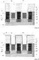
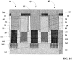
- FIG. 14 is a cross-sectional view of an intermediate stage of a semiconductor structure in step S108 according to other embodiments of the present invention.
- a second conductive material 52 is deposited on the semiconductor structure shown in FIG. 12 filling third contact hole 43.
- second conductive material 52 also fills fourth contact hole 44 and fifth contact hole 45.
- embodiments of the present invention provide a method of manufacturing a semiconductor device.
- the method may further include performing a planarization (e.g., using a chemical mechanical polishing) process after the formation of the contacts to expose a surface of the contacts, e.g., the upper surfaces of first contact 61 and second contact 62.
- a planarization e.g., using a chemical mechanical polishing
- the method includes planarizing the semiconductor structure in FIG. 13 or FIG. 14 to expose the surfaces of the first and second contacts.
- the method of manufacturing a semiconductor device can prevent unintended connections between contacts.
- the method of the present invention can prevent an electrical connection between first contact 61 of first gate 111 and third contact 63 of contact member 21, and prevent an electrical connection between third contact 63 of contact member 21 and second contact 62 of second gate 121, thereby improving the device reliability.
- the method not only can be applied to the manufacturing of FinFET devices, but also can be applied to planar devices.
- the present invention is not limited to FinFET devices.
- Embodiments of the present invention may also provide a semiconductor device.
- the semiconductor device may include an active region 24 including a first doped region 241.
- the first doped region may be a source or a drain of a CMOS device.
- the active region may include a semiconductor material, e.g., silicon.
- active region 24 may be a semiconductor fin.
- active region 24 may include a second doped region 242 and a third doped region 243 separated from first doped region 241.
- first doped region 241 is a drain
- each of second doped region 242 and third doped region 243 is a source, i.e., the semiconductor device includes two CMOS devices sharing a single source.
- first doped region 241 is a source
- each of second doped region 242 and third doped region 243 is a drain, i.e., the semiconductor device includes two CMOS devices sharing a single drain.
- the semiconductor device of FIG. 12 may be a portion of a fin-type semiconductor structure, i.e., the active region may include a plurality of doped regions each including the first, second, and third doped regions.
- the semiconductor device may further include a first contact member 21 of first doped region 241 on active region 24.
- the first contact member may include a metal such as tungsten.
- the semiconductor device may further include a plurality of gate structures on active region 24.
- the plurality of gate structures include at least first gate structure 11 and second gate structure 12 adjacent to each other.
- First gate structure 11 may include a first gate 111.
- Second gate structure 12 may include a second gate 121.
- First gate structure 11 and second gate structure 12 are disposed on opposite sides of first contact member 21.
- the first and second gate structures may include polysilicon or metals such as tungsten, aluminum and the like.
- active region 24 may be a semiconductor fin, and each of the gate structures surrounds a portion of the semiconductor fin.
- first gate structure 11 may also include a first gate insulator 112 on active region 24.
- First gate 111 is on first gate insulator 112.
- second gate structure 12 may also include a second gate insulator 122 on active region 24.
- Second gate 121 is on second gate insulator 122.
- the first and second gate insulators each may include silicon dioxide.
- the semiconductor device may also include an interlayer dielectric layer 25 on active region, interlayer dielectric layer 25 surrounds first gate structure 11, second gate structure 12, and first contact member 21.
- the interlayer dielectric layer may include silicon nitride.
- interlayer dielectric layer 25 has a portion disposed between first contact member 21 and first gate structure 11 and a portion disposed between first contact member 21 and second gate structure 12.
- interlayer dielectric layer 25 has an upper surface flush with the upper surface of first contact member 21.
- the semiconductor device may also include a contact 61 on the upper surface of first gate 111, and a second contact 62 on the upper surface of second gate 121.
- first contact 61 and second contact 62 each have a width greater than the widths of the corresponding gates.
- the width of first contact 61 is greater than the width of first gate 111
- the width of second contact 62 is greater than the width of second gate 121, as shown in FIG. 12 .
- the first and second contacts each include a metal such as tungsten.
- the semiconductor device may further include a second insulator layer 32 surrounding sidewalls of first contact 61 and second contact 62.
- First contact 61 and second contact 62 each have an upper surface lower than the upper surface of second insulator layer 32.
- the second insulator layer includes silicon nitride.
- the semiconductor device may also include a third insulator layer 33 covering the upper surfaces of first contact 61 and second contact 62.
- the third insulator layer includes silicon nitride.
- the semiconductor device may also include a first insulator layer 31 on interlayer dielectric layer 25 and surrounding at least a portion of second insulator layer 32 and at least a portion of third insulator layer 33.
- First insulator layer 31 has a third contact hole 43 that exposes at least a surface portion of first contact member 21.
- the first insulator layer includes silicon dioxide.
- first insulator layer 31 also has a fourth contact hole 44 that exposes at least a surface portion of second contact 22 and a fifth contact hole 45 that exposes at least a surface portion of third contact 23.
- the semiconductor device may also include a fourth insulator layer 26 surrounding active region 24, interlayer dielectric layer 25 and contact members 21, 21, and 23.
- First insulator layer 31 has a portion disposed on fourth insulator layer 26.
- the fourth insulator layer may include silicon dioxide.
- the semiconductor device may also include a buffer layer 711 disposed on first insulator layer 31, second insulator layer 32, and third insulator 33.
- contacts can be formed in corresponding contact holes that have no electrical connections with each other, thereby improving the device reliability.
- embodiments of the present invention provide a detailed description of a method of manufacturing a semiconductor device and a semiconductor device manufactured by the described method. Details of well-known processes are omitted in order not to obscure the concepts presented herein.
Landscapes
- Electrodes Of Semiconductors (AREA)
- Insulated Gate Type Field-Effect Transistor (AREA)
- Internal Circuitry In Semiconductor Integrated Circuit Devices (AREA)
Applications Claiming Priority (1)
| Application Number | Priority Date | Filing Date | Title |
|---|---|---|---|
| CN201610379201.6A CN107452680B (zh) | 2016-06-01 | 2016-06-01 | 半导体装置及其制造方法 |
Publications (1)
| Publication Number | Publication Date |
|---|---|
| EP3255677A1 true EP3255677A1 (de) | 2017-12-13 |
Family
ID=58994869
Family Applications (1)
| Application Number | Title | Priority Date | Filing Date |
|---|---|---|---|
| EP17173739.8A Withdrawn EP3255677A1 (de) | 2016-06-01 | 2017-05-31 | Verfahren zur herstellung einer finfet-vorrichtung |
Country Status (3)
| Country | Link |
|---|---|
| US (2) | US10008495B2 (de) |
| EP (1) | EP3255677A1 (de) |
| CN (1) | CN107452680B (de) |
Families Citing this family (3)
| Publication number | Priority date | Publication date | Assignee | Title |
|---|---|---|---|---|
| CN107452680B (zh) | 2016-06-01 | 2020-05-05 | 中芯国际集成电路制造(上海)有限公司 | 半导体装置及其制造方法 |
| US11210447B2 (en) * | 2018-09-26 | 2021-12-28 | Taiwan Semiconductor Manufacturing Co., Ltd. | Reconfiguring layout and sizing for transistor components to simultaneously optimize logic devices and non-logic devices |
| US12538790B2 (en) * | 2023-08-11 | 2026-01-27 | Nanya Technology Corporation | Electrical structure and method of manufacturing the same |
Citations (8)
| Publication number | Priority date | Publication date | Assignee | Title |
|---|---|---|---|---|
| US20040173912A1 (en) * | 2003-03-04 | 2004-09-09 | Rhodes Howard E. | Damascene processes for forming conductive structures |
| US20070099363A1 (en) * | 2005-09-28 | 2007-05-03 | Kazuaki Nakajima | Method of manufacturing semiconductor device |
| US20120313153A1 (en) * | 2011-06-13 | 2012-12-13 | International Business Machines | System and method of plating conductive gate contacts on metal gates for self-aligned contact interconnections |
| US20130200461A1 (en) * | 2012-02-08 | 2013-08-08 | Taiwan Semiconductor Manufacturing Company, Ltd. | Semiconductor Device and Method of Forming the Same |
| US9111962B1 (en) * | 2014-03-20 | 2015-08-18 | International Business Machines Corporation | Selective dielectric spacer deposition for exposing sidewalls of a finFET |
| US20150235948A1 (en) * | 2014-02-14 | 2015-08-20 | Qualcomm Incorporated | Grounding dummy gate in scaled layout design |
| US20150270171A1 (en) * | 2014-03-24 | 2015-09-24 | International Business Machines Corporation | Dielectric liner for a self-aligned contact via structure |
| US20160005822A1 (en) * | 2014-07-01 | 2016-01-07 | Qualcomm Incorporated | Self-aligned via for gate contact of semiconductor devices |
Family Cites Families (18)
| Publication number | Priority date | Publication date | Assignee | Title |
|---|---|---|---|---|
| KR100464416B1 (ko) * | 2002-05-14 | 2005-01-03 | 삼성전자주식회사 | 증가된 유효 채널 길이를 가지는 반도체 소자의 제조 방법 |
| CN104218082B (zh) * | 2013-06-04 | 2017-08-25 | 中芯国际集成电路制造(上海)有限公司 | 高迁移率鳍型场效应晶体管及其制造方法 |
| KR20140145419A (ko) * | 2013-06-13 | 2014-12-23 | 삼성전자주식회사 | 반도체 소자 제조 방법 |
| US9312354B2 (en) * | 2014-02-21 | 2016-04-12 | Taiwan Semiconductor Manufacturing Company, Ltd. | Contact etch stop layers of a field effect transistor |
| US9711646B2 (en) * | 2014-03-31 | 2017-07-18 | United Microelectronics Corp. | Semiconductor structure and manufacturing method for the same |
| JP2015220420A (ja) * | 2014-05-21 | 2015-12-07 | 富士通セミコンダクター株式会社 | 半導体装置の製造方法および半導体装置 |
| US20160049401A1 (en) * | 2014-08-13 | 2016-02-18 | Globalfoundries Inc. | Hybrid contacts for commonly fabricated semiconductor devices using same metal |
| US9397003B1 (en) * | 2015-05-27 | 2016-07-19 | Globalfoundries Inc. | Method for forming source/drain contacts during CMOS integration using confined epitaxial growth techniques |
| CN106340455B (zh) * | 2015-07-06 | 2021-08-03 | 联华电子股份有限公司 | 半导体元件及其制作方法 |
| US9870953B2 (en) * | 2015-10-26 | 2018-01-16 | International Business Machines Corporation | System on chip material co-integration |
| CN113659004B (zh) * | 2015-11-26 | 2023-12-19 | 联华电子股份有限公司 | 半导体元件及其制作方法 |
| US9887289B2 (en) * | 2015-12-14 | 2018-02-06 | International Business Machines Corporation | Method and structure of improving contact resistance for passive and long channel devices |
| US9653364B1 (en) * | 2016-01-08 | 2017-05-16 | Taiwan Semiconductor Manufacturing Co., Ltd. | FinFET device and method of forming the same |
| US9824920B2 (en) * | 2016-04-04 | 2017-11-21 | Globalfoundries Inc. | Methods of forming self-aligned contact structures by work function material layer recessing and the resulting devices |
| KR102514620B1 (ko) * | 2016-04-28 | 2023-03-29 | 삼성전자주식회사 | 반도체 소자 및 이의 제조 방법 |
| US9793372B1 (en) * | 2016-05-25 | 2017-10-17 | Globalfoundries Inc. | Integrated circuit including a dummy gate structure and method for the formation thereof |
| CN107452680B (zh) | 2016-06-01 | 2020-05-05 | 中芯国际集成电路制造(上海)有限公司 | 半导体装置及其制造方法 |
| CN107564953B (zh) * | 2016-07-01 | 2021-07-30 | 中芯国际集成电路制造(上海)有限公司 | 变容晶体管及其制造方法 |
-
2016
- 2016-06-01 CN CN201610379201.6A patent/CN107452680B/zh active Active
-
2017
- 2017-04-10 US US15/483,554 patent/US10008495B2/en active Active
- 2017-05-31 EP EP17173739.8A patent/EP3255677A1/de not_active Withdrawn
-
2018
- 2018-05-29 US US15/991,332 patent/US10347629B2/en active Active
Patent Citations (8)
| Publication number | Priority date | Publication date | Assignee | Title |
|---|---|---|---|---|
| US20040173912A1 (en) * | 2003-03-04 | 2004-09-09 | Rhodes Howard E. | Damascene processes for forming conductive structures |
| US20070099363A1 (en) * | 2005-09-28 | 2007-05-03 | Kazuaki Nakajima | Method of manufacturing semiconductor device |
| US20120313153A1 (en) * | 2011-06-13 | 2012-12-13 | International Business Machines | System and method of plating conductive gate contacts on metal gates for self-aligned contact interconnections |
| US20130200461A1 (en) * | 2012-02-08 | 2013-08-08 | Taiwan Semiconductor Manufacturing Company, Ltd. | Semiconductor Device and Method of Forming the Same |
| US20150235948A1 (en) * | 2014-02-14 | 2015-08-20 | Qualcomm Incorporated | Grounding dummy gate in scaled layout design |
| US9111962B1 (en) * | 2014-03-20 | 2015-08-18 | International Business Machines Corporation | Selective dielectric spacer deposition for exposing sidewalls of a finFET |
| US20150270171A1 (en) * | 2014-03-24 | 2015-09-24 | International Business Machines Corporation | Dielectric liner for a self-aligned contact via structure |
| US20160005822A1 (en) * | 2014-07-01 | 2016-01-07 | Qualcomm Incorporated | Self-aligned via for gate contact of semiconductor devices |
Also Published As
| Publication number | Publication date |
|---|---|
| US20180294262A1 (en) | 2018-10-11 |
| CN107452680A (zh) | 2017-12-08 |
| US10008495B2 (en) | 2018-06-26 |
| US20170352658A1 (en) | 2017-12-07 |
| US10347629B2 (en) | 2019-07-09 |
| CN107452680B (zh) | 2020-05-05 |
Similar Documents
| Publication | Publication Date | Title |
|---|---|---|
| US11081356B2 (en) | Method for metal gate cut and structure thereof | |
| US11251086B2 (en) | Semiconductor devices, FinFET devices, and manufacturing methods thereof | |
| TWI584478B (zh) | 半導體裝置及其製造方法 | |
| US9136178B2 (en) | Method for fabricating a finFET in a large scale integrated circuit | |
| KR101637679B1 (ko) | Fⅰnfet을 형성하기 위한 메커니즘들을 포함하는 반도체 디바이스및 그 형성 방법 | |
| US12191380B2 (en) | Semiconductor device and method | |
| US11581410B2 (en) | Semiconductor device and method | |
| CN111106160B (zh) | 半导体器件及其制造方法及包括该器件的电子设备 | |
| EP3258498B1 (de) | Ldmos-entwurf für eine finfet-vorrichtung | |
| CN107045980B (zh) | 晶体管的形成方法 | |
| US12068371B2 (en) | Method for FinFET LDD doping | |
| US20200176326A1 (en) | Semiconductor Device and Method | |
| EP3258499A1 (de) | Ldmos-finfet-vorrichtung | |
| WO2014071651A1 (zh) | 半导体器件及其制造方法 | |
| EP3316286A1 (de) | Dummy-gatestrukturen und verfahren zu ihrer herstellung | |
| US20010034109A1 (en) | Trench seimconductor devices reduced trench pitch | |
| EP3255654A1 (de) | Halbleiterbauelement und herstellungsverfahren dafür | |
| US20220384270A1 (en) | Semiconductor Device and Method | |
| US10347629B2 (en) | FinFET device | |
| US20230131688A1 (en) | Nanosheet channel formation method and structure | |
| CN108074974B (zh) | 半导体装置的形成方法 | |
| EP3252826A1 (de) | Verfahren und vorrichtung für verbindungshalbleiterrippenstruktur | |
| US20250344420A1 (en) | Nanostructure field-effect transistor device and methods of forming | |
| CN117253798A (zh) | Ldmos器件及其制造方法 |
Legal Events
| Date | Code | Title | Description |
|---|---|---|---|
| PUAI | Public reference made under article 153(3) epc to a published international application that has entered the european phase |
Free format text: ORIGINAL CODE: 0009012 |
|
| STAA | Information on the status of an ep patent application or granted ep patent |
Free format text: STATUS: THE APPLICATION HAS BEEN PUBLISHED |
|
| AK | Designated contracting states |
Kind code of ref document: A1 Designated state(s): AL AT BE BG CH CY CZ DE DK EE ES FI FR GB GR HR HU IE IS IT LI LT LU LV MC MK MT NL NO PL PT RO RS SE SI SK SM TR |
|
| AX | Request for extension of the european patent |
Extension state: BA ME |
|
| STAA | Information on the status of an ep patent application or granted ep patent |
Free format text: STATUS: REQUEST FOR EXAMINATION WAS MADE |
|
| 17P | Request for examination filed |
Effective date: 20180523 |
|
| RBV | Designated contracting states (corrected) |
Designated state(s): AL AT BE BG CH CY CZ DE DK EE ES FI FR GB GR HR HU IE IS IT LI LT LU LV MC MK MT NL NO PL PT RO RS SE SI SK SM TR |
|
| RAP1 | Party data changed (applicant data changed or rights of an application transferred) |
Owner name: SEMICONDUCTOR MANUFACTURING INTERNATIONAL (BEIJING Owner name: SEMICONDUCTOR MANUFACTURING INTERNATIONAL (SHANGHA |
|
| RIC1 | Information provided on ipc code assigned before grant |
Ipc: H01L 21/8234 20060101ALI20190226BHEP Ipc: H01L 29/417 20060101AFI20190226BHEP Ipc: H01L 21/768 20060101ALI20190226BHEP |
|
| STAA | Information on the status of an ep patent application or granted ep patent |
Free format text: STATUS: EXAMINATION IS IN PROGRESS |
|
| 17Q | First examination report despatched |
Effective date: 20200610 |
|
| STAA | Information on the status of an ep patent application or granted ep patent |
Free format text: STATUS: THE APPLICATION IS DEEMED TO BE WITHDRAWN |
|
| 18D | Application deemed to be withdrawn |
Effective date: 20201021 |