EP3251173B1 - Steckverbinderanordnung mit hülsenteil - Google Patents
Steckverbinderanordnung mit hülsenteil Download PDFInfo
- Publication number
- EP3251173B1 EP3251173B1 EP16701257.4A EP16701257A EP3251173B1 EP 3251173 B1 EP3251173 B1 EP 3251173B1 EP 16701257 A EP16701257 A EP 16701257A EP 3251173 B1 EP3251173 B1 EP 3251173B1
- Authority
- EP
- European Patent Office
- Prior art keywords
- plug connector
- wire
- wires
- cable
- sleeve part
- Prior art date
- Legal status (The legal status is an assumption and is not a legal conclusion. Google has not performed a legal analysis and makes no representation as to the accuracy of the status listed.)
- Active
Links
- 239000004020 conductor Substances 0.000 claims description 72
- 238000009413 insulation Methods 0.000 claims description 8
- 239000012212 insulator Substances 0.000 claims description 7
- 230000001965 increasing effect Effects 0.000 claims description 6
- 239000000463 material Substances 0.000 claims description 6
- 239000012811 non-conductive material Substances 0.000 claims description 6
- 239000004033 plastic Substances 0.000 claims description 4
- 229920003023 plastic Polymers 0.000 claims description 4
- 125000006850 spacer group Chemical group 0.000 claims description 4
- 230000007704 transition Effects 0.000 description 8
- 230000013011 mating Effects 0.000 description 4
- 230000006978 adaptation Effects 0.000 description 3
- 238000002788 crimping Methods 0.000 description 2
- 230000000694 effects Effects 0.000 description 2
- 239000011888 foil Substances 0.000 description 2
- 230000006872 improvement Effects 0.000 description 2
- 230000001939 inductive effect Effects 0.000 description 2
- 239000002184 metal Substances 0.000 description 2
- 230000008054 signal transmission Effects 0.000 description 2
- 230000009471 action Effects 0.000 description 1
- 230000008901 benefit Effects 0.000 description 1
- 230000005540 biological transmission Effects 0.000 description 1
- 230000008859 change Effects 0.000 description 1
- 238000010276 construction Methods 0.000 description 1
- 230000001419 dependent effect Effects 0.000 description 1
- 238000011161 development Methods 0.000 description 1
- 230000018109 developmental process Effects 0.000 description 1
- 239000003989 dielectric material Substances 0.000 description 1
- 230000001681 protective effect Effects 0.000 description 1
- 230000009467 reduction Effects 0.000 description 1
- 238000005476 soldering Methods 0.000 description 1
- 230000007480 spreading Effects 0.000 description 1
Images

Classifications
-
- H—ELECTRICITY
- H01—ELECTRIC ELEMENTS
- H01R—ELECTRICALLY-CONDUCTIVE CONNECTIONS; STRUCTURAL ASSOCIATIONS OF A PLURALITY OF MUTUALLY-INSULATED ELECTRICAL CONNECTING ELEMENTS; COUPLING DEVICES; CURRENT COLLECTORS
- H01R13/00—Details of coupling devices of the kinds covered by groups H01R12/70 or H01R24/00 - H01R33/00
- H01R13/648—Protective earth or shield arrangements on coupling devices, e.g. anti-static shielding
- H01R13/658—High frequency shielding arrangements, e.g. against EMI [Electro-Magnetic Interference] or EMP [Electro-Magnetic Pulse]
- H01R13/6581—Shield structure
-
- H—ELECTRICITY
- H01—ELECTRIC ELEMENTS
- H01R—ELECTRICALLY-CONDUCTIVE CONNECTIONS; STRUCTURAL ASSOCIATIONS OF A PLURALITY OF MUTUALLY-INSULATED ELECTRICAL CONNECTING ELEMENTS; COUPLING DEVICES; CURRENT COLLECTORS
- H01R13/00—Details of coupling devices of the kinds covered by groups H01R12/70 or H01R24/00 - H01R33/00
- H01R13/58—Means for relieving strain on wire connection, e.g. cord grip, for avoiding loosening of connections between wires and terminals within a coupling device terminating a cable
- H01R13/582—Means for relieving strain on wire connection, e.g. cord grip, for avoiding loosening of connections between wires and terminals within a coupling device terminating a cable the cable being clamped between assembled parts of the housing
- H01R13/5825—Means for relieving strain on wire connection, e.g. cord grip, for avoiding loosening of connections between wires and terminals within a coupling device terminating a cable the cable being clamped between assembled parts of the housing the means comprising additional parts captured between housing parts and cable
-
- H—ELECTRICITY
- H01—ELECTRIC ELEMENTS
- H01R—ELECTRICALLY-CONDUCTIVE CONNECTIONS; STRUCTURAL ASSOCIATIONS OF A PLURALITY OF MUTUALLY-INSULATED ELECTRICAL CONNECTING ELEMENTS; COUPLING DEVICES; CURRENT COLLECTORS
- H01R4/00—Electrically-conductive connections between two or more conductive members in direct contact, i.e. touching one another; Means for effecting or maintaining such contact; Electrically-conductive connections having two or more spaced connecting locations for conductors and using contact members penetrating insulation
- H01R4/10—Electrically-conductive connections between two or more conductive members in direct contact, i.e. touching one another; Means for effecting or maintaining such contact; Electrically-conductive connections having two or more spaced connecting locations for conductors and using contact members penetrating insulation effected solely by twisting, wrapping, bending, crimping, or other permanent deformation
- H01R4/18—Electrically-conductive connections between two or more conductive members in direct contact, i.e. touching one another; Means for effecting or maintaining such contact; Electrically-conductive connections having two or more spaced connecting locations for conductors and using contact members penetrating insulation effected solely by twisting, wrapping, bending, crimping, or other permanent deformation by crimping
- H01R4/20—Electrically-conductive connections between two or more conductive members in direct contact, i.e. touching one another; Means for effecting or maintaining such contact; Electrically-conductive connections having two or more spaced connecting locations for conductors and using contact members penetrating insulation effected solely by twisting, wrapping, bending, crimping, or other permanent deformation by crimping using a crimping sleeve
-
- H—ELECTRICITY
- H01—ELECTRIC ELEMENTS
- H01R—ELECTRICALLY-CONDUCTIVE CONNECTIONS; STRUCTURAL ASSOCIATIONS OF A PLURALITY OF MUTUALLY-INSULATED ELECTRICAL CONNECTING ELEMENTS; COUPLING DEVICES; CURRENT COLLECTORS
- H01R13/00—Details of coupling devices of the kinds covered by groups H01R12/70 or H01R24/00 - H01R33/00
- H01R13/646—Details of coupling devices of the kinds covered by groups H01R12/70 or H01R24/00 - H01R33/00 specially adapted for high-frequency, e.g. structures providing an impedance match or phase match
- H01R13/6461—Means for preventing cross-talk
- H01R13/6463—Means for preventing cross-talk using twisted pairs of wires
-
- H—ELECTRICITY
- H01—ELECTRIC ELEMENTS
- H01R—ELECTRICALLY-CONDUCTIVE CONNECTIONS; STRUCTURAL ASSOCIATIONS OF A PLURALITY OF MUTUALLY-INSULATED ELECTRICAL CONNECTING ELEMENTS; COUPLING DEVICES; CURRENT COLLECTORS
- H01R13/00—Details of coupling devices of the kinds covered by groups H01R12/70 or H01R24/00 - H01R33/00
- H01R13/646—Details of coupling devices of the kinds covered by groups H01R12/70 or H01R24/00 - H01R33/00 specially adapted for high-frequency, e.g. structures providing an impedance match or phase match
- H01R13/6473—Impedance matching
-
- H—ELECTRICITY
- H01—ELECTRIC ELEMENTS
- H01R—ELECTRICALLY-CONDUCTIVE CONNECTIONS; STRUCTURAL ASSOCIATIONS OF A PLURALITY OF MUTUALLY-INSULATED ELECTRICAL CONNECTING ELEMENTS; COUPLING DEVICES; CURRENT COLLECTORS
- H01R13/00—Details of coupling devices of the kinds covered by groups H01R12/70 or H01R24/00 - H01R33/00
- H01R13/648—Protective earth or shield arrangements on coupling devices, e.g. anti-static shielding
- H01R13/658—High frequency shielding arrangements, e.g. against EMI [Electro-Magnetic Interference] or EMP [Electro-Magnetic Pulse]
- H01R13/6591—Specific features or arrangements of connection of shield to conductive members
- H01R13/65912—Specific features or arrangements of connection of shield to conductive members for shielded multiconductor cable
- H01R13/65915—Twisted pair of conductors surrounded by shield
-
- H—ELECTRICITY
- H01—ELECTRIC ELEMENTS
- H01R—ELECTRICALLY-CONDUCTIVE CONNECTIONS; STRUCTURAL ASSOCIATIONS OF A PLURALITY OF MUTUALLY-INSULATED ELECTRICAL CONNECTING ELEMENTS; COUPLING DEVICES; CURRENT COLLECTORS
- H01R2103/00—Two poles
Definitions
- the invention relates to a connector arrangement with a connector and a cable connected to it with at least one wire pair for transmitting a differential signal, the wires of the wire pair having a first mutual distance X in a sheathed cable section, diverging in a widening section in the direction of the connector and in one Guide section of the connector have a larger second mutual distance Y.
- At least one wire pair for the transmission of a differential signal runs in the cable, the wires of the wire pair being at a first mutual distance inside the cable.
- This first mutual distance can result from the fact that the wire pair is covered by an outer cable layer such as an outer conductor (for example a wire mesh or a foil shield), an insulator and / or a protective jacket or the like. is sheathed, which rests on the outside of the pair of wires and holds the pair of wires under the first distance inside the cable.
- the mutual wire spacing is measured perpendicular to the longitudinal direction of the cable between the centers of the two wires.
- the two wires of the wire pair run from the sheathed cable section in the direction of the connector in a widening section until they run into a guide section of the connector in which they have a second mutual distance which is greater than the first mutual distance.
- the connector has a plug-side end for connecting the connector to a mating connector and a cable-side end on which the cable For example. Is attached by soldering and / or crimping.
- the wires of the wire pair can be electrically connected to inner conductor contact elements of the connector within the connector.
- the cable is, for example, a twisted pair cable with one or more pairs of wires twisted with one another, each of which is used to transmit a differential signal such as a data signal, telecommunications signal, RF signal or the like. are set up. Due to the twisting, better protection against external fields can be achieved.
- the cable has more than two differential wire pairs and is, for example, a star quad cable or the like.
- FIG Fig. 1 A conventional connector assembly 200 with a wire pair 222 having a cable 220 that is connected to a connector 210 is shown in FIG Fig. 1 shown.
- the wires of the wire pair 222 in the cable interior 232 have a first mutual spacing X and in the interior of an insulator part 216 of the plug connector 210 a second mutual spacing Y.
- the two wires of wire pair 222 diverge in a widening section 234.
- an electrical connector which is connected to a multi-core cable.
- the wires of a cable are guided out of an insulating jacket and, with increasing mutual spacing, over a widening section to a guide section.
- a dielectric element is provided in the widened section and in the guide section, but only in the guide section exercises a slight radial guidance on contact pins which are electrically and mechanically connected to the wires of the cable. In the widened section, there is no radial guidance of the cable wires that have been freed from the insulating jacket.
- a plug connector for several conductors of a cable is known, the plug connector providing a termination and a clamping holder for the conductors of the cable that have been freed from the insulating jacket of the cable, but each individually electrically insulated.
- a conductor carrier is provided which has a cylindrical shape and axially on its circumference Has grooves running in the direction, which are designed to receive an insulated line in each case.
- the conductor carrier is conically tapered.
- the conductor carrier is designed in such a way that it guides the lines in the grooves with a mutual spacing which is greater than the mutual spacing of the conductors within the insulating jacket of the cable.
- the conductors run apart with increasing mutual spacing.
- the conductors diverge, the conductors are only partially supported radially from the inside, but the conductors are not guided radially from the outside.
- the object of the present invention is to improve the signal transmission at a transition between a cable and a connector, in particular in the high-frequency range, and to minimize interference.
- a sleeve part at least partially encircling the wire pair in the widening section is provided for at least partially exerting pressure from radially outside on the wires of the wire pair in the widening section in order to reduce the distance between them.
- the invention is based on the knowledge that the characteristic impedance or the impedance both inside the cable and inside the connector due to the geometry or the mutual arrangement of the wires of the wire pair in Combination with the interposed dielectric is set up to a predetermined and as uniform as possible value, while abrupt changes in the characteristic impedance can occur at the transition point between the cable and the connector due to the changing distance between the wires and the changing dielectric. Such abrupt changes such as jumps, fluctuations and other irregularities can lead to the disturbances described above, such as signal reflections. It is therefore advantageous to shorten the area of a changing wire spacing in the longitudinal direction of the cable and to set up the wire pair geometry in this area in such a way that a jump in the wave resistance is reduced or avoided.
- the two wires in the widening section are pressed together by a sleeve part surrounding the wire pair in order to reduce the distance between them.
- the sleeve part exerts pressure on the wire pair from the radial outside, so that the first wire spacing is continued in the direction of the guide section of the connector even where the wire pair is no longer sheathed by an outer layer of the cable.
- the connector arrangement according to the invention can be set up in a shielded or unshielded manner.
- the cable has an outer conductor surrounding the pair of wires, such as a wire mesh
- the connector has an outer conductor part surrounding the inner conductor contacts, such as an outer conductor housing.
- the wire pair is preferably also surrounded in the widened section by a shielding such as a metallic sleeve section of the plug connector.
- the cable and / or the connector has no outer conductor or no outer conductor part.
- the sleeve part is a sleeve that completely encircles the wire pair, such as a closed cylindrical jacket sleeve. Such a sleeve can be pushed from the cable in the direction of the guide section during the assembly of the connector assembly until it at least partially compresses the cores diverging in the widening section and is held there in a form-fitting and / or force-fitting manner.
- the sleeve part can also be made from there are two or more interconnected sleeve shells that are placed on the wire pair from different sides.
- the sleeve part has an inner surface which is inclined with respect to the longitudinal direction of the cable, in particular a conical or convex inner surface.
- the wire pair can be guided apart exactly with an intended degree of curvature and / or in a desired course, which has proven to be sensible with regard to a course of the wave resistance that is as constant as possible.
- the inner diameter of the sleeve part is adapted at its cable-side end approximately to the first distance and at its connector-side end is adapted approximately to the second distance.
- the sleeve part has approximately the same inner diameter at its cable-side end as a wire pair sheathing in the sheathed cable section. This inside diameter can correspond to the first distance plus the simple wire diameter.
- the inner diameter of the sleeve part at its connector-side end can correspond to the second distance plus the simple wire diameter.
- the sleeve part is preferably arranged and shaped in such a way that, after exiting the sheathed cable cutout, the wires continue to run in parallel with essentially the first mutual spacing and then diverge in the widening section with increased curvature in the direction of the guide section until they with enlarged distance in turn run essentially parallel into the guide section of the connector.
- the sleeve part is radially deformed by the action of pressure from the outside, in particular pressed against the wire pair, for example pressed or crimped, in order to further reduce the distance between the wires of the wire pair running through the sleeve part.
- a preferably non-conductive spacer such as a mandrel, which extends from the connector into the widened section and is arranged between the wires of the wire pair and to which the wires are pressed by the sleeve part.
- the mandrel can prevent the sleeve part from being deformed too much and thus from compressing the wires too much.
- the material of the mandrel can be selected in such a way that a predetermined profile of the wave resistance results in the widened section.
- the mandrel can consist of a non-conductive material such as a plastic material or another dielectric or insulator material.
- a mandrel made of a non-conductive material has the further advantage that the two wires cannot come into electrical contact when they are pressed together, even if the wire insulation in the widened section is missing in sections.
- the sleeve part can also be formed from a non-conductive material such as a plastic material.
- the material of the sleeve part can be selected in such a way that a predetermined profile of the wave resistance results in the widened section.
- the cable has an outer conductor that encircles the pair of wires, such as a wire mesh or foil shield, which provides a shield for the at least one pair of wires.
- the connector also has an outer conductor part, for example in the form of an outer conductor housing made of a conductive material, which is electrically connected to the outer conductor.
- the outer conductor part can have a sleeve section protruding in the direction of the cable, which runs around the wire pair and the sleeve part in the widening section and rests on the outside of the outer conductor of the cable.
- the outer conductor of the cable which is preferably designed as a wire mesh, is preferably pressed or crimped directly or indirectly to the outer conductor part of the plug connector.
- the wire mesh can be wrapped around a crimp sleeve attached to the front end of the sheathed cable section.
- the crimp sleeve or the outer conductor folded around it preferably forms the connector-side end of the sheathed cable section.
- the sleeve part at least at its cable-side end has approximately the same inner diameter as the outer conductor of the cable, so that it is shielded of the wire pair continues in the direction of the connector.
- the sleeve part is formed from an electrically conductive material such as metal.
- the shielding is continued by the sleeve part starting from the front axial end of the outer conductor at an approximately constant distance to the wire pair, so that there is no sudden change in impedance in this area.
- the connector has an insulator part with guide channels for the wires of the wire pair that are spaced transversely to the longitudinal direction of the cable and through which the guide section is formed.
- the wires of the wire pair can be connected, in particular crimped, at their connector-side ends to the inner conductor contact elements of the connector.
- the mutual spacing is regular of the wires is still too large, at least in sections, so that an optimal electrical adaptation at the transition between the widening section and the guide section of the connector has not yet been achieved.
- the distance between the two wires at this transition can be further reduced by at least sections of the front ends of the wires protruding into the guide section being encircled by a wire sleeve made of an electrically conductive material adjacent to the widening section.
- the wire sleeves are each in electrical contact with the conductor of the associated wire and preferably run around the wire completely.
- the wire sleeves can be crimped onto the wire conductor and / or the wire insulation (ISO crimp). Crimping onto the core insulation leads to a particularly large reduction in the distance between the two core conductors.
- the wires can be connected to the inner conductor contact elements of the connector by means of the wire sleeves.
- the wire sleeves can also reduce the distance between the individual wires and a common outer conductor part which may encircle the wires, whereby the course of the wave resistance over the spreading section can be further improved.
- each wire sleeve facing the widening section surrounds the wire insulation, and the other end of each wire sleeve surrounds the wire conductor directly, makes electrical contact with it and connects it to the inner conductor contact element of the connector.
- the end of the wire sleeve facing the widening section is preferably crimped on the outside of the wire insulation (ISO crimp), and the connector-side end of the wire sleeve is crimped onto the wire conductor. This leads to a particularly high tensile strength connection between the wire pair and the inner conductor contact elements of the connector with optimal electrical adaptation.
- FIG. 1 and 2 are a conventional ( Fig. 1 ) and an inventive ( Fig. 2 ) Connector arrangement opposite each other.
- the connector arrangement 100 according to the invention shown consists of a connector 10 and a cable 20 fastened thereto in a tensile manner, such as a shielded twisted pair cable or a star quad cable with two differential wire pairs.
- the cable 20 is connected to the cable-side end of the connector 10, while a mating connector 80 is detachably plugged into the plug-in end of the connector 10.
- the cable 20 is a shielded twisted pair cable with a twisted pair of wires 22, 24 and an outer conductor 26 that encircles the pair of wires 22, 24 and can be in the form of a wire mesh.
- the two wires 22, 24 run along the longitudinal direction L of the cable at a predetermined distance X.
- a cable is particularly suitable for transmitting a differential signal such as an RF signal, a data signal, a telecommunication signal, etc.
- a predetermined impedance curve over the entire extension of the connector arrangement in FIG Cable longitudinal direction L. In particular, large variations or fluctuations in the characteristic impedance, impedance jumps, etc. are undesirable.
- the cable can also have more than one wire pair.
- the cable has two or more wire pairs stranded with one another, possibly in a star quad arrangement, which can be surrounded by a common outer conductor for shielding.
- the two wires 22, 24 diverge in a widening section 34 until they run into a guide section 36 of the connector 10.
- the wires 22, 24 are each arranged in a guide channel of an insulator part 14, by means of which a predetermined larger second distance Y between the two wires 22, 24 is ensured.
- the wires 22, 24 are each electrically connected to inner conductor contact elements 16 of the plug connector 10.
- the inner conductor contact elements 16 of the connector are set up for electrical contacting of inner conductor mating contact elements of the mating connector 80.
- the wire pair is at least partially encircled by a sleeve part 40 which exerts pressure on the wires from the outside and in this way reduces the distance between them.
- the sleeve part 40 can have a cylindrical outer surface and a substantially conical inner surface 42, the conical inner surface lying closely against the wires 22, 24 and compressing them together.
- the sleeve part 40 can be deformed by exerting pressure from the outside. Alternatively or additionally, the sleeve part is clamped onto the wire pair.
- a spacer 44 tapering in the direction of the sheathed cable section 32 such as a mandrel, is provided between the two wires 22, 24, against which the two wires 22, 24 are pressed from the outside.
- the course of the outer surface of the mandrel 44 in the longitudinal direction L of the cable can be adapted to the inner surface 42 of the sleeve part 40, so that suitable free spaces are formed in between for the wires 22, 24.
- the mandrel 44 is preferably made of a non-conductive material such as a dielectric material. This has been a desired one in terms of one Impedance curve and, on the other hand, to prevent electrical contacting of the two wires 22, 24 have proven to be particularly expedient.
- the mandrel 44 may be integrally connected to the connector 10. For example, the mandrel 44 is attached to the insulator part 14 and protrudes from there into the widened section 34.
- the inner diameter of the connector-side end of the sleeve part 40 is approximately the difference between the second distance Y and the first distance X greater than the inner diameter of the cable-side end of the sleeve part 40. This means that the wire spacing X inside the cable through the sleeve part 40 continues towards the connector continued. Only along the inner surface 42 of the sleeve part running obliquely outward do the wires 22, 24 extend outward with increased curvature until they run into the guide section 36.
- the sleeve part consists of a non-conductive material such as plastic.
- the sleeve part is made of a conductive material such as metal.
- the sleeve part 40 can continue the shielding of the wire pair following the connector-side end of the outer conductor 26 of the cable 20.
- the sleeve part 40 directly adjoins the connector-side end of the outer conductor 26.
- the wires 22, 24 of the wire pair each have a wire sleeve 60 which is arranged adjacent to the widening section 34 in the guide section 36 and which runs around the respective wire.
- the wire sleeve 60 is in each case electrically connected to the associated wire conductor. This further reduces the distance between the two core conductors at the transition between the widening section 34 and the guide section 36.
- the core sleeve is preferably crimped onto the core insulation (ISO crimp) and / or crimped onto the core conductor.
- ISO crimp core insulation
- the cable-side end of the wire sleeve 60 is crimped onto the wire insulation in order to increase the distance between the wire conductors reduce, and the other end of the wire sleeve 60 is crimped directly to the wire conductor in order to connect it to the inner conductor contact element 16 with tensile strength.
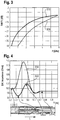
- Fig. 3 are reflection losses ("return loss") of signals as a function of the signal frequency.
- Reference numeral 310 denotes signals that are generated by the in Fig. 1
- the conventional connector assembly shown in FIG Fig. 2 shown connector assembly according to the invention are performed. It can be clearly seen that in the frequency range up to about 6 GHz, in particular between 1.5 GHz and 6 GHz, significantly fewer losses occur when using the connector arrangement according to the invention.
- the impedance curve in the longitudinal direction of the cable L in the connector arrangement according to the invention which in contrast to the conventional connector arrangement comprises a sleeve part 40 and wire sleeves 60 with ISO crimp, has fewer fluctuations.
- FIG. 4 shows the characteristic impedance as a function of the signal propagation time or as a function of the position in the longitudinal direction L of the cable.
- Reference numeral 330 denotes the in Fig. 1 Conventional connector arrangement shown without sleeve part 40 and ferrules 60, and reference numeral 340 denotes the in Fig. 2 shown connector assembly according to the invention.
- the impedance at the plug-in end of the connector is in each case approximately 100 ohms (see reference number 351) and the impedance inside the cable is approximately 99 ohms in each case (see reference number 354).
- the impedance of the conventional connector arrangement 200 passes through a pronounced maximum, which is approximately in the area of the widened section 234 (cf. reference numeral 330). This maximum leads to signal interference and reflections, as they do Fig. 3 can be seen.
- the impedance of the connector arrangement 100 according to the invention has significantly reduced fluctuations (cf. reference numeral 340).
- the area of the ISO-Crimps is now a little too capacitive (see reference number 352) and the transition between the sheathed cable section 32 and the widening section 34 is still a little too inductive (see reference number 353), albeit greatly improved. Therefore, these two effects compensate each other very well for frequencies up to about 6 GHz, but this works less well for even higher frequencies.
- a further improvement can, if necessary, be achieved through thinner-walled wire sleeves 60 and / or a smaller wire diameter in the area of the ISO crimp.
- the wires in the widening section 34 may have to be pressed together even further.
- a star crimp for exerting even greater pressure on the wire pair can additionally or alternatively be considered.
- the cable can have more than one wire pair.
- the cable is not necessarily shielded and does not necessarily have an outer conductor.
- the sleeve part can be a separate component or, alternatively, can be connected to or integrated into the connector.
- the sleeve part can be positively, non-positively and / or cohesively connected to the wire pair.
Landscapes
- Details Of Connecting Devices For Male And Female Coupling (AREA)
- Coupling Device And Connection With Printed Circuit (AREA)
Description
- Die Erfindung betrifft eine Steckverbinderanordnung mit einem Steckverbinder und einem daran angeschlossenen Kabel mit mindestens einem Aderpaar zur Übertragung eines differentiellen Signals, wobei die Adern des Aderpaars in einem ummantelten Kabelabschnitt einen ersten gegenseitigen Abstand X haben, in einem Verbreiterungsabschnitt in Richtung des Steckverbinders auseinanderlaufen und in einem Führungsabschnitt des Steckverbinders einen größeren zweiten gegenseitigen Abstand Y haben.
- In dem Kabel verläuft mindestens ein Aderpaar zur Übertragung eines differentiellen Signals, wobei die Adern des Aderpaars im Inneren des Kabels einen ersten gegenseitigen Abstand haben. Dieser erste gegenseitige Abstand kann sich dadurch ergeben, dass das Aderpaar durch eine äußere Kabelschicht wie etwa einen Außenleiter (bspw. ein Drahtgeflecht oder ein Folienschirm), einen Isolator und/oder einen Schutzmantel o.dgl. ummantelt ist, der außen an dem Aderpaar anliegt und das Aderpaar unter dem ersten Abstand im Kabelinneren hält. Der gegenseitige Aderabstand wird dabei senkrecht zur Kabellängsrichtung zwischen den Zentren der beiden Adern gemessen. Die beiden Adern des Aderpaars laufen ausgehend von dem ummantelten Kabelabschnitt in Richtung auf den Steckverbinder in einem Verbreiterungsabschnitt auseinander, bis sie in einen Führungsabschnitt des Steckverbinders einlaufen, in dem sie einen zweiten gegenseitigen Abstand haben, der größer ist als der erste gegenseitige Abstand.
- Der Steckverbinder hat ein steckseitiges Ende zum Verbinden des Steckverbinders mit einem Gegensteckverbinder und ein kabelseitiges Ende, an dem das Kabel bspw. durch Löten und/oder Crimpen befestigt ist. Die Adern des Aderpaars können innerhalb des Steckverbinders mit Innenleiter-Kontaktelementen des Steckverbinders elektrisch verbunden sein.
- Das Kabel ist bspw. ein Twisted-Pair-Kabel mit einem oder mehreren paarweise miteinander verdrillten Aderpaaren, die jeweils zur Übertragung eines differentiellen Signals wie etwa eines Datensignals, Telekommunikationssignals, HF-Signals o.dgl. eingerichtet sind. Durch die Verdrillung kann ein besserer Schutz gegenüber äußeren Feldern erreicht werden. Alternativ weist das Kabel mehr als zwei differentielle Aderpaare auf und ist bspw. ein Sternviererkabel o.dgl.
- Eine herkömmliche Steckverbinderanordnung 200 mit einem ein Aderpaar 222 aufweisenden Kabel 220, das an einen Steckverbinder 210 angeschlossen ist, ist in
Fig. 1 dargestellt. Wie in der Figur deutlich gezeigt ist, weisen die Adern des Aderpaars 222 im Kabelinneren 232 einen ersten gegenseitigen Abstand X und im Inneren eines Isolatorteils 216 des Steckverbinders 210 einen zweiten gegenseitigen Abstand Y auf. Dazwischen laufen die beiden Adern des Aderpaars 222 in einem Verbreiterungsabschnitt 234 auseinander. - Aus der
US 2006/0035514 A1 ist ein elektrischer Verbinder bekannt, der mit einem mehradrigen Kabel verbunden wird. Hierzu werden die Adern eines Kabels aus einem Isoliermantel heraus und mit zunehmendem gegenseitigem Abstand über einen Verbreiterungsabschnitt zu einem Führungsabschnitt geführt. Im Verbreiterungsabschnitt und im Führungsabschnitt ist ein dielektrisches Element vorgesehen, das jedoch lediglich im Führungsabschnitt eine geringe radiale Führung auf Kontaktstifte ausübt, die elektrisch und mechanisch mit den Adern des Kabels verbunden sind. Im Verbreiterungsabschnitt erfolgt keine radial Führung der vom Isoliermantel befreiten Adern des Kabels. - Aus der
EP 0 238 316 A2 ist ein Steckverbinder für mehrere Leiter eines Kabels bekannt, wobei der Steckverbinder einen Abschluss sowie eine klemmende Halterung für die vom Isoliermantel des Kabels befreiten, jedoch einzeln jeweils elektrisch isolierten Leiter des Kabels zur Verfügung stellt. Hierbei ist ein Leiterträger vorgesehen, der eine zylindrische Form aufweist und an seinem Umfang in axialer Richtung verlaufende Nuten aufweist, die zur Aufnehme jeweils einer isolierten Leitung ausgebildet sind. An einem dem Kabel zugewandten Ende ist der Leiterträger sich konisch verjüngend ausgebildet. Der Leiterträger ist derart ausgebildet, dass dieser die Leitungen in den Nuten mit einem gegenseitigen Abstand führt, der größer ist als der gegenseitige Abstand der Leiter innerhalb des Isoliermantels des Kabels. Hierzu verlaufen die Leiter nach Verlassen des Isoliermantels des Kabels mit sich vergrößerndem gegenseitigen Abstand auseinander. In diesem Abschnitt, in dem die Leiter auseinander laufen, sind die Leiter lediglich in einem Teilabschnitt radial von innen gestützt, es erfolgt jedoch keine Führung der Leiter radial von außen. - Es hat sich herausgestellt, dass über eine solche herkömmliche Steckverbinderanordnung differentielle Datensignale in bestimmten Frequenzbereichen nicht optimal übertragen werden. Vielmehr können Reflexionen und andere Signalstörungen auftreten, die die Signalübertragung beeinträchtigen.
- In Anbetracht der beschriebenen Probleme ist es die Aufgabe der vorliegenden Erfindung, die Signalübertragung an einem Übergang zwischen einem Kabel und einem Steckverbinder insbesondere im Hochfrequenzbereich zu verbessern und Störungen zu minimieren.
- Diese Aufgabe wird durch eine Steckverbinderanordnung gemäß Anspruch 1 gelöst. Vorteilhafte Weiterbildungen der Erfindung sind in den abhängigen Ansprüchen beschrieben.
- Bei einer Steckverbinderanordnung der o.g. Art ist es erfindungsgemäß vorgesehen, dass ein das Aderpaar in dem Verbreiterungsabschnitt zumindest teilweise umlaufendes Hülsenteil zum zumindest abschnittsweisen Ausüben von Druck von radial außen auf die Adern des Aderpaars in dem Verbreiterungsabschnitt vorgesehen ist, um den Abstand dazwischen zu verkleinern.
- Die Erfindung geht auf die Erkenntnis zurück, dass der Wellenwiderstand bzw. die Impedanz sowohl im Inneren des Kabels als auch im Inneren des Steckverbinders durch die Geometrie bzw. die gegenseitige Anordnung der Adern des Aderpaars in Kombination mit dem dazwischen angeordneten Dielektrikum auf einen vorgegebenen und möglichst einheitlichen Wert eingerichtet ist, während an der Übergangsstelle zwischen dem Kabel und dem Steckverbinder abrupte Änderungen des Wellenwiderstands durch den sich hier ändernden Abstand zwischen den Adern und das sich verändernde Dielektrikum auftreten können. Solche abrupten Änderungen wie etwa Sprünge, Schwankungen und andere Unregelmäßigkeiten können zu den oben beschriebenen Störungen wie etwa Signalreflexionen führen. Deshalb ist es von Vorteil, den Bereich eines sich ändernden Aderabstands in Kabellängsrichtung zu verkürzen und die Aderpaargeometrie in diesem Bereich derart einzurichten, dass ein Sprung des Wellenwiderstands verringert oder vermieden wird. Dies gelingt erfindungsgemäß dadurch, dass die beiden Adern in dem Verbreiterungsabschnitt durch ein das Aderpaar umlaufendes Hülsenteil zum Verkleinern des Abstands dazwischen zusammengedrückt werden. Mit anderen Worten wird durch das Hülsenteil von radial außen ein Druck auf das Aderpaar ausgeübt, so dass der erste Aderabstand in Richtung auf den Führungsabschnitt des Steckverbinders auch dort noch weitergeführt wird, wo das Aderpaar nicht mehr durch eine Außenschicht des Kabels ummantelt ist.
- Die erfindungsgemäße Steckverbinderanordnung kann geschirmt oder ungeschirmt eingerichtet sein. Bei einer geschirmten Steckverbinderanordnung weist zum einen das Kabel einen das Aderpaar umlaufenden Außenleiter wie etwa ein Drahtgeflecht und zum anderen der Steckverbinder ein Innenleiterkontakte umlaufendes Außenleiterteil wie etwa ein Außenleitergehäuse auf. In diesem Fall ist das Aderpaar vorzugsweise auch in dem Verbreiterungsabschnitt von einer Schirmung wie etwa einem metallischen Hülsenabschnitt des Steckverbinders umgeben. Im Falle einer ungeschirmten Steckverbinderanordnung weist das Kabel und/oder der Steckverbinder keinen Außenleiter bzw. kein Außenleiterteil auf.
- Das Hülsenteil ist eine das Aderpaar vollständig umlaufende Hülse wie etwa eine geschlossene Zylindermantelhülse. Eine solche Hülse kann bei der Montage der Steckverbinderanordnung ausgehend von dem Kabel in Richtung auf den Führungsabschnitt geschoben werden, bis sie die im Verbreiterungsabschnitt auseinanderlaufenden Adern zumindest abschnittsweise zusammendrückt und dort formschlüssig und/oder kraftschlüssig gehalten ist. Das Hülsenteil kann auch aus zwei oder mehr miteinander verbundenen Hülsenschalen bestehen, die von verschiedenen Seiten auf das Aderpaar aufgesetzt sind.
- Im Hinblick auf eine optimale Führung des durch das Hülsenteil verlaufenden Aderpaars hin zu dem Führungsabschnitt des Steckverbinders hat es sich als zweckmäßig erwiesen, dass das Hülsenteil eine bzgl. der Kabellängsrichtung schräge, insbesondere konische oder konvexe Innenfläche aufweist. Damit kann das Aderpaar exakt mit einem vorgesehenen Krümmungsmaß und/oder in einem gewünschten Verlauf auseinandergeführt werden, der sich im Hinblick auf einen möglichst konstanten Verlauf des Wellenwiderstands als sinnvoll erwiesen hat.
- Vorzugsweise ist dabei der Innendurchmesser des Hülsenteils an dessen kabelseitigem Ende etwa an den ersten Abstand angepasst und an dessen steckverbinderseitigem Ende etwa an den zweiten Abstand angepasst. Bspw. hat das Hülsenteil an seinem kabelseitigen Ende etwa denselben Innendurchmesser wie eine Aderpaarummantelung in dem ummantelten Kabelabschnitt. Dieser Innendurchmesser kann dem ersten Abstand plus dem einfachen Aderdurchmesser entsprechen. Der Innendurchmesser des Hülsenteils an dessen steckverbinderseitigem Ende kann dem zweiten Abstand plus dem einfachen Aderdurchmesser entsprechen.
- Mit anderen Worten ist das Hülsenteil vorzugsweise derart angeordnet und ausgeformt, dass die Adern nach dem Austritt aus dem ummantelten Kabelausschnitt mit im Wesentlichen dem ersten gegenseitigen Abstand bevorzugt parallel weiterverlaufen und dann in dem Verbreiterungsabschnitt mit verstärkter Krümmung in Richtung auf den Führungsabschnitt auseinanderlaufen, bis sie mit vergrößertem Abstand wiederum im Wesentlichen parallel in den Führungsabschnitt des Steckverbinders einlaufen.
- Bei einer besonders bevorzugten Ausführungsform der Erfindung ist das Hülsenteil durch Druckeinwirkung von außen radial verformt, insbesondere an das Aderpaar angedrückt, bspw. verpresst oder vercrimpt, um dem Abstand zwischen den durch das Hülsenteil verlaufenden Adern des Aderpaars weiter zu verkleinern.
- Um eine Beschädigung des Aderpaars bei einer Verformung des Hülsenteils durch radiale Druckeinwirkung zu vermeiden, hat es sich als zweckmäßig herausgestellt, einen ausgehend von dem Steckverbinder in den Verbreiterungsabschnitt hineinragenden und bevorzugt nichtleitenden Abstandhalter wie etwa einen Dorn vorzusehen, der zwischen den Adern des Aderpaars angeordnet ist und an den die Adern durch das Hülsenteil angedrückt sind. Durch den Dorn kann ein zu starkes Verformen des Hülsenteils und damit ein zu starkes Zusammendrücken der Adern verhindert werden. Ferner kann das Material des Dorns derart gewählt sein, dass sich im Verbreiterungsabschnitt ein vorgegebener Verlauf des Wellenwiderstands ergibt. Der Dorn kann dazu aus einem nichtleitenden Material wie etwa einem Kunststoffmaterial oder einem anderen Dielektrikum- bzw. Isolator-Werkstoff bestehen. Ein Dorn aus einem nichtleitenden Material hat den weiteren Vorteil, dass die beiden Adern beim Zusammendrücken nicht in elektrischen Kontakt kommen können, auch wenn die Aderisolierung im Verbreiterungsabschnitt abschnittsweise fehlen sollte.
- Auch das Hülsenteil kann aus einem nichtleitenden Material wie etwa einem Kunststoffmaterial gebildet sein. Das Material des Hülsenteils kann derart gewählt sein, dass sich ein vorgegebener Verlauf des Wellenwiderstands im Verbreiterungsabschnitt ergibt.
- Bei einer besonders bevorzugten Ausführungsform der Erfindung weist das Kabel einen das Aderpaar umlaufenden Außenleiter wie etwa einen Drahtgeflecht- oder Folienschirm auf, der eine Abschirmung des mindestens einen Aderpaars bereitstellt. Im Hinblick auf eine fortlaufende Abschirmung bis hin zu dem steckseitigen Ende des Steckverbinders hat es sich als zweckmäßig erwiesen, dass auch der Steckverbinder ein Außenleiterteil bspw. in Form eines mit dem Außenleiter elektrisch verbundenen Außenleitergehäuses aus einem leitenden Werkstoff aufweist. Um eine Abschirmung auch in dem Übergangsbereich zwischen dem Kabel und dem Steckverbinder zu erhalten, kann das Außenleiterteil einen in Richtung auf das Kabel vorstehenden Hülsenabschnitt aufweisen, der das Aderpaar und das Hülsenteil in dem Verbreiterungsabschnitt umläuft und außen an dem Außenleiter des Kabels anliegt. Der vorzugsweise als Drahtgeflecht ausgebildete Außenleiter des Kabels ist vorzugsweise mit dem Außenleiterteil des Steckverbinders unmittelbar oder mittelbar verpresst oder vercrimpt. Dazu kann das Drahtgeflecht um eine am vorderen Ende des ummantelten Kabelabschnitts angebrachte Crimphülse herum umgeschlagen sein. Die Crimphülse bzw. der darum herum umgeschlagene Außenleiter bildet vorzugsweise das steckverbinderseitige Ende des ummantelten Kabelabschnitts.
- Im Hinblick auf eine optimale elektrische Anpassung der geschirmten Steckverbinderanordnung auch in dem Übergangsbereich zwischen dem Kabel und dem Steckverbinder hat es sich als vorteilhaft erwiesen, dass das Hülsenteil zumindest an seinem kabelseitigen Ende etwa denselben Innendurchmesser hat wie der Außenleiter des Kabels, so dass es eine Schirmung des Aderpaars in Richtung auf den Steckverbinder fortsetzt. In diesem Fall ist das Hülsenteil aus einem elektrisch leitenden Werkstoff wie etwa aus Metall gebildet. Dieser Aspekt der Erfindung geht auf die Erkenntnis zurück, dass zum Erhalt eines in Kabellängsrichtung möglichst konstanten Wellenwiderstands ein im Wesentlichen konstanter Abstand zwischen dem Aderpaar und dem Außenleiter vorteilhaft ist. Eine Vergrößerung oder ein Sprung des Abstands zwischen Innenleiter und Außenleiter führt nämlich regelmäßig zu einem induktiven Bereich bzw. zu einem ungewollten Impedanzanstieg. Erfindungsgemäß wird durch das Hülsenteil die Schirmung ausgehend von dem vorderen axialen Ende des Außenleiters in etwa gleichbleibender Entfernung zu dem Aderpaar fortgeführt, so dass sich kein Impedanzsprung in diesem Bereich ergibt.
- Ein stabiler Aufbau des Steckverbinders mit definiertem gegenseitigem Abstand der darin verlaufenden Aderabschnitte und Innenleiter-Kontaktelemente ist dadurch möglich, dass der Steckverbinder ein Isolatorteil mit quer zur Kabellängsrichtung beabstandeten Führungskanälen für die Adern des Aderpaars aufweist, durch die der Führungsabschnitt gebildet wird. In den Führungskanälen können die Adern des Aderpaars an ihren steckverbinderseitigen Enden jeweils mit den Innenleiter-Kontaktelementen des Steckverbinders verbunden, insbesondere vercrimpt sein.
- Es hat sich herausgestellt, dass regelmäßig trotz des die Adern in dem Verbreiterungsabschnitt zusammendrückenden Hülsenteils der gegenseitige Abstand der Adern zumindest abschnittsweise noch immer zu groß ist, so dass eine optimale elektrische Anpassung an dem Übergang zwischen dem Verbreiterungsabschnitt und dem Führungsabschnitt des Steckverbinders noch nicht erreicht ist. Der Abstand zwischen den beiden Adern an diesem Übergang kann weiter verringert werden, indem die in den Führungsabschnitt hineinragenden vorderen Enden der Adern zumindest abschnittsweise jeweils von einer an den Verbreiterungsabschnitt angrenzenden Aderhülse aus einem elektrisch leitenden Material umlaufen werden. Die Aderhülsen stehen jeweils in elektrischem Kontakt mit dem Leiter der zugehörigen Ader und umlaufen die Ader vorzugsweise vollständig. Durch die den Aderdurchmesser jeweils vergrößernden Aderhülsen wird der Abstand zwischen den beiden Adern bzw. zwischen den beiden Aderleitern verringert, wodurch Variationen des Wellenwiderstandes in diesem Bereich weiter verringert werden können. Die Aderhülsen können auf den Aderleiter und/oder auf die Aderisolierung aufgecrimpt sein (ISO-Crimp). Ein Aufcrimpen auf die Aderisolierung führt zu einer besonders starken Verringerung des Abstands zwischen den beiden Aderleitern. Alternativ oder zusätzlich können die Adern mittels der Aderhülsen mit den Innenleiter-Kontaktelementen des Steckverbinders verbunden werden. Ferner kann durch die Aderhülsen auch der Abstand zwischen den einzelnen Adern und einem die Adern ggf. umlaufenden gemeinsamen Außenleiterteil verringert werden, wodurch der Verlauf des Wellenwiderstands über den Verbreitungsabschnitt hinweg weiter verbessert werden kann.
- Bei einer besonders bevorzugten Ausführungsform der Erfindung umläuft das dem Verbreiterungsabschnitt zugewandte Ende jeder Aderhülse die Aderisolierung, und das andere Ende jeder Aderhülse umläuft den Aderleiter unmittelbar, kontaktiert ihn elektrisch und verbindet ihn mit dem Innenleiter-Kontaktelement des Steckverbinders. Dabei ist vorzugsweise das dem Verbreiterungsabschnitt zugewandte Ende der Aderhülse außen an die Aderisolierung angecrimpt (ISO-Crimp), und das steckverbinderseitige Ende der Aderhülse ist an den Aderleiter angecrimpt. Dies führt zu einer besonders zugfesten Verbindung zwischen dem Aderpaar und den Innenleiter-Kontaktelementen des Steckverbinders unter optimaler elektrischer Anpassung.
- In der nun folgenden Beschreibung wird die Erfindung unter Bezugnahme auf die beigefügten Zeichnungen erläutert, in denen erfindungswesentliche und in der Beschreibung nicht näher herausgestellte Einzelheiten gezeigt sind. Dabei zeigt:
- Fig. 1
- eine herkömmliche Steckverbinderanordnung im Längsschnitt,
- Fig. 2
- eine erfindungsgemäße Steckverbinderanordnung im Längsschnitt,
- Fig. 3
- Reflexionsverluste von HF-Signalen in Abhängigkeit von der Signalfrequenz, wobei die HF-Signale durch die Steckverbinderanordnung geführt werden, und
- Fig. 4
- den Wellenwiderstand der Steckverbinderanordnung in Abhängigkeit von der Signallaufzeit bzw. in Abhängigkeit von der Position in Kabellängsrichtung L.
- In den
Figuren 1 und 2 sind eine herkömmliche (Fig. 1 ) und eine erfindungsgemäße (Fig. 2 ) Steckverbinderanordnung einander gegenübergestellt. Die inFig. 2 gezeigte erfindungsgemäße Steckverbinderanordnung 100 besteht aus einem Steckverbinder 10 und einem daran zugfest befestigten Kabel 20 wie etwa einem geschirmten Twisted-Pair-Kabel oder einem Sternviererkabel mit zwei differentiellen Aderpaaren. - Das Kabel 20 ist an das kabelseitige Ende des Steckverbinders 10 angeschlossen, während ein Gegensteckverbinder 80 lösbar in das steckseitige Ende des Steckverbinders 10 eingesteckt ist.
- Bei der dargestellten Ausführungsform ist das Kabel 20 ein geschirmtes Twisted-Pair-Kabel mit einem verdrillten Aderpaar 22, 24 und einem das Aderpaar 22, 24 umlaufenden Außenleiter 26, der in Form eines Drahtgeflechts gebildet sein kann. Im Kabelinneren verlaufen die beiden Adern 22, 24 entlang der Kabellängsrichtung L unter einem vorgegebenen Abstand X. Ein solches Kabel ist besonders gut zur Übertragung eines differentiellen Signals wie etwa eines HF-Signals, eines Datensignals, Telekommunikationssignals etc. geeignet. Wichtig im Hinblick auf die Vermeidung von Störungen wie etwa Reflexionen ist ein vorgegebener Impedanzverlauf über die gesamte Erstreckung der Steckverbinderanordnung in Kabellängsrichtung L. Insbesondere sind große Variationen oder Schwankungen des Wellenwiderstands, Impedanzsprünge etc. unerwünscht.
- Das Kabel kann auch mehr als ein Aderpaar aufweisen. Bspw. weist das Kabel zwei oder mehr miteinander verseilte Aderpaare ggf. in Sternvierer-Anordnung auf, die zur Schirmung von einem gemeinsamen Außenleiter umlaufen sein können.
- Nach dem Austritt aus einem ummantelten Kabelabschnitt 32 laufen die beiden Adern 22, 24 in einem Verbreiterungsabschnitt 34 auseinander, bis sie in einen Führungsabschnitt 36 des Steckverbinders 10 einlaufen. In dem Führungsabschnitt 36 sind die Adern 22, 24 jeweils in einem Führungskanal eines Isolartorteils 14 angeordnet, durch das ein vorgegebener größerer zweiter Abstand Y zwischen den beiden Adern 22, 24 sichergestellt wird. In dem Führungsabschnitt 36 sind die Adern 22, 24 jeweils mit Innenleiter-Kontaktelementen 16 des Steckverbinders 10 elektrisch verbunden. Die Innenleiter-Kontaktelemente 16 des Steckverbinders sind zum elektrischen Kontaktieren von Innenleiter-Gegenkontaktelementen des Gegensteckverbinders 80 eingerichtet.
- In dem Verbreiterungsabschnitt 34, in dem die Adern 22, 24 des Aderpaars auseinanderlaufen, wird das Aderpaar zumindest teilweise von einem Hülsenteil 40 umlaufen, das von außen Druck auf die Adern ausübt und auf diese Weise den Abstand dazwischen verringert. Das Hülsenteil 40 kann eine zylinderförmige Außenfläche und eine im Wesentlichen konische Innenfläche 42 haben, wobei die konische Innenfläche eng an den Adern 22, 24 anliegt und diese zusammendrückt. Dazu kann das Hülsenteil 40 durch Druckausübung von außen verformt werden. Alternativ oder zusätzlich ist das Hülsenteil auf das Aderpaar aufgeklemmt. In dem Verbreiterungsabschnitt 34 ist zwischen den beiden Adern 22, 24 ein sich in Richtung des ummantelten Kabelabschnitts 32 verjüngender Abstandhalter 44 wie etwa ein Dorn vorgesehen, an den die beiden Adern 22, 24 von außen angedrückt werden. Die Außenfläche des Dorns 44 kann in ihrem Verlauf in Kabellängsrichtung L an die Innenfläche 42 des Hülsenteils 40 angepasst sein, so dass dazwischen passende Freiräume für die Adern 22, 24 gebildet sind. Der Dorn 44 besteht vorzugsweise aus einem nichtleitenden Material wie etwa einem dielektrischen Material. Dies hat sich zum einen im Hinblick auf einen gewünschten Impedanzverlauf und zum anderen zum Verhindern einer elektrischen Kontaktierung der beiden Adern 22, 24 als besonders zweckmäßig erwiesen. Der Dorn 44 kann integral mit dem Steckverbinder 10 verbunden sein. Bspw. ist der Dorn 44 an dem Isolatorteil 14 befestigt und steht von dort in den Verbreiterungsabschnitt 34 vor.
- Der Innendurchmesser des steckverbinderseitigen Endes des Hülsenteils 40 ist etwa um die Differenz zwischen dem zweiten Abstand Y und dem ersten Abstand X größer als der Innendurchmesser des kabelseitigen Endes des Hülsenteils 40. Damit wird der im Kabelinneren vorhandene Aderabstand X durch das Hülsenteil 40 weiter in Richtung auf den Steckverbinder fortgeführt. Erst an der schräg nach außen verlaufenden Innenfläche 42 des Hülsenteils entlang verlaufen die Adern 22, 24 unter verstärkter Krümmung nach außen, bis sie in den Führungsabschnitt 36 einlaufen.
- Bei einer ersten erfindungsgemäßen Ausführungsform besteht das Hülsenteil aus einem nichtleitenden Werkstoff wie etwa Kunststoff. Bei einer alternativen erfindungsgemäßen Ausführungsform besteht das Hülsenteil aus einem leitenden Material wie etwa Metall. In diesem Fall kann das Hülsenteil 40 die Schirmung des Aderpaars im Anschluss an das steckverbinderseitige Ende des Außenleiters 26 des Kabels 20 fortführen. Bspw. grenzt das Hülsenteil 40 unmittelbar an das steckverbinderseitige Ende des Außenleiters 26 an.
- Die Adern 22, 24 des Aderpaars weisen jeweils eine Aderhülse 60 auf, die angrenzend an den Verbreiterungsabschnitt 34 in dem Führungsabschnitt 36 angeordnet ist und die jeweilige Ader umläuft. Die Aderhülse 60 ist jeweils elektrisch mit dem zugehörigen Aderleiter verbunden. Hierdurch wird der Abstand zwischen den beiden Aderleitern am Übergang zwischen dem Verbreiterungsabschnitt 34 und dem Führungsabschnitt 36 weiter verringert.
- Vorzugsweise ist die Aderhülse auf die Aderisolierung aufgecrimpt (ISO-Crimp) und/oder an den Aderleiter angecrimpt. Bei der in
Fig. 2 gezeigten, besonders bevorzugten Ausführungsform ist das kabelseitige Ende der Aderhülse 60 jeweils auf die Aderisolierung aufgecrimpt, um den Abstand zwischen den Aderleitern zu verringern, und das andere Ende der Aderhülse 60 ist direkt an den Aderleiter angecrimpt, um diesen zugfest mit dem Innenleiter-Kontaktelement 16 zu verbinden. - In
Fig. 3 sind Reflexionsverluste ("return loss") von Signalen in Abhängigkeit von der Signalfrequenz dargestellt. Bezugszeichen 310 kennzeichnet dabei Signale, die durch die inFig. 1 gezeigte herkömmliche Steckverbinderanordnung geführt werden, und Bezugszeichen 320 kennzeichnet Signale, die durch die inFig. 2 gezeigte erfindungsgemäße Steckverbinderanordnung geführt werden. Es ist deutlich erkennbar, dass im Frequenzbereich bis etwa 6 GHz, insbesondere zwischen 1,5 GHz und 6 GHz, wesentlich weniger Verluste bei Verwendung der erfindungsgemäßen Steckverbinderanordnung auftreten. - Die erheblichen Verbesserungen gehen darauf zurück, dass der Impedanzverlauf in Kabellängsrichtung L bei der erfindungsgemäßen Steckverbinderanordnung, die im Gegensatz zu der herkömmlichen Steckverbinderanordnung ein Hülsenteil 40 und Aderhülsen 60 mit ISO-Crimp umfasst, geringere Schwankungen aufweist.
- Dies ist besonders deutlich aus
Fig. 4 ersichtlich, die den Wellenwiderstand in Abhängigkeit von der Signallaufzeit bzw. in Abhängigkeit von der Position in Kabellängsrichtung L zeigt. Bezugszeichen 330 kennzeichnet die inFig. 1 gezeigte herkömmliche Steckverbinderanordnung ohne Hülsenteil 40 und Aderhülsen 60, und Bezugszeichen 340 kennzeichnet die inFig. 2 gezeigte erfindungsgemäße Steckverbinderanordnung. - Die Impedanz am steckseitigen Ende des Steckverbinders beträgt jeweils etwa 100 Ohm (vgl. Bezugszeichen 351) und die Impedanz im Kabelinneren beträgt jeweils etwa 99 Ohm (vgl. Bezugszeichen 354). Dazwischen durchläuft die Impedanz der herkömmlichen Steckverbinderanordnung 200 ein ausgeprägtes Maximum, das etwa im Bereich des Verbreiterungsabschnitts 234 liegt (vgl. Bezugszeichen 330). Dieses Maximum führt zu Signalstörungen und Reflexionen, wie sie aus
Fig. 3 ersichtlich sind. - Dagegen weist die Impedanz der erfindungsgemäßen Steckverbinderanordnung 100 deutlich verringerte Schwankungen auf (vgl. Bezugszeichen 340). Der Bereich des ISO-Crimps ist jetzt etwas zu kapazitiv (vgl. Bezugszeichen 352) und der Übergang zwischen dem ummantelten Kabelabschnitt 32 und dem Verbreiterungsabschnitt 34 ist noch etwas zu induktiv (vgl. Bezugszeichen 353), wenn auch stark verbessert. Daher kompensieren sich diese beiden Effekte sehr gut für Frequenzen bis etwa 6 GHz, für noch höhere Frequenzen funktioniert dies weniger gut.
- Eine weitere Verbesserung kann ggf. durch dünnwandigere Aderhülsen 60 und/oder einen kleineren Aderdurchmesser im Bereich des ISO-Crimps erreicht werden. Weiter sind die Adern im Verbreiterungsabschnitt 34 ggf. noch weiter zusammenzupressen. Ferner kann zusätzlich oder alternativ an einen Sterncrimp zum Ausüben eines noch größeren Drucks auf das Aderpaar gedacht werden.
- Die Erfindung ist nicht auf die beschriebene Ausführungsform beschränkt. Bspw. kann das Kabel mehr als ein Aderpaar aufweisen. Ferner ist das Kabel nicht notwendigerweise geschirmt und weist nicht notwendigerweise einen Außenleiter auf. Das Hülsenteil kann ein separates Bauteil sein oder alternativ mit dem Steckverbinder verbunden oder darin integriert sein. Das Hülsenteil kann formschlüssig, kraftschlüssig und/oder stoffschlüssig mit dem Aderpaar verbunden sein.
Claims (13)
- Steckverbinderanordnung (100) mit einem Steckverbinder (10) und einem daran angeschlossenen Kabel (20) mit mindestens einem Aderpaar zur Übertragung eines differentiellen Signals, wobei die Adern (22, 24) des Aderpaars in einem ummantelten Kabelabschnitt (32) einen ersten gegenseitigen Abstand (X) haben, in einem Verbreiterungsabschnitt (34) in Richtung des Steckverbinders (10) auseinanderlaufen und in einem Führungsabschnitt (36) des Steckverbinders einen größeren zweiten gegenseitigen Abstand (Y) haben, gekennzeichnet durch ein das Aderpaar in dem Verbreiterungsabschnitt (34) zumindest teilweise umlaufendes Hülsenteil (40) zum zumindest abschnittsweisen Ausüben von Druck von radial außen auf die Adern (22, 24) des Aderpaars in dem Verbreiterungsabschnitt (34), um den Abstand dazwischen zu verkleinern, wobei das Hülsenteil (40) eine das Aderpaar vollständig umlaufende Hülse ist.
- Steckverbinderanordnung nach Anspruch 1, wobei das Hülsenteil (40) eine bzgl. der Kabellängsrichtung (L) schräge, insbesondere konische oder konvexe Innenfläche (42) aufweist, wobei bevorzugt der Innendurchmesser des Hülsenteils (40) an dessen kabelseitigem Ende an den ersten Abstand (X) angepasst ist und an dessen steckverbinderseitigem Ende an den zweiten Abstand (Y) angepasst ist.
- Steckverbinderanordnung nach Anspruch 1 oder 2, wobei das Hülsenteil (40) derart angeordnet und geformt ist, dass die Adern (22, 24) nach dem Austritt aus dem ummantelten Kabelausschnitt (32) zunächst mit im Wesentlichen dem ersten gegenseitigen Abstand (X) weiterverlaufen und dann in dem Verbreiterungsabschnitt (34) mit erhöhter Krümmung in Richtung auf den Führungsabschnitt (36) auseinanderlaufen.
- Steckverbinderanordnung nach einem der vorhergehenden Ansprüche, wobei das Hülsenteil (40) durch Druckeinwirkung von außer radial verformt, insbesondere verpresst oder vercrimpt ist, um den Abstand zwischen den durch das Hülsenteil (40) verlaufenden Adern (42, 44) des Aderpaars weiter zu verkleinern.
- Steckverbinderanordnung nach einem der vorhergehenden Ansprüche, wobei die Steckverbinderanordnung einen in den Verbreiterungsabschnitt (34) hineinragenden Abstandhalter (44) umfasst, der zwischen den Adern (22, 24) des Aderpaars angeordnet ist und an den die Adern (22, 24) durch das Hülsenteil (40) angedrückt sind.
- Steckverbinderanordnung nach einem der vorhergehenden Ansprüche, wobei das Hülsenteil (40) und/oder der Abstandhalter (44) aus einem nichtleitenden Material wie etwa einem Kunststoffmaterial gebildet ist.
- Steckverbinderanordnung nach einem der vorhergehenden Ansprüche, wobei das Kabel (20) einen das Aderpaar umlaufenden Außenleiter (26) aufweist und der Steckverbinder (10) ein mit dem Außenleiter (26) elektrisch verbundenes Außenleiterteil (12) wie etwa ein Außenleitergehäuse aufweist.
- Steckverbinderanordnung nach Anspruch 7, wobei der vorzugsweise als Drahtgeflecht ausgebildete Außenleiter (26) mit dem Außenleiterteil (12) verpresst oder vercrimpt ist.
- Steckverbinderanordnung nach Anspruch 7 oder 8, wobei das Hülsenteil (40) zumindest an seinem kabelseitigen Ende etwa denselben Innendurchmesser hat wie der Außenleiter (26) des Kabels und eine Schirmung des Aderpaars in Richtung auf den Steckverbinder (10) fortsetzt.
- Steckverbinderanordnung nach einem der vorhergehenden Ansprüche, wobei der Steckverbinder (10) ein Isolatorteil (14) mit quer zur Kabellängsrichtung beabstandeten Führungskanälen für die Adern (22, 24) des Aderpaars aufweist, wobei die Führungskanäle den Führungsabschnitt (36) bilden.
- Steckverbinderanordnung nach einem der vorhergehenden Ansprüche, wobei die Adern (22, 24) des Aderpaars an ihren steckverbinderseitigen Enden jeweils mit Innenleiter-Kontaktelementen (16) des Steckverbinders (10) verbunden, insbesondere vercrimpt sind.
- Steckverbinderanordnung nach einem der vorhergehenden Ansprüche, wobei die Adern (22, 24) in dem Führungsabschnitt (36) des Steckverbinders jeweils von einer an den Verbreiterungsabschnitt (34) angrenzenden Aderhülse (60) aus einem elektrisch leitenden Material umlaufen werden, zum Verringern des Abstands zwischen den Adern (22, 24).
- Steckverbinderanordnung nach Anspruch 12, wobei das dem Verbreiterungsabschnitt (34) zugewandte Ende jeder Aderhülse (60) die Aderisolierung umläuft und/oder das andere Ende jeder Aderhülse (60) einen unisolierten Aderleiter umläuft und elektrisch kontaktiert, wobei bevorzugt beide Enden der Aderhülsen (60) jeweils an die Ader angepresst, insbesondere angecrimpt sind.
Applications Claiming Priority (2)
| Application Number | Priority Date | Filing Date | Title |
|---|---|---|---|
| DE202015000753.8U DE202015000753U1 (de) | 2015-01-30 | 2015-01-30 | Steckverbinderanordnung mit Hülsenteil |
| PCT/EP2016/000106 WO2016120006A1 (de) | 2015-01-30 | 2016-01-21 | Steckverbinderanordnung mit hülsenteil |
Publications (2)
| Publication Number | Publication Date |
|---|---|
| EP3251173A1 EP3251173A1 (de) | 2017-12-06 |
| EP3251173B1 true EP3251173B1 (de) | 2021-05-26 |
Family
ID=52624041
Family Applications (1)
| Application Number | Title | Priority Date | Filing Date |
|---|---|---|---|
| EP16701257.4A Active EP3251173B1 (de) | 2015-01-30 | 2016-01-21 | Steckverbinderanordnung mit hülsenteil |
Country Status (8)
| Country | Link |
|---|---|
| US (1) | US10103500B2 (de) |
| EP (1) | EP3251173B1 (de) |
| JP (1) | JP6621832B2 (de) |
| KR (1) | KR20170104510A (de) |
| CN (1) | CN107431289B (de) |
| CA (1) | CA2974390A1 (de) |
| DE (1) | DE202015000753U1 (de) |
| WO (1) | WO2016120006A1 (de) |
Families Citing this family (20)
| Publication number | Priority date | Publication date | Assignee | Title |
|---|---|---|---|---|
| EP3121909B1 (de) * | 2015-07-21 | 2018-09-19 | Delphi Technologies, Inc. | Elektrischer verbinder mit angepasster impedanz |
| JP6509177B2 (ja) * | 2016-10-12 | 2019-05-08 | 株式会社オートネットワーク技術研究所 | コネクタ構造 |
| EP3319182B1 (de) | 2016-11-04 | 2023-01-04 | Rosenberger Hochfrequenztechnik GmbH & Co. KG | Steckverbinderanordnung |
| JP6700613B2 (ja) * | 2017-03-22 | 2020-05-27 | 株式会社オートネットワーク技術研究所 | 導電線 |
| EP3444907A1 (de) | 2017-08-16 | 2019-02-20 | Rosenberger Hochfrequenztechnik GmbH & Co. KG | Steckverbinderanordnung |
| DE102018102564A1 (de) * | 2018-02-06 | 2019-08-08 | Te Connectivity Germany Gmbh | Elektrische Ferrule, elektrische Verbindungseinrichtung, sowie Verfahren zum Konfektionieren eines elektrischen Kabels |
| DE102018104253B4 (de) * | 2018-02-26 | 2019-12-05 | Rosenberger Hochfrequenztechnik Gmbh & Co. Kg | Steckverbinderanordnung |
| DE102018112530A1 (de) * | 2018-05-25 | 2019-11-28 | Rosenberger Hochfrequenztechnik Gmbh & Co. Kg | Steckverbinderanordnung |
| US11443870B2 (en) * | 2018-11-30 | 2022-09-13 | Sumitomo Wiring Systems, Ltd. | Composite cable |
| DE102018132823A1 (de) * | 2018-12-19 | 2020-06-25 | Rosenberger Hochfrequenztechnik Gmbh & Co. Kg | Kabelsteckverbinderanordnung, Kabelsteckverbinder und Pressmittel |
| WO2020200562A1 (de) * | 2019-04-01 | 2020-10-08 | Pflitsch Gmbh & Co. Kg | Steckerverschraubungssystem |
| DE102019108886A1 (de) * | 2019-04-04 | 2020-10-08 | Rosenberger Hochfrequenztechnik Gmbh & Co. Kg | Vorkonfektioniertes elektrisches Kabel, Steckverbinderanordnung, sowie Verfahren und Vorrichtung zur Konfektionierung eines elektrischen Kabels |
| DE102019214966A1 (de) * | 2019-09-30 | 2021-04-01 | Robert Bosch Gmbh | Steckverbinder-Baugruppe |
| EP3866280B1 (de) * | 2020-02-11 | 2023-04-19 | ERICH JAEGER GmbH + Co. KG | Datenkabel-steckverbinder für eine datenübertragung |
| EP3872937B1 (de) * | 2020-02-28 | 2022-02-23 | Rosenberger Hochfrequenztechnik GmbH & Co. KG | Elektrischer steckverbinder und verfahren zur herstellung eines elektrischen steckverbinders |
| CN111443387B (zh) * | 2020-05-19 | 2022-12-13 | 中南大学 | 一种城市电法勘探信号导线的龟形接线盒的使用方法 |
| CN111522065B (zh) * | 2020-05-19 | 2022-10-11 | 湖南鑫源地信科技有限公司 | 一种城市电法勘探导线的不倒翁形接线盒的使用方法 |
| DE102020124893A1 (de) | 2020-09-24 | 2022-03-24 | Md Elektronik Gmbh | Steckverbinder und verfahren |
| US11462342B2 (en) | 2020-10-06 | 2022-10-04 | Te Connectivity Solutions Gmbh | Cable harness assembly with a shielded twisted pair cable |
| CN114313301A (zh) * | 2021-11-29 | 2022-04-12 | 中国航空工业集团公司沈阳飞机设计研究所 | 一种飞机上的热电偶补偿导线的修理方法 |
Citations (1)
| Publication number | Priority date | Publication date | Assignee | Title |
|---|---|---|---|---|
| GB830192A (en) * | 1956-09-27 | 1960-03-09 | Bendix Aviat Corp | Clamping and sealing device |
Family Cites Families (12)
| Publication number | Priority date | Publication date | Assignee | Title |
|---|---|---|---|---|
| GB8606654D0 (en) * | 1986-03-18 | 1986-04-23 | Molex Inc | Multiconductor connector |
| KR960008365B1 (en) | 1991-07-29 | 1996-06-24 | Lg Cable & Machinery Co Ltd | Cable sleeve |
| DE4318800C5 (de) | 1993-06-07 | 2006-07-13 | Hirschmann Electronics Gmbh & Co. Kg | Mehrpoliger Kabelsteckverbinder |
| US6875046B2 (en) * | 2003-02-24 | 2005-04-05 | Hung-Jen Chiu | Electrical connector with twisted pair strain relief |
| US7494377B2 (en) * | 2004-08-13 | 2009-02-24 | Tyco Electronics Corporation | Electrical connector |
| US7316584B2 (en) | 2005-09-13 | 2008-01-08 | Deutsch Engineered Connecting Devices, Inc. | Matched impedance shielded pair interconnection system for high reliability applications |
| US7175468B1 (en) | 2006-06-06 | 2007-02-13 | Telebox Industries Corp. | Plug for the transmission of high frequency/telecommunication signals |
| US8033863B2 (en) * | 2009-11-03 | 2011-10-11 | Bel Fuse (Macao Commercial Offshore) Limited | Modular connector plug having a wire guide filter with an impedance containing portion and a cable guide portion |
| DE202011005273U1 (de) * | 2011-04-14 | 2011-08-23 | Rosenberger Hochfrequenztechnik Gmbh & Co. Kg | Sternvierer-Kabel mit Schirm |
| DE202012003170U1 (de) * | 2012-03-28 | 2012-05-03 | Rosenberger Hochfrequenztechnik Gmbh & Co. Kg | Sicherungssystem für Hochstromanwendungen |
| US9236688B2 (en) * | 2013-02-15 | 2016-01-12 | Tyco Electronics Services Gmbh | Electrical connectors having differential pairs |
| US9059538B2 (en) | 2013-03-14 | 2015-06-16 | Itron, Inc. | Electrical conductor assembly for intra-enclosure conductor termination |
-
2015
- 2015-01-30 DE DE202015000753.8U patent/DE202015000753U1/de active Active
-
2016
- 2016-01-21 CN CN201680015555.0A patent/CN107431289B/zh active Active
- 2016-01-21 KR KR1020177021167A patent/KR20170104510A/ko unknown
- 2016-01-21 EP EP16701257.4A patent/EP3251173B1/de active Active
- 2016-01-21 US US15/547,104 patent/US10103500B2/en active Active
- 2016-01-21 CA CA2974390A patent/CA2974390A1/en not_active Abandoned
- 2016-01-21 WO PCT/EP2016/000106 patent/WO2016120006A1/de active Application Filing
- 2016-01-21 JP JP2017540168A patent/JP6621832B2/ja active Active
Patent Citations (1)
| Publication number | Priority date | Publication date | Assignee | Title |
|---|---|---|---|---|
| GB830192A (en) * | 1956-09-27 | 1960-03-09 | Bendix Aviat Corp | Clamping and sealing device |
Also Published As
| Publication number | Publication date |
|---|---|
| CN107431289A (zh) | 2017-12-01 |
| WO2016120006A1 (de) | 2016-08-04 |
| JP2018508946A (ja) | 2018-03-29 |
| US10103500B2 (en) | 2018-10-16 |
| US20180026402A1 (en) | 2018-01-25 |
| KR20170104510A (ko) | 2017-09-15 |
| EP3251173A1 (de) | 2017-12-06 |
| JP6621832B2 (ja) | 2019-12-18 |
| DE202015000753U1 (de) | 2015-02-16 |
| CA2974390A1 (en) | 2016-08-04 |
| CN107431289B (zh) | 2019-07-09 |
Similar Documents
| Publication | Publication Date | Title |
|---|---|---|
| EP3251173B1 (de) | Steckverbinderanordnung mit hülsenteil | |
| EP3251180B1 (de) | Steckverbinderanordnung mit kompensationshülse | |
| EP3251174B1 (de) | Steckverbinderanordnung mit kompensationscrimp | |
| EP3020101B1 (de) | Steckverbinder | |
| DE10315042A1 (de) | Koaxial-Steckverbinder | |
| DE112008001298T5 (de) | Abgeschirmter Verbinder | |
| EP2797175B1 (de) | Stecker für ein mehrere Adern aufweisendes Daten- und/oder Telekommunikations-Kabel | |
| EP3091613B1 (de) | Anschlussverbindung mit einem hf-leiter, insbesondere für ein koaxialkabel und verfahren zur herstellung dieser anschlussverbindung | |
| EP3319182B1 (de) | Steckverbinderanordnung | |
| EP3837741B1 (de) | Kabelanordnung | |
| EP3528351B1 (de) | Elektrischer steckverbinder für ein mehradriges elektrisches kabel | |
| DE102014226888B4 (de) | Koppelvorrichtung zur kontaktfreien Übertragung von Datensignalen sowie Verfahren zur Übertragung von Datensignalen | |
| EP4009452B1 (de) | Steckverbinderanordnung | |
| DE102010052627A1 (de) | Mantelleitungscrimpverbindung für Zug- und Druckentlastung einschließlich Schirmübertragung zur Metallhülse | |
| DE102018104117A1 (de) | Steckverbindungen mit Hochfrequenzanwendungen | |
| EP3444907A1 (de) | Steckverbinderanordnung | |
| DE3427361C1 (de) | Verbindung zwischen einem koaxialen Steckverbinder und einem Koaxialkabel | |
| EP3866280B1 (de) | Datenkabel-steckverbinder für eine datenübertragung | |
| DE112019006501T5 (de) | Anschlussmodul und Verbinder | |
| DE102009047223B3 (de) | Kabel | |
| EP1620758B1 (de) | Hybridsteckverbinder | |
| EP4342032A1 (de) | Vorkonfektioniertes kabel, kabelsteckverbinderanordnung und elektrische steckverbindung | |
| WO2019052823A1 (de) | Massekontakt bei geschirmten twisted pair leitungen | |
| DE10312276A1 (de) | Elektrischer Kabelsteckverbinder für ein geschirmtes Kabel |
Legal Events
| Date | Code | Title | Description |
|---|---|---|---|
| STAA | Information on the status of an ep patent application or granted ep patent |
Free format text: STATUS: THE INTERNATIONAL PUBLICATION HAS BEEN MADE |
|
| PUAI | Public reference made under article 153(3) epc to a published international application that has entered the european phase |
Free format text: ORIGINAL CODE: 0009012 |
|
| STAA | Information on the status of an ep patent application or granted ep patent |
Free format text: STATUS: REQUEST FOR EXAMINATION WAS MADE |
|
| 17P | Request for examination filed |
Effective date: 20170720 |
|
| AK | Designated contracting states |
Kind code of ref document: A1 Designated state(s): AL AT BE BG CH CY CZ DE DK EE ES FI FR GB GR HR HU IE IS IT LI LT LU LV MC MK MT NL NO PL PT RO RS SE SI SK SM TR |
|
| AX | Request for extension of the european patent |
Extension state: BA ME |
|
| DAV | Request for validation of the european patent (deleted) | ||
| DAX | Request for extension of the european patent (deleted) | ||
| STAA | Information on the status of an ep patent application or granted ep patent |
Free format text: STATUS: EXAMINATION IS IN PROGRESS |
|
| 17Q | First examination report despatched |
Effective date: 20180723 |
|
| GRAP | Despatch of communication of intention to grant a patent |
Free format text: ORIGINAL CODE: EPIDOSNIGR1 |
|
| STAA | Information on the status of an ep patent application or granted ep patent |
Free format text: STATUS: GRANT OF PATENT IS INTENDED |
|
| INTG | Intention to grant announced |
Effective date: 20210122 |
|
| GRAS | Grant fee paid |
Free format text: ORIGINAL CODE: EPIDOSNIGR3 |
|
| GRAA | (expected) grant |
Free format text: ORIGINAL CODE: 0009210 |
|
| STAA | Information on the status of an ep patent application or granted ep patent |
Free format text: STATUS: THE PATENT HAS BEEN GRANTED |
|
| AK | Designated contracting states |
Kind code of ref document: B1 Designated state(s): AL AT BE BG CH CY CZ DE DK EE ES FI FR GB GR HR HU IE IS IT LI LT LU LV MC MK MT NL NO PL PT RO RS SE SI SK SM TR |
|
| REG | Reference to a national code |
Ref country code: GB Ref legal event code: FG4D Free format text: NOT ENGLISH |
|
| REG | Reference to a national code |
Ref country code: CH Ref legal event code: EP |
|
| REG | Reference to a national code |
Ref country code: AT Ref legal event code: REF Ref document number: 1397173 Country of ref document: AT Kind code of ref document: T Effective date: 20210615 |
|
| REG | Reference to a national code |
Ref country code: DE Ref legal event code: R096 Ref document number: 502016013092 Country of ref document: DE |
|
| REG | Reference to a national code |
Ref country code: IE Ref legal event code: FG4D Free format text: LANGUAGE OF EP DOCUMENT: GERMAN |
|
| REG | Reference to a national code |
Ref country code: SE Ref legal event code: TRGR |
|
| REG | Reference to a national code |
Ref country code: LT Ref legal event code: MG9D |
|
| PG25 | Lapsed in a contracting state [announced via postgrant information from national office to epo] |
Ref country code: HR Free format text: LAPSE BECAUSE OF FAILURE TO SUBMIT A TRANSLATION OF THE DESCRIPTION OR TO PAY THE FEE WITHIN THE PRESCRIBED TIME-LIMIT Effective date: 20210526 Ref country code: BG Free format text: LAPSE BECAUSE OF FAILURE TO SUBMIT A TRANSLATION OF THE DESCRIPTION OR TO PAY THE FEE WITHIN THE PRESCRIBED TIME-LIMIT Effective date: 20210826 Ref country code: LT Free format text: LAPSE BECAUSE OF FAILURE TO SUBMIT A TRANSLATION OF THE DESCRIPTION OR TO PAY THE FEE WITHIN THE PRESCRIBED TIME-LIMIT Effective date: 20210526 Ref country code: FI Free format text: LAPSE BECAUSE OF FAILURE TO SUBMIT A TRANSLATION OF THE DESCRIPTION OR TO PAY THE FEE WITHIN THE PRESCRIBED TIME-LIMIT Effective date: 20210526 |
|
| REG | Reference to a national code |
Ref country code: NL Ref legal event code: MP Effective date: 20210526 |
|
| PG25 | Lapsed in a contracting state [announced via postgrant information from national office to epo] |
Ref country code: IS Free format text: LAPSE BECAUSE OF FAILURE TO SUBMIT A TRANSLATION OF THE DESCRIPTION OR TO PAY THE FEE WITHIN THE PRESCRIBED TIME-LIMIT Effective date: 20210926 Ref country code: GR Free format text: LAPSE BECAUSE OF FAILURE TO SUBMIT A TRANSLATION OF THE DESCRIPTION OR TO PAY THE FEE WITHIN THE PRESCRIBED TIME-LIMIT Effective date: 20210827 Ref country code: LV Free format text: LAPSE BECAUSE OF FAILURE TO SUBMIT A TRANSLATION OF THE DESCRIPTION OR TO PAY THE FEE WITHIN THE PRESCRIBED TIME-LIMIT Effective date: 20210526 Ref country code: RS Free format text: LAPSE BECAUSE OF FAILURE TO SUBMIT A TRANSLATION OF THE DESCRIPTION OR TO PAY THE FEE WITHIN THE PRESCRIBED TIME-LIMIT Effective date: 20210526 Ref country code: NO Free format text: LAPSE BECAUSE OF FAILURE TO SUBMIT A TRANSLATION OF THE DESCRIPTION OR TO PAY THE FEE WITHIN THE PRESCRIBED TIME-LIMIT Effective date: 20210826 Ref country code: PL Free format text: LAPSE BECAUSE OF FAILURE TO SUBMIT A TRANSLATION OF THE DESCRIPTION OR TO PAY THE FEE WITHIN THE PRESCRIBED TIME-LIMIT Effective date: 20210526 Ref country code: PT Free format text: LAPSE BECAUSE OF FAILURE TO SUBMIT A TRANSLATION OF THE DESCRIPTION OR TO PAY THE FEE WITHIN THE PRESCRIBED TIME-LIMIT Effective date: 20210927 |
|
| PG25 | Lapsed in a contracting state [announced via postgrant information from national office to epo] |
Ref country code: NL Free format text: LAPSE BECAUSE OF FAILURE TO SUBMIT A TRANSLATION OF THE DESCRIPTION OR TO PAY THE FEE WITHIN THE PRESCRIBED TIME-LIMIT Effective date: 20210526 |
|
| PG25 | Lapsed in a contracting state [announced via postgrant information from national office to epo] |
Ref country code: SK Free format text: LAPSE BECAUSE OF FAILURE TO SUBMIT A TRANSLATION OF THE DESCRIPTION OR TO PAY THE FEE WITHIN THE PRESCRIBED TIME-LIMIT Effective date: 20210526 Ref country code: SM Free format text: LAPSE BECAUSE OF FAILURE TO SUBMIT A TRANSLATION OF THE DESCRIPTION OR TO PAY THE FEE WITHIN THE PRESCRIBED TIME-LIMIT Effective date: 20210526 Ref country code: EE Free format text: LAPSE BECAUSE OF FAILURE TO SUBMIT A TRANSLATION OF THE DESCRIPTION OR TO PAY THE FEE WITHIN THE PRESCRIBED TIME-LIMIT Effective date: 20210526 Ref country code: CZ Free format text: LAPSE BECAUSE OF FAILURE TO SUBMIT A TRANSLATION OF THE DESCRIPTION OR TO PAY THE FEE WITHIN THE PRESCRIBED TIME-LIMIT Effective date: 20210526 Ref country code: DK Free format text: LAPSE BECAUSE OF FAILURE TO SUBMIT A TRANSLATION OF THE DESCRIPTION OR TO PAY THE FEE WITHIN THE PRESCRIBED TIME-LIMIT Effective date: 20210526 Ref country code: RO Free format text: LAPSE BECAUSE OF FAILURE TO SUBMIT A TRANSLATION OF THE DESCRIPTION OR TO PAY THE FEE WITHIN THE PRESCRIBED TIME-LIMIT Effective date: 20210526 Ref country code: ES Free format text: LAPSE BECAUSE OF FAILURE TO SUBMIT A TRANSLATION OF THE DESCRIPTION OR TO PAY THE FEE WITHIN THE PRESCRIBED TIME-LIMIT Effective date: 20210526 |
|
| REG | Reference to a national code |
Ref country code: DE Ref legal event code: R097 Ref document number: 502016013092 Country of ref document: DE |
|
| PLBE | No opposition filed within time limit |
Free format text: ORIGINAL CODE: 0009261 |
|
| STAA | Information on the status of an ep patent application or granted ep patent |
Free format text: STATUS: NO OPPOSITION FILED WITHIN TIME LIMIT |
|
| 26N | No opposition filed |
Effective date: 20220301 |
|
| PG25 | Lapsed in a contracting state [announced via postgrant information from national office to epo] |
Ref country code: IS Free format text: LAPSE BECAUSE OF FAILURE TO SUBMIT A TRANSLATION OF THE DESCRIPTION OR TO PAY THE FEE WITHIN THE PRESCRIBED TIME-LIMIT Effective date: 20210926 Ref country code: AL Free format text: LAPSE BECAUSE OF FAILURE TO SUBMIT A TRANSLATION OF THE DESCRIPTION OR TO PAY THE FEE WITHIN THE PRESCRIBED TIME-LIMIT Effective date: 20210526 |
|
| PG25 | Lapsed in a contracting state [announced via postgrant information from national office to epo] |
Ref country code: MC Free format text: LAPSE BECAUSE OF FAILURE TO SUBMIT A TRANSLATION OF THE DESCRIPTION OR TO PAY THE FEE WITHIN THE PRESCRIBED TIME-LIMIT Effective date: 20210526 |
|
| REG | Reference to a national code |
Ref country code: CH Ref legal event code: PL |
|
| REG | Reference to a national code |
Ref country code: BE Ref legal event code: MM Effective date: 20220131 |
|
| PG25 | Lapsed in a contracting state [announced via postgrant information from national office to epo] |
Ref country code: LU Free format text: LAPSE BECAUSE OF NON-PAYMENT OF DUE FEES Effective date: 20220121 |
|
| PG25 | Lapsed in a contracting state [announced via postgrant information from national office to epo] |
Ref country code: BE Free format text: LAPSE BECAUSE OF NON-PAYMENT OF DUE FEES Effective date: 20220131 |
|
| PG25 | Lapsed in a contracting state [announced via postgrant information from national office to epo] |
Ref country code: LI Free format text: LAPSE BECAUSE OF NON-PAYMENT OF DUE FEES Effective date: 20220131 Ref country code: CH Free format text: LAPSE BECAUSE OF NON-PAYMENT OF DUE FEES Effective date: 20220131 |
|
| PG25 | Lapsed in a contracting state [announced via postgrant information from national office to epo] |
Ref country code: IE Free format text: LAPSE BECAUSE OF NON-PAYMENT OF DUE FEES Effective date: 20220121 |
|
| REG | Reference to a national code |
Ref country code: AT Ref legal event code: MM01 Ref document number: 1397173 Country of ref document: AT Kind code of ref document: T Effective date: 20220121 |
|
| PG25 | Lapsed in a contracting state [announced via postgrant information from national office to epo] |
Ref country code: AT Free format text: LAPSE BECAUSE OF NON-PAYMENT OF DUE FEES Effective date: 20220121 |
|
| PGFP | Annual fee paid to national office [announced via postgrant information from national office to epo] |
Ref country code: FR Payment date: 20230124 Year of fee payment: 8 |
|
| PGFP | Annual fee paid to national office [announced via postgrant information from national office to epo] |
Ref country code: SE Payment date: 20230124 Year of fee payment: 8 Ref country code: IT Payment date: 20230120 Year of fee payment: 8 |
|
| P01 | Opt-out of the competence of the unified patent court (upc) registered |
Effective date: 20230527 |
|
| REG | Reference to a national code |
Ref country code: DE Ref legal event code: R082 Ref document number: 502016013092 Country of ref document: DE Representative=s name: KANDLBINDER, MARKUS, DIPL.-PHYS., DE |
|
| PG25 | Lapsed in a contracting state [announced via postgrant information from national office to epo] |
Ref country code: HU Free format text: LAPSE BECAUSE OF FAILURE TO SUBMIT A TRANSLATION OF THE DESCRIPTION OR TO PAY THE FEE WITHIN THE PRESCRIBED TIME-LIMIT; INVALID AB INITIO Effective date: 20160121 |
|
| PG25 | Lapsed in a contracting state [announced via postgrant information from national office to epo] |
Ref country code: MK Free format text: LAPSE BECAUSE OF FAILURE TO SUBMIT A TRANSLATION OF THE DESCRIPTION OR TO PAY THE FEE WITHIN THE PRESCRIBED TIME-LIMIT Effective date: 20210526 Ref country code: CY Free format text: LAPSE BECAUSE OF FAILURE TO SUBMIT A TRANSLATION OF THE DESCRIPTION OR TO PAY THE FEE WITHIN THE PRESCRIBED TIME-LIMIT Effective date: 20210526 |
|
| PGFP | Annual fee paid to national office [announced via postgrant information from national office to epo] |
Ref country code: DE Payment date: 20240129 Year of fee payment: 9 Ref country code: GB Payment date: 20240123 Year of fee payment: 9 |