EP3244326B1 - Verfahren zum erstellen einer fpga-netzliste - Google Patents
Verfahren zum erstellen einer fpga-netzliste Download PDFInfo
- Publication number
- EP3244326B1 EP3244326B1 EP16168899.9A EP16168899A EP3244326B1 EP 3244326 B1 EP3244326 B1 EP 3244326B1 EP 16168899 A EP16168899 A EP 16168899A EP 3244326 B1 EP3244326 B1 EP 3244326B1
- Authority
- EP
- European Patent Office
- Prior art keywords
- signal
- fpga
- shadow register
- shadow
- source code
- Prior art date
- Legal status (The legal status is an assumption and is not a legal conclusion. Google has not performed a legal analysis and makes no representation as to the accuracy of the status listed.)
- Active
Links
Images


Classifications
-
- G—PHYSICS
- G06—COMPUTING OR CALCULATING; COUNTING
- G06F—ELECTRIC DIGITAL DATA PROCESSING
- G06F30/00—Computer-aided design [CAD]
- G06F30/30—Circuit design
- G06F30/34—Circuit design for reconfigurable circuits, e.g. field programmable gate arrays [FPGA] or programmable logic devices [PLD]
- G06F30/343—Logical level
-
- G—PHYSICS
- G06—COMPUTING OR CALCULATING; COUNTING
- G06F—ELECTRIC DIGITAL DATA PROCESSING
- G06F30/00—Computer-aided design [CAD]
- G06F30/30—Circuit design
- G06F30/34—Circuit design for reconfigurable circuits, e.g. field programmable gate arrays [FPGA] or programmable logic devices [PLD]
-
- G—PHYSICS
- G06—COMPUTING OR CALCULATING; COUNTING
- G06F—ELECTRIC DIGITAL DATA PROCESSING
- G06F30/00—Computer-aided design [CAD]
- G06F30/30—Circuit design
- G06F30/32—Circuit design at the digital level
- G06F30/327—Logic synthesis; Behaviour synthesis, e.g. mapping logic, HDL to netlist, high-level language to RTL or netlist
-
- G—PHYSICS
- G06—COMPUTING OR CALCULATING; COUNTING
- G06F—ELECTRIC DIGITAL DATA PROCESSING
- G06F30/00—Computer-aided design [CAD]
- G06F30/30—Circuit design
- G06F30/32—Circuit design at the digital level
- G06F30/33—Design verification, e.g. functional simulation or model checking
-
- G—PHYSICS
- G06—COMPUTING OR CALCULATING; COUNTING
- G06F—ELECTRIC DIGITAL DATA PROCESSING
- G06F30/00—Computer-aided design [CAD]
- G06F30/30—Circuit design
- G06F30/32—Circuit design at the digital level
- G06F30/33—Design verification, e.g. functional simulation or model checking
- G06F30/3308—Design verification, e.g. functional simulation or model checking using simulation
- G06F30/331—Design verification, e.g. functional simulation or model checking using simulation with hardware acceleration, e.g. by using field programmable gate array [FPGA] or emulation
Definitions
- the present invention relates to a method for creating a network list for an FPGA.
- Field Programmable Gate Arrays can support computing nodes in real-time simulation by taking over the calculation of dynamic parts of a model. Due to the high flexibility and the possibility of parallel processing of signals, even hard real-time requirements can easily be met through the use of FPGAs.
- the FPGAs can serve as hardware accelerators for CPUs of computing nodes. Accordingly, very dynamic parts of the environment model, for example, are outsourced to the FPGA, so that sufficiently precise and fast response times for the control unit are guaranteed.
- An FPGA network list is usually generated in a build process based on an FPGA model in a hardware description language.
- An FPGA-based simulation can be modeled in a block diagram with Simulink using the Xilinx System Generator (XSG) and the FPGA programming block set from dSPACE, analogous to the CPU-based simulation.
- XSG Xilinx System Generator
- dSPACE dSPACE
- this model is not translated into an iterative programming language, but into an FPGA network list that describes a customer-specific digital circuit.
- the FPGA netlist can be translated into an FPGA configuration data stream.
- HUTCHINGS BRAD LET AL "Rapid Post-Map Insertion of Embedded Logic Analyzers for Xilinx FPGAs" describes the use of BlockRAM as a TraceBuffer.
- US 2010/146338 A1 describes a system for comparing an FPGA with an HDL simulation.
- the data is read out directly from the working registers.
- this is disadvantageous because it is often not possible to read out a register at a specific point in time. Since the working registers are constantly overwritten with current values during runtime, a value that is available at a specific point in time often cannot be recorded.
- the object of the invention is to develop the state of the art.
- the invention relates to a method for creating an FPGA network list, the network list being generated from an FPGA source code and at least one shadow register, wherein the FPGA source code defines at least one function and at least one signal, wherein the shadow register is assigned to the at least one signal and is set up and provided to store the value of the assigned signal at runtime, a possibility for reading out the stored signal value at runtime is provided and set up, where the function defined in the FPGA source code is through the shadow register is not changed,
- the netlist is intended to be loaded onto an FPGA and executed by the FPGA, where the function described by the FPGA source code is carried out by the FPGA, a functional decoupling of the shadow register from the function described in the FPGA source code is provided and set up, whereby the shadow register retains the signal value stored at the time of the uncoupling due to the decoupling, while the function described in the FPGA source code is carried out.
- a data processing device with a processor unit is also specified, the data processing device being designed to carry out the above method.
- a computer program product with computer-implemented instructions is also specified which, after loading and execution in a suitable data processing device, executes the steps of the above method.
- a digital storage medium with electronically readable control signals is specified which can interact with a programmable data processing device in such a way that the above method is carried out on the data processing device.
- the netlist can be converted into a bit stream and loaded onto an FPGA.
- the FPGA can then perform the function defined in the FPGA source code.
- the decoupling makes it possible to read out exactly the value that was current at the time of the decoupling, even if the signal values are read out with a delay.
- the function defined in the FPGA source code continues to be executed and the signal value continues to be updated during which the shadow register is decoupled and that at the time of Uncoupling maintains current value.
- the decoupling is preferably triggered by a trigger signal.
- the decoupling mechanism is linked to the trigger signal in the FPGA network list.
- the shadow register can be decoupled by default and briefly connected to the function in response to a trigger signal. The current signal value at the time of the trigger signal is then stored in the shadow register and the shadow register is decoupled from the function again.
- the result of the method according to the invention is consequently an FPGA network list, with at least one shadow register being defined in the network list, with at least one function and at least one signal being defined in the FPGA network list, with the shadow register being connected to the at least one signal and in addition
- the value of the signal is set up and intended to be stored at runtime, the netlist being loaded onto an FPGA and executed by the FPGA, with the possibility of reading out the signal value stored in the shadow register at runtime of the FPGA in the netlist and is set up, wherein a functional decoupling of the shadow register from the signal is provided and set up, the shadow register retaining the signal value stored at the time of the decoupling as a result of the decoupling while the FPGA is executing the function.
- the FPGA source code defines a multiplicity of signals, a multiplicity of shadow registers being assigned to one signal in each case, the functional decoupling being provided for synchronously decoupling the multiplicity of shadow registers.
- the synchronous decoupling makes it possible to read out a large number of signal values present at the same time from the FPGA during runtime.
- the synchronous reading of several signal values from an FPGA is often not possible.
- the synchronously decoupled shadow register allows signal values present at the same time to be saved and read out one after the other. In this way, a consistent data set of simultaneously available variables can be retained.
- the result of the preferred embodiment is an FPGA network list, a plurality of signals being defined in the FPGA network list, a plurality of shadow registers being assigned to one signal, the functional decoupling being provided to decouple the plurality of shadow registers synchronously.
- the enable signal of the shadow register or the clock signal of the shadow register is interrupted for decoupling.
- the shadow register Due to the interruption of the enable signal of the shadow register, the shadow register is no longer updated during runtime. This is a very simple way of decoupling one or more shadow registers.
- the shadow register no longer accepts any changes, so that the state of the register is more or less frozen.
- the value stored in the shadow register can still be read out in various ways.
- the result of the preferred refinement is an FPGA network list, the network list providing to interrupt the enable signal of the shadow register or the clock signal of the shadow register for decoupling.
- the FPGA source code is available as a graphic model or as textual code.
- FPGA source code is often in the form of a graphical model, such as a block diagram in a development environment. Examples of such block diagrams is Simulink from The MathWorks.
- shadow registers can easily be inserted as additional registers, whereby the additional registers are connected to the assigned signal and can be functionally decoupled from the signal during runtime using a decoupling mechanism that has also been inserted.
- FPGA source code is textual code, for example VHDL or Verilog. Shadow registers can also be easily inserted as additional registers in textual source code, whereby the additional registers are connected to the assigned signal and can be functionally decoupled from the signal at runtime using a decoupling mechanism that has also been inserted.
- the shadow register is inserted into the FPGA source code or a copy of the FPGA source code is inserted.
- a network list is generated from the source code and the shadow register is inserted into the network list.
- the FPGA source code remains unchanged without having to make a copy.
- the netlist with the shadow registers can then be used like any other netlist. For example, it can be converted into a bit stream and then loaded onto an FPGA.
- the network list into which the shadow register is inserted can be present as a simple network list or with additional information about mapping, placing and / or routing.
- the shadow register is automatically inserted and assigned to the signal.
- the automation relieves the user of the task of inserting the shadow register and assigning it to the signal. Automation is of great advantage, especially when there are a large number of signals, each of which is to be assigned a shadow register.
- an automated check is carried out to determine whether the signal is already assigned to a shadow register elsewhere and then no further shadow register is assigned to this signal.
- the automated test prevents a large number of shadow registers from being inserted and assigned to the signal for a signal.
- the FPGA source code is large, that is to say comprises many lines of text or comprises a large number of hierarchical levels as a graphic model, manual testing is time-consuming and error-prone, and automated testing is therefore advantageous.
- At least two shadow registers are inserted and assigned to the signal, the first shadow register being provided and set up to store a current signal value at runtime, while the second shadow register is decoupled.
- Shadow registers With two shadow registers it is possible to hold an old signal value in the first shadow register and at the same time record a current signal value in the second shadow register. This can be used, for example, if the readout process of the shadow register takes several FPGA cycles or cannot be carried out immediately. A current value can then be stored in the second shadow register while the first shadow register is being read out.
- Shadow registers can also represent a memory window.
- a current signal value is stored in one shadow register and an old signal value is stored in the other shadow register.
- the shadow registers can be decoupled at the same time in response to a trigger signal. This makes it possible to read out the signal value before the trigger signal.
- a memory window can be used to hold a signal value following a trigger signal.
- the shadow registers are disconnected one after the other after a predetermined period of time. With three or more shadow registers, both variants can be used at the same time. This makes it possible to record and read out the signal value before and after a trigger signal.
- the result of the preferred refinement is an FPGA network list, at least two shadow registers being defined in the FPGA network list and being assigned to one signal, the first shadow register being provided and set up to store a current signal value at runtime, while the second shadow register is disconnected.
- reading out the shadow register via an external and / or internal readback interface of the FPGA is provided and set up.
- Reading out the shadow register via an internal or external readback interface is a convenient way of reading out.
- very little logic and routing resources of the FPGA are required for reading out.
- the shadow register can be placed directly next to the assigned signal using the implementation tools. As a result, the change compared to a network list without an inserted shadow register is minimal.
- a plurality of shadow registers is inserted, the plurality of shadow registers becoming one Shift register chain are connected and provided and set up to be read out via an external interface of the FPGA.
- a large number of shadow registers are inserted, an address decoder being provided and set up for reading out the large number of shadow registers via an external interface of the FPGA.
- Reading out via an external interface typically enables a higher data throughput than a readback interface. This form of reading is therefore advantageous if a large number of signal values are often to be read out during runtime.
- a logic is inserted in addition to the shadow register, the logic being provided and set up to output a trigger signal at runtime when the signal value changes, the trigger signal causing the shadow register to be decoupled.
- the decoupling can be triggered very quickly when predetermined events occur.
- the trigger signal can then trigger the uncoupling of one or more shadow registers immediately or with a predetermined delay.
- Such logic can be implemented in a number of ways. Examples of this can be found in the exemplary embodiments.
- Constant blocks in graphic FPGA models or VHDL signals in VHDL models are often instantiated with a fixed bit width (e.g. 32 bits). When subsequently specifying the values, however, values are usually used that do not exhaust the value range of the specified bit width.
- the VHDL code generated from the graphic model also contains the full bit widths, regardless of the bit widths actually required. The manual programming of VHDL code is usually done in the same way.
- the inserted shadow registers which are set up for reading out via an external interface, are not optimized by the synthesis and implementation tools, since these tools do not optimize external access. In order to keep the resource consumption by the inserted shadow registers and the readout logic low, it is therefore advantageous to determine the minimum required bit width of the constants and of all signals dependent on the constants. The shadow register can then be implemented in the minimum required bit width of the assigned signal.
- the shadow register is protected from route optimization during the creation and / or further processing of the network list.
- Registers that have no outputs are generally optimized away, ie deleted, by the automated tools that are used for creating and further processing the network list. This is generally useful, as these registers would otherwise be resources in the FPGA prove without contributing to its function.
- the shadow registers inserted in the method according to the invention which are to be read out via a readback interface, have no outputs and would therefore be deleted by the tools.
- the shadow registers are required in order to be able to read the signal values from the FPGA during runtime. It is therefore advantageous to protect the shadow registers from route optimization.
- One possibility to achieve this is to add attributes to the shadow registers and the signals contained therein, the attributes being recognized by the tools and the tools not causing any optimization measures to be carried out on the registers.
- a combination of the shadow registers protected from route optimization with the above-mentioned steps for determining the minimum required bit width is particularly advantageous.
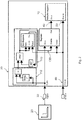
- FIG. 11 shows a view of a first embodiment, having a shadow register 10 in the free-running mode.
- a function with a signal 30 is defined in an FPGA source code 20.
- the signal 30 is assigned to the shadow register 10.
- the shadow register 10 has two inputs 40, 50.
- the shadow register 10 can be switched to active with the enable signal 60.
- the shadow register 10 only accepts the current signal value of the assigned signal 30 in the active state.
- the enable signal 60 can be applied permanently and only interrupted at the desired point in time in order to permanently store the current value in the shadow register.
- the enable signal 60 can only be applied briefly in order to permanently store the current signal value of the signal 30 at the time of the active enable signal in the shadow register.
- the part 70 inserted during the process comprises, in this example, the shadow register 10 and the lines for the signal 30 and the enable signal 60.
- the enable signal 60 is preferably applied externally to the FPGA. However, it is also possible to have the enable signal 60 controlled by the FPGA.
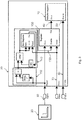
- An intermediate register 100 which can also be regarded as a second shadow register, is connected to the signal 30 and the shadow register 10. Current signal values can be stored in the intermediate register 100 while the shadow register is decoupled.
- a two-part logic circuit 110, 140 is connected to the signal 30 and the intermediate register 100. The first part of the logic circuit 110 detects at runtime that a change in the signal value has taken place. The second part of the logic circuit 140 generates a trigger signal 130, which serves as an enable signal for the second register, when a signal value change is detected by the first part of the logic circuit 110.
- the logic circuit 110, 140 is constructed in such a way that the trigger signal 130 is generated for only one cycle when the signal value changes. As a result, only the first changed signal value is stored in the intermediate register 100.
- the enable signal 60 enables the signal value stored in the intermediate register 100 to be transferred to the shadow register 10. The value can then be read from the shadow register 100, for example via a readback interface.
- the enable signal 60 also serves as a reset signal for the logic circuit 110, 140 and the intermediate register 100.
- the logic circuit 110 140 is designed such that it generates a new trigger signal 130 only after the reset signal has been received. The reset of the intermediate register 100 makes it possible to clearly distinguish in the data read out whether a current value has been read out or only the initialization value of the register after a reset.
- trigger signal 130 can also be forwarded to other inserted circuits.
- a trigger signal can trigger the storage of a large number of signal values. This is beneficial when a consistent set of signal values that are simultaneously present in the FPGA is to be acquired.
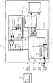
- the part 70 inserted during the method in this example comprises the shadow register 10, the intermediate register 100 and the two-part logic circuit 110, 140.
- the enable signal 60 is not used here as a reset signal for the second register 100 and the two-part logic circuit 110, 140.
- the enable signal 60 is only used to transfer the signal value to the shadow register 10.
- the reset signal 70 for the Logic circuit 110, 140 and the intermediate register 100 are separate from the enable signal 60 and can be controlled from outside or inside the FPGA, depending on the implementation.
- a fourth embodiment is shown. Only the differences to the illustration of the Figure 3 explained.
- a mode switching logic 200 is inserted.
- the mode switching logic 200 receives the reset signal 70, the enable signal 60 and a mode signal 210 as inputs.
- the two-part logic circuit 110, 140 can be overridden, so that the circuit of the fourth embodiment is like the circuit of the first embodiment Figure 1 behaves.
- the enable signal 60 is used as a reset signal for the intermediate register 100 and the two-part logic circuit 110, 140, so that the circuit is like the circuit of the second embodiment Figure 2 behaves. If no mode signal 210 is present, the circuit behaves like the circuit of the third embodiment Figure 3 .
- the fourth embodiment thus represents a combination of the first three embodiments, the behavior can be selected by the mode signal 210 at runtime. This is advantageous if it is not yet clear which behavior is required when the netlist is created.
- FIG. 5 shows a schematic representation of the behavior of the first, second and third embodiment.
- the top line 500 shows an exemplary signal profile of the signal 30. Over time, the signal value changes several times between 0 and 1.
- the second line 510 shows the value of the shadow register 10 using the example of the first exemplary embodiment Figure 1 .
- the enable signal 60 is briefly activated at four different times 550, 560, 570, 580. Since the value of the shadow register is only updated when the enable signal 60 is active, the value of the shadow register 10 remains 0 until the signal value 30 is 1 and the enable signal is active at the same time. The value can then be read from the shadow register.
- the third line 520 shows the value of the intermediate register 100 using the example of the third exemplary embodiment Figure 3 .
- the two-part logic circuit 110, 140 triggers the trigger signal 130 and the current value is transferred to the intermediate register 100.
- the reset signal 70 becomes active at a fifth point in time 590.
- the reset signal 70 sets the value of the intermediate register 100 to 0 and resets the two-part logic circuit 110, 140, so that the next time the signal value of the signal 30 changes, a trigger signal 130 is generated again. Every time the enable signal 60 is active at one of the four indicated times 550, 560, 570, 580, the current value of the intermediate register 100 at these times is transferred to the shadow register 10 and can be read from there.
- the fourth line 530 shows the value of the intermediate register 100 using the example of the second exemplary embodiment Figure 2 .
- the two-part logic circuit 110, 140 triggers the trigger signal 130 and the current value is transferred to the intermediate register 100. Every time the enable signal 60 is active at one of the four indicated times 550, 560, 570, 580, the current value of the intermediate register 100 at these times is transferred to the shadow register 10 and can be read from there.
- the enable signal 60 sets the value of the intermediate register 100 to 0 and resets the two-part logic circuit 110, 140, so that the next time the signal value of the signal 30 changes, a trigger signal 130 is generated again.
- Figure 6 shows a schematic representation of a network list, with preparation for reading out the registers via a readback interface.
- the network list consists of three logic blocks MUX, ADD, MULT and several lines. Two inputs 610, 620 of the network list are fed into two inputs of the first logic block MUX. The output of the first logic block MUX is connected to a first input of the second logic block ADD. A third input 630 of the network list is connected to a second input of the second logic block ADD. The output of the second logic block ADD is connected to a first input of the third logic block MULT.
- a fourth input 640 of the network list is connected to a second input of the third logic block MULT. The output of the third logic block forms the output of the network list.
- Each shadow register REG is assigned to an output signal of a logic block.
- the shadow registers REG are intended and set up for reading out via a readback interface, so no readout logic is added to the network list.
- the shadow registers can be functionally separated from the logic blocks via a decoupling circuit in the same clock step. This means that a consistent data record can be recorded in the shadow registers.
- Figure 7 shows a schematic decoupling circuit with interruption of the clock signal.
- the clock signal 700 of the shadow register is connected to the clock network CLK of the signal assigned to the shadow register via an inserted decoupling mechanism 710.
- the decoupling mechanism can be addressed from inside and / or outside the FPGA at runtime and interrupt the clock signal.
- the signal 30 assigned to the shadow register 10 from the FPGA source code 20 is permanently connected to the signal input 40 of the shadow register 10.
- the shadow register 10 only then takes a current one Signal value when the decoupling mechanism 700 connects the clock signal of the shadow register 10 to the clock network CLK.
- Figure 8 shows a schematic decoupling circuit with interruption of the enable signal.
- the clock signal 700 of the shadow register 10 is connected directly to the clock network CLK in this embodiment.
- a decoupling mechanism is inserted and connected to the enable input 50 of the shadow register 10.
- the decoupling mechanism can be addressed from inside and / or outside the FPGA at runtime and interrupt the enable signal.
- FPGA programs with multiple clock domains can also be operated safely in the ways described above, i.e. without metastable states.
- the shadow register when decoupling with interruption of the clock signal, the shadow register is connected to the clock network with which the assigned signal is also operated.
- the clock lines of the shadow registers are connected to the respective clock network of the assigned signals.
- a separate enable signal with correct clock domain transition is inserted for each clock domain in the FPGA network list and connected to the enable ports of the shadow register of the respective clock domains.
- a clock domain transition can, for example, be correctly exceeded by double registers.
- Figure 9 shows the steps of a method according to the invention. Some steps are mandatory, other steps are optional.
- a copy of the source code is created.
- the minimum required bit widths of the constants in the source code or the copy of the source code are determined.
- the minimum required bit widths determined in the second step S120 are propagated by the source code.
- a signal 30 is determined to which a shadow register 10 is to be assigned. This step can done automatically by an algorithm or by user input.
- a fifth optional step S150 it is checked whether the value of the signal determined in the fourth step S140 can be determined from values of already inserted shadow registers.
- a shadow register 10 is inserted for the signal 30 determined in the fourth step S140.
- a decoupling mechanism is inserted and set up for the shadow register 10, or the shadow register 10 is connected to an already inserted decoupling mechanism. If it was found in the fifth step S150 that the value of the signal 30 determined in the fourth step S140 can be determined from already inserted shadow registers, then in the sixth step S160 no shadow register is inserted, but referenced to the already inserted shadow registers from which the value is derived of the signal can be determined.
- a read-out mechanism is inserted and set up for the shadow register 10 inserted in the sixth step S160.
- Inserting and setting up the read-out mechanism can, for example, consist in inserting an instruction to the implementation tools in the source code, stating that reading via a readback interface should be enabled on the FPGA onto which the netlist is to be loaded.
- the fourth through seventh steps can be repeated several times in order to assign shadow registers to a large number of signals.
- the fourth to seventh steps are preferably processed repeatedly in an automated manner by an algorithm, the algorithm systematically processing all signals defined in the source code.
- a network list is synthesized from the source code. It should be noted that the eighth step S180 can also be carried out before the fourth step S140. In any case, the netlist contains both the information of the original source code and the inserted shadow registers with the set up decoupling mechanism and the set up readout mechanism.
- the network list generated in the eighth step S180 is converted into a bit stream, which is then converted into a optional tenth step S200 can be loaded onto an FPGA and executed there.
- the shadow register 10 inserted in the sixth step S160 can be decoupled from the function of the original source code via the decoupling mechanism and read out via the readout mechanism set up in the seventh step S170.
- the oligatory steps of the method enable the value of the signal 30 determined in the fourth step S140 to be reliably read out during the runtime of the FPGA.
Landscapes
- Engineering & Computer Science (AREA)
- Computer Hardware Design (AREA)
- Physics & Mathematics (AREA)
- Theoretical Computer Science (AREA)
- Evolutionary Computation (AREA)
- Geometry (AREA)
- General Engineering & Computer Science (AREA)
- General Physics & Mathematics (AREA)
- Logic Circuits (AREA)
- Stored Programmes (AREA)
Priority Applications (4)
| Application Number | Priority Date | Filing Date | Title |
|---|---|---|---|
| EP16168899.9A EP3244326B1 (de) | 2016-05-10 | 2016-05-10 | Verfahren zum erstellen einer fpga-netzliste |
| CN201710171544.8A CN107357948B (zh) | 2016-05-10 | 2017-03-22 | 用于建立fpga网表的方法 |
| US15/585,335 US10394989B2 (en) | 2016-05-10 | 2017-05-03 | Method for creating an FPGA netlist |
| JP2017093906A JP6910198B2 (ja) | 2016-05-10 | 2017-05-10 | Fpgaネットリストを作成する方法 |
Applications Claiming Priority (1)
| Application Number | Priority Date | Filing Date | Title |
|---|---|---|---|
| EP16168899.9A EP3244326B1 (de) | 2016-05-10 | 2016-05-10 | Verfahren zum erstellen einer fpga-netzliste |
Publications (2)
| Publication Number | Publication Date |
|---|---|
| EP3244326A1 EP3244326A1 (de) | 2017-11-15 |
| EP3244326B1 true EP3244326B1 (de) | 2021-07-07 |
Family
ID=55967104
Family Applications (1)
| Application Number | Title | Priority Date | Filing Date |
|---|---|---|---|
| EP16168899.9A Active EP3244326B1 (de) | 2016-05-10 | 2016-05-10 | Verfahren zum erstellen einer fpga-netzliste |
Country Status (4)
| Country | Link |
|---|---|
| US (1) | US10394989B2 (enExample) |
| EP (1) | EP3244326B1 (enExample) |
| JP (1) | JP6910198B2 (enExample) |
| CN (1) | CN107357948B (enExample) |
Families Citing this family (6)
| Publication number | Priority date | Publication date | Assignee | Title |
|---|---|---|---|---|
| US10902132B2 (en) | 2017-08-25 | 2021-01-26 | Graf Research Corporation | Private verification for FPGA bitstreams |
| EP3647801A1 (de) | 2018-10-30 | 2020-05-06 | dSPACE digital signal processing and control engineering GmbH | Verfahren zur überprüfung eines fpga-programms |
| CN109739705A (zh) * | 2018-12-29 | 2019-05-10 | 西安智多晶微电子有限公司 | 一种fpga片上实时调试系统及方法 |
| US11216277B2 (en) * | 2019-09-26 | 2022-01-04 | Arm Limited | Apparatus and method of capturing a register state |
| DE102021133835A1 (de) * | 2021-12-20 | 2023-06-22 | Dspace Gmbh | Verfahren und Anordnung zur partiellen Neuprogrammierung einer programmierbaren Gatteranordnung |
| DE102023100161A1 (de) | 2023-01-04 | 2024-07-04 | Dspace Gmbh | Überwachungsschaltung für eine programmierbare gatteranordnung, anordnung mit überwachungsschaltung, prozessor und gatteranordnung sowie verfahren zum betrieb einer solchen anordnung |
Family Cites Families (11)
| Publication number | Priority date | Publication date | Assignee | Title |
|---|---|---|---|---|
| US5764079A (en) * | 1996-03-11 | 1998-06-09 | Altera Corporation | Sample and load scheme for observability of internal nodes in a PLD |
| GB2318664B (en) * | 1996-10-28 | 2000-08-23 | Altera Corp | Embedded logic analyzer for a programmable logic device |
| DE10196175T1 (de) * | 2000-05-11 | 2003-04-17 | Quickturn Design Systems Inc | Emulations-Schaltkreis mit einem Haltezeit-Algorithmus, Logikanalysierer und Shadow-Speicher |
| US7213216B2 (en) * | 2002-08-09 | 2007-05-01 | Synplicity, Inc. | Method and system for debugging using replicated logic and trigger logic |
| US8781808B2 (en) * | 2005-10-10 | 2014-07-15 | Sei Yang Yang | Prediction-based distributed parallel simulation method |
| CN101933098A (zh) * | 2007-09-18 | 2010-12-29 | 明导公司 | 使用线性反馈移位寄存器在存储器内建自测试环境中的故障诊断 |
| US9262303B2 (en) * | 2008-12-05 | 2016-02-16 | Altera Corporation | Automated semiconductor design flaw detection system |
| US9576092B2 (en) * | 2009-02-24 | 2017-02-21 | Mentor Graphics Corporation | Synthesis using multiple synthesis engine configurations |
| US8972923B2 (en) * | 2011-02-08 | 2015-03-03 | Maxeler Technologies Ltd. | Method and apparatus and software code for generating a hardware stream processor design |
| EP2765528B1 (de) | 2013-02-11 | 2018-11-14 | dSPACE digital signal processing and control engineering GmbH | Wahlfreier Zugriff auf Signalwerte eines FPGA zur Laufzeit |
| JP6436916B2 (ja) * | 2013-02-11 | 2018-12-12 | ディスペース デジタル シグナル プロセッシング アンド コントロール エンジニアリング ゲゼルシャフト ミット ベシュレンクテル ハフツングdspace digital signal processing and control engineering GmbH | ランタイムにfpgaの信号値を変更するための方法、当該方法を実施するためのデータ処理装置、コンピュータプログラムおよびディジタル記憶媒体 |
-
2016
- 2016-05-10 EP EP16168899.9A patent/EP3244326B1/de active Active
-
2017
- 2017-03-22 CN CN201710171544.8A patent/CN107357948B/zh active Active
- 2017-05-03 US US15/585,335 patent/US10394989B2/en active Active
- 2017-05-10 JP JP2017093906A patent/JP6910198B2/ja active Active
Also Published As
| Publication number | Publication date |
|---|---|
| US20170329877A1 (en) | 2017-11-16 |
| US10394989B2 (en) | 2019-08-27 |
| JP6910198B2 (ja) | 2021-07-28 |
| JP2017204279A (ja) | 2017-11-16 |
| EP3244326A1 (de) | 2017-11-15 |
| CN107357948A (zh) | 2017-11-17 |
| CN107357948B (zh) | 2023-04-07 |
Similar Documents
| Publication | Publication Date | Title |
|---|---|---|
| EP3244326B1 (de) | Verfahren zum erstellen einer fpga-netzliste | |
| EP2765528B1 (de) | Wahlfreier Zugriff auf Signalwerte eines FPGA zur Laufzeit | |
| EP2954440B1 (de) | Verändern eines signalwerts eines fpga zur laufzeit | |
| DE69225527T2 (de) | Verfahren und System zur automatischen Bestimmung der logischen Funktion einer Schaltung | |
| EP2799983B1 (de) | Flexible Aufteilung der I/O Kanäle einer Hardware Komponente | |
| DE102019003851A1 (de) | Systeme und Verfahren zum automatischen Realisieren von Modellen zu Co-Simulation | |
| DE10143101A1 (de) | Verfahren zur Validierung von Simulationsergebnissen eines Systems sowie darauf aufbauender Äquivalenzvergleich digitaler Schaltungen | |
| DE112020006021T5 (de) | Auf maschinelles lernen basierendes verfahren und vorrichtung für die berechnung und verifizierung von verzögerungen des entwurfs integrierter schaltungen | |
| EP2963541B1 (de) | Implementierung einer Konstanten in FPGA-Code | |
| DE102013101300A1 (de) | Wahlfreier Zugriff auf Signalwerte eines FPGA zur Laufzeit | |
| EP4068138A1 (de) | Verfahren zur aufteilung von simulationsmodellen zwischen einem prozessor und einem fpga | |
| EP2899652B1 (de) | Verfahren zur Einsatzoptimierung programmierbarer Logikbausteine in Steuerungsgeräten für Fahrzeuge | |
| DE102008007004B4 (de) | Integrierte Schaltung mit einem Speicher mit mehreren Speicherzellen mit synchronem Aufbau, die mit Taktausblendeeinheiten verbunden sind, sowie Verfahren zum Entwerfen einer solchen Schaltung | |
| EP3142032B1 (de) | Verfahren zum ändern der konfiguration eines programmierbaren logikbausteins | |
| WO2011134762A1 (de) | Coprozessor mit aufgabenablaufsteuerung | |
| EP3455751B1 (de) | Verfahren zum bestimmen von signalwerten aus einem fpga zur laufzeit | |
| EP3001318A1 (de) | Bestimmung von Signalen für Readback aus FPGA | |
| DE102015104460B4 (de) | Priorisieren von ereignissen, auf die ein prozessor reagieren soll | |
| DE10325513B4 (de) | Verfahren und Vorrichtung zum Erstellen eines Verhaltensaspekts einer Schaltung zur formalen Verifikation | |
| EP3739479B1 (de) | Verfahren zur fehlersuche in der programmlogik eines systems verteilter programmierbarer gatteranordnungen | |
| DE69132766T2 (de) | Gatter-Adressierungssystem für eine Logiksimulationsmaschine | |
| EP0828215B1 (de) | Verfahren zur Verifikation eines Programms, welches in einer Sprache für speicher-programmierbare Steuerungen vorliegt, durch einen Rechner | |
| DE102017126094A1 (de) | Verfahren zum Auslesen von Variablen aus einem FPGA | |
| AT501880B1 (de) | Speicherprogrammierbare steuerung | |
| EP3242232A1 (de) | Optimierte erzeugung von gesamtnetzliste und bitstrom |
Legal Events
| Date | Code | Title | Description |
|---|---|---|---|
| PUAI | Public reference made under article 153(3) epc to a published international application that has entered the european phase |
Free format text: ORIGINAL CODE: 0009012 |
|
| STAA | Information on the status of an ep patent application or granted ep patent |
Free format text: STATUS: THE APPLICATION HAS BEEN PUBLISHED |
|
| AK | Designated contracting states |
Kind code of ref document: A1 Designated state(s): AL AT BE BG CH CY CZ DE DK EE ES FI FR GB GR HR HU IE IS IT LI LT LU LV MC MK MT NL NO PL PT RO RS SE SI SK SM TR |
|
| AX | Request for extension of the european patent |
Extension state: BA ME |
|
| STAA | Information on the status of an ep patent application or granted ep patent |
Free format text: STATUS: REQUEST FOR EXAMINATION WAS MADE |
|
| 17P | Request for examination filed |
Effective date: 20180515 |
|
| RBV | Designated contracting states (corrected) |
Designated state(s): AL AT BE BG CH CY CZ DE DK EE ES FI FR GB GR HR HU IE IS IT LI LT LU LV MC MK MT NL NO PL PT RO RS SE SI SK SM TR |
|
| REG | Reference to a national code |
Ref country code: DE Ref legal event code: R079 Ref document number: 502016013347 Country of ref document: DE Free format text: PREVIOUS MAIN CLASS: G06F0017500000 Ipc: G06F0030331000 |
|
| GRAP | Despatch of communication of intention to grant a patent |
Free format text: ORIGINAL CODE: EPIDOSNIGR1 |
|
| STAA | Information on the status of an ep patent application or granted ep patent |
Free format text: STATUS: GRANT OF PATENT IS INTENDED |
|
| RIC1 | Information provided on ipc code assigned before grant |
Ipc: G06F 30/331 20200101AFI20210226BHEP Ipc: G06F 30/34 20200101ALI20210226BHEP |
|
| INTG | Intention to grant announced |
Effective date: 20210324 |
|
| GRAS | Grant fee paid |
Free format text: ORIGINAL CODE: EPIDOSNIGR3 |
|
| GRAA | (expected) grant |
Free format text: ORIGINAL CODE: 0009210 |
|
| STAA | Information on the status of an ep patent application or granted ep patent |
Free format text: STATUS: THE PATENT HAS BEEN GRANTED |
|
| AK | Designated contracting states |
Kind code of ref document: B1 Designated state(s): AL AT BE BG CH CY CZ DE DK EE ES FI FR GB GR HR HU IE IS IT LI LT LU LV MC MK MT NL NO PL PT RO RS SE SI SK SM TR |
|
| REG | Reference to a national code |
Ref country code: GB Ref legal event code: FG4D Free format text: NOT ENGLISH |
|
| REG | Reference to a national code |
Ref country code: AT Ref legal event code: REF Ref document number: 1409290 Country of ref document: AT Kind code of ref document: T Effective date: 20210715 |
|
| REG | Reference to a national code |
Ref country code: DE Ref legal event code: R096 Ref document number: 502016013347 Country of ref document: DE |
|
| REG | Reference to a national code |
Ref country code: IE Ref legal event code: FG4D Free format text: LANGUAGE OF EP DOCUMENT: GERMAN |
|
| REG | Reference to a national code |
Ref country code: LT Ref legal event code: MG9D |
|
| REG | Reference to a national code |
Ref country code: NL Ref legal event code: MP Effective date: 20210707 |
|
| REG | Reference to a national code |
Ref country code: DE Ref legal event code: R081 Ref document number: 502016013347 Country of ref document: DE Owner name: DSPACE GMBH, DE Free format text: FORMER OWNER: DSPACE DIGITAL SIGNAL PROCESSING AND CONTROL ENGINEERING GMBH, 33102 PADERBORN, DE |
|
| RAP4 | Party data changed (patent owner data changed or rights of a patent transferred) |
Owner name: DSPACE GMBH |
|
| PG25 | Lapsed in a contracting state [announced via postgrant information from national office to epo] |
Ref country code: BG Free format text: LAPSE BECAUSE OF FAILURE TO SUBMIT A TRANSLATION OF THE DESCRIPTION OR TO PAY THE FEE WITHIN THE PRESCRIBED TIME-LIMIT Effective date: 20211007 Ref country code: LT Free format text: LAPSE BECAUSE OF FAILURE TO SUBMIT A TRANSLATION OF THE DESCRIPTION OR TO PAY THE FEE WITHIN THE PRESCRIBED TIME-LIMIT Effective date: 20210707 Ref country code: FI Free format text: LAPSE BECAUSE OF FAILURE TO SUBMIT A TRANSLATION OF THE DESCRIPTION OR TO PAY THE FEE WITHIN THE PRESCRIBED TIME-LIMIT Effective date: 20210707 Ref country code: ES Free format text: LAPSE BECAUSE OF FAILURE TO SUBMIT A TRANSLATION OF THE DESCRIPTION OR TO PAY THE FEE WITHIN THE PRESCRIBED TIME-LIMIT Effective date: 20210707 Ref country code: NO Free format text: LAPSE BECAUSE OF FAILURE TO SUBMIT A TRANSLATION OF THE DESCRIPTION OR TO PAY THE FEE WITHIN THE PRESCRIBED TIME-LIMIT Effective date: 20211007 Ref country code: NL Free format text: LAPSE BECAUSE OF FAILURE TO SUBMIT A TRANSLATION OF THE DESCRIPTION OR TO PAY THE FEE WITHIN THE PRESCRIBED TIME-LIMIT Effective date: 20210707 Ref country code: PT Free format text: LAPSE BECAUSE OF FAILURE TO SUBMIT A TRANSLATION OF THE DESCRIPTION OR TO PAY THE FEE WITHIN THE PRESCRIBED TIME-LIMIT Effective date: 20211108 Ref country code: HR Free format text: LAPSE BECAUSE OF FAILURE TO SUBMIT A TRANSLATION OF THE DESCRIPTION OR TO PAY THE FEE WITHIN THE PRESCRIBED TIME-LIMIT Effective date: 20210707 Ref country code: RS Free format text: LAPSE BECAUSE OF FAILURE TO SUBMIT A TRANSLATION OF THE DESCRIPTION OR TO PAY THE FEE WITHIN THE PRESCRIBED TIME-LIMIT Effective date: 20210707 Ref country code: SE Free format text: LAPSE BECAUSE OF FAILURE TO SUBMIT A TRANSLATION OF THE DESCRIPTION OR TO PAY THE FEE WITHIN THE PRESCRIBED TIME-LIMIT Effective date: 20210707 |
|
| PG25 | Lapsed in a contracting state [announced via postgrant information from national office to epo] |
Ref country code: PL Free format text: LAPSE BECAUSE OF FAILURE TO SUBMIT A TRANSLATION OF THE DESCRIPTION OR TO PAY THE FEE WITHIN THE PRESCRIBED TIME-LIMIT Effective date: 20210707 Ref country code: LV Free format text: LAPSE BECAUSE OF FAILURE TO SUBMIT A TRANSLATION OF THE DESCRIPTION OR TO PAY THE FEE WITHIN THE PRESCRIBED TIME-LIMIT Effective date: 20210707 Ref country code: GR Free format text: LAPSE BECAUSE OF FAILURE TO SUBMIT A TRANSLATION OF THE DESCRIPTION OR TO PAY THE FEE WITHIN THE PRESCRIBED TIME-LIMIT Effective date: 20211008 |
|
| REG | Reference to a national code |
Ref country code: DE Ref legal event code: R097 Ref document number: 502016013347 Country of ref document: DE |
|
| PG25 | Lapsed in a contracting state [announced via postgrant information from national office to epo] |
Ref country code: DK Free format text: LAPSE BECAUSE OF FAILURE TO SUBMIT A TRANSLATION OF THE DESCRIPTION OR TO PAY THE FEE WITHIN THE PRESCRIBED TIME-LIMIT Effective date: 20210707 |
|
| PLBE | No opposition filed within time limit |
Free format text: ORIGINAL CODE: 0009261 |
|
| STAA | Information on the status of an ep patent application or granted ep patent |
Free format text: STATUS: NO OPPOSITION FILED WITHIN TIME LIMIT |
|
| PG25 | Lapsed in a contracting state [announced via postgrant information from national office to epo] |
Ref country code: SM Free format text: LAPSE BECAUSE OF FAILURE TO SUBMIT A TRANSLATION OF THE DESCRIPTION OR TO PAY THE FEE WITHIN THE PRESCRIBED TIME-LIMIT Effective date: 20210707 Ref country code: SK Free format text: LAPSE BECAUSE OF FAILURE TO SUBMIT A TRANSLATION OF THE DESCRIPTION OR TO PAY THE FEE WITHIN THE PRESCRIBED TIME-LIMIT Effective date: 20210707 Ref country code: RO Free format text: LAPSE BECAUSE OF FAILURE TO SUBMIT A TRANSLATION OF THE DESCRIPTION OR TO PAY THE FEE WITHIN THE PRESCRIBED TIME-LIMIT Effective date: 20210707 Ref country code: EE Free format text: LAPSE BECAUSE OF FAILURE TO SUBMIT A TRANSLATION OF THE DESCRIPTION OR TO PAY THE FEE WITHIN THE PRESCRIBED TIME-LIMIT Effective date: 20210707 Ref country code: CZ Free format text: LAPSE BECAUSE OF FAILURE TO SUBMIT A TRANSLATION OF THE DESCRIPTION OR TO PAY THE FEE WITHIN THE PRESCRIBED TIME-LIMIT Effective date: 20210707 Ref country code: AL Free format text: LAPSE BECAUSE OF FAILURE TO SUBMIT A TRANSLATION OF THE DESCRIPTION OR TO PAY THE FEE WITHIN THE PRESCRIBED TIME-LIMIT Effective date: 20210707 |
|
| 26N | No opposition filed |
Effective date: 20220408 |
|
| PG25 | Lapsed in a contracting state [announced via postgrant information from national office to epo] |
Ref country code: IT Free format text: LAPSE BECAUSE OF FAILURE TO SUBMIT A TRANSLATION OF THE DESCRIPTION OR TO PAY THE FEE WITHIN THE PRESCRIBED TIME-LIMIT Effective date: 20210707 |
|
| REG | Reference to a national code |
Ref country code: CH Ref legal event code: PL |
|
| REG | Reference to a national code |
Ref country code: BE Ref legal event code: MM Effective date: 20220531 |
|
| GBPC | Gb: european patent ceased through non-payment of renewal fee |
Effective date: 20220510 |
|
| PG25 | Lapsed in a contracting state [announced via postgrant information from national office to epo] |
Ref country code: MC Free format text: LAPSE BECAUSE OF FAILURE TO SUBMIT A TRANSLATION OF THE DESCRIPTION OR TO PAY THE FEE WITHIN THE PRESCRIBED TIME-LIMIT Effective date: 20210707 Ref country code: LU Free format text: LAPSE BECAUSE OF NON-PAYMENT OF DUE FEES Effective date: 20220510 Ref country code: LI Free format text: LAPSE BECAUSE OF NON-PAYMENT OF DUE FEES Effective date: 20220531 Ref country code: CH Free format text: LAPSE BECAUSE OF NON-PAYMENT OF DUE FEES Effective date: 20220531 |
|
| PG25 | Lapsed in a contracting state [announced via postgrant information from national office to epo] |
Ref country code: IE Free format text: LAPSE BECAUSE OF NON-PAYMENT OF DUE FEES Effective date: 20220510 Ref country code: FR Free format text: LAPSE BECAUSE OF NON-PAYMENT OF DUE FEES Effective date: 20220531 |
|
| PG25 | Lapsed in a contracting state [announced via postgrant information from national office to epo] |
Ref country code: GB Free format text: LAPSE BECAUSE OF NON-PAYMENT OF DUE FEES Effective date: 20220510 Ref country code: BE Free format text: LAPSE BECAUSE OF NON-PAYMENT OF DUE FEES Effective date: 20220531 |
|
| P01 | Opt-out of the competence of the unified patent court (upc) registered |
Effective date: 20230525 |
|
| REG | Reference to a national code |
Ref country code: AT Ref legal event code: MM01 Ref document number: 1409290 Country of ref document: AT Kind code of ref document: T Effective date: 20220510 |
|
| PG25 | Lapsed in a contracting state [announced via postgrant information from national office to epo] |
Ref country code: AT Free format text: LAPSE BECAUSE OF NON-PAYMENT OF DUE FEES Effective date: 20220510 |
|
| PG25 | Lapsed in a contracting state [announced via postgrant information from national office to epo] |
Ref country code: HU Free format text: LAPSE BECAUSE OF FAILURE TO SUBMIT A TRANSLATION OF THE DESCRIPTION OR TO PAY THE FEE WITHIN THE PRESCRIBED TIME-LIMIT; INVALID AB INITIO Effective date: 20160510 |
|
| PG25 | Lapsed in a contracting state [announced via postgrant information from national office to epo] |
Ref country code: MK Free format text: LAPSE BECAUSE OF FAILURE TO SUBMIT A TRANSLATION OF THE DESCRIPTION OR TO PAY THE FEE WITHIN THE PRESCRIBED TIME-LIMIT Effective date: 20210707 Ref country code: CY Free format text: LAPSE BECAUSE OF FAILURE TO SUBMIT A TRANSLATION OF THE DESCRIPTION OR TO PAY THE FEE WITHIN THE PRESCRIBED TIME-LIMIT Effective date: 20210707 |
|
| PG25 | Lapsed in a contracting state [announced via postgrant information from national office to epo] |
Ref country code: MT Free format text: LAPSE BECAUSE OF FAILURE TO SUBMIT A TRANSLATION OF THE DESCRIPTION OR TO PAY THE FEE WITHIN THE PRESCRIBED TIME-LIMIT Effective date: 20210707 |
|
| PGFP | Annual fee paid to national office [announced via postgrant information from national office to epo] |
Ref country code: DE Payment date: 20250521 Year of fee payment: 10 |
|
| PG25 | Lapsed in a contracting state [announced via postgrant information from national office to epo] |
Ref country code: TR Free format text: LAPSE BECAUSE OF FAILURE TO SUBMIT A TRANSLATION OF THE DESCRIPTION OR TO PAY THE FEE WITHIN THE PRESCRIBED TIME-LIMIT Effective date: 20210707 |