EP3244326B1 - Method for creating a fpga netlist - Google Patents
Method for creating a fpga netlist Download PDFInfo
- Publication number
- EP3244326B1 EP3244326B1 EP16168899.9A EP16168899A EP3244326B1 EP 3244326 B1 EP3244326 B1 EP 3244326B1 EP 16168899 A EP16168899 A EP 16168899A EP 3244326 B1 EP3244326 B1 EP 3244326B1
- Authority
- EP
- European Patent Office
- Prior art keywords
- signal
- fpga
- shadow register
- shadow
- source code
- Prior art date
- Legal status (The legal status is an assumption and is not a legal conclusion. Google has not performed a legal analysis and makes no representation as to the accuracy of the status listed.)
- Active
Links
- 238000000034 method Methods 0.000 title claims description 35
- 238000012545 processing Methods 0.000 claims description 11
- 238000005457 optimization Methods 0.000 claims description 5
- 238000005266 casting Methods 0.000 claims description 3
- 230000001902 propagating effect Effects 0.000 claims 1
- 230000007246 mechanism Effects 0.000 description 16
- 230000006870 function Effects 0.000 description 15
- 238000004088 simulation Methods 0.000 description 9
- 238000010586 diagram Methods 0.000 description 5
- 230000006399 behavior Effects 0.000 description 4
- 238000004422 calculation algorithm Methods 0.000 description 3
- 230000008859 change Effects 0.000 description 3
- 230000008569 process Effects 0.000 description 3
- 230000004044 response Effects 0.000 description 3
- 238000003860 storage Methods 0.000 description 3
- 238000012360 testing method Methods 0.000 description 3
- 230000008901 benefit Effects 0.000 description 2
- 230000015572 biosynthetic process Effects 0.000 description 2
- 238000002360 preparation method Methods 0.000 description 2
- 230000001360 synchronised effect Effects 0.000 description 2
- 238000003786 synthesis reaction Methods 0.000 description 2
- 230000007704 transition Effects 0.000 description 2
- 230000001960 triggered effect Effects 0.000 description 2
- 238000003491 array Methods 0.000 description 1
- 230000009286 beneficial effect Effects 0.000 description 1
- 238000004364 calculation method Methods 0.000 description 1
- 238000004590 computer program Methods 0.000 description 1
- 230000001419 dependent effect Effects 0.000 description 1
- 238000011161 development Methods 0.000 description 1
- 238000003780 insertion Methods 0.000 description 1
- 230000037431 insertion Effects 0.000 description 1
- 238000013507 mapping Methods 0.000 description 1
- 230000000644 propagated effect Effects 0.000 description 1
- 230000000717 retained effect Effects 0.000 description 1
- 238000012546 transfer Methods 0.000 description 1
Images


Classifications
-
- G—PHYSICS
- G06—COMPUTING; CALCULATING OR COUNTING
- G06F—ELECTRIC DIGITAL DATA PROCESSING
- G06F30/00—Computer-aided design [CAD]
- G06F30/30—Circuit design
- G06F30/34—Circuit design for reconfigurable circuits, e.g. field programmable gate arrays [FPGA] or programmable logic devices [PLD]
- G06F30/343—Logical level
-
- G—PHYSICS
- G06—COMPUTING; CALCULATING OR COUNTING
- G06F—ELECTRIC DIGITAL DATA PROCESSING
- G06F30/00—Computer-aided design [CAD]
- G06F30/30—Circuit design
- G06F30/34—Circuit design for reconfigurable circuits, e.g. field programmable gate arrays [FPGA] or programmable logic devices [PLD]
-
- G—PHYSICS
- G06—COMPUTING; CALCULATING OR COUNTING
- G06F—ELECTRIC DIGITAL DATA PROCESSING
- G06F30/00—Computer-aided design [CAD]
- G06F30/30—Circuit design
- G06F30/32—Circuit design at the digital level
- G06F30/327—Logic synthesis; Behaviour synthesis, e.g. mapping logic, HDL to netlist, high-level language to RTL or netlist
-
- G—PHYSICS
- G06—COMPUTING; CALCULATING OR COUNTING
- G06F—ELECTRIC DIGITAL DATA PROCESSING
- G06F30/00—Computer-aided design [CAD]
- G06F30/30—Circuit design
- G06F30/32—Circuit design at the digital level
- G06F30/33—Design verification, e.g. functional simulation or model checking
-
- G—PHYSICS
- G06—COMPUTING; CALCULATING OR COUNTING
- G06F—ELECTRIC DIGITAL DATA PROCESSING
- G06F30/00—Computer-aided design [CAD]
- G06F30/30—Circuit design
- G06F30/32—Circuit design at the digital level
- G06F30/33—Design verification, e.g. functional simulation or model checking
- G06F30/3308—Design verification, e.g. functional simulation or model checking using simulation
- G06F30/331—Design verification, e.g. functional simulation or model checking using simulation with hardware acceleration, e.g. by using field programmable gate array [FPGA] or emulation
Definitions
- the present invention relates to a method for creating a network list for an FPGA.
- Field Programmable Gate Arrays can support computing nodes in real-time simulation by taking over the calculation of dynamic parts of a model. Due to the high flexibility and the possibility of parallel processing of signals, even hard real-time requirements can easily be met through the use of FPGAs.
- the FPGAs can serve as hardware accelerators for CPUs of computing nodes. Accordingly, very dynamic parts of the environment model, for example, are outsourced to the FPGA, so that sufficiently precise and fast response times for the control unit are guaranteed.
- An FPGA network list is usually generated in a build process based on an FPGA model in a hardware description language.
- An FPGA-based simulation can be modeled in a block diagram with Simulink using the Xilinx System Generator (XSG) and the FPGA programming block set from dSPACE, analogous to the CPU-based simulation.
- XSG Xilinx System Generator
- dSPACE dSPACE
- this model is not translated into an iterative programming language, but into an FPGA network list that describes a customer-specific digital circuit.
- the FPGA netlist can be translated into an FPGA configuration data stream.
- HUTCHINGS BRAD LET AL "Rapid Post-Map Insertion of Embedded Logic Analyzers for Xilinx FPGAs" describes the use of BlockRAM as a TraceBuffer.
- US 2010/146338 A1 describes a system for comparing an FPGA with an HDL simulation.
- the data is read out directly from the working registers.
- this is disadvantageous because it is often not possible to read out a register at a specific point in time. Since the working registers are constantly overwritten with current values during runtime, a value that is available at a specific point in time often cannot be recorded.
- the object of the invention is to develop the state of the art.
- the invention relates to a method for creating an FPGA network list, the network list being generated from an FPGA source code and at least one shadow register, wherein the FPGA source code defines at least one function and at least one signal, wherein the shadow register is assigned to the at least one signal and is set up and provided to store the value of the assigned signal at runtime, a possibility for reading out the stored signal value at runtime is provided and set up, where the function defined in the FPGA source code is through the shadow register is not changed,
- the netlist is intended to be loaded onto an FPGA and executed by the FPGA, where the function described by the FPGA source code is carried out by the FPGA, a functional decoupling of the shadow register from the function described in the FPGA source code is provided and set up, whereby the shadow register retains the signal value stored at the time of the uncoupling due to the decoupling, while the function described in the FPGA source code is carried out.
- a data processing device with a processor unit is also specified, the data processing device being designed to carry out the above method.
- a computer program product with computer-implemented instructions is also specified which, after loading and execution in a suitable data processing device, executes the steps of the above method.
- a digital storage medium with electronically readable control signals is specified which can interact with a programmable data processing device in such a way that the above method is carried out on the data processing device.
- the netlist can be converted into a bit stream and loaded onto an FPGA.
- the FPGA can then perform the function defined in the FPGA source code.
- the decoupling makes it possible to read out exactly the value that was current at the time of the decoupling, even if the signal values are read out with a delay.
- the function defined in the FPGA source code continues to be executed and the signal value continues to be updated during which the shadow register is decoupled and that at the time of Uncoupling maintains current value.
- the decoupling is preferably triggered by a trigger signal.
- the decoupling mechanism is linked to the trigger signal in the FPGA network list.
- the shadow register can be decoupled by default and briefly connected to the function in response to a trigger signal. The current signal value at the time of the trigger signal is then stored in the shadow register and the shadow register is decoupled from the function again.
- the result of the method according to the invention is consequently an FPGA network list, with at least one shadow register being defined in the network list, with at least one function and at least one signal being defined in the FPGA network list, with the shadow register being connected to the at least one signal and in addition
- the value of the signal is set up and intended to be stored at runtime, the netlist being loaded onto an FPGA and executed by the FPGA, with the possibility of reading out the signal value stored in the shadow register at runtime of the FPGA in the netlist and is set up, wherein a functional decoupling of the shadow register from the signal is provided and set up, the shadow register retaining the signal value stored at the time of the decoupling as a result of the decoupling while the FPGA is executing the function.
- the FPGA source code defines a multiplicity of signals, a multiplicity of shadow registers being assigned to one signal in each case, the functional decoupling being provided for synchronously decoupling the multiplicity of shadow registers.
- the synchronous decoupling makes it possible to read out a large number of signal values present at the same time from the FPGA during runtime.
- the synchronous reading of several signal values from an FPGA is often not possible.
- the synchronously decoupled shadow register allows signal values present at the same time to be saved and read out one after the other. In this way, a consistent data set of simultaneously available variables can be retained.
- the result of the preferred embodiment is an FPGA network list, a plurality of signals being defined in the FPGA network list, a plurality of shadow registers being assigned to one signal, the functional decoupling being provided to decouple the plurality of shadow registers synchronously.
- the enable signal of the shadow register or the clock signal of the shadow register is interrupted for decoupling.
- the shadow register Due to the interruption of the enable signal of the shadow register, the shadow register is no longer updated during runtime. This is a very simple way of decoupling one or more shadow registers.
- the shadow register no longer accepts any changes, so that the state of the register is more or less frozen.
- the value stored in the shadow register can still be read out in various ways.
- the result of the preferred refinement is an FPGA network list, the network list providing to interrupt the enable signal of the shadow register or the clock signal of the shadow register for decoupling.
- the FPGA source code is available as a graphic model or as textual code.
- FPGA source code is often in the form of a graphical model, such as a block diagram in a development environment. Examples of such block diagrams is Simulink from The MathWorks.
- shadow registers can easily be inserted as additional registers, whereby the additional registers are connected to the assigned signal and can be functionally decoupled from the signal during runtime using a decoupling mechanism that has also been inserted.
- FPGA source code is textual code, for example VHDL or Verilog. Shadow registers can also be easily inserted as additional registers in textual source code, whereby the additional registers are connected to the assigned signal and can be functionally decoupled from the signal at runtime using a decoupling mechanism that has also been inserted.
- the shadow register is inserted into the FPGA source code or a copy of the FPGA source code is inserted.
- a network list is generated from the source code and the shadow register is inserted into the network list.
- the FPGA source code remains unchanged without having to make a copy.
- the netlist with the shadow registers can then be used like any other netlist. For example, it can be converted into a bit stream and then loaded onto an FPGA.
- the network list into which the shadow register is inserted can be present as a simple network list or with additional information about mapping, placing and / or routing.
- the shadow register is automatically inserted and assigned to the signal.
- the automation relieves the user of the task of inserting the shadow register and assigning it to the signal. Automation is of great advantage, especially when there are a large number of signals, each of which is to be assigned a shadow register.
- an automated check is carried out to determine whether the signal is already assigned to a shadow register elsewhere and then no further shadow register is assigned to this signal.
- the automated test prevents a large number of shadow registers from being inserted and assigned to the signal for a signal.
- the FPGA source code is large, that is to say comprises many lines of text or comprises a large number of hierarchical levels as a graphic model, manual testing is time-consuming and error-prone, and automated testing is therefore advantageous.
- At least two shadow registers are inserted and assigned to the signal, the first shadow register being provided and set up to store a current signal value at runtime, while the second shadow register is decoupled.
- Shadow registers With two shadow registers it is possible to hold an old signal value in the first shadow register and at the same time record a current signal value in the second shadow register. This can be used, for example, if the readout process of the shadow register takes several FPGA cycles or cannot be carried out immediately. A current value can then be stored in the second shadow register while the first shadow register is being read out.
- Shadow registers can also represent a memory window.
- a current signal value is stored in one shadow register and an old signal value is stored in the other shadow register.
- the shadow registers can be decoupled at the same time in response to a trigger signal. This makes it possible to read out the signal value before the trigger signal.
- a memory window can be used to hold a signal value following a trigger signal.
- the shadow registers are disconnected one after the other after a predetermined period of time. With three or more shadow registers, both variants can be used at the same time. This makes it possible to record and read out the signal value before and after a trigger signal.
- the result of the preferred refinement is an FPGA network list, at least two shadow registers being defined in the FPGA network list and being assigned to one signal, the first shadow register being provided and set up to store a current signal value at runtime, while the second shadow register is disconnected.
- reading out the shadow register via an external and / or internal readback interface of the FPGA is provided and set up.
- Reading out the shadow register via an internal or external readback interface is a convenient way of reading out.
- very little logic and routing resources of the FPGA are required for reading out.
- the shadow register can be placed directly next to the assigned signal using the implementation tools. As a result, the change compared to a network list without an inserted shadow register is minimal.
- a plurality of shadow registers is inserted, the plurality of shadow registers becoming one Shift register chain are connected and provided and set up to be read out via an external interface of the FPGA.
- a large number of shadow registers are inserted, an address decoder being provided and set up for reading out the large number of shadow registers via an external interface of the FPGA.
- Reading out via an external interface typically enables a higher data throughput than a readback interface. This form of reading is therefore advantageous if a large number of signal values are often to be read out during runtime.
- a logic is inserted in addition to the shadow register, the logic being provided and set up to output a trigger signal at runtime when the signal value changes, the trigger signal causing the shadow register to be decoupled.
- the decoupling can be triggered very quickly when predetermined events occur.
- the trigger signal can then trigger the uncoupling of one or more shadow registers immediately or with a predetermined delay.
- Such logic can be implemented in a number of ways. Examples of this can be found in the exemplary embodiments.
- Constant blocks in graphic FPGA models or VHDL signals in VHDL models are often instantiated with a fixed bit width (e.g. 32 bits). When subsequently specifying the values, however, values are usually used that do not exhaust the value range of the specified bit width.
- the VHDL code generated from the graphic model also contains the full bit widths, regardless of the bit widths actually required. The manual programming of VHDL code is usually done in the same way.
- the inserted shadow registers which are set up for reading out via an external interface, are not optimized by the synthesis and implementation tools, since these tools do not optimize external access. In order to keep the resource consumption by the inserted shadow registers and the readout logic low, it is therefore advantageous to determine the minimum required bit width of the constants and of all signals dependent on the constants. The shadow register can then be implemented in the minimum required bit width of the assigned signal.
- the shadow register is protected from route optimization during the creation and / or further processing of the network list.
- Registers that have no outputs are generally optimized away, ie deleted, by the automated tools that are used for creating and further processing the network list. This is generally useful, as these registers would otherwise be resources in the FPGA prove without contributing to its function.
- the shadow registers inserted in the method according to the invention which are to be read out via a readback interface, have no outputs and would therefore be deleted by the tools.
- the shadow registers are required in order to be able to read the signal values from the FPGA during runtime. It is therefore advantageous to protect the shadow registers from route optimization.
- One possibility to achieve this is to add attributes to the shadow registers and the signals contained therein, the attributes being recognized by the tools and the tools not causing any optimization measures to be carried out on the registers.
- a combination of the shadow registers protected from route optimization with the above-mentioned steps for determining the minimum required bit width is particularly advantageous.
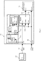
- FIG. 11 shows a view of a first embodiment, having a shadow register 10 in the free-running mode.
- a function with a signal 30 is defined in an FPGA source code 20.
- the signal 30 is assigned to the shadow register 10.
- the shadow register 10 has two inputs 40, 50.
- the shadow register 10 can be switched to active with the enable signal 60.
- the shadow register 10 only accepts the current signal value of the assigned signal 30 in the active state.
- the enable signal 60 can be applied permanently and only interrupted at the desired point in time in order to permanently store the current value in the shadow register.
- the enable signal 60 can only be applied briefly in order to permanently store the current signal value of the signal 30 at the time of the active enable signal in the shadow register.
- the part 70 inserted during the process comprises, in this example, the shadow register 10 and the lines for the signal 30 and the enable signal 60.
- the enable signal 60 is preferably applied externally to the FPGA. However, it is also possible to have the enable signal 60 controlled by the FPGA.
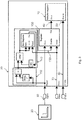
- An intermediate register 100 which can also be regarded as a second shadow register, is connected to the signal 30 and the shadow register 10. Current signal values can be stored in the intermediate register 100 while the shadow register is decoupled.
- a two-part logic circuit 110, 140 is connected to the signal 30 and the intermediate register 100. The first part of the logic circuit 110 detects at runtime that a change in the signal value has taken place. The second part of the logic circuit 140 generates a trigger signal 130, which serves as an enable signal for the second register, when a signal value change is detected by the first part of the logic circuit 110.
- the logic circuit 110, 140 is constructed in such a way that the trigger signal 130 is generated for only one cycle when the signal value changes. As a result, only the first changed signal value is stored in the intermediate register 100.
- the enable signal 60 enables the signal value stored in the intermediate register 100 to be transferred to the shadow register 10. The value can then be read from the shadow register 100, for example via a readback interface.
- the enable signal 60 also serves as a reset signal for the logic circuit 110, 140 and the intermediate register 100.
- the logic circuit 110 140 is designed such that it generates a new trigger signal 130 only after the reset signal has been received. The reset of the intermediate register 100 makes it possible to clearly distinguish in the data read out whether a current value has been read out or only the initialization value of the register after a reset.
- trigger signal 130 can also be forwarded to other inserted circuits.
- a trigger signal can trigger the storage of a large number of signal values. This is beneficial when a consistent set of signal values that are simultaneously present in the FPGA is to be acquired.
- the part 70 inserted during the method in this example comprises the shadow register 10, the intermediate register 100 and the two-part logic circuit 110, 140.
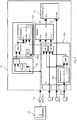
- the enable signal 60 is not used here as a reset signal for the second register 100 and the two-part logic circuit 110, 140.
- the enable signal 60 is only used to transfer the signal value to the shadow register 10.
- the reset signal 70 for the Logic circuit 110, 140 and the intermediate register 100 are separate from the enable signal 60 and can be controlled from outside or inside the FPGA, depending on the implementation.
- a fourth embodiment is shown. Only the differences to the illustration of the Figure 3 explained.
- a mode switching logic 200 is inserted.
- the mode switching logic 200 receives the reset signal 70, the enable signal 60 and a mode signal 210 as inputs.
- the two-part logic circuit 110, 140 can be overridden, so that the circuit of the fourth embodiment is like the circuit of the first embodiment Figure 1 behaves.
- the enable signal 60 is used as a reset signal for the intermediate register 100 and the two-part logic circuit 110, 140, so that the circuit is like the circuit of the second embodiment Figure 2 behaves. If no mode signal 210 is present, the circuit behaves like the circuit of the third embodiment Figure 3 .
- the fourth embodiment thus represents a combination of the first three embodiments, the behavior can be selected by the mode signal 210 at runtime. This is advantageous if it is not yet clear which behavior is required when the netlist is created.
- FIG. 5 shows a schematic representation of the behavior of the first, second and third embodiment.
- the top line 500 shows an exemplary signal profile of the signal 30. Over time, the signal value changes several times between 0 and 1.
- the second line 510 shows the value of the shadow register 10 using the example of the first exemplary embodiment Figure 1 .
- the enable signal 60 is briefly activated at four different times 550, 560, 570, 580. Since the value of the shadow register is only updated when the enable signal 60 is active, the value of the shadow register 10 remains 0 until the signal value 30 is 1 and the enable signal is active at the same time. The value can then be read from the shadow register.
- the third line 520 shows the value of the intermediate register 100 using the example of the third exemplary embodiment Figure 3 .
- the two-part logic circuit 110, 140 triggers the trigger signal 130 and the current value is transferred to the intermediate register 100.
- the reset signal 70 becomes active at a fifth point in time 590.
- the reset signal 70 sets the value of the intermediate register 100 to 0 and resets the two-part logic circuit 110, 140, so that the next time the signal value of the signal 30 changes, a trigger signal 130 is generated again. Every time the enable signal 60 is active at one of the four indicated times 550, 560, 570, 580, the current value of the intermediate register 100 at these times is transferred to the shadow register 10 and can be read from there.
- the fourth line 530 shows the value of the intermediate register 100 using the example of the second exemplary embodiment Figure 2 .
- the two-part logic circuit 110, 140 triggers the trigger signal 130 and the current value is transferred to the intermediate register 100. Every time the enable signal 60 is active at one of the four indicated times 550, 560, 570, 580, the current value of the intermediate register 100 at these times is transferred to the shadow register 10 and can be read from there.
- the enable signal 60 sets the value of the intermediate register 100 to 0 and resets the two-part logic circuit 110, 140, so that the next time the signal value of the signal 30 changes, a trigger signal 130 is generated again.
- Figure 6 shows a schematic representation of a network list, with preparation for reading out the registers via a readback interface.
- the network list consists of three logic blocks MUX, ADD, MULT and several lines. Two inputs 610, 620 of the network list are fed into two inputs of the first logic block MUX. The output of the first logic block MUX is connected to a first input of the second logic block ADD. A third input 630 of the network list is connected to a second input of the second logic block ADD. The output of the second logic block ADD is connected to a first input of the third logic block MULT.
- a fourth input 640 of the network list is connected to a second input of the third logic block MULT. The output of the third logic block forms the output of the network list.
- Each shadow register REG is assigned to an output signal of a logic block.
- the shadow registers REG are intended and set up for reading out via a readback interface, so no readout logic is added to the network list.
- the shadow registers can be functionally separated from the logic blocks via a decoupling circuit in the same clock step. This means that a consistent data record can be recorded in the shadow registers.
- Figure 7 shows a schematic decoupling circuit with interruption of the clock signal.
- the clock signal 700 of the shadow register is connected to the clock network CLK of the signal assigned to the shadow register via an inserted decoupling mechanism 710.
- the decoupling mechanism can be addressed from inside and / or outside the FPGA at runtime and interrupt the clock signal.
- the signal 30 assigned to the shadow register 10 from the FPGA source code 20 is permanently connected to the signal input 40 of the shadow register 10.
- the shadow register 10 only then takes a current one Signal value when the decoupling mechanism 700 connects the clock signal of the shadow register 10 to the clock network CLK.
- Figure 8 shows a schematic decoupling circuit with interruption of the enable signal.
- the clock signal 700 of the shadow register 10 is connected directly to the clock network CLK in this embodiment.
- a decoupling mechanism is inserted and connected to the enable input 50 of the shadow register 10.
- the decoupling mechanism can be addressed from inside and / or outside the FPGA at runtime and interrupt the enable signal.
- FPGA programs with multiple clock domains can also be operated safely in the ways described above, i.e. without metastable states.
- the shadow register when decoupling with interruption of the clock signal, the shadow register is connected to the clock network with which the assigned signal is also operated.
- the clock lines of the shadow registers are connected to the respective clock network of the assigned signals.
- a separate enable signal with correct clock domain transition is inserted for each clock domain in the FPGA network list and connected to the enable ports of the shadow register of the respective clock domains.
- a clock domain transition can, for example, be correctly exceeded by double registers.
- Figure 9 shows the steps of a method according to the invention. Some steps are mandatory, other steps are optional.
- a copy of the source code is created.
- the minimum required bit widths of the constants in the source code or the copy of the source code are determined.
- the minimum required bit widths determined in the second step S120 are propagated by the source code.
- a signal 30 is determined to which a shadow register 10 is to be assigned. This step can done automatically by an algorithm or by user input.
- a fifth optional step S150 it is checked whether the value of the signal determined in the fourth step S140 can be determined from values of already inserted shadow registers.
- a shadow register 10 is inserted for the signal 30 determined in the fourth step S140.
- a decoupling mechanism is inserted and set up for the shadow register 10, or the shadow register 10 is connected to an already inserted decoupling mechanism. If it was found in the fifth step S150 that the value of the signal 30 determined in the fourth step S140 can be determined from already inserted shadow registers, then in the sixth step S160 no shadow register is inserted, but referenced to the already inserted shadow registers from which the value is derived of the signal can be determined.
- a read-out mechanism is inserted and set up for the shadow register 10 inserted in the sixth step S160.
- Inserting and setting up the read-out mechanism can, for example, consist in inserting an instruction to the implementation tools in the source code, stating that reading via a readback interface should be enabled on the FPGA onto which the netlist is to be loaded.
- the fourth through seventh steps can be repeated several times in order to assign shadow registers to a large number of signals.
- the fourth to seventh steps are preferably processed repeatedly in an automated manner by an algorithm, the algorithm systematically processing all signals defined in the source code.
- a network list is synthesized from the source code. It should be noted that the eighth step S180 can also be carried out before the fourth step S140. In any case, the netlist contains both the information of the original source code and the inserted shadow registers with the set up decoupling mechanism and the set up readout mechanism.
- the network list generated in the eighth step S180 is converted into a bit stream, which is then converted into a optional tenth step S200 can be loaded onto an FPGA and executed there.
- the shadow register 10 inserted in the sixth step S160 can be decoupled from the function of the original source code via the decoupling mechanism and read out via the readout mechanism set up in the seventh step S170.
- the oligatory steps of the method enable the value of the signal 30 determined in the fourth step S140 to be reliably read out during the runtime of the FPGA.
Landscapes
- Engineering & Computer Science (AREA)
- Computer Hardware Design (AREA)
- Physics & Mathematics (AREA)
- Theoretical Computer Science (AREA)
- Evolutionary Computation (AREA)
- Geometry (AREA)
- General Engineering & Computer Science (AREA)
- General Physics & Mathematics (AREA)
- Logic Circuits (AREA)
- Stored Programmes (AREA)
Description
Die vorliegende Erfindung betrifft ein Verfahren zur Erstellung einer Netzliste für ein FPGA.The present invention relates to a method for creating a network list for an FPGA.
Die Echtzeitsimulation von komplexen, dynamischen Modellen stellt aufgrund der engen zeitlichen Randbedingungen selbst an moderne Rechenknoten hohe Anforderungen. In automotiven Hardware-in-the-Loop-Simulationen (HiL) werden solche Modelle vor allem dort eingesetzt, wo schnelle Regelkreise geschlossen werden müssen. Dies ist etwa bei der Simulation von Zylinderinnendrucksensoren der Fall, die bei der Verbrauchs- oder Abgasreduktion eine zunehmend größere Rolle spielen. Aber auch bei Regelstrecken die eine hohe Dynamik aufweisen, wie zum Beispiel bei Elektromotoren, sind kurze Zykluszeiten und geringe Latenzen unabdingbar. Diese können mit CPU-basierten Simulationen praktisch kaum mehr umgesetzt werden.The real-time simulation of complex, dynamic models places high demands on even modern computing nodes due to the tight time constraints. In automotive hardware-in-the-loop simulations (HiL), such models are mainly used where fast control loops have to be closed. This is the case, for example, with the simulation of internal cylinder pressure sensors, which play an increasingly important role in reducing consumption or exhaust gas. Short cycle times and low latencies are also essential for controlled systems that have a high level of dynamics, such as electric motors. In practice, these can hardly be implemented with CPU-based simulations.
Field Programmable Gate Arrays (FPGAs) können Rechenknoten bei der Echtzeitsimulation unterstützen, indem sie die Berechnung von dynamischen Teilen eines Modells übernehmen. Durch die hohe Flexibilität und Möglichkeit der Parallelverarbeitung von Signalen lassen sich durch den Einsatz von FPGAs auch harte Echtzeitanforderungen leicht erfüllen. Die FPGAs können als Hardwarebeschleuniger für CPUs von Rechenknoten dienen. Entsprechend werden z.B. sehr dynamische Teile des Umgebungsmodells in das FPGA ausgelagert, so dass ausreichend präzise und schnelle Reaktionszeiten für das Steuergerät gewährleistet bleiben. Eine FPGA-Netzliste wird üblicherweise basierend auf einem FPGA Modell in einer Hardwarebeschreibungssprache in einem Build-Prozess erzeugt.Field Programmable Gate Arrays (FPGAs) can support computing nodes in real-time simulation by taking over the calculation of dynamic parts of a model. Due to the high flexibility and the possibility of parallel processing of signals, even hard real-time requirements can easily be met through the use of FPGAs. The FPGAs can serve as hardware accelerators for CPUs of computing nodes. Accordingly, very dynamic parts of the environment model, for example, are outsourced to the FPGA, so that sufficiently precise and fast response times for the control unit are guaranteed. An FPGA network list is usually generated in a build process based on an FPGA model in a hardware description language.
Die Modelle einer Regelstrecke werden durch steigende Anforderungen an die Genauigkeit zunehmend komplexer und somit auch schwer handhabbar. Im automotiven Hil-Umfeld werden solche Modelle in der Regel mit dem Toolset Matlab/Simulink von The MathWorks Inc. erstellt. Simulink bietet eine blockbasierte Sicht in der Form eines Blockschaltbilds auf solche Modelle. Modellteile können in einem Blockschaltbild zu Subsystemen zusammengefasst und untereinander mit Signalen verknüpft werden. Der Datenfluss zwischen diesen Blöcken wird dabei über Signalleitungen dargestellt.The models of a controlled system are becoming more and more complex and therefore difficult to handle due to increasing demands on accuracy. In the automotive Hil environment, such models are usually created with the Matlab / Simulink toolset from The MathWorks Inc. Simulink offers a block-based view of such models in the form of a block diagram. Model parts can become subsystems in a block diagram summarized and linked with each other with signals. The data flow between these blocks is displayed via signal lines.
Eine FPGA-basierte Simulation kann unter Zuhilfenahme des Xilinx System Generator (XSG) und des FPGA-Programming Blocksets von dSPACE, analog zur CPU-basierten Simulation, in einem Blockschaltbild mit Simulink modelliert werden.An FPGA-based simulation can be modeled in a block diagram with Simulink using the Xilinx System Generator (XSG) and the FPGA programming block set from dSPACE, analogous to the CPU-based simulation.
Im Gegensatz zur CPU-Simulation wird dieses Modell allerdings nicht in eine iterative Programmiersprache übersetzt, sondern in eine FPGA-Netzliste, die eine kundenspezifische digitale Schaltung beschreibt. Die FPGA-Netzliste kann in einen FPGA-Konfigurationsdatenstrom übersetzt werden.In contrast to the CPU simulation, this model is not translated into an iterative programming language, but into an FPGA network list that describes a customer-specific digital circuit. The FPGA netlist can be translated into an FPGA configuration data stream.
Aus der
Aus der
Bei einigen Auslesetechniken werden die Daten direkt aus den Arbeitsregistern ausgelesen. Beim Auslesen zur Laufzeit des FPGAs ist dies nachteilig, da es häufig nicht möglich ist, ein Register zu einem speziellen Zeitpunkt auszulesen. Da die Arbeitsregister zur Laufzeit ständig mit aktuellen Werten überschrieben werden, kann ein zu einem speziellen Zeitpunkt vorliegender Wert häufig nicht erfasst werden.With some readout techniques, the data is read out directly from the working registers. When reading out during the runtime of the FPGA, this is disadvantageous because it is often not possible to read out a register at a specific point in time. Since the working registers are constantly overwritten with current values during runtime, a value that is available at a specific point in time often cannot be recorded.
Aufgabe der Erfindung ist es, den Stand der Technik weiterzubilden.The object of the invention is to develop the state of the art.
Die Erfindung betrifft ein Verfahren zum Erstellen einer FPGA-Netzliste, wobei die Netzliste aus einem FPGA-Quellcode und zumindest einem Schattenregister erzeugt wird,
wobei der FPGA-Quellcode zumindest eine Funktion und zumindest ein Signal definiert,
wobei das Schattenregister dem zumindest einen Signal zugeordnet wird und dazu eingerichtet und vorgesehen wird den Wert des zugeordneten Signals zur Laufzeit zu speichern,
wobei eine Möglichkeit zum Auslesen des gespeicherten Signalwertes zur Laufzeit vorgesehen und eingerichtet wird,
wobei die im FPGA-Quellcode definierte Funktion durch das Schattenregister nicht verändert wird,
wobei die Netzliste dazu vorgesehen wird auf einen FPGA geladen und von dem FPGA ausgeführt zu werden,
wobei die vom FPGA-Quellcode beschriebene Funktion vom FPGA ausgeführt wird,
wobei eine funktionale Abkopplung des Schattenregisters von der im FPGA-Quellcode beschriebenen Funktion vorgesehen und eingerichtet wird,
wobei das Schattenregister durch die Abkopplung den zum Zeitpunkt der Abkopplung gespeicherten Signalwert beibehält, während die im FPGA-Quellcode beschriebene Funktion ausgeführt wird.The invention relates to a method for creating an FPGA network list, the network list being generated from an FPGA source code and at least one shadow register,
wherein the FPGA source code defines at least one function and at least one signal,
wherein the shadow register is assigned to the at least one signal and is set up and provided to store the value of the assigned signal at runtime,
a possibility for reading out the stored signal value at runtime is provided and set up,
where the function defined in the FPGA source code is through the shadow register is not changed,
The netlist is intended to be loaded onto an FPGA and executed by the FPGA,
where the function described by the FPGA source code is carried out by the FPGA,
a functional decoupling of the shadow register from the function described in the FPGA source code is provided and set up,
whereby the shadow register retains the signal value stored at the time of the uncoupling due to the decoupling, while the function described in the FPGA source code is carried out.
Erfindungsgemäß ist ferner eine Datenverarbeitungseinrichtung mit einer Prozessoreinheit angegeben, wobei die Datenverarbeitungseinrichtung zur Durchführung des obigen Verfahrens ausgeführt ist.According to the invention, a data processing device with a processor unit is also specified, the data processing device being designed to carry out the above method.
Erfindungsgemäß ist auch ein Computerprogrammprodukt mit Computerimplementierten Anweisungen, das nach dem Laden und Ausführen in einer geeigneten Datenverarbeitungseinrichtung die Schritte des obigen Verfahrens ausführt, angegeben.According to the invention, a computer program product with computer-implemented instructions is also specified which, after loading and execution in a suitable data processing device, executes the steps of the above method.
Weiterhin ist erfindungsgemäß ein digitales Speichermedium mit elektronisch auslesbaren Steuersignalen angegeben, die so mit einer programmierbaren Datenverarbeitungseinrichtung zusammenwirken können, dass das obige Verfahren auf der Datenverarbeitungseinrichtung ausgeführt wird.Furthermore, according to the invention, a digital storage medium with electronically readable control signals is specified which can interact with a programmable data processing device in such a way that the above method is carried out on the data processing device.
Die Netzliste kann in einen Bitstrom umgewandelt und auf einen FPGA geladen werden. Der FPGA kann dann die im FPGA-Quellcode definierte Funktion ausführen. Durch die Abkopplung wird es möglich genau den Wert auszulesen, der zum Zeitpunkt der Abkopplung aktuell war, auch dann, wenn ein Auslesen der Signalwerte verzögert erfolgt. Zur Laufzeit ist hier so zu verstehen, dass die im FPGA-Quellcode definierte Funktion weiterhin ausgeführt wird und der Signalwert weiterhin aktualisiert wird, während der das Schattenregister abgekoppelt wird und den zum Zeitpunkt der Abkopplung aktuellen Wert beibehält. Die Abkopplung wird vorzugsweise durch ein Triggersignal ausgelöst. In der FPGA-Netzliste wird dazu der Abkopplungsmechanismus mit dem Triggersignal verbunden. Alternativ kann das Schattenregister standardmäßig abgekoppelt sein und auf ein Triggersignal hin kurzzeitig mit der Funktion verbunden werden. Dann wird im Schattenregister der zum Zeitpunkt des Triggersignals aktuelle Signalwert gespeichert und das Schattenregister wieder von der Funktion abgekoppelt.The netlist can be converted into a bit stream and loaded onto an FPGA. The FPGA can then perform the function defined in the FPGA source code. The decoupling makes it possible to read out exactly the value that was current at the time of the decoupling, even if the signal values are read out with a delay. At runtime it should be understood that the function defined in the FPGA source code continues to be executed and the signal value continues to be updated during which the shadow register is decoupled and that at the time of Uncoupling maintains current value. The decoupling is preferably triggered by a trigger signal. For this purpose, the decoupling mechanism is linked to the trigger signal in the FPGA network list. Alternatively, the shadow register can be decoupled by default and briefly connected to the function in response to a trigger signal. The current signal value at the time of the trigger signal is then stored in the shadow register and the shadow register is decoupled from the function again.
Das Ergebnis des erfindungsgemäßen Verfahrens ist folglich eine FPGA-Netzliste, wobei in der Netzliste zumindest ein Schattenregister definiert ist, wobei in der FPGA-Netzliste zumindest eine Funktion und zumindest ein Signal definiert ist, wobei das Schattenregister mit dem zumindest einen Signal verbunden ist und dazu eingerichtet und vorgesehen ist den Wert des Signals zur Laufzeit zu speichern, wobei die Netzliste dazu vorgesehen ist auf einen FPGA geladen und von dem FPGA ausgeführt zu werden, wobei eine Möglichkeit zum Auslesen des in dem Schattenregister gespeicherten Signalwerts zur Laufzeit des FPGA in der Netzliste vorgesehen und eingerichtet ist, wobei eine funktionale Abkopplung des Schattenregisters von dem Signal vorgesehen und eingerichtet ist, wobei das Schattenregister durch die Abkopplung den zum Zeitpunkt der Abkopplung gespeicherten Signalwert beibehält, während das FPGA die Funktion ausführt.The result of the method according to the invention is consequently an FPGA network list, with at least one shadow register being defined in the network list, with at least one function and at least one signal being defined in the FPGA network list, with the shadow register being connected to the at least one signal and in addition The value of the signal is set up and intended to be stored at runtime, the netlist being loaded onto an FPGA and executed by the FPGA, with the possibility of reading out the signal value stored in the shadow register at runtime of the FPGA in the netlist and is set up, wherein a functional decoupling of the shadow register from the signal is provided and set up, the shadow register retaining the signal value stored at the time of the decoupling as a result of the decoupling while the FPGA is executing the function.
In einer bevorzugten Ausgestaltung definiert der FPGA-Quellcode ein Vielzahl von Signalen, wobei eine Vielzahl von Schattenregistern jeweils einem Signal zugeordnet wird, wobei die funktionale Abkopplung dazu vorgesehen ist die Vielzahl an Schattenregistern synchron abzukoppeln.In a preferred embodiment, the FPGA source code defines a multiplicity of signals, a multiplicity of shadow registers being assigned to one signal in each case, the functional decoupling being provided for synchronously decoupling the multiplicity of shadow registers.
Durch die synchrone Abkopplung wird es möglich eine Vielzahl von zeitgleich vorliegenden Signalwerten zur Laufzeit aus dem FPGA auszulesen. Das synchrone Auslesen mehrere Signalwerte aus einem FPGA ist häufig nicht möglich. Durch die synchron abkoppelbaren Schattenregister können zeitgleich vorliegende Signalwerte gespeichert und nacheinander ausgelesen werden. So kann ein konsistenter Datensatz von gleichzeitig vorliegenden Variablen festgehalten werden.The synchronous decoupling makes it possible to read out a large number of signal values present at the same time from the FPGA during runtime. The synchronous reading of several signal values from an FPGA is often not possible. The synchronously decoupled shadow register allows signal values present at the same time to be saved and read out one after the other. In this way, a consistent data set of simultaneously available variables can be retained.
Das Ergebnis der bevorzugten Ausgestaltung ist eine FPGA-Netzliste, wobei in der FPGA-Netzliste eine Vielzahl von Signalen definiert ist, wobei eine Vielzahl von Schattenregistern jeweils einem Signal zugeordnet ist, wobei die funktionale Abkopplung dazu vorgesehen ist die Vielzahl von Schattenregistern synchron abzukoppeln.The result of the preferred embodiment is an FPGA network list, a plurality of signals being defined in the FPGA network list, a plurality of shadow registers being assigned to one signal, the functional decoupling being provided to decouple the plurality of shadow registers synchronously.
In einer Ausgestaltung wird zur Abkopplung das enable-Signal des Schattenregisters oder das Taktsignal des Schattenregisters unterbrochen.In one embodiment, the enable signal of the shadow register or the clock signal of the shadow register is interrupted for decoupling.
Durch die Unterbrechung des enable-Signals des Schattenregisters wird das Schattenregister zur Laufzeit nicht mehr aktualisiert. Dies stellt eine sehr einfache Möglichkeit der Abkopplung für ein oder mehrere Schattenregister dar.Due to the interruption of the enable signal of the shadow register, the shadow register is no longer updated during runtime. This is a very simple way of decoupling one or more shadow registers.
Durch die Unterbrechung des Clock-Signals des Schattenregisters, nimmt das Schattenregister keine Änderungen mehr an, sodass der Zustand des Registers quasi eingefroren wird. Der im Schattenregister gespeicherte Wert kann dennoch auf verschiedene Arten ausgelesen werden.By interrupting the clock signal of the shadow register, the shadow register no longer accepts any changes, so that the state of the register is more or less frozen. The value stored in the shadow register can still be read out in various ways.
Das Ergebnis der bevorzugten Ausgestaltung ist eine FPGA-Netzliste, wobei in der Netzliste vorgesehen ist zur Abkopplung das enable-Signal des Schattenregisters oder das Clock-Signal des Schattenregisters zu unterbrechen.The result of the preferred refinement is an FPGA network list, the network list providing to interrupt the enable signal of the shadow register or the clock signal of the shadow register for decoupling.
In einer Ausgestaltung liegt der FPGA-Quellcode als grafisches Modell oder als textueller Code vor.In one embodiment, the FPGA source code is available as a graphic model or as textual code.
FPGA-Quellcode liegt häufig in Form eines grafischen Modells vor, beispielsweise als Blockdiagramm in einer Entwicklungsumgebung. Beispiele für solche Blockdiagramme ist Simulink von The MathWorks. In grafischen Quellcode lassen sich Schattenregister leicht als zusätzliche Register einfügen, wobei die zusätzlichen Register mit dem zugeordneten Signal verbunden werden und über einen ebenfalls eingefügten Abkoppelmechanismus zur Laufzeit funktional vom Signal abgekoppelt werden können.FPGA source code is often in the form of a graphical model, such as a block diagram in a development environment. Examples of such block diagrams is Simulink from The MathWorks. In graphical source code, shadow registers can easily be inserted as additional registers, whereby the additional registers are connected to the assigned signal and can be functionally decoupled from the signal during runtime using a decoupling mechanism that has also been inserted.
Eine alternative Form von FPGA-Quellcode ist textueller Code, beispielsweise VHDL oder Verilog. Auch in textuellen Quellcode lassen sich Schattenregister leicht als zusätzliche Register einfügen, wobei die zusätzlichen Register mit dem zugeordneten Signal verbunden werden und über einen ebenfalls eingefügten Abkoppelmechanismus zur Laufzeit funktional vom Signal abgekoppelt werden können.An alternative form of FPGA source code is textual code, for example VHDL or Verilog. Shadow registers can also be easily inserted as additional registers in textual source code, whereby the additional registers are connected to the assigned signal and can be functionally decoupled from the signal at runtime using a decoupling mechanism that has also been inserted.
In einer bevorzugten Ausgestaltung wird das Schattenregister in den FPGA-Quellcode oder eine Kopie des FPGA-Quellcodes eingefügt wird.In a preferred embodiment, the shadow register is inserted into the FPGA source code or a copy of the FPGA source code is inserted.
Durch das Einfügen des Schattenregisters direkt in den FPGA-Quellcode ist die Erstellung einer Netzliste besonders einfach, da nur der FPGA-Quellcode in eine Netzliste übersetzt werden muss. Durch das Einfügen des Schattenregisters in eine Kopie des FPGA-Quellcodes bleibt der ursprüngliche FPGA-Quellcode unangetastet. Dies ist vorteilhaft, wenn das Verfahren für den Nutzer transparent sein soll. Der Nutzer bekommt also nicht mit, dass ein Schattenregister eingefügt wurde, die Vorteile beim Auslesen des Signalwertes zur Laufzeit können trotzdem genutzt werden.By inserting the shadow register directly into the FPGA source code, creating a network list is particularly easy, since only the FPGA source code has to be translated into a network list. By inserting the shadow register into a copy of the FPGA source code, the original FPGA source code remains untouched. This is advantageous if the method is to be transparent to the user. The user does not notice that a shadow register has been inserted, the advantages of reading out the signal value during runtime can still be used.
In einer alternativen Ausgestaltung wir aus dem Quellcode eine Netzliste generiert und das Schattenregister in die Netzliste eingefügt.In an alternative embodiment, a network list is generated from the source code and the shadow register is inserted into the network list.
Durch das Einfügen der Schattenregister in die Netzliste bleibt der FPGA-Quellcode unverändert ohne dass eine Kopie angelegt werden muss. Die Netzliste mit den Schattenregistern kann danach wie jede andere Netzliste weiterverwendet werden. Beispielsweise kann sie in einen Bitstrom umgewandelt werden und auf anschließend auf einen FPGA geladen werden. Die Netzliste in die das Schattenregister eingefügt wird kann hierbei als einfache Netzliste oder mit Zusatzinformationen über Mapping, Placing und/oder Routing vorliegen.By inserting the shadow register in the network list, the FPGA source code remains unchanged without having to make a copy. The netlist with the shadow registers can then be used like any other netlist. For example, it can be converted into a bit stream and then loaded onto an FPGA. The network list into which the shadow register is inserted can be present as a simple network list or with additional information about mapping, placing and / or routing.
In einer bevorzugten Ausgestaltung wird das Schattenregister automatisiert eingefügt und dem Signal zugeordnet.In a preferred embodiment, the shadow register is automatically inserted and assigned to the signal.
Durch die Automatisierung wird der Nutzer von der Aufgabe entlastet das Schattenregister einzufügen und dem Signal zuzuordnen. Insbesondere bei einer Vielzahl von Signalen, denen jeweils ein Schattenregister zugeordnet werden soll ist die Automatisierung von großem Vorteil.The automation relieves the user of the task of inserting the shadow register and assigning it to the signal. Automation is of great advantage, especially when there are a large number of signals, each of which is to be assigned a shadow register.
In einer weiteren Ausgestaltung wird automatisiert geprüft, ob das Signal bereits an anderer Stelle einem Schattenregister zugeordnet ist und dann diesem Signal kein weiteres Schattenregister zugeordnet.In a further embodiment, an automated check is carried out to determine whether the signal is already assigned to a shadow register elsewhere and then no further shadow register is assigned to this signal.
Durch die automatisierte Prüfung wird verhindert, dass für ein Signal eine Vielzahl von Schattenregistern eingefügt und dem Signal zugeordnet werden. Insbesondere wenn der FPGA-Quellcode groß wird, also viele Zeilen Text umfasst oder als grafisches Modell eine Vielzahl von Hierarchieebenen umfasst ist eine manuelle Prüfung aufwendig und fehleranfällig und daher die automatisierte Prüfung vorteilhaft.The automated test prevents a large number of shadow registers from being inserted and assigned to the signal for a signal. In particular if the FPGA source code is large, that is to say comprises many lines of text or comprises a large number of hierarchical levels as a graphic model, manual testing is time-consuming and error-prone, and automated testing is therefore advantageous.
In einer weiteren Ausgestaltung werden mindestens zwei Schattenregister eingefügt und dem Signal zugeordnet, wobei das erste Schattenregister dazu vorgesehen und eingerichtet wird zur Laufzeit einen aktuellen Signalwert zu speichern, während das zweite Schattenregister abgekoppelt ist.In a further embodiment, at least two shadow registers are inserted and assigned to the signal, the first shadow register being provided and set up to store a current signal value at runtime, while the second shadow register is decoupled.
Mit zwei Schattenregistern ist es möglich einen alten Signalwert im ersten Schattenregister festzuhalten und gleichzeitig einen aktuellen Signalwert im zweiten Schattenregister aufzunehmen. Dies kann zum Beispiel eingesetzt werden, wenn der Auslesevorgang der Schattenregister mehrere FPGA-Takte dauert oder nicht sofort durchgeführt werden kann. Dann kann während des Auslesens des ersten Schattenregisters ein aktueller Wert im zweiten Schattenregister gespeichert werden.With two shadow registers it is possible to hold an old signal value in the first shadow register and at the same time record a current signal value in the second shadow register. This can be used, for example, if the readout process of the shadow register takes several FPGA cycles or cannot be carried out immediately. A current value can then be stored in the second shadow register while the first shadow register is being read out.
Mehrere Schattenregister können auch ein Speicherfenster darstellen. In dem Fall wird in einem Schattenregister ein aktueller Signalwert gespeichert und in dem anderen Schattenregister ein alter Signalwert. Auf ein Triggersignal hin können die Schattenregister gleichzeitig abgekoppelt werden. Dadurch wird es möglich den Signalwert vor dem Triggersignal auszulesen.Multiple shadow registers can also represent a memory window. In this case, a current signal value is stored in one shadow register and an old signal value is stored in the other shadow register. The shadow registers can be decoupled at the same time in response to a trigger signal. This makes it possible to read out the signal value before the trigger signal.
In einer alternativen Ausführungsform kann ein Speicherfenster genutzt werden, um einen auf ein Triggersignal folgenden Signalwert festzuhalten. In dem Fall werden die Schattenregister nacheinander nach einer vorbestimmten Zeitdauer abgekoppelt.
Durch drei oder mehr Schattenregister können beide Varianten gleichzeitig genutzt werden. So wird es möglich, den Signalwert vor und nach einem Triggersignal festzuhalten und auszulesen.In an alternative embodiment, a memory window can be used to hold a signal value following a trigger signal. In that case, the shadow registers are disconnected one after the other after a predetermined period of time.
With three or more shadow registers, both variants can be used at the same time. This makes it possible to record and read out the signal value before and after a trigger signal.
Das Ergebnis der bevorzugten Ausgestaltung ist eine FPGA-Netzliste, wobei in der FPGA-Netzliste mindestens zwei Schattenregister definiert sind und dem einen Signal zugeordnet sind, wobei das erste Schattenregister dazu vorgesehen und eingerichtet ist zur Laufzeit einen aktuellen Signalwert zu speichern, während das zweite Schattenregister abgekoppelt ist.The result of the preferred refinement is an FPGA network list, at least two shadow registers being defined in the FPGA network list and being assigned to one signal, the first shadow register being provided and set up to store a current signal value at runtime, while the second shadow register is disconnected.
In einer besonders bevorzugten Ausgestaltung wird beim Erstellen der Netzliste ein Auslesen des Schattenregisters über eine externe und/oder interne Readbackschnittstelle des FPGAs vorgesehen und eingerichtet.In a particularly preferred embodiment, when the network list is being created, reading out the shadow register via an external and / or internal readback interface of the FPGA is provided and set up.
Das Auslesen der Schattenregister über eine interne oder externe Readbackschnittstelle stellt eine komfortable Möglichkeit des Auslesens dar. Bei dieser Ausführungsform werden insbesondere sehr wenig Logik und Routingressourcen des FPGAs für das Auslesen benötigt. Das Schattenregister kann durch die Implemenierungswerkzeuge direkt neben das zugeordnete Signal platziert werden. Dadurch ist die Änderung gegenüber einer Netzliste ohne eingefügtes Schattenregister minimal.Reading out the shadow register via an internal or external readback interface is a convenient way of reading out. In this embodiment, in particular, very little logic and routing resources of the FPGA are required for reading out. The shadow register can be placed directly next to the assigned signal using the implementation tools. As a result, the change compared to a network list without an inserted shadow register is minimal.
In einer weiteren Ausgestaltung wird eine Vielzahl von Schattenregistern eingefügt, wobei die Vielzahl von Schattenregistern zu einer Schieberegisterkette verbunden werden und dazu vorgesehen und eingerichtet werden über eine externe Schnittstelle des FPGAs ausgelesen zu werden.In a further refinement, a plurality of shadow registers is inserted, the plurality of shadow registers becoming one Shift register chain are connected and provided and set up to be read out via an external interface of the FPGA.
In einer alternativen Ausgestaltung wird eine Vielzahl von Schattenregistern eingefügt, wobei ein Adressdecoder zum Auslesen der Vielzahl von Schattenregistern über eine externe Schnittstelle des FPGA vorgesehen und eingerichtet wird.In an alternative embodiment, a large number of shadow registers are inserted, an address decoder being provided and set up for reading out the large number of shadow registers via an external interface of the FPGA.
Das Auslesen über eine externe Schnittstelle ermöglicht typischerweise einen höheren Datendurchsatz als eine Readbackschnittstelle. Daher ist diese Form des Auslesens vorteilhaft, wenn zur Laufzeit häufig viele Signalwerte ausgelesen werden sollen.Reading out via an external interface typically enables a higher data throughput than a readback interface. This form of reading is therefore advantageous if a large number of signal values are often to be read out during runtime.
In einer weiteren Ausgestaltung wird zusätzlich zum Schattenregister eine Logik eingefügt, wobei die Logik dazu vorgesehen und eingerichtet wird zur Laufzeit bei einer Änderung des Signalwertes ein Triggersignal auszugeben, wobei das Triggersignal eine Abkopplung des Schattenregisters bewirkt.In a further embodiment, a logic is inserted in addition to the shadow register, the logic being provided and set up to output a trigger signal at runtime when the signal value changes, the trigger signal causing the shadow register to be decoupled.
Durch die eingebaute Logik kann die Abkopplung sehr schnell bei Auftreten vorbestimmter Ereignisse ausgelöst werden. Das Triggersignal kann dann die Abkopplung eines oder mehrerer Schattenregister sofort oder mit einer vorbestimmten Verzögerung auslösen. Eine solche Logik kann auf verschiedene Arten implementiert werden. Beispiele dazu finden sich in den Ausführungsbeispielen.Due to the built-in logic, the decoupling can be triggered very quickly when predetermined events occur. The trigger signal can then trigger the uncoupling of one or more shadow registers immediately or with a predetermined delay. Such logic can be implemented in a number of ways. Examples of this can be found in the exemplary embodiments.
In einer bevorzugten Ausgestaltung werden vor dem Einfügen des Schattenregisters folgende Schritte durchgeführt werden:
- Ermitteln aller Konstanten im FPGA-Quellcode von denen der erste Signalwert abhängt,
- Ermitteln der minimal erforderlichen Bitbreiten für die gefundenen Werte der Konstanten
- Umkonfiguration der Konstanten auf die jeweils ermittelte minimal erforderliche Bitbreite oder nachträgliches Casting der Konstanten auf die jeweils ermittelte minimale erforderliche Bitbreite
- Durchpropagierung der Bitbreiten durch das gesamte FPGA Modell.
- Determination of all constants in the FPGA source code on which the first signal value depends,
- Determination of the minimum required bit widths for the found values of the constants
- Reconfiguration of the constants to the minimum determined in each case required bit width or subsequent casting of the constants to the minimum required bit width determined in each case
- Propagation of the bit widths through the entire FPGA model.
Konstantenblöcke in graphischen FPGA Modellen, bzw. VHDL Signale in VHDL Modellen werden häufig mit fester Bitbreite (z.B. 32 Bit) instanziiert. Bei der anschließenden Festlegung der Werte kommen jedoch meistens Werte zum Einsatz, die den Wertebereich der angegebenen Bitbreite nicht ausreizen. Der aus dem graphischen Modell generierte VHDL Code enthält ebenfalls die vollen Bitbreiten, unabhängig von den tatsächlich benötigten Bitbreiten. Bei der Handprogrammierung von VHDL Code geht man in der Regel ebenso vor.Constant blocks in graphic FPGA models or VHDL signals in VHDL models are often instantiated with a fixed bit width (e.g. 32 bits). When subsequently specifying the values, however, values are usually used that do not exhaust the value range of the specified bit width. The VHDL code generated from the graphic model also contains the full bit widths, regardless of the bit widths actually required. The manual programming of VHDL code is usually done in the same way.
Das ist normalerweise kein Problem, da die nicht benötigten Bits durch Synthese- und Implementierungswerkzeuge wegoptimiert werden, um Logik- und Routingressourcen einzusparen.This is usually not a problem, since the bits that are not required are optimized away by synthesis and implementation tools in order to save logic and routing resources.
Die eingefügten Schattenregister, die zum Auslesen über eine externe Schnittstelle eingerichtet sind, werden jedoch von den Synthese- und Implementierungswerkzeugen nicht optimiert, da diese Werkzeuge externe Zugänge nicht optimieren. Um den Ressourcenverbrauch durch die eingefügten Schattenregister und die Ausleselogik gering zu halten, ist es daher vorteilhaft die minimalerforderliche Bitbreite der Konstanten und aller von den Konstanten abhängigen Signale zu ermitteln. Dann kann das Schattenregister in der minimal benötigten Bitbreite des zugeordneten Signals implementiert werden.The inserted shadow registers, which are set up for reading out via an external interface, are not optimized by the synthesis and implementation tools, since these tools do not optimize external access. In order to keep the resource consumption by the inserted shadow registers and the readout logic low, it is therefore advantageous to determine the minimum required bit width of the constants and of all signals dependent on the constants. The shadow register can then be implemented in the minimum required bit width of the assigned signal.
In einer weiteren Ausgestaltung wird das Schattenregister vor einer Wegoptimierung bei der Erstellung und/oder Weiterverarbeitung der Netzliste geschützt.In a further refinement, the shadow register is protected from route optimization during the creation and / or further processing of the network list.
Register, die keine Ausgänge haben werden im Allgemeinen von den automatisierten Werkzeugen, die für die Erstellung und Weiterverarbeitung der Netzliste genutzt werden, wegoptimiert, d.h. gelöscht. Dies ist im Allgemeinen sinnvoll, da diese Register ansonsten Ressourcen im FPGA belegen ohne zu seiner Funktion beizutragen. Die im erfindungsgemäßen Verfahren eingefügten Schattenregister, die über eine Readbackschnittstelle ausgelesen werden sollen, haben keine Ausgänge und würden daher von den Werkzeugen gelöscht werden. Die Schattenregister werden allerdings benötigt, um die Signalwerte zur Laufzeit aus dem FPGA auslesen zu können. Daher ist es vorteilhaft die Schattenregister vor der Wegoptimierung zu schützen. Eine Möglichkeit dies zu erreichen ist es den Schattenregistern und den darin enthaltenen Signalen Attribute mitzugeben, wobei die Attribute von den Werkzeugen erkannt werden und die Werkzeuge dazu veranlasst keine Optimierungsmaßnahmen an den Registern vornehmen.Registers that have no outputs are generally optimized away, ie deleted, by the automated tools that are used for creating and further processing the network list. This is generally useful, as these registers would otherwise be resources in the FPGA prove without contributing to its function. The shadow registers inserted in the method according to the invention, which are to be read out via a readback interface, have no outputs and would therefore be deleted by the tools. However, the shadow registers are required in order to be able to read the signal values from the FPGA during runtime. It is therefore advantageous to protect the shadow registers from route optimization. One possibility to achieve this is to add attributes to the shadow registers and the signals contained therein, the attributes being recognized by the tools and the tools not causing any optimization measures to be carried out on the registers.
Eine Kombination der vor einer Wegoptimierung geschützten Schattenregister mit den oben genannten Schritten zur Ermittlung der minimal benötigten Bitbreite ist besonders vorteilhaft.A combination of the shadow registers protected from route optimization with the above-mentioned steps for determining the minimum required bit width is particularly advantageous.
Die Erfindung wird nachfolgend unter Bezugnahme auf die Zeichnungen näher erläutert. Hierbei werden gleichartige Teile mit identischen Bezeichnungen beschriftet. Die dargestellten Ausführungsformen sind stark schematisiert, d.h. die Abstände und die laterale und die vertikale Erstreckung sind nicht maßstäblich und weisen, sofern nicht anders angegeben auch keine ableitbare geometrische Relationen zueinander auf. Darin zeigt:
Figur 1- eine schematische Ansicht einer ersten erfindungsgemäßen Ausführungsform,
- Figur 2
- eine schematische Ansicht einer zweiten erfindungsgemäßen Ausführungsform,
- Figur 3
- eine schematische Ansicht einer dritten erfindungsgemäßen Ausführungsform,
- Figur 4
- eine schematische Ansicht einer vierten erfindungsgemäßen Ausführungsform
- Figur 5
- eine schematische Darstellung des Verhaltens der ersten, zweiten und dritten Ausführungsform
- Figur 6
- eine schematische Darstellung einer Netzliste, mit Vorbereitung für ein Auslesen der Register über eine Readbackschnittstelle
- Figur 7
- eine schematische Abkopplungsschaltung mit Unterbrechung der Clock-Leitung
- Figur 8
- eine schematische Abkopplungsschaltung mit Unterbrechung der enable-Leitung
- Figur 9
- die Schritte eines erfindungsgemäßen Verfahrens
- Figure 1
- a schematic view of a first embodiment of the invention,
- Figure 2
- a schematic view of a second embodiment of the invention,
- Figure 3
- a schematic view of a third embodiment of the invention,
- Figure 4
- a schematic view of a fourth embodiment of the invention
- Figure 5
- a schematic representation of the behavior of the first, second and third embodiment
- Figure 6
- a schematic representation of a network list, with preparation for reading out the registers via a readback interface
- Figure 7
- a schematic decoupling circuit with interruption of the clock line
- Figure 8
- a schematic decoupling circuit with interruption of the enable line
- Figure 9
- the steps of a method according to the invention
Das Verfahren wird in den
Die Abbildung der
In der Abbildung der
Es versteht sich, dass das Triggersignal 130 auch an andere eingefügte Schaltungen weitergeleitet werden kann. So kann ein Triggersignal die Speicherung einer Vielzahl von Signalwerten auslösen. Dies ist vorteilhaft, wenn ein konsistenter Satz von Signalwerten, die gleichzeitig im FPGA vorliegen, erfasst werden soll.It goes without saying that the
Der während des Verfahrens eingefügte Teil 70 umfasst in diesem Beispiel das Schattenregister 10, das Zwischenregister 100 und die zweiteilige Logikschaltung 110, 140.The
In der Abbildung der
In der Abbildung der
Die Abbildung in
Die oberste Zeile 500 zeigt einen beispielhaften Signalverlauf des Signal 30. Über die Zeit wechselt der Signalwert mehrfach zwischen 0 und 1.The
Die zweite Zeile 510 zeigt den Wert des Schattenregisters 10 am Beispiel des ersten Ausführungsbeispiels aus
Die dritte Zeile 520 zeigt den Wert des Zwischenregisters 100 am Beispiel des dritten Ausführungsbeispiels aus
Die vierte Zeile 530 zeigt den Wert des Zwischenregisters 100 am Beispiel des zweiten Ausführungsbeispiels aus
Zugleich setzt das enable-Signal 60 den Wert des Zwischenregisters 100 auf 0 und setzt die zweiteilige Logikschaltung 110, 140 zurück, sodass bei der nächsten Änderung des Signalwertes des Signals 30 wieder ein Triggersignal 130 erzeugt wird.At the same time, the enable
Auch FPGA-Programme mit mehreren Taktdomänen können auf die oben beschriebenen Arten sicher, d.h. ohne metastabile Zustände, betrieben werden. Dazu wird bei der Abkopplung mit Unterbrechung des Taktsignals das Schattenregister an das Taktnetz angeschlossen mit dem auch das zugeordnete Signal betrieben wird. Bei einer Vielzahl von Schattenregistern, die unterschiedlichen Signalen zugeordnet sind, werden die Taktleitungen der Schattenregister an das jeweilige Taktnetz der zugeordneten Signale angeschlossen. Bei der Abkopplung mit Unterbrechung der enable-Leitung wird für jede Taktdomäne in der FPGA-Netzliste ein eigenes Enable Signal mit korrektem Taktdomänenübergang eingefügt und an die Enable Ports der Schattenregister der jeweiligen Taktdomänen angeschlossen. Ein Taktdomänenübergang kann z.B. durch doppelte Register korrekt überschritten werden.FPGA programs with multiple clock domains can also be operated safely in the ways described above, i.e. without metastable states. For this purpose, when decoupling with interruption of the clock signal, the shadow register is connected to the clock network with which the assigned signal is also operated. In the case of a large number of shadow registers that are assigned to different signals, the clock lines of the shadow registers are connected to the respective clock network of the assigned signals. When decoupling with interruption of the enable line, a separate enable signal with correct clock domain transition is inserted for each clock domain in the FPGA network list and connected to the enable ports of the shadow register of the respective clock domains. A clock domain transition can, for example, be correctly exceeded by double registers.
In einem obligatorischen achten Schritt S180 wird aus dem Quellcode eine Netzliste synthetisiert. Es sei angemerkt, dass der achte Schritt S180 auch vor dem vierten Schritt S140 durchgeführt werden kann. In jedem Fall enthält die Netzliste sowohl die Information des ursprünglichen Quellcodes als auch die eingefügten Schattenregister mit dem eingerichteten Abkopplungsmechanismus und den eingerichteten Auslesemechanismus. In einem optionalen neunten Schritt S190 wird die im achten Schritt S180 erzeugte Netzliste in einen Bitstrom umgewandelt, der dann in einem optionalen zehnten Schritt S200 auf einen FPGA geladen und dort zur Ausführung gebracht werden kann. Zur Laufzeit des FPGA kann dann in einem optionalen elften Schritt S210 das im sechsten Schritt S160 eingefügte Schattenregister 10 über den Abkoppelmechanismus von der Funktion des ursprünglichen Quellcodes abgekoppelt und über den im siebten Schritt S170 eingerichteten Auslesemechanismus ausgelesen werden. Die oligatorischen Schritte des Verfahrens ermöglichen das sichere Auslesen des Wertes des im vierten Schritt S140 bestimmten Signals 30 zur Laufzeit des FPGA.In a mandatory eighth step S180, a network list is synthesized from the source code. It should be noted that the eighth step S180 can also be carried out before the fourth step S140. In any case, the netlist contains both the information of the original source code and the inserted shadow registers with the set up decoupling mechanism and the set up readout mechanism. In an optional ninth step S190, the network list generated in the eighth step S180 is converted into a bit stream, which is then converted into a optional tenth step S200 can be loaded onto an FPGA and executed there. At runtime of the FPGA, in an optional eleventh step S210, the
Claims (14)
- A method for creating an FPGA network list,
the method being performed by a data processing device having a processor unit,
the network list generated from an FPGA source code (20) and at least one shadow register (10),
the FPGA source code (20) defining at least one function and at least one signal (30),
the shadow register (10) being associated with the at least one signal (30) and set up and provided for storing the value of the associated signal (30) during runtime, an option of reading out the stored signal value during runtime being provided and set up,
the function defined in the FPGA source code (20) not being modified by the shadow register (10),
the network list being converted into a bit stream and loaded onto an FPGA and implemented by the FPGA,
the function described by the FPGA source code (20) being implemented by the FPGA,
the shadow register (10) being automatically inserted and associated with the signal (30),
a functional decoupling of the shadow register (10) from the function described in the FPGA source code (20) being provided and set up,
the shadow register (10) retaining the signal value stored at the point in time of the decoupling due to the decoupling, while the function described in the FPGA source code (20) is implemented. - The method according to any one of the preceding claims, characterized in that
the FPGA source code (20) defines a plurality of signals (30),
wherein a plurality of shadow registers (10) is each associated with a signal (30),
wherein the functional decoupling is provided to decouple the plurality of shadow registers (10) synchronously. - The method according to any one of the preceding claims, characterized in that
the decoupling the enable signal (60) of the shadow register (10) or the clock signal (700) of the shadow register (10) is interrupted. - The method according to any one of the preceding claims, characterized in that
the FPGA source code (20) exists as a graphic model or as textual code. - The method according to any one of the preceding claims, characterized in that
the shadow register (10) is inserted into the FPGA source code (20) or a copy of the FPGA source code (20) . - The method according to any one of the preceding claims, characterized in that
a network list is generated from the source code (20) and the shadow register (10) is inserted into the network list. - The method according to claim, characterized in that it is automatically checked whether the signal (30) is already associated with a shadow register (10) elsewhere in the source code (20) and then no further shadow register (10) is associated with the signal (30).
- The method according to any one of the claims, characterized in that at least two shadow registers (10, 100) are inserted and associated with the signal (30), wherein the first shadow register (100) is provided and set up to store a current signal value during runtime, while the second shadow register (10) is decoupled.
- The method according to any one of the preceding claims, characterized in that
when creating the network list, a reading out of the shadow register (10) by means of an external and/or internal readback interface of the FPGA is provided and set up. - The method according to any one of the claims, characterized in that a plurality of shadow registers (10) is inserted,
wherein the plurality of shadow registers (10) are connected to form a shift register chain and are provided and set up to be read out by means of an external interface of the FPGA. - The method according to any one of the claims, characterized in that a plurality of shadow registers (10) is inserted,
wherein an address decoder is provided and set up for reading out the plurality of shadow registers (10) by means of an external interface of the FPGA. - The method according to any one of the preceding claims, characterized in that
a logic (110, 140) is additionally inserted into the shadow register,
wherein the logic (110, 140) is provided and set up to output a trigger signal (130) during runtime when the signal value changes, wherein the trigger signal (130) causes the shadow register to be decoupled. - The method according to any one of the preceding claims, characterized in that
before inserting the shadow register (10), the following steps must be performed:- determining all constants in the FPGA source code (20) on which the first signal value (30) depends,- determining the minimum required bit widths for the found values of the constants- reconfiguring the constants to the respectively determined minimum required bit width or subsequent casting of the constants to the respectively determined minimum required bit width- propagating the bit widths through the FPGA source code. - The method according to any one of the preceding claims, characterized in that
the shadow register (10) is protected from route optimization during the creation and/or further processing of the network list.
Priority Applications (4)
| Application Number | Priority Date | Filing Date | Title |
|---|---|---|---|
| EP16168899.9A EP3244326B1 (en) | 2016-05-10 | 2016-05-10 | Method for creating a fpga netlist |
| CN201710171544.8A CN107357948B (en) | 2016-05-10 | 2017-03-22 | Method for establishing FPGA netlist |
| US15/585,335 US10394989B2 (en) | 2016-05-10 | 2017-05-03 | Method for creating an FPGA netlist |
| JP2017093906A JP6910198B2 (en) | 2016-05-10 | 2017-05-10 | How to create an FPGA netlist |
Applications Claiming Priority (1)
| Application Number | Priority Date | Filing Date | Title |
|---|---|---|---|
| EP16168899.9A EP3244326B1 (en) | 2016-05-10 | 2016-05-10 | Method for creating a fpga netlist |
Publications (2)
| Publication Number | Publication Date |
|---|---|
| EP3244326A1 EP3244326A1 (en) | 2017-11-15 |
| EP3244326B1 true EP3244326B1 (en) | 2021-07-07 |
Family
ID=55967104
Family Applications (1)
| Application Number | Title | Priority Date | Filing Date |
|---|---|---|---|
| EP16168899.9A Active EP3244326B1 (en) | 2016-05-10 | 2016-05-10 | Method for creating a fpga netlist |
Country Status (4)
| Country | Link |
|---|---|
| US (1) | US10394989B2 (en) |
| EP (1) | EP3244326B1 (en) |
| JP (1) | JP6910198B2 (en) |
| CN (1) | CN107357948B (en) |
Families Citing this family (5)
| Publication number | Priority date | Publication date | Assignee | Title |
|---|---|---|---|---|
| US10902132B2 (en) | 2017-08-25 | 2021-01-26 | Graf Research Corporation | Private verification for FPGA bitstreams |
| EP3647801A1 (en) | 2018-10-30 | 2020-05-06 | dSPACE digital signal processing and control engineering GmbH | Method for testing a fpga program |
| CN109739705A (en) * | 2018-12-29 | 2019-05-10 | 西安智多晶微电子有限公司 | A kind of real-time debugging system of FPGA on piece and method |
| DE102021133835A1 (en) * | 2021-12-20 | 2023-06-22 | Dspace Gmbh | Method and arrangement for partially reprogramming a programmable gate array |
| DE102023100161A1 (en) | 2023-01-04 | 2024-07-04 | Dspace Gmbh | MONITORING CIRCUIT FOR A PROGRAMMABLE GATE ARRANGEMENT, ARRANGEMENT WITH MONITORING CIRCUIT, PROCESSOR AND GATE ARRANGEMENT AND METHOD FOR OPERATING SUCH ARRANGEMENT |
Family Cites Families (11)
| Publication number | Priority date | Publication date | Assignee | Title |
|---|---|---|---|---|
| US5764079A (en) * | 1996-03-11 | 1998-06-09 | Altera Corporation | Sample and load scheme for observability of internal nodes in a PLD |
| US6110223A (en) * | 1996-10-28 | 2000-08-29 | Altera Corporation | Graphic editor for block diagram level design of circuits |
| DE10196175T1 (en) * | 2000-05-11 | 2003-04-17 | Quickturn Design Systems Inc | Emulation circuit with a hold time algorithm, logic analyzer and shadow memory |
| US7213216B2 (en) * | 2002-08-09 | 2007-05-01 | Synplicity, Inc. | Method and system for debugging using replicated logic and trigger logic |
| US8781808B2 (en) * | 2005-10-10 | 2014-07-15 | Sei Yang Yang | Prediction-based distributed parallel simulation method |
| JP2010539633A (en) * | 2007-09-18 | 2010-12-16 | メンター グラフィックス コーポレイション | Fault diagnosis in memory BIST environment |
| US9262303B2 (en) * | 2008-12-05 | 2016-02-16 | Altera Corporation | Automated semiconductor design flaw detection system |
| US9576092B2 (en) * | 2009-02-24 | 2017-02-21 | Mentor Graphics Corporation | Synthesis using multiple synthesis engine configurations |
| US8972923B2 (en) * | 2011-02-08 | 2015-03-03 | Maxeler Technologies Ltd. | Method and apparatus and software code for generating a hardware stream processor design |
| EP2765528B1 (en) | 2013-02-11 | 2018-11-14 | dSPACE digital signal processing and control engineering GmbH | Unrestricted access to signal values of an FPGA during runtime |
| JP6436916B2 (en) * | 2013-02-11 | 2018-12-12 | ディスペース デジタル シグナル プロセッシング アンド コントロール エンジニアリング ゲゼルシャフト ミット ベシュレンクテル ハフツングdspace digital signal processing and control engineering GmbH | Method for changing signal value of FPGA at runtime, data processing apparatus, computer program and digital storage medium for implementing the method |
-
2016
- 2016-05-10 EP EP16168899.9A patent/EP3244326B1/en active Active
-
2017
- 2017-03-22 CN CN201710171544.8A patent/CN107357948B/en active Active
- 2017-05-03 US US15/585,335 patent/US10394989B2/en active Active
- 2017-05-10 JP JP2017093906A patent/JP6910198B2/en active Active
Also Published As
| Publication number | Publication date |
|---|---|
| US10394989B2 (en) | 2019-08-27 |
| JP2017204279A (en) | 2017-11-16 |
| CN107357948A (en) | 2017-11-17 |
| JP6910198B2 (en) | 2021-07-28 |
| CN107357948B (en) | 2023-04-07 |
| EP3244326A1 (en) | 2017-11-15 |
| US20170329877A1 (en) | 2017-11-16 |
Similar Documents
| Publication | Publication Date | Title |
|---|---|---|
| EP3244326B1 (en) | Method for creating a fpga netlist | |
| EP2765528B1 (en) | Unrestricted access to signal values of an FPGA during runtime | |
| EP2954440B1 (en) | Alteration of a signal value for an fpga at runtime | |
| DE102019003851A1 (en) | Systems and methods for the automatic realization of models for co-simulation | |
| EP2799983B1 (en) | Flexible distribution of I/O channels of a hardware component | |
| DE69225527T2 (en) | Method and system for automatically determining the logic function of a circuit | |
| DE102010028259A1 (en) | A microcontroller having a computing unit and a logic circuit and method for performing calculations by a microcontroller for control or in-vehicle control | |
| DE10333087A1 (en) | Process for the automatic decomposition of dynamic system models into sub-models | |
| EP2963541B1 (en) | Implementation of a constant in FPGA code | |
| EP4068138A1 (en) | Method for splitting simulation models between a processor and an fpga | |
| EP2899652B1 (en) | Method for optimising the operation of programmable logic modules in control devices for vehicles | |
| DE102008007004B4 (en) | Integrated circuit having a memory with a plurality of memory cells of synchronous construction, which are connected to clock masking units, and methods for designing such a circuit | |
| WO2011134762A1 (en) | Coprocessor having task sequence control | |
| EP3142032B1 (en) | Method for changing the configuration of a programmable logic component | |
| EP3001318A1 (en) | Determining signals for readback from FPGA | |
| AT501880B1 (en) | MEMORY PROGRAMMABLE CONTROL | |
| EP3739479B1 (en) | Method for detecting errors in the program logic of a system of distributed programmable gate assemblies | |
| US20190138310A1 (en) | Method for reading out variables from an fpga | |
| EP3455751B1 (en) | Method for determing signal values from an fpga during running | |
| DE3783151T2 (en) | PROGRAMMABLE LOGICAL DEVICE. | |
| DE69329007T2 (en) | Compilation mechanism for simulation models | |
| DE69132766T2 (en) | Gate addressing system for a logic simulation engine | |
| DE10325513B4 (en) | Method and apparatus for creating a behavioral aspect of a formal verification circuit | |
| DE102013113415A1 (en) | Sequential access memory with main sub-memory with main sub-signal memory pairs and method of operation | |
| EP3242232A1 (en) | Optimised production of total network list and bit stream |
Legal Events
| Date | Code | Title | Description |
|---|---|---|---|
| PUAI | Public reference made under article 153(3) epc to a published international application that has entered the european phase |
Free format text: ORIGINAL CODE: 0009012 |
|
| STAA | Information on the status of an ep patent application or granted ep patent |
Free format text: STATUS: THE APPLICATION HAS BEEN PUBLISHED |
|
| AK | Designated contracting states |
Kind code of ref document: A1 Designated state(s): AL AT BE BG CH CY CZ DE DK EE ES FI FR GB GR HR HU IE IS IT LI LT LU LV MC MK MT NL NO PL PT RO RS SE SI SK SM TR |
|
| AX | Request for extension of the european patent |
Extension state: BA ME |
|
| STAA | Information on the status of an ep patent application or granted ep patent |
Free format text: STATUS: REQUEST FOR EXAMINATION WAS MADE |
|
| 17P | Request for examination filed |
Effective date: 20180515 |
|
| RBV | Designated contracting states (corrected) |
Designated state(s): AL AT BE BG CH CY CZ DE DK EE ES FI FR GB GR HR HU IE IS IT LI LT LU LV MC MK MT NL NO PL PT RO RS SE SI SK SM TR |
|
| REG | Reference to a national code |
Ref country code: DE Ref legal event code: R079 Ref document number: 502016013347 Country of ref document: DE Free format text: PREVIOUS MAIN CLASS: G06F0017500000 Ipc: G06F0030331000 |
|
| GRAP | Despatch of communication of intention to grant a patent |
Free format text: ORIGINAL CODE: EPIDOSNIGR1 |
|
| STAA | Information on the status of an ep patent application or granted ep patent |
Free format text: STATUS: GRANT OF PATENT IS INTENDED |
|
| RIC1 | Information provided on ipc code assigned before grant |
Ipc: G06F 30/331 20200101AFI20210226BHEP Ipc: G06F 30/34 20200101ALI20210226BHEP |
|
| INTG | Intention to grant announced |
Effective date: 20210324 |
|
| GRAS | Grant fee paid |
Free format text: ORIGINAL CODE: EPIDOSNIGR3 |
|
| GRAA | (expected) grant |
Free format text: ORIGINAL CODE: 0009210 |
|
| STAA | Information on the status of an ep patent application or granted ep patent |
Free format text: STATUS: THE PATENT HAS BEEN GRANTED |
|
| AK | Designated contracting states |
Kind code of ref document: B1 Designated state(s): AL AT BE BG CH CY CZ DE DK EE ES FI FR GB GR HR HU IE IS IT LI LT LU LV MC MK MT NL NO PL PT RO RS SE SI SK SM TR |
|
| REG | Reference to a national code |
Ref country code: GB Ref legal event code: FG4D Free format text: NOT ENGLISH |
|
| REG | Reference to a national code |
Ref country code: AT Ref legal event code: REF Ref document number: 1409290 Country of ref document: AT Kind code of ref document: T Effective date: 20210715 |
|
| REG | Reference to a national code |
Ref country code: DE Ref legal event code: R096 Ref document number: 502016013347 Country of ref document: DE |
|
| REG | Reference to a national code |
Ref country code: IE Ref legal event code: FG4D Free format text: LANGUAGE OF EP DOCUMENT: GERMAN |
|
| REG | Reference to a national code |
Ref country code: LT Ref legal event code: MG9D |
|
| REG | Reference to a national code |
Ref country code: NL Ref legal event code: MP Effective date: 20210707 |
|
| REG | Reference to a national code |
Ref country code: DE Ref legal event code: R081 Ref document number: 502016013347 Country of ref document: DE Owner name: DSPACE GMBH, DE Free format text: FORMER OWNER: DSPACE DIGITAL SIGNAL PROCESSING AND CONTROL ENGINEERING GMBH, 33102 PADERBORN, DE |
|
| RAP4 | Party data changed (patent owner data changed or rights of a patent transferred) |
Owner name: DSPACE GMBH |
|
| PG25 | Lapsed in a contracting state [announced via postgrant information from national office to epo] |
Ref country code: BG Free format text: LAPSE BECAUSE OF FAILURE TO SUBMIT A TRANSLATION OF THE DESCRIPTION OR TO PAY THE FEE WITHIN THE PRESCRIBED TIME-LIMIT Effective date: 20211007 Ref country code: LT Free format text: LAPSE BECAUSE OF FAILURE TO SUBMIT A TRANSLATION OF THE DESCRIPTION OR TO PAY THE FEE WITHIN THE PRESCRIBED TIME-LIMIT Effective date: 20210707 Ref country code: FI Free format text: LAPSE BECAUSE OF FAILURE TO SUBMIT A TRANSLATION OF THE DESCRIPTION OR TO PAY THE FEE WITHIN THE PRESCRIBED TIME-LIMIT Effective date: 20210707 Ref country code: ES Free format text: LAPSE BECAUSE OF FAILURE TO SUBMIT A TRANSLATION OF THE DESCRIPTION OR TO PAY THE FEE WITHIN THE PRESCRIBED TIME-LIMIT Effective date: 20210707 Ref country code: NO Free format text: LAPSE BECAUSE OF FAILURE TO SUBMIT A TRANSLATION OF THE DESCRIPTION OR TO PAY THE FEE WITHIN THE PRESCRIBED TIME-LIMIT Effective date: 20211007 Ref country code: NL Free format text: LAPSE BECAUSE OF FAILURE TO SUBMIT A TRANSLATION OF THE DESCRIPTION OR TO PAY THE FEE WITHIN THE PRESCRIBED TIME-LIMIT Effective date: 20210707 Ref country code: PT Free format text: LAPSE BECAUSE OF FAILURE TO SUBMIT A TRANSLATION OF THE DESCRIPTION OR TO PAY THE FEE WITHIN THE PRESCRIBED TIME-LIMIT Effective date: 20211108 Ref country code: HR Free format text: LAPSE BECAUSE OF FAILURE TO SUBMIT A TRANSLATION OF THE DESCRIPTION OR TO PAY THE FEE WITHIN THE PRESCRIBED TIME-LIMIT Effective date: 20210707 Ref country code: RS Free format text: LAPSE BECAUSE OF FAILURE TO SUBMIT A TRANSLATION OF THE DESCRIPTION OR TO PAY THE FEE WITHIN THE PRESCRIBED TIME-LIMIT Effective date: 20210707 Ref country code: SE Free format text: LAPSE BECAUSE OF FAILURE TO SUBMIT A TRANSLATION OF THE DESCRIPTION OR TO PAY THE FEE WITHIN THE PRESCRIBED TIME-LIMIT Effective date: 20210707 |
|
| PG25 | Lapsed in a contracting state [announced via postgrant information from national office to epo] |
Ref country code: PL Free format text: LAPSE BECAUSE OF FAILURE TO SUBMIT A TRANSLATION OF THE DESCRIPTION OR TO PAY THE FEE WITHIN THE PRESCRIBED TIME-LIMIT Effective date: 20210707 Ref country code: LV Free format text: LAPSE BECAUSE OF FAILURE TO SUBMIT A TRANSLATION OF THE DESCRIPTION OR TO PAY THE FEE WITHIN THE PRESCRIBED TIME-LIMIT Effective date: 20210707 Ref country code: GR Free format text: LAPSE BECAUSE OF FAILURE TO SUBMIT A TRANSLATION OF THE DESCRIPTION OR TO PAY THE FEE WITHIN THE PRESCRIBED TIME-LIMIT Effective date: 20211008 |
|
| REG | Reference to a national code |
Ref country code: DE Ref legal event code: R097 Ref document number: 502016013347 Country of ref document: DE |
|
| PG25 | Lapsed in a contracting state [announced via postgrant information from national office to epo] |
Ref country code: DK Free format text: LAPSE BECAUSE OF FAILURE TO SUBMIT A TRANSLATION OF THE DESCRIPTION OR TO PAY THE FEE WITHIN THE PRESCRIBED TIME-LIMIT Effective date: 20210707 |
|
| PLBE | No opposition filed within time limit |
Free format text: ORIGINAL CODE: 0009261 |
|
| STAA | Information on the status of an ep patent application or granted ep patent |
Free format text: STATUS: NO OPPOSITION FILED WITHIN TIME LIMIT |
|
| PG25 | Lapsed in a contracting state [announced via postgrant information from national office to epo] |
Ref country code: SM Free format text: LAPSE BECAUSE OF FAILURE TO SUBMIT A TRANSLATION OF THE DESCRIPTION OR TO PAY THE FEE WITHIN THE PRESCRIBED TIME-LIMIT Effective date: 20210707 Ref country code: SK Free format text: LAPSE BECAUSE OF FAILURE TO SUBMIT A TRANSLATION OF THE DESCRIPTION OR TO PAY THE FEE WITHIN THE PRESCRIBED TIME-LIMIT Effective date: 20210707 Ref country code: RO Free format text: LAPSE BECAUSE OF FAILURE TO SUBMIT A TRANSLATION OF THE DESCRIPTION OR TO PAY THE FEE WITHIN THE PRESCRIBED TIME-LIMIT Effective date: 20210707 Ref country code: EE Free format text: LAPSE BECAUSE OF FAILURE TO SUBMIT A TRANSLATION OF THE DESCRIPTION OR TO PAY THE FEE WITHIN THE PRESCRIBED TIME-LIMIT Effective date: 20210707 Ref country code: CZ Free format text: LAPSE BECAUSE OF FAILURE TO SUBMIT A TRANSLATION OF THE DESCRIPTION OR TO PAY THE FEE WITHIN THE PRESCRIBED TIME-LIMIT Effective date: 20210707 Ref country code: AL Free format text: LAPSE BECAUSE OF FAILURE TO SUBMIT A TRANSLATION OF THE DESCRIPTION OR TO PAY THE FEE WITHIN THE PRESCRIBED TIME-LIMIT Effective date: 20210707 |
|
| 26N | No opposition filed |
Effective date: 20220408 |
|
| PG25 | Lapsed in a contracting state [announced via postgrant information from national office to epo] |
Ref country code: IT Free format text: LAPSE BECAUSE OF FAILURE TO SUBMIT A TRANSLATION OF THE DESCRIPTION OR TO PAY THE FEE WITHIN THE PRESCRIBED TIME-LIMIT Effective date: 20210707 |
|
| REG | Reference to a national code |
Ref country code: CH Ref legal event code: PL |
|
| REG | Reference to a national code |
Ref country code: BE Ref legal event code: MM Effective date: 20220531 |
|
| GBPC | Gb: european patent ceased through non-payment of renewal fee |
Effective date: 20220510 |
|
| PG25 | Lapsed in a contracting state [announced via postgrant information from national office to epo] |
Ref country code: MC Free format text: LAPSE BECAUSE OF FAILURE TO SUBMIT A TRANSLATION OF THE DESCRIPTION OR TO PAY THE FEE WITHIN THE PRESCRIBED TIME-LIMIT Effective date: 20210707 Ref country code: LU Free format text: LAPSE BECAUSE OF NON-PAYMENT OF DUE FEES Effective date: 20220510 Ref country code: LI Free format text: LAPSE BECAUSE OF NON-PAYMENT OF DUE FEES Effective date: 20220531 Ref country code: CH Free format text: LAPSE BECAUSE OF NON-PAYMENT OF DUE FEES Effective date: 20220531 |
|
| PG25 | Lapsed in a contracting state [announced via postgrant information from national office to epo] |
Ref country code: IE Free format text: LAPSE BECAUSE OF NON-PAYMENT OF DUE FEES Effective date: 20220510 Ref country code: FR Free format text: LAPSE BECAUSE OF NON-PAYMENT OF DUE FEES Effective date: 20220531 |
|
| PG25 | Lapsed in a contracting state [announced via postgrant information from national office to epo] |
Ref country code: GB Free format text: LAPSE BECAUSE OF NON-PAYMENT OF DUE FEES Effective date: 20220510 Ref country code: BE Free format text: LAPSE BECAUSE OF NON-PAYMENT OF DUE FEES Effective date: 20220531 |
|
| P01 | Opt-out of the competence of the unified patent court (upc) registered |
Effective date: 20230525 |
|
| REG | Reference to a national code |
Ref country code: AT Ref legal event code: MM01 Ref document number: 1409290 Country of ref document: AT Kind code of ref document: T Effective date: 20220510 |
|
| PG25 | Lapsed in a contracting state [announced via postgrant information from national office to epo] |
Ref country code: AT Free format text: LAPSE BECAUSE OF NON-PAYMENT OF DUE FEES Effective date: 20220510 |
|
| PG25 | Lapsed in a contracting state [announced via postgrant information from national office to epo] |
Ref country code: HU Free format text: LAPSE BECAUSE OF FAILURE TO SUBMIT A TRANSLATION OF THE DESCRIPTION OR TO PAY THE FEE WITHIN THE PRESCRIBED TIME-LIMIT; INVALID AB INITIO Effective date: 20160510 |
|
| PG25 | Lapsed in a contracting state [announced via postgrant information from national office to epo] |
Ref country code: MK Free format text: LAPSE BECAUSE OF FAILURE TO SUBMIT A TRANSLATION OF THE DESCRIPTION OR TO PAY THE FEE WITHIN THE PRESCRIBED TIME-LIMIT Effective date: 20210707 Ref country code: CY Free format text: LAPSE BECAUSE OF FAILURE TO SUBMIT A TRANSLATION OF THE DESCRIPTION OR TO PAY THE FEE WITHIN THE PRESCRIBED TIME-LIMIT Effective date: 20210707 |
|
| PGFP | Annual fee paid to national office [announced via postgrant information from national office to epo] |
Ref country code: DE Payment date: 20240521 Year of fee payment: 9 |
|
| PG25 | Lapsed in a contracting state [announced via postgrant information from national office to epo] |
Ref country code: MT Free format text: LAPSE BECAUSE OF FAILURE TO SUBMIT A TRANSLATION OF THE DESCRIPTION OR TO PAY THE FEE WITHIN THE PRESCRIBED TIME-LIMIT Effective date: 20210707 |