EP3243634B1 - Vorrichtung zur dreidimensionalen schichtweisen formung und steuerungsverfahren für vorrichtung zur dreidimensionalen schichtweisen formung - Google Patents
Vorrichtung zur dreidimensionalen schichtweisen formung und steuerungsverfahren für vorrichtung zur dreidimensionalen schichtweisen formung Download PDFInfo
- Publication number
- EP3243634B1 EP3243634B1 EP16825688.1A EP16825688A EP3243634B1 EP 3243634 B1 EP3243634 B1 EP 3243634B1 EP 16825688 A EP16825688 A EP 16825688A EP 3243634 B1 EP3243634 B1 EP 3243634B1
- Authority
- EP
- European Patent Office
- Prior art keywords
- layer
- electron beam
- shaping
- dimensional
- focus
- Prior art date
- Legal status (The legal status is an assumption and is not a legal conclusion. Google has not performed a legal analysis and makes no representation as to the accuracy of the status listed.)
- Active
Links
- 238000000034 method Methods 0.000 title claims description 17
- 238000004519 manufacturing process Methods 0.000 title description 3
- 239000000654 additive Substances 0.000 title 2
- 230000000996 additive effect Effects 0.000 title 2
- 238000007493 shaping process Methods 0.000 claims description 121
- 238000010894 electron beam technology Methods 0.000 claims description 99
- 239000000463 material Substances 0.000 claims description 53
- 238000009529 body temperature measurement Methods 0.000 claims description 6
- 230000007480 spreading Effects 0.000 claims description 2
- 238000003892 spreading Methods 0.000 claims description 2
- 230000007246 mechanism Effects 0.000 description 10
- 230000008018 melting Effects 0.000 description 10
- 238000002844 melting Methods 0.000 description 10
- 238000005245 sintering Methods 0.000 description 9
- 230000007423 decrease Effects 0.000 description 5
- 230000003247 decreasing effect Effects 0.000 description 5
- 239000000843 powder Substances 0.000 description 5
- 238000001704 evaporation Methods 0.000 description 3
- 230000001133 acceleration Effects 0.000 description 2
- 230000008859 change Effects 0.000 description 2
- 238000011960 computer-aided design Methods 0.000 description 2
- 230000001678 irradiating effect Effects 0.000 description 2
- 239000000155 melt Substances 0.000 description 2
- 230000008569 process Effects 0.000 description 2
- 230000008901 benefit Effects 0.000 description 1
- 230000002950 deficient Effects 0.000 description 1
- 230000001419 dependent effect Effects 0.000 description 1
- 238000011161 development Methods 0.000 description 1
- 230000018109 developmental process Effects 0.000 description 1
- 230000000694 effects Effects 0.000 description 1
- 230000014509 gene expression Effects 0.000 description 1
- 239000002184 metal Substances 0.000 description 1
- 238000012986 modification Methods 0.000 description 1
- 230000004048 modification Effects 0.000 description 1
- 239000002245 particle Substances 0.000 description 1
- 230000005855 radiation Effects 0.000 description 1
- 239000011347 resin Substances 0.000 description 1
- 229920005989 resin Polymers 0.000 description 1
- 238000007711 solidification Methods 0.000 description 1
- 230000008023 solidification Effects 0.000 description 1
- 230000008646 thermal stress Effects 0.000 description 1
- 238000001931 thermography Methods 0.000 description 1
Images


Classifications
-
- B—PERFORMING OPERATIONS; TRANSPORTING
- B23—MACHINE TOOLS; METAL-WORKING NOT OTHERWISE PROVIDED FOR
- B23K—SOLDERING OR UNSOLDERING; WELDING; CLADDING OR PLATING BY SOLDERING OR WELDING; CUTTING BY APPLYING HEAT LOCALLY, e.g. FLAME CUTTING; WORKING BY LASER BEAM
- B23K15/00—Electron-beam welding or cutting
- B23K15/0013—Positioning or observing workpieces, e.g. with respect to the impact; Aligning, aiming or focusing electronbeams
-
- B—PERFORMING OPERATIONS; TRANSPORTING
- B22—CASTING; POWDER METALLURGY
- B22F—WORKING METALLIC POWDER; MANUFACTURE OF ARTICLES FROM METALLIC POWDER; MAKING METALLIC POWDER; APPARATUS OR DEVICES SPECIALLY ADAPTED FOR METALLIC POWDER
- B22F10/00—Additive manufacturing of workpieces or articles from metallic powder
- B22F10/20—Direct sintering or melting
- B22F10/28—Powder bed fusion, e.g. selective laser melting [SLM] or electron beam melting [EBM]
-
- B—PERFORMING OPERATIONS; TRANSPORTING
- B22—CASTING; POWDER METALLURGY
- B22F—WORKING METALLIC POWDER; MANUFACTURE OF ARTICLES FROM METALLIC POWDER; MAKING METALLIC POWDER; APPARATUS OR DEVICES SPECIALLY ADAPTED FOR METALLIC POWDER
- B22F10/00—Additive manufacturing of workpieces or articles from metallic powder
- B22F10/30—Process control
- B22F10/36—Process control of energy beam parameters
-
- B—PERFORMING OPERATIONS; TRANSPORTING
- B22—CASTING; POWDER METALLURGY
- B22F—WORKING METALLIC POWDER; MANUFACTURE OF ARTICLES FROM METALLIC POWDER; MAKING METALLIC POWDER; APPARATUS OR DEVICES SPECIALLY ADAPTED FOR METALLIC POWDER
- B22F12/00—Apparatus or devices specially adapted for additive manufacturing; Auxiliary means for additive manufacturing; Combinations of additive manufacturing apparatus or devices with other processing apparatus or devices
- B22F12/40—Radiation means
- B22F12/44—Radiation means characterised by the configuration of the radiation means
-
- B—PERFORMING OPERATIONS; TRANSPORTING
- B22—CASTING; POWDER METALLURGY
- B22F—WORKING METALLIC POWDER; MANUFACTURE OF ARTICLES FROM METALLIC POWDER; MAKING METALLIC POWDER; APPARATUS OR DEVICES SPECIALLY ADAPTED FOR METALLIC POWDER
- B22F12/00—Apparatus or devices specially adapted for additive manufacturing; Auxiliary means for additive manufacturing; Combinations of additive manufacturing apparatus or devices with other processing apparatus or devices
- B22F12/40—Radiation means
- B22F12/49—Scanners
-
- B—PERFORMING OPERATIONS; TRANSPORTING
- B22—CASTING; POWDER METALLURGY
- B22F—WORKING METALLIC POWDER; MANUFACTURE OF ARTICLES FROM METALLIC POWDER; MAKING METALLIC POWDER; APPARATUS OR DEVICES SPECIALLY ADAPTED FOR METALLIC POWDER
- B22F12/00—Apparatus or devices specially adapted for additive manufacturing; Auxiliary means for additive manufacturing; Combinations of additive manufacturing apparatus or devices with other processing apparatus or devices
- B22F12/90—Means for process control, e.g. cameras or sensors
-
- B—PERFORMING OPERATIONS; TRANSPORTING
- B23—MACHINE TOOLS; METAL-WORKING NOT OTHERWISE PROVIDED FOR
- B23K—SOLDERING OR UNSOLDERING; WELDING; CLADDING OR PLATING BY SOLDERING OR WELDING; CUTTING BY APPLYING HEAT LOCALLY, e.g. FLAME CUTTING; WORKING BY LASER BEAM
- B23K15/00—Electron-beam welding or cutting
- B23K15/002—Devices involving relative movement between electronbeam and workpiece
-
- B—PERFORMING OPERATIONS; TRANSPORTING
- B23—MACHINE TOOLS; METAL-WORKING NOT OTHERWISE PROVIDED FOR
- B23K—SOLDERING OR UNSOLDERING; WELDING; CLADDING OR PLATING BY SOLDERING OR WELDING; CUTTING BY APPLYING HEAT LOCALLY, e.g. FLAME CUTTING; WORKING BY LASER BEAM
- B23K15/00—Electron-beam welding or cutting
- B23K15/0033—Preliminary treatment
-
- B—PERFORMING OPERATIONS; TRANSPORTING
- B23—MACHINE TOOLS; METAL-WORKING NOT OTHERWISE PROVIDED FOR
- B23K—SOLDERING OR UNSOLDERING; WELDING; CLADDING OR PLATING BY SOLDERING OR WELDING; CUTTING BY APPLYING HEAT LOCALLY, e.g. FLAME CUTTING; WORKING BY LASER BEAM
- B23K15/00—Electron-beam welding or cutting
- B23K15/0046—Welding
- B23K15/0086—Welding welding for purposes other than joining, e.g. built-up welding
-
- B—PERFORMING OPERATIONS; TRANSPORTING
- B23—MACHINE TOOLS; METAL-WORKING NOT OTHERWISE PROVIDED FOR
- B23K—SOLDERING OR UNSOLDERING; WELDING; CLADDING OR PLATING BY SOLDERING OR WELDING; CUTTING BY APPLYING HEAT LOCALLY, e.g. FLAME CUTTING; WORKING BY LASER BEAM
- B23K15/00—Electron-beam welding or cutting
- B23K15/02—Control circuits therefor
-
- B—PERFORMING OPERATIONS; TRANSPORTING
- B29—WORKING OF PLASTICS; WORKING OF SUBSTANCES IN A PLASTIC STATE IN GENERAL
- B29C—SHAPING OR JOINING OF PLASTICS; SHAPING OF MATERIAL IN A PLASTIC STATE, NOT OTHERWISE PROVIDED FOR; AFTER-TREATMENT OF THE SHAPED PRODUCTS, e.g. REPAIRING
- B29C64/00—Additive manufacturing, i.e. manufacturing of three-dimensional [3D] objects by additive deposition, additive agglomeration or additive layering, e.g. by 3D printing, stereolithography or selective laser sintering
- B29C64/10—Processes of additive manufacturing
- B29C64/141—Processes of additive manufacturing using only solid materials
- B29C64/153—Processes of additive manufacturing using only solid materials using layers of powder being selectively joined, e.g. by selective laser sintering or melting
-
- B—PERFORMING OPERATIONS; TRANSPORTING
- B29—WORKING OF PLASTICS; WORKING OF SUBSTANCES IN A PLASTIC STATE IN GENERAL
- B29C—SHAPING OR JOINING OF PLASTICS; SHAPING OF MATERIAL IN A PLASTIC STATE, NOT OTHERWISE PROVIDED FOR; AFTER-TREATMENT OF THE SHAPED PRODUCTS, e.g. REPAIRING
- B29C64/00—Additive manufacturing, i.e. manufacturing of three-dimensional [3D] objects by additive deposition, additive agglomeration or additive layering, e.g. by 3D printing, stereolithography or selective laser sintering
- B29C64/20—Apparatus for additive manufacturing; Details thereof or accessories therefor
- B29C64/205—Means for applying layers
-
- B—PERFORMING OPERATIONS; TRANSPORTING
- B29—WORKING OF PLASTICS; WORKING OF SUBSTANCES IN A PLASTIC STATE IN GENERAL
- B29C—SHAPING OR JOINING OF PLASTICS; SHAPING OF MATERIAL IN A PLASTIC STATE, NOT OTHERWISE PROVIDED FOR; AFTER-TREATMENT OF THE SHAPED PRODUCTS, e.g. REPAIRING
- B29C64/00—Additive manufacturing, i.e. manufacturing of three-dimensional [3D] objects by additive deposition, additive agglomeration or additive layering, e.g. by 3D printing, stereolithography or selective laser sintering
- B29C64/20—Apparatus for additive manufacturing; Details thereof or accessories therefor
- B29C64/264—Arrangements for irradiation
- B29C64/268—Arrangements for irradiation using laser beams; using electron beams [EB]
-
- B—PERFORMING OPERATIONS; TRANSPORTING
- B29—WORKING OF PLASTICS; WORKING OF SUBSTANCES IN A PLASTIC STATE IN GENERAL
- B29C—SHAPING OR JOINING OF PLASTICS; SHAPING OF MATERIAL IN A PLASTIC STATE, NOT OTHERWISE PROVIDED FOR; AFTER-TREATMENT OF THE SHAPED PRODUCTS, e.g. REPAIRING
- B29C64/00—Additive manufacturing, i.e. manufacturing of three-dimensional [3D] objects by additive deposition, additive agglomeration or additive layering, e.g. by 3D printing, stereolithography or selective laser sintering
- B29C64/30—Auxiliary operations or equipment
- B29C64/386—Data acquisition or data processing for additive manufacturing
- B29C64/393—Data acquisition or data processing for additive manufacturing for controlling or regulating additive manufacturing processes
-
- B—PERFORMING OPERATIONS; TRANSPORTING
- B33—ADDITIVE MANUFACTURING TECHNOLOGY
- B33Y—ADDITIVE MANUFACTURING, i.e. MANUFACTURING OF THREE-DIMENSIONAL [3-D] OBJECTS BY ADDITIVE DEPOSITION, ADDITIVE AGGLOMERATION OR ADDITIVE LAYERING, e.g. BY 3-D PRINTING, STEREOLITHOGRAPHY OR SELECTIVE LASER SINTERING
- B33Y10/00—Processes of additive manufacturing
-
- B—PERFORMING OPERATIONS; TRANSPORTING
- B33—ADDITIVE MANUFACTURING TECHNOLOGY
- B33Y—ADDITIVE MANUFACTURING, i.e. MANUFACTURING OF THREE-DIMENSIONAL [3-D] OBJECTS BY ADDITIVE DEPOSITION, ADDITIVE AGGLOMERATION OR ADDITIVE LAYERING, e.g. BY 3-D PRINTING, STEREOLITHOGRAPHY OR SELECTIVE LASER SINTERING
- B33Y30/00—Apparatus for additive manufacturing; Details thereof or accessories therefor
-
- B—PERFORMING OPERATIONS; TRANSPORTING
- B33—ADDITIVE MANUFACTURING TECHNOLOGY
- B33Y—ADDITIVE MANUFACTURING, i.e. MANUFACTURING OF THREE-DIMENSIONAL [3-D] OBJECTS BY ADDITIVE DEPOSITION, ADDITIVE AGGLOMERATION OR ADDITIVE LAYERING, e.g. BY 3-D PRINTING, STEREOLITHOGRAPHY OR SELECTIVE LASER SINTERING
- B33Y50/00—Data acquisition or data processing for additive manufacturing
- B33Y50/02—Data acquisition or data processing for additive manufacturing for controlling or regulating additive manufacturing processes
-
- H—ELECTRICITY
- H01—ELECTRIC ELEMENTS
- H01J—ELECTRIC DISCHARGE TUBES OR DISCHARGE LAMPS
- H01J37/00—Discharge tubes with provision for introducing objects or material to be exposed to the discharge, e.g. for the purpose of examination or processing thereof
- H01J37/02—Details
- H01J37/04—Arrangements of electrodes and associated parts for generating or controlling the discharge, e.g. electron-optical arrangement, ion-optical arrangement
- H01J37/10—Lenses
-
- H—ELECTRICITY
- H01—ELECTRIC ELEMENTS
- H01J—ELECTRIC DISCHARGE TUBES OR DISCHARGE LAMPS
- H01J37/00—Discharge tubes with provision for introducing objects or material to be exposed to the discharge, e.g. for the purpose of examination or processing thereof
- H01J37/02—Details
- H01J37/04—Arrangements of electrodes and associated parts for generating or controlling the discharge, e.g. electron-optical arrangement, ion-optical arrangement
- H01J37/147—Arrangements for directing or deflecting the discharge along a desired path
- H01J37/1472—Deflecting along given lines
- H01J37/1474—Scanning means
-
- H—ELECTRICITY
- H01—ELECTRIC ELEMENTS
- H01J—ELECTRIC DISCHARGE TUBES OR DISCHARGE LAMPS
- H01J37/00—Discharge tubes with provision for introducing objects or material to be exposed to the discharge, e.g. for the purpose of examination or processing thereof
- H01J37/02—Details
- H01J37/21—Means for adjusting the focus
-
- H—ELECTRICITY
- H01—ELECTRIC ELEMENTS
- H01J—ELECTRIC DISCHARGE TUBES OR DISCHARGE LAMPS
- H01J37/00—Discharge tubes with provision for introducing objects or material to be exposed to the discharge, e.g. for the purpose of examination or processing thereof
- H01J37/30—Electron-beam or ion-beam tubes for localised treatment of objects
- H01J37/302—Controlling tubes by external information, e.g. programme control
- H01J37/3023—Programme control
-
- H—ELECTRICITY
- H01—ELECTRIC ELEMENTS
- H01J—ELECTRIC DISCHARGE TUBES OR DISCHARGE LAMPS
- H01J37/00—Discharge tubes with provision for introducing objects or material to be exposed to the discharge, e.g. for the purpose of examination or processing thereof
- H01J37/30—Electron-beam or ion-beam tubes for localised treatment of objects
- H01J37/305—Electron-beam or ion-beam tubes for localised treatment of objects for casting, melting, evaporating or etching
-
- B—PERFORMING OPERATIONS; TRANSPORTING
- B22—CASTING; POWDER METALLURGY
- B22F—WORKING METALLIC POWDER; MANUFACTURE OF ARTICLES FROM METALLIC POWDER; MAKING METALLIC POWDER; APPARATUS OR DEVICES SPECIALLY ADAPTED FOR METALLIC POWDER
- B22F10/00—Additive manufacturing of workpieces or articles from metallic powder
- B22F10/30—Process control
- B22F10/36—Process control of energy beam parameters
- B22F10/368—Temperature or temperature gradient, e.g. temperature of the melt pool
-
- B—PERFORMING OPERATIONS; TRANSPORTING
- B22—CASTING; POWDER METALLURGY
- B22F—WORKING METALLIC POWDER; MANUFACTURE OF ARTICLES FROM METALLIC POWDER; MAKING METALLIC POWDER; APPARATUS OR DEVICES SPECIALLY ADAPTED FOR METALLIC POWDER
- B22F2999/00—Aspects linked to processes or compositions used in powder metallurgy
-
- B—PERFORMING OPERATIONS; TRANSPORTING
- B29—WORKING OF PLASTICS; WORKING OF SUBSTANCES IN A PLASTIC STATE IN GENERAL
- B29C—SHAPING OR JOINING OF PLASTICS; SHAPING OF MATERIAL IN A PLASTIC STATE, NOT OTHERWISE PROVIDED FOR; AFTER-TREATMENT OF THE SHAPED PRODUCTS, e.g. REPAIRING
- B29C64/00—Additive manufacturing, i.e. manufacturing of three-dimensional [3D] objects by additive deposition, additive agglomeration or additive layering, e.g. by 3D printing, stereolithography or selective laser sintering
- B29C64/10—Processes of additive manufacturing
-
- B—PERFORMING OPERATIONS; TRANSPORTING
- B29—WORKING OF PLASTICS; WORKING OF SUBSTANCES IN A PLASTIC STATE IN GENERAL
- B29C—SHAPING OR JOINING OF PLASTICS; SHAPING OF MATERIAL IN A PLASTIC STATE, NOT OTHERWISE PROVIDED FOR; AFTER-TREATMENT OF THE SHAPED PRODUCTS, e.g. REPAIRING
- B29C64/00—Additive manufacturing, i.e. manufacturing of three-dimensional [3D] objects by additive deposition, additive agglomeration or additive layering, e.g. by 3D printing, stereolithography or selective laser sintering
- B29C64/20—Apparatus for additive manufacturing; Details thereof or accessories therefor
-
- G—PHYSICS
- G21—NUCLEAR PHYSICS; NUCLEAR ENGINEERING
- G21K—TECHNIQUES FOR HANDLING PARTICLES OR IONISING RADIATION NOT OTHERWISE PROVIDED FOR; IRRADIATION DEVICES; GAMMA RAY OR X-RAY MICROSCOPES
- G21K1/00—Arrangements for handling particles or ionising radiation, e.g. focusing or moderating
- G21K1/08—Deviation, concentration or focusing of the beam by electric or magnetic means
-
- H—ELECTRICITY
- H01—ELECTRIC ELEMENTS
- H01J—ELECTRIC DISCHARGE TUBES OR DISCHARGE LAMPS
- H01J2237/00—Discharge tubes exposing object to beam, e.g. for analysis treatment, etching, imaging
- H01J2237/30—Electron or ion beam tubes for processing objects
- H01J2237/304—Controlling tubes
- H01J2237/30472—Controlling the beam
- H01J2237/30483—Scanning
-
- H—ELECTRICITY
- H01—ELECTRIC ELEMENTS
- H01J—ELECTRIC DISCHARGE TUBES OR DISCHARGE LAMPS
- H01J2237/00—Discharge tubes exposing object to beam, e.g. for analysis treatment, etching, imaging
- H01J2237/30—Electron or ion beam tubes for processing objects
- H01J2237/31—Processing objects on a macro-scale
- H01J2237/3128—Melting
-
- Y—GENERAL TAGGING OF NEW TECHNOLOGICAL DEVELOPMENTS; GENERAL TAGGING OF CROSS-SECTIONAL TECHNOLOGIES SPANNING OVER SEVERAL SECTIONS OF THE IPC; TECHNICAL SUBJECTS COVERED BY FORMER USPC CROSS-REFERENCE ART COLLECTIONS [XRACs] AND DIGESTS
- Y02—TECHNOLOGIES OR APPLICATIONS FOR MITIGATION OR ADAPTATION AGAINST CLIMATE CHANGE
- Y02P—CLIMATE CHANGE MITIGATION TECHNOLOGIES IN THE PRODUCTION OR PROCESSING OF GOODS
- Y02P10/00—Technologies related to metal processing
- Y02P10/25—Process efficiency
Definitions
- the present invention relates to a three-dimensional layer-by-layer shaping apparatus, and a three-dimensional layer-by-layer shaping apparatus control method.
- patent literature 1 has disclosed a technique of shutting off an electron beam by a blanking mechanism in a charged particle beam exposure apparatus. Further prior art is disclosed in document EP 1 296 788 A1 , describing a device and arrangement for producing a three-dimensional object, as well as in document US 2015/283613 A1 , describing a method for fusing a workpiece.
- Patent literature 1 Japanese Patent Laid-Open No. 2007-67192
- the present invention enables one to provide a technique of solving the above-described problem.
- One aspect of the present invention provides a three-dimensional layer-by-layer shaping apparatus according to claim 1.
- Another aspect of the present invention provides a three-dimensional layer-by-layer shaping apparatus control method according to claim 6. Further advantageous developments of the present invention are defined in the dependent claims.
- the present invention can maintain the temperature of the shaping plane without loss of the energy of the electron beam.
- the three-dimensional layer-by-layer shaping apparatus 100 is a powder bed type apparatus.
- the three-dimensional layer-by-layer shaping apparatus 100 first spreads a material (powder) for a three-dimensional layer-by-layer shaped object on its shaping plane by use of a powder spreader (recoater), and then irradiates the material with an electron beam to melt and solidify it, thereby forming one layer of it. Having formed this layer, the three-dimensional layer-by-layer shaping apparatus 100 moves down the shaping table by a height equivalent to the height of this layer, and spreads the material for the next layer with the powder spreader.
- the three-dimensional layer-by-layer shaping apparatus 100 After spreading the material, the three-dimensional layer-by-layer shaping apparatus 100 again irradiates the material with the electron beam to melt and solidify it, thereby forming another layer. By repeating these operations, the three-dimensional layer-by-layer shaping apparatus 100 shapes a desired three-dimensional layer-by-layer shaped object.
- a common way to change the output power (or current) of the electron beam is by changing voltages, e.g., acceleration voltage, applied to the electron gun for generating the electron beam.
- voltages e.g., acceleration voltage
- the output power of the electron beam is changed, there is a time lag until the electron beam becomes settled and actually usable in shaping. If the material on the shaping plane is irradiated with the electron beam during this time lag, the material is given excessive heat (energy), and thus the material cannot be given desired heat even if it is irradiated with the electron beam after the electron beam has been settled. This causes a problem that the melting of the material cannot be controlled, and thus the shaping accuracy of the three-dimensional layer-by-layer shaped object decreases.
- This problem can be prevented by, for example, providing a conventional mechanism (blanking mechanism) for shutting off the electron beam, in which mechanism the electron beam is directed to and shut off with a beam receiver so that the electron beam does not reach the shaping plane.
- the electron beam can otherwise be directed to and shut off with an aperture guard or the like.
- the three-dimensional layer-by-layer shaping apparatus 100 includes a material spreader 101, an electron gun 102, a deflector 103, a lens 104, a focus controller 105, and a deflecting direction controller 106.
- the material spreader 101 spreads the material 150 of a three-dimensional layer-by-layer shaped object 120 on the shaping plane (shaping table 140) on which the three-dimensional layer-by-layer shaped object 120 is to be shaped.
- the material spreader 101 is also called a recoater, and spreads the material 150 densely on the shaping plane while moving above the shaping plane. Note that the material 150 is, but not limited to, metal or resin powder.
- the electron gun 102 After the material 150 is spread on the shaping plane by the material spreader 101, the electron gun 102 generates an electron beam 130. Then, the three-dimensional layer-by-layer shaping apparatus 100 focuses the generated electron beam 130 by the lens 104. Subsequently, the three-dimensional layer-by-layer shaping apparatus 100 deflects the focused electron beam 130 one- or two-dimensionally by using the deflector 103, thereby causing the electron beam 130 to be incident on a desired position of the shaping plane. Then the electron beam 130 melts the material 150 at this desired position. After that, the irradiation with the electron beam 130 is stopped and the material 150 solidifies accordingly.
- the three-dimensional layer-by-layer shaping apparatus 100 compensates for an increase in the height of the three-dimensional layer-by-layer shaped object 120, which increase is due to the melting and solidification of the material 150, by moving down the shaping stage 140 (Z-axis stage).
- the focus controller 105 controls the focus (spot diameter) of the electron beam 130 generated by the electron gun 102.
- the focus controller 105 controls the focus of the electron beam 130 based on which region is to be scanned by the electron beam 130 on the shaping plane.
- the focus controller 105 defocuses (blurs) the electron beam 130 so as not to give the material 150 in the unmelted region any excessive heat (energy).
- the three-dimensional layer-by-layer shaping apparatus 100 controls melting or unmelting of the material 150 by changing the output power of the electron beam 130 also when the electron beam 130 moves back and forth between an unmelted region and a melted region, where the material 150 is to be melted.
- the output power of the electron beam 130 can be changed by, for example, changing the current of the electron beam 130 or the acceleration voltage applied to the electron gun 102, but this requires one to wait a certain period of time until the output power (or current) of the electron beam 130 becomes settled.
- the focus controller 105 defocuses of the electron beam 130 so as not to give the material 150 any excessive energy.
- the three-dimensional layer-by-layer shaping apparatus 100 can decrease the energy given by the electron beam 130 to the material 150, without changing the scanning rate of the electron beam 130.
- the deflecting direction controller 106 controls the direction in which the deflector 103 deflects the electron beam 130, that is, the scanning direction of the electron beam 130.
- the control is in accordance with the type of the material 150 to be melted, the output power of the electron beam 130, and the shaping model of the three-dimensional layer-by-layer shaped object 120, which model is formed by converting the shape of the three-dimensional layer-by-layer shaped object 120 into electronic data.
- the scanning with the electron beam 130 can be not only linear scanning, but also other types of scanning such as sinusoidal or spiral scanning.
- This embodiment does not use a blanking mechanism and ensures that the energy of the electron beam 130 is given to the shaping plane without loss. This is an advantage in maintaining the temperature of the shaping plane, which otherwise cools down with time. By maintaining the temperature of the entire shaping plane, one can suppress thermal stress in it, increasing the ease with which to shape three-dimensional layer-by-layer shaped objects with high shaping accuracy. Furthermore this embodiment, not using a blanking mechanism, allows three-dimensional layer-by-layer shaping apparatuses to have a compact configuration and less chance of being contaminated.
- FIG. 2 is a view explaining the configuration of a three-dimensional layer-by-layer shaping apparatus 200 according to this embodiment.
- This embodiment differs from the first embodiment in that the three-dimensional layer-by-layer shaping apparatus 200, unlike the three-dimensional layer-by-layer shaping apparatus 100, includes a scanning rate controller.
- the rest of the configurations and the operations in this embodiment are the same as those in the first embodiment, and thus the same reference numerals denote the same parts and operations, and a detailed explanation thereof will be omitted.
- the three-dimensional layer-by-layer shaping apparatus 200 includes a scanning rate controller 207.
- the deflecting direction controller 106 and the scanning rate controller 207 form a controller 201.
- the scanning rate controller 207 controls the scanning rate of the electron beam 130. For example, in the unmelted regions, the scanning rate controller 207 increases the scanning rate of the electron beam 130 so that the temperature of the material 150 in the unmelted regions does not increase excessively.
- the scanning rate controller 207 decreases the scanning rate of the electron beam 130 so that sufficient heat is transferred to the material 150. This is because in the melted regions the temperature of the material 150 must be increased to its melting temperature. By thus controlling the scanning rate of the electron beam 130 in the melted region, the material 150 in the melted regions can be melted, or can otherwise be preliminarily sintered.
- the focus and scanning direction of the electron beam 130 are controlled. This is achieved cooperatively by the focus controller 105 and the controller 201, that is, the deflecting direction controller 106 and the scanning rate controller 207.
- the heat to be given by the electron beam 130 to them must be decreased so as not to melt the material 150 in them.
- the heat can also be decreased by decreasing the output power of the electron beam 130. If the output power is decreased (or increased), however, desired heat cannot be given to the material 150 until the output power becomes settled. Therefore, it becomes necessary to prevent the electron beam 130 from giving excessive heat to the material 150.
- the focus controller 105 defocuses (blurs) the electron beam 130, and the scanning rate controller 207 controls the scanning rate of the electron beam 130. That is, so that the material 150 in the unmelted regions are not given too large an amount of heat, the electron beam 130 is defocused, and the scanning rate of the electron beam 130 is increased.
- defocusing the electron beam 130 disperses heat to be given to the material 150, and increasing the scanning rate reduces the time during which the material 150 is exposed to the electron beam 130, which both reduce the heat to be given to the material 150.
- the three-dimensional layer-by-layer shaping apparatus 200 can use the above focus and scanning rate controls to switch between two modes, that is, preliminary sintering mode and melting mode, for the melted regions on the shaping plane.
- the focus controller 105 defocuses the electron beam 130, and the scanning rate controller 207 increases the scanning rate of the electron beam 130.
- the focus controller 105 focuses the electron beam 130 sharply, and the scanning rate controller 207 decreases the scanning rate of the electron beam 130.
- the switching between the preliminary sintering and melting modes is more rapid in the above controlling method than in that which controls the output power (current) of the electron beam 130. With the above controlling method, therefore, one can shorten the time taken to shape the three-dimensional layer-by-layer shaped object 120.
- the focus and scanning rate controls can also be performed when the output power (current) of the electron beam 130 is changed. Here, these controls can be continued for a period from when the output power of the electron beam 130 is changed to when it becomes settled.
- Fig. 3 is a view showing an example of a mesh model of the shaping plane on which a three-dimensional layer-by-layer shaped object is to be shaped by the three-dimensional layer-by-layer shaping apparatus 200 according to this embodiment.
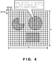
- Fig. 4 is a view showing an example of a case in which part of a three-dimensional layer-by-layer shaped object is included in the mesh model of the shaping plane on which the three-dimensional layer-by-layer shaped object is to be shaped by the three-dimensional layer-by-layer shaping apparatus 200 according to this embodiment.
- the three-dimensional layer-by-layer shaping apparatus 200 determines the defocus amounts and scanning rates by, for example, dividing the shaping plane into n ⁇ m square mesh elements which are assigned respective defocus amounts and scanning rates.
- the respective defocus amounts and scanning rates are determined in consideration, for example, of the presence or absence of part of the three-dimensional layer-by-layer shaped object 120 in respective mesh elements, which part will be included in the shaping plane along with the progress of the shaping. That is, dividing the shaping plane into mesh elements as shown in Fig. 3 enables the three-dimensional layer-by-layer shaping apparatus 200 to control the focus and scanning rate of the electron beam 130 per mesh element. This allows the three-dimensional layer-by-layer shaping apparatus 200 to, when performing preliminary sintering (preheating), keep the surface temperature of the shaping plane even, which can be achieved by decreasing the scanning rate in outer mesh elements and increasing the scanning rate in inner mesh elements.
- some mesh elements in the shaping plane may have their temperatures increased by the heat in the layer below it (lower layer). More specifically, the mesh elements in the upper layer, together with some mesh elements around them, may have their temperatures increased if the mesh elements are located above part of the three-dimensional layer-by-layer shaped object 120, which part has been melted and solidified in the lower layer.
- the temperature increase can be compensated for, as is the case with preliminarily sintering, by increasing the scanning rate in the mesh elements in the upper layer.
- the surface temperature of the shaping plane can be kept even.
- Fig. 5 is a flowchart explaining the procedure of the three-dimensional layer-by-layer shaping apparatus 200 according to this embodiment.
- the three-dimensional layer-by-layer shaping apparatus 200 acquires layer-by-layer shaping data (shaping model) of the three-dimensional layer-by-layer shaped object 120.
- the data may be input manually by its user, or acquired from CAM (Computer Aided Manufacturing) or CAD (Computer Aided Design).
- step S503 the three-dimensional layer-by-layer shaping apparatus 200 judges whether to execute preliminary sintering. If the judgment is to execute preliminary sintering (YES in step S503), the three-dimensional layer-by-layer shaping apparatus 200 advances to step S505. In step S505, the three-dimensional layer-by-layer shaping apparatus 200 generates the scanning data for scanning a preliminarily sintered region by the electron beam 130.
- step S503 the three-dimensional layer-by-layer shaping apparatus 200 advances to step S313.
- step S313 the three-dimensional layer-by-layer shaping apparatus 200 generates the scanning data for scanning a melted region by the electron beam 130.
- step S507 the three-dimensional layer-by-layer shaping apparatus 200 judges the defocus amount and scanning rate of the electron beam 130.
- step S509 the three-dimensional layer-by-layer shaping apparatus 200 executes preliminary sintering and melting using the determined defocus amount and scanning rate.
- step S311 the three-dimensional layer-by-layer shaping apparatus 200 judges whether the shaping of the three-dimensional layer-by-layer shaped object 120 has been completed. If the judgment is that the shaping has been completed (YES in step S311), the three-dimensional layer-by-layer shaping apparatus 200 terminates the process. If the judgment is that the shaping has not been completed (NO in step S311), the three-dimensional layer-by-layer shaping apparatus 200 repeats step S503 and the subsequent steps.
- This embodiment controls not only the defocus amount but also the scanning rate of the electron beam. Therefore this embodiment can, without using a blanking mechanism, fine-control the temperature of the shaping plane and thus can, when performing preliminary sintering (preheating), keep the temperature of the shaping plane even.
- FIG. 6 is a view explaining the configuration of the three-dimensional layer-by-layer shaping apparatus 600 according to this embodiment.
- This embodiment differs from the abovementioned second embodiment in that the three-dimensional layer-by-layer shaping apparatus 600, unlike the three-dimensional layer-by-layer shaping apparatus 200, includes a temperature measurement unit.
- the rest of the configuration and the operation are the same as those of the second embodiment, and thus the same reference numerals denote the same parts and same operations, and a detailed explanation thereof will be omitted.
- the three-dimensional layer-by-layer shaping apparatus 600 includes a temperature measurement unit 608.
- the temperature measurement unit 608 measures the temperature of the shaping plane, or more precisely the temperature of the material 150 on the shaping plane or of the top of the shaping table 140, and transmits data of the measured temperature to the controller 201. Based on the temperature data received, the controller 201 determines the defocus amount and scanning rate.
- the focus and scanning rate controls can be performed in more detail by feedbacking or feedforwarding the temperature data measured by the temperature measurement unit 608 to the controller 201.
- Examples of the temperature measurement unit 608 include, but are not limited to, a thermography or radiation thermometer.
- This embodiment measures the temperature of the shaping plane. By feedbacking or feedforwarding the measured temperature data to the controller, this embodiment can perform more detailed focus and scanning rate controls, and can thus control the temperature of the shaping plane more freely and shape three-dimensional layer-by-layer shaped objects with higher accuracy.
Landscapes
- Engineering & Computer Science (AREA)
- Chemical & Material Sciences (AREA)
- Materials Engineering (AREA)
- Manufacturing & Machinery (AREA)
- Mechanical Engineering (AREA)
- Physics & Mathematics (AREA)
- Analytical Chemistry (AREA)
- Optics & Photonics (AREA)
- Toxicology (AREA)
- Health & Medical Sciences (AREA)
- General Health & Medical Sciences (AREA)
- Plasma & Fusion (AREA)
- Automation & Control Theory (AREA)
- Powder Metallurgy (AREA)
Claims (6)
- Dreidimensionales Schicht-für-Schicht-Formgerät (100, 200, 600), mit:einer Materialverteilungseinrichtung (101), die dazu eingerichtet ist, um ein Material oder Materialien eines dreidimensionalen schichtweise geformten Objekts (120) auf einer Formungsplatte (140) zu verteilen, auf der das dreidimensionale schichtweise geformte Objekt (120) geformt werden soll;einer Elektronenkanone (102), die dazu eingerichtet ist, um einen Elektronenstrahl (130) zu erzeugen;mindestens einem Deflektor (103), der dazu eingerichtet ist, um den Elektronenstrahl (130) so abzulenken, dass der Elektronenstrahl (130) die Formungsplatte (140) ein- oder zweidimensional abtastet;mindestens einer Linse (104), die zwischen der Elektronenkanone (102) und dem Deflektor (103) angeordnet ist und dazu eingerichtet ist, um den Elektronenstrahl (130) so zu fokussieren, dass der Elektronenstrahl (130) einen Fokus auf der Formungsplatte (140) bildet;einer Fokussteuerungseinrichtung (105), die dazu eingerichtet ist, um den Fokus des Elektronenstrahls (130) auf der Grundlage dessen zu steuern, welches Gebiet durch den Elektronenstrahl (130) abzutasten ist; undeiner Steuerungseinrichtung (201), die dazu eingerichtet ist, um die Ablenkrichtung des Deflektors (103) und eine Abtastrate zu steuern,wobei das dreidimensionale Schicht-für-Schicht-Formgerät (100, 200, 600) ferner eine Temperaturmesseinheit (608) für die Formungsplatte (140) umfasst, wobei die Steuerungseinrichtung (201) dazu eingerichtet ist, um die Ablenkrichtung und die Abtastrate auf der Grundlage der Temperatur der Formungsplatte (140) zu steuern, und wobei die Fokussteuerungseinrichtung (105) dazu eingerichtet ist, um den Fokus auf der Grundlage der Temperatur der Formungsplatte (140) zu steuern, und dazu eingerichtet ist, um den Elektronenstrahl (130) zu defokussieren, falls das von dem Elektronenstrahl (130) abzutastende Gebiet ein nicht geschmolzenes Gebiet ist, in dem das Material nicht geschmolzen werden soll.
- Dreidimensionales Schicht-für-Schicht-Formgerät (100, 200, 600) nach Anspruch 1, wobei die Fokussteuerungseinrichtung (105) dazu eingerichtet ist, um den Elektronenstrahl (130) zu defokussieren, falls das durch den Elektronenstrahl (130) abzutastende Gebiet vorläufig gesintert werden soll.
- Dreidimensionales Schicht-für-Schicht-Formgerät (100, 200, 600) nach Anspruch 1 oder 2, wobei die Steuerungseinrichtung (201) dazu eingerichtet ist, um die Abtastrate für das nicht geschmolzene Gebiet höher als die für das geschmolzene Gebiet, in dem das Material geschmolzen werden soll, zu machen.
- Dreidimensionales Schicht-für-Schicht-Formgerät (100, 200, 600) nach einem der Ansprüche 1 bis 3, wobei die Fokussteuerungseinrichtung (105) dazu eingerichtet ist, um den Elektronenstrahl (130) zu defokussieren, falls die Ausgangsleistung des Elektronenstrahls (130) geändert wird.
- Dreidimensionales Schicht-für-Schicht-Formgerät (100, 200, 600) nach einem der Ansprüche 1 bis 4, wobei die Steuerungseinrichtung (201) dazu eingerichtet ist, um die Formungsplatte (140) in Gitterelemente zu unterteilen, und dazu eingerichtet ist, um die Abtastrate pro Gitterelement zu steuern.
- Steuerungsverfahren für ein dreidimensionales Schicht-für-Schicht-Formgerät, mit den Schritten:Verteilen eines Materials oder von Materialien eines dreidimensionalen schichtweise geformten Objekts (120) auf einer Formungsplatte (140), auf der das dreidimensionale schichtweise geformte Objekt (120) geformt werden soll;Erzeugen eines Elektronenstrahls (130);Veranlassen von mindestens einem Deflektor (103) den Elektronenstrahl (130) so abzulenken, dass der Elektronenstrahl (130) die Formungsplatte (140) ein- oder zweidimensional abtastet;Veranlassen von mindestens einer Linse (104), die zwischen der Elektronenkanone (102) und dem Deflektor (103) angeordnet ist, den Elektronenstrahl (130) so zu fokussieren, dass der Elektronenstrahl (130) einen Fokus auf der Formungsplatte (140) bildet;Steuern des Fokus des Elektronenstrahls (130) auf der Grundlage der Temperatur der Formungsplatte (140);Steuern der Ablenkrichtung des Deflektors (103) und der Abtastrate auf der Grundlage der Temperatur der Formungsplatte (140); undDefokussieren des Elektronenstrahls (130), wenn das durch den Elektronenstrahl (130) abzutastende Gebiet ein nicht geschmolzenes Gebiet ist, in dem das Material nicht geschmolzen werden soll.
Applications Claiming Priority (1)
| Application Number | Priority Date | Filing Date | Title |
|---|---|---|---|
| PCT/JP2016/059643 WO2017163403A1 (ja) | 2016-03-25 | 2016-03-25 | 3次元積層造形装置、3次元積層造形装置の制御方法および3次元積層造形装置の制御プログラム |
Publications (3)
| Publication Number | Publication Date |
|---|---|
| EP3243634A1 EP3243634A1 (de) | 2017-11-15 |
| EP3243634A4 EP3243634A4 (de) | 2018-06-20 |
| EP3243634B1 true EP3243634B1 (de) | 2020-12-23 |
Family
ID=59900133
Family Applications (1)
| Application Number | Title | Priority Date | Filing Date |
|---|---|---|---|
| EP16825688.1A Active EP3243634B1 (de) | 2016-03-25 | 2016-03-25 | Vorrichtung zur dreidimensionalen schichtweisen formung und steuerungsverfahren für vorrichtung zur dreidimensionalen schichtweisen formung |
Country Status (4)
| Country | Link |
|---|---|
| US (1) | US10566171B2 (de) |
| EP (1) | EP3243634B1 (de) |
| JP (1) | JP6273372B1 (de) |
| WO (1) | WO2017163403A1 (de) |
Families Citing this family (8)
| Publication number | Priority date | Publication date | Assignee | Title |
|---|---|---|---|---|
| WO2016103493A1 (ja) * | 2014-12-26 | 2016-06-30 | 技術研究組合次世代3D積層造形技術総合開発機構 | 3次元造形装置、3次元造形装置の制御方法および制御プログラム |
| CN111148588B (zh) * | 2017-10-06 | 2022-06-24 | 株式会社Ihi | 三维层叠造型物制造装置以及三维层叠造型物制造方法 |
| WO2019216228A1 (ja) * | 2018-05-09 | 2019-11-14 | 株式会社ニコン | 造形システム、及び、造形方法 |
| US11426818B2 (en) | 2018-08-10 | 2022-08-30 | The Research Foundation for the State University | Additive manufacturing processes and additively manufactured products |
| KR102130343B1 (ko) * | 2018-11-14 | 2020-08-06 | 한국기계연구원 | 레이저와 분말을 이용한 3차원 형상 제조장치 |
| US11763524B2 (en) * | 2019-09-13 | 2023-09-19 | Ansys, Inc. | Layered meshing for additive manufacturing simulations |
| CN111283196B (zh) * | 2020-03-05 | 2021-10-08 | 华中科技大学 | 铁基陶瓷复合材料薄壁回转体构件及其激光增材制造方法 |
| JP7378628B2 (ja) | 2020-07-31 | 2023-11-13 | 株式会社日立ハイテク | 電解質分析装置 |
Family Cites Families (11)
| Publication number | Priority date | Publication date | Assignee | Title |
|---|---|---|---|---|
| SE521124C2 (sv) * | 2000-04-27 | 2003-09-30 | Arcam Ab | Anordning samt metod för framställande av en tredimensionell produkt |
| JP4571558B2 (ja) | 2005-08-31 | 2010-10-27 | 日本電子株式会社 | 荷電粒子ビーム露光装置の調整方法及び荷電粒子ビーム露光装置 |
| KR102182567B1 (ko) | 2011-12-28 | 2020-11-24 | 아르켐 에이비 | 첨가적으로 제조되는 3차원 물품들의 레졸루션을 증가시키기 위한 방법 및 장치 |
| US9064671B2 (en) | 2012-05-09 | 2015-06-23 | Arcam Ab | Method and apparatus for generating electron beams |
| DE102013017792A1 (de) | 2013-10-28 | 2015-04-30 | Cl Schutzrechtsverwaltungs Gmbh | Verfahren zum Herstellen eines dreidimensionalen Bauteils |
| US9789563B2 (en) * | 2013-12-20 | 2017-10-17 | Arcam Ab | Method for additive manufacturing |
| JP2015168877A (ja) | 2014-03-10 | 2015-09-28 | 日本電子株式会社 | 3次元積層造形装置及び3次元積層造形方法 |
| JP2015193866A (ja) * | 2014-03-31 | 2015-11-05 | 日本電子株式会社 | 3次元積層造形装置、3次元積層造形システム及び3次元積層造形方法 |
| US20150283613A1 (en) | 2014-04-02 | 2015-10-08 | Arcam Ab | Method for fusing a workpiece |
| JP6092465B1 (ja) | 2015-12-07 | 2017-03-08 | 技術研究組合次世代3D積層造形技術総合開発機構 | 3次元造形装置、3次元造形装置の制御方法および3次元造形装置の制御プログラム |
| EP3223299A4 (de) | 2016-01-21 | 2018-04-18 | Technology Research Association for Future Additive Manufacturing | Vorrichtung zur 3d-modellierung, steuerungsverfahren für vorrichtung zur 3d-modellierung und steuerungsprogramm für vorrichtung zur 3d-modellierung |
-
2016
- 2016-03-25 JP JP2016547102A patent/JP6273372B1/ja active Active
- 2016-03-25 EP EP16825688.1A patent/EP3243634B1/de active Active
- 2016-03-25 WO PCT/JP2016/059643 patent/WO2017163403A1/ja active Application Filing
- 2016-03-25 US US15/123,350 patent/US10566171B2/en active Active
Non-Patent Citations (1)
| Title |
|---|
| None * |
Also Published As
| Publication number | Publication date |
|---|---|
| US20180166251A1 (en) | 2018-06-14 |
| EP3243634A4 (de) | 2018-06-20 |
| WO2017163403A1 (ja) | 2017-09-28 |
| JP6273372B1 (ja) | 2018-01-31 |
| JPWO2017163403A1 (ja) | 2018-03-29 |
| EP3243634A1 (de) | 2017-11-15 |
| US10566171B2 (en) | 2020-02-18 |
Similar Documents
| Publication | Publication Date | Title |
|---|---|---|
| EP3243634B1 (de) | Vorrichtung zur dreidimensionalen schichtweisen formung und steuerungsverfahren für vorrichtung zur dreidimensionalen schichtweisen formung | |
| JP6771076B2 (ja) | 三次元の部材の生成的な製造の為の装置 | |
| US10603748B2 (en) | Production of a component by selective laser melting | |
| JP5108884B2 (ja) | 3次元物体を生成する方法および装置 | |
| US10399146B2 (en) | Contour scanning for additive manufacturing process | |
| US20150306820A1 (en) | Method for melting powder, comprising heating of the area adjacent to the bath | |
| US20170304895A1 (en) | Additive manufacturing apparatus and method | |
| JP5452072B2 (ja) | 電子ビーム造形方法 | |
| RU2450891C1 (ru) | Способ спекания деталей лазерным послойным синтезом | |
| EP3059031B1 (de) | Vorrichtung für dreidimensionales drucken , steuerungsverfahren für die vorrichtung für dreidimensionales drucken und steuerungsprogramm | |
| JP6600278B2 (ja) | 選択型ビーム積層造形装置及び選択型ビーム積層造形方法 | |
| US20200376556A1 (en) | Additive manufacturing method with controlled solidification and corresponding device | |
| US11014189B2 (en) | Method to control additive manufacturing builds using laser angle of incidence | |
| Shkoruta et al. | Iterative learning control for power profile shaping in selective laser melting | |
| JP7302145B2 (ja) | スポット予熱 | |
| CN109982792A (zh) | 用于生产单晶工件的方法、用途和设备 | |
| CN108068342B (zh) | 用于生产三维工件的设备和操作该设备的方法 | |
| CN108421974B (zh) | 包括加热系统的用于生产三维工件的设备 | |
| CN110621479A (zh) | 用于增材制造的不断变化的影线 | |
| CN110621425A (zh) | 用于增材制造的三角形影线图案 | |
| WO2018109943A1 (ja) | 3次元造形装置、3次元造形装置の制御方法および3次元造形装置の制御プログラム | |
| RU165868U1 (ru) | Устройство для получения изделий из порошковых материалов | |
| CN110573278A (zh) | 用于影线图案的直角边消除策略 | |
| US10882135B2 (en) | Apparatus for additively manufacturing of three-dimensional objects | |
| EP3461574A1 (de) | Modifizierter rahmen und wiederbeschichtungssystem |
Legal Events
| Date | Code | Title | Description |
|---|---|---|---|
| STAA | Information on the status of an ep patent application or granted ep patent |
Free format text: STATUS: UNKNOWN |
|
| STAA | Information on the status of an ep patent application or granted ep patent |
Free format text: STATUS: THE INTERNATIONAL PUBLICATION HAS BEEN MADE |
|
| PUAI | Public reference made under article 153(3) epc to a published international application that has entered the european phase |
Free format text: ORIGINAL CODE: 0009012 |
|
| STAA | Information on the status of an ep patent application or granted ep patent |
Free format text: STATUS: REQUEST FOR EXAMINATION WAS MADE |
|
| 17P | Request for examination filed |
Effective date: 20170123 |
|
| AK | Designated contracting states |
Kind code of ref document: A1 Designated state(s): AL AT BE BG CH CY CZ DE DK EE ES FI FR GB GR HR HU IE IS IT LI LT LU LV MC MK MT NL NO PL PT RO RS SE SI SK SM TR |
|
| AX | Request for extension of the european patent |
Extension state: BA ME |
|
| RIN1 | Information on inventor provided before grant (corrected) |
Inventor name: MORIMURA TOSHIYUKI Inventor name: GOTO KAZUYA Inventor name: YUAN ZHIXIONG Inventor name: SHIMBO TAKAHIRO |
|
| R17P | Request for examination filed (corrected) |
Effective date: 20170123 |
|
| A4 | Supplementary search report drawn up and despatched |
Effective date: 20180518 |
|
| RIC1 | Information provided on ipc code assigned before grant |
Ipc: B23K 15/00 20060101ALN20180514BHEP Ipc: B33Y 30/00 20150101ALI20180514BHEP Ipc: H01J 37/21 20060101ALN20180514BHEP Ipc: H01J 37/302 20060101ALN20180514BHEP Ipc: B33Y 10/00 20150101ALI20180514BHEP Ipc: H01J 37/317 20060101ALN20180514BHEP Ipc: B29C 67/00 20170101AFI20180514BHEP Ipc: B22F 3/105 20060101ALI20180514BHEP Ipc: G21K 1/08 20060101ALN20180514BHEP |
|
| DAV | Request for validation of the european patent (deleted) | ||
| DAX | Request for extension of the european patent (deleted) | ||
| STAA | Information on the status of an ep patent application or granted ep patent |
Free format text: STATUS: EXAMINATION IS IN PROGRESS |
|
| 17Q | First examination report despatched |
Effective date: 20191203 |
|
| RIC1 | Information provided on ipc code assigned before grant |
Ipc: H01J 37/305 20060101ALI20200623BHEP Ipc: H01J 37/21 20060101ALN20200623BHEP Ipc: B22F 3/105 20060101ALI20200623BHEP Ipc: B23K 15/00 20060101ALN20200623BHEP Ipc: H01J 37/302 20060101ALN20200623BHEP Ipc: H01J 37/317 20060101ALN20200623BHEP Ipc: B29C 67/00 20170101AFI20200623BHEP Ipc: B33Y 30/00 20150101ALI20200623BHEP Ipc: B33Y 10/00 20150101ALI20200623BHEP Ipc: G21K 1/08 20060101ALN20200623BHEP |
|
| REG | Reference to a national code |
Ref country code: DE Ref legal event code: R079 Ref document number: 602016050340 Country of ref document: DE Free format text: PREVIOUS MAIN CLASS: B29C0067000000 Ipc: B22F0003105000 |
|
| RIC1 | Information provided on ipc code assigned before grant |
Ipc: B22F 3/105 20060101AFI20200710BHEP Ipc: B29C 64/20 20170101ALN20200710BHEP Ipc: G21K 1/08 20060101ALN20200710BHEP Ipc: H01J 37/302 20060101ALI20200710BHEP Ipc: B23K 15/00 20060101ALI20200710BHEP Ipc: H01J 37/305 20060101ALI20200710BHEP Ipc: B29C 64/10 20170101ALN20200710BHEP Ipc: B29C 67/00 20170101ALN20200710BHEP Ipc: H01J 37/21 20060101ALI20200710BHEP Ipc: B33Y 10/00 20150101ALI20200710BHEP Ipc: B33Y 30/00 20150101ALI20200710BHEP |
|
| GRAP | Despatch of communication of intention to grant a patent |
Free format text: ORIGINAL CODE: EPIDOSNIGR1 |
|
| STAA | Information on the status of an ep patent application or granted ep patent |
Free format text: STATUS: GRANT OF PATENT IS INTENDED |
|
| RIC1 | Information provided on ipc code assigned before grant |
Ipc: B33Y 10/00 20150101ALI20200803BHEP Ipc: H01J 37/302 20060101ALI20200803BHEP Ipc: B29C 64/20 20170101ALN20200803BHEP Ipc: B22F 3/105 20060101AFI20200803BHEP Ipc: B23K 15/00 20060101ALI20200803BHEP Ipc: G21K 1/08 20060101ALN20200803BHEP Ipc: B29C 67/00 20170101ALN20200803BHEP Ipc: B33Y 30/00 20150101ALI20200803BHEP Ipc: H01J 37/305 20060101ALI20200803BHEP Ipc: H01J 37/21 20060101ALI20200803BHEP Ipc: B29C 64/10 20170101ALN20200803BHEP |
|
| INTG | Intention to grant announced |
Effective date: 20200902 |
|
| GRAS | Grant fee paid |
Free format text: ORIGINAL CODE: EPIDOSNIGR3 |
|
| GRAA | (expected) grant |
Free format text: ORIGINAL CODE: 0009210 |
|
| STAA | Information on the status of an ep patent application or granted ep patent |
Free format text: STATUS: THE PATENT HAS BEEN GRANTED |
|
| AK | Designated contracting states |
Kind code of ref document: B1 Designated state(s): AL AT BE BG CH CY CZ DE DK EE ES FI FR GB GR HR HU IE IS IT LI LT LU LV MC MK MT NL NO PL PT RO RS SE SI SK SM TR |
|
| REG | Reference to a national code |
Ref country code: GB Ref legal event code: FG4D |
|
| REG | Reference to a national code |
Ref country code: SE Ref legal event code: TRGR |
|
| REG | Reference to a national code |
Ref country code: DE Ref legal event code: R096 Ref document number: 602016050340 Country of ref document: DE |
|
| REG | Reference to a national code |
Ref country code: AT Ref legal event code: REF Ref document number: 1347253 Country of ref document: AT Kind code of ref document: T Effective date: 20210115 |
|
| REG | Reference to a national code |
Ref country code: IE Ref legal event code: FG4D |
|
| PG25 | Lapsed in a contracting state [announced via postgrant information from national office to epo] |
Ref country code: NO Free format text: LAPSE BECAUSE OF FAILURE TO SUBMIT A TRANSLATION OF THE DESCRIPTION OR TO PAY THE FEE WITHIN THE PRESCRIBED TIME-LIMIT Effective date: 20210323 Ref country code: RS Free format text: LAPSE BECAUSE OF FAILURE TO SUBMIT A TRANSLATION OF THE DESCRIPTION OR TO PAY THE FEE WITHIN THE PRESCRIBED TIME-LIMIT Effective date: 20201223 Ref country code: FI Free format text: LAPSE BECAUSE OF FAILURE TO SUBMIT A TRANSLATION OF THE DESCRIPTION OR TO PAY THE FEE WITHIN THE PRESCRIBED TIME-LIMIT Effective date: 20201223 Ref country code: GR Free format text: LAPSE BECAUSE OF FAILURE TO SUBMIT A TRANSLATION OF THE DESCRIPTION OR TO PAY THE FEE WITHIN THE PRESCRIBED TIME-LIMIT Effective date: 20210324 |
|
| REG | Reference to a national code |
Ref country code: AT Ref legal event code: MK05 Ref document number: 1347253 Country of ref document: AT Kind code of ref document: T Effective date: 20201223 |
|
| REG | Reference to a national code |
Ref country code: NL Ref legal event code: MP Effective date: 20201223 |
|
| PG25 | Lapsed in a contracting state [announced via postgrant information from national office to epo] |
Ref country code: BG Free format text: LAPSE BECAUSE OF FAILURE TO SUBMIT A TRANSLATION OF THE DESCRIPTION OR TO PAY THE FEE WITHIN THE PRESCRIBED TIME-LIMIT Effective date: 20210323 Ref country code: LV Free format text: LAPSE BECAUSE OF FAILURE TO SUBMIT A TRANSLATION OF THE DESCRIPTION OR TO PAY THE FEE WITHIN THE PRESCRIBED TIME-LIMIT Effective date: 20201223 |
|
| PG25 | Lapsed in a contracting state [announced via postgrant information from national office to epo] |
Ref country code: HR Free format text: LAPSE BECAUSE OF FAILURE TO SUBMIT A TRANSLATION OF THE DESCRIPTION OR TO PAY THE FEE WITHIN THE PRESCRIBED TIME-LIMIT Effective date: 20201223 Ref country code: NL Free format text: LAPSE BECAUSE OF FAILURE TO SUBMIT A TRANSLATION OF THE DESCRIPTION OR TO PAY THE FEE WITHIN THE PRESCRIBED TIME-LIMIT Effective date: 20201223 |
|
| REG | Reference to a national code |
Ref country code: LT Ref legal event code: MG9D |
|
| PG25 | Lapsed in a contracting state [announced via postgrant information from national office to epo] |
Ref country code: CZ Free format text: LAPSE BECAUSE OF FAILURE TO SUBMIT A TRANSLATION OF THE DESCRIPTION OR TO PAY THE FEE WITHIN THE PRESCRIBED TIME-LIMIT Effective date: 20201223 Ref country code: EE Free format text: LAPSE BECAUSE OF FAILURE TO SUBMIT A TRANSLATION OF THE DESCRIPTION OR TO PAY THE FEE WITHIN THE PRESCRIBED TIME-LIMIT Effective date: 20201223 Ref country code: SM Free format text: LAPSE BECAUSE OF FAILURE TO SUBMIT A TRANSLATION OF THE DESCRIPTION OR TO PAY THE FEE WITHIN THE PRESCRIBED TIME-LIMIT Effective date: 20201223 Ref country code: LT Free format text: LAPSE BECAUSE OF FAILURE TO SUBMIT A TRANSLATION OF THE DESCRIPTION OR TO PAY THE FEE WITHIN THE PRESCRIBED TIME-LIMIT Effective date: 20201223 Ref country code: RO Free format text: LAPSE BECAUSE OF FAILURE TO SUBMIT A TRANSLATION OF THE DESCRIPTION OR TO PAY THE FEE WITHIN THE PRESCRIBED TIME-LIMIT Effective date: 20201223 Ref country code: PT Free format text: LAPSE BECAUSE OF FAILURE TO SUBMIT A TRANSLATION OF THE DESCRIPTION OR TO PAY THE FEE WITHIN THE PRESCRIBED TIME-LIMIT Effective date: 20210423 Ref country code: SK Free format text: LAPSE BECAUSE OF FAILURE TO SUBMIT A TRANSLATION OF THE DESCRIPTION OR TO PAY THE FEE WITHIN THE PRESCRIBED TIME-LIMIT Effective date: 20201223 |
|
| PG25 | Lapsed in a contracting state [announced via postgrant information from national office to epo] |
Ref country code: AT Free format text: LAPSE BECAUSE OF FAILURE TO SUBMIT A TRANSLATION OF THE DESCRIPTION OR TO PAY THE FEE WITHIN THE PRESCRIBED TIME-LIMIT Effective date: 20201223 Ref country code: PL Free format text: LAPSE BECAUSE OF FAILURE TO SUBMIT A TRANSLATION OF THE DESCRIPTION OR TO PAY THE FEE WITHIN THE PRESCRIBED TIME-LIMIT Effective date: 20201223 |
|
| REG | Reference to a national code |
Ref country code: DE Ref legal event code: R097 Ref document number: 602016050340 Country of ref document: DE |
|
| PG25 | Lapsed in a contracting state [announced via postgrant information from national office to epo] |
Ref country code: IS Free format text: LAPSE BECAUSE OF FAILURE TO SUBMIT A TRANSLATION OF THE DESCRIPTION OR TO PAY THE FEE WITHIN THE PRESCRIBED TIME-LIMIT Effective date: 20210423 |
|
| PG25 | Lapsed in a contracting state [announced via postgrant information from national office to epo] |
Ref country code: AL Free format text: LAPSE BECAUSE OF FAILURE TO SUBMIT A TRANSLATION OF THE DESCRIPTION OR TO PAY THE FEE WITHIN THE PRESCRIBED TIME-LIMIT Effective date: 20201223 Ref country code: IT Free format text: LAPSE BECAUSE OF FAILURE TO SUBMIT A TRANSLATION OF THE DESCRIPTION OR TO PAY THE FEE WITHIN THE PRESCRIBED TIME-LIMIT Effective date: 20201223 Ref country code: MC Free format text: LAPSE BECAUSE OF FAILURE TO SUBMIT A TRANSLATION OF THE DESCRIPTION OR TO PAY THE FEE WITHIN THE PRESCRIBED TIME-LIMIT Effective date: 20201223 |
|
| PLBE | No opposition filed within time limit |
Free format text: ORIGINAL CODE: 0009261 |
|
| REG | Reference to a national code |
Ref country code: CH Ref legal event code: PL |
|
| STAA | Information on the status of an ep patent application or granted ep patent |
Free format text: STATUS: NO OPPOSITION FILED WITHIN TIME LIMIT |
|
| PG25 | Lapsed in a contracting state [announced via postgrant information from national office to epo] |
Ref country code: DK Free format text: LAPSE BECAUSE OF FAILURE TO SUBMIT A TRANSLATION OF THE DESCRIPTION OR TO PAY THE FEE WITHIN THE PRESCRIBED TIME-LIMIT Effective date: 20201223 |
|
| 26N | No opposition filed |
Effective date: 20210924 |
|
| REG | Reference to a national code |
Ref country code: BE Ref legal event code: MM Effective date: 20210331 |
|
| REG | Reference to a national code |
Ref country code: DE Ref legal event code: R081 Ref document number: 602016050340 Country of ref document: DE Owner name: JEOL LTD., AKISHIMA-SHI, JP Free format text: FORMER OWNER: TECHNOLOGY RESEARCH ASSOCIATION FOR FUTURE ADDITIVE MANUFACTURING, TOKYO, JP |
|
| PG25 | Lapsed in a contracting state [announced via postgrant information from national office to epo] |
Ref country code: FR Free format text: LAPSE BECAUSE OF NON-PAYMENT OF DUE FEES Effective date: 20210331 Ref country code: IE Free format text: LAPSE BECAUSE OF NON-PAYMENT OF DUE FEES Effective date: 20210325 Ref country code: ES Free format text: LAPSE BECAUSE OF FAILURE TO SUBMIT A TRANSLATION OF THE DESCRIPTION OR TO PAY THE FEE WITHIN THE PRESCRIBED TIME-LIMIT Effective date: 20201223 Ref country code: LI Free format text: LAPSE BECAUSE OF NON-PAYMENT OF DUE FEES Effective date: 20210331 Ref country code: LU Free format text: LAPSE BECAUSE OF NON-PAYMENT OF DUE FEES Effective date: 20210325 Ref country code: CH Free format text: LAPSE BECAUSE OF NON-PAYMENT OF DUE FEES Effective date: 20210331 |
|
| REG | Reference to a national code |
Ref country code: GB Ref legal event code: 732E Free format text: REGISTERED BETWEEN 20220106 AND 20220112 |
|
| PG25 | Lapsed in a contracting state [announced via postgrant information from national office to epo] |
Ref country code: SI Free format text: LAPSE BECAUSE OF FAILURE TO SUBMIT A TRANSLATION OF THE DESCRIPTION OR TO PAY THE FEE WITHIN THE PRESCRIBED TIME-LIMIT Effective date: 20201223 |
|
| PG25 | Lapsed in a contracting state [announced via postgrant information from national office to epo] |
Ref country code: IS Free format text: LAPSE BECAUSE OF FAILURE TO SUBMIT A TRANSLATION OF THE DESCRIPTION OR TO PAY THE FEE WITHIN THE PRESCRIBED TIME-LIMIT Effective date: 20210423 |
|
| PG25 | Lapsed in a contracting state [announced via postgrant information from national office to epo] |
Ref country code: BE Free format text: LAPSE BECAUSE OF NON-PAYMENT OF DUE FEES Effective date: 20210331 |
|
| PG25 | Lapsed in a contracting state [announced via postgrant information from national office to epo] |
Ref country code: HU Free format text: LAPSE BECAUSE OF FAILURE TO SUBMIT A TRANSLATION OF THE DESCRIPTION OR TO PAY THE FEE WITHIN THE PRESCRIBED TIME-LIMIT; INVALID AB INITIO Effective date: 20160325 |
|
| PGFP | Annual fee paid to national office [announced via postgrant information from national office to epo] |
Ref country code: SE Payment date: 20230314 Year of fee payment: 8 |
|
| PG25 | Lapsed in a contracting state [announced via postgrant information from national office to epo] |
Ref country code: CY Free format text: LAPSE BECAUSE OF FAILURE TO SUBMIT A TRANSLATION OF THE DESCRIPTION OR TO PAY THE FEE WITHIN THE PRESCRIBED TIME-LIMIT Effective date: 20201223 |
|
| PG25 | Lapsed in a contracting state [announced via postgrant information from national office to epo] |
Ref country code: MK Free format text: LAPSE BECAUSE OF FAILURE TO SUBMIT A TRANSLATION OF THE DESCRIPTION OR TO PAY THE FEE WITHIN THE PRESCRIBED TIME-LIMIT Effective date: 20201223 |
|
| PGFP | Annual fee paid to national office [announced via postgrant information from national office to epo] |
Ref country code: DE Payment date: 20240320 Year of fee payment: 9 Ref country code: GB Payment date: 20240320 Year of fee payment: 9 |