EP3223322A1 - Light emitting device package - Google Patents
Light emitting device package Download PDFInfo
- Publication number
- EP3223322A1 EP3223322A1 EP17162253.3A EP17162253A EP3223322A1 EP 3223322 A1 EP3223322 A1 EP 3223322A1 EP 17162253 A EP17162253 A EP 17162253A EP 3223322 A1 EP3223322 A1 EP 3223322A1
- Authority
- EP
- European Patent Office
- Prior art keywords
- light emitting
- parts
- frame
- emitting device
- cavity
- Prior art date
- Legal status (The legal status is an assumption and is not a legal conclusion. Google has not performed a legal analysis and makes no representation as to the accuracy of the status listed.)
- Granted
Links
Images




Classifications
-
- H—ELECTRICITY
- H10—SEMICONDUCTOR DEVICES; ELECTRIC SOLID-STATE DEVICES NOT OTHERWISE PROVIDED FOR
- H10H—INORGANIC LIGHT-EMITTING SEMICONDUCTOR DEVICES HAVING POTENTIAL BARRIERS
- H10H20/00—Individual inorganic light-emitting semiconductor devices having potential barriers, e.g. light-emitting diodes [LED]
- H10H20/80—Constructional details
- H10H20/85—Packages
- H10H20/855—Optical field-shaping means, e.g. lenses
- H10H20/856—Reflecting means
-
- H—ELECTRICITY
- H10—SEMICONDUCTOR DEVICES; ELECTRIC SOLID-STATE DEVICES NOT OTHERWISE PROVIDED FOR
- H10D—INORGANIC ELECTRIC SEMICONDUCTOR DEVICES
- H10D8/00—Diodes
- H10D8/20—Breakdown diodes, e.g. avalanche diodes
- H10D8/25—Zener diodes
-
- H—ELECTRICITY
- H10—SEMICONDUCTOR DEVICES; ELECTRIC SOLID-STATE DEVICES NOT OTHERWISE PROVIDED FOR
- H10D—INORGANIC ELECTRIC SEMICONDUCTOR DEVICES
- H10D89/00—Aspects of integrated devices not covered by groups H10D84/00 - H10D88/00
- H10D89/60—Integrated devices comprising arrangements for electrical or thermal protection, e.g. protection circuits against electrostatic discharge [ESD]
-
- H—ELECTRICITY
- H10—SEMICONDUCTOR DEVICES; ELECTRIC SOLID-STATE DEVICES NOT OTHERWISE PROVIDED FOR
- H10H—INORGANIC LIGHT-EMITTING SEMICONDUCTOR DEVICES HAVING POTENTIAL BARRIERS
- H10H20/00—Individual inorganic light-emitting semiconductor devices having potential barriers, e.g. light-emitting diodes [LED]
- H10H20/80—Constructional details
- H10H20/85—Packages
- H10H20/8506—Containers
-
- H—ELECTRICITY
- H10—SEMICONDUCTOR DEVICES; ELECTRIC SOLID-STATE DEVICES NOT OTHERWISE PROVIDED FOR
- H10H—INORGANIC LIGHT-EMITTING SEMICONDUCTOR DEVICES HAVING POTENTIAL BARRIERS
- H10H20/00—Individual inorganic light-emitting semiconductor devices having potential barriers, e.g. light-emitting diodes [LED]
- H10H20/80—Constructional details
- H10H20/85—Packages
- H10H20/852—Encapsulations
- H10H20/853—Encapsulations characterised by their shape
-
- H—ELECTRICITY
- H10—SEMICONDUCTOR DEVICES; ELECTRIC SOLID-STATE DEVICES NOT OTHERWISE PROVIDED FOR
- H10H—INORGANIC LIGHT-EMITTING SEMICONDUCTOR DEVICES HAVING POTENTIAL BARRIERS
- H10H20/00—Individual inorganic light-emitting semiconductor devices having potential barriers, e.g. light-emitting diodes [LED]
- H10H20/80—Constructional details
- H10H20/85—Packages
- H10H20/857—Interconnections, e.g. lead-frames, bond wires or solder balls
-
- H—ELECTRICITY
- H10—SEMICONDUCTOR DEVICES; ELECTRIC SOLID-STATE DEVICES NOT OTHERWISE PROVIDED FOR
- H10H—INORGANIC LIGHT-EMITTING SEMICONDUCTOR DEVICES HAVING POTENTIAL BARRIERS
- H10H20/00—Individual inorganic light-emitting semiconductor devices having potential barriers, e.g. light-emitting diodes [LED]
- H10H20/80—Constructional details
- H10H20/85—Packages
- H10H20/858—Means for heat extraction or cooling
- H10H20/8585—Means for heat extraction or cooling being an interconnection
-
- H—ELECTRICITY
- H10—SEMICONDUCTOR DEVICES; ELECTRIC SOLID-STATE DEVICES NOT OTHERWISE PROVIDED FOR
- H10W—GENERIC PACKAGES, INTERCONNECTIONS, CONNECTORS OR OTHER CONSTRUCTIONAL DETAILS OF DEVICES COVERED BY CLASS H10
- H10W90/00—Package configurations
-
- H—ELECTRICITY
- H10—SEMICONDUCTOR DEVICES; ELECTRIC SOLID-STATE DEVICES NOT OTHERWISE PROVIDED FOR
- H10H—INORGANIC LIGHT-EMITTING SEMICONDUCTOR DEVICES HAVING POTENTIAL BARRIERS
- H10H20/00—Individual inorganic light-emitting semiconductor devices having potential barriers, e.g. light-emitting diodes [LED]
- H10H20/01—Manufacture or treatment
- H10H20/036—Manufacture or treatment of packages
- H10H20/0363—Manufacture or treatment of packages of optical field-shaping means
-
- H—ELECTRICITY
- H10—SEMICONDUCTOR DEVICES; ELECTRIC SOLID-STATE DEVICES NOT OTHERWISE PROVIDED FOR
- H10H—INORGANIC LIGHT-EMITTING SEMICONDUCTOR DEVICES HAVING POTENTIAL BARRIERS
- H10H20/00—Individual inorganic light-emitting semiconductor devices having potential barriers, e.g. light-emitting diodes [LED]
- H10H20/80—Constructional details
- H10H20/85—Packages
- H10H20/858—Means for heat extraction or cooling
- H10H20/8582—Means for heat extraction or cooling characterised by their shape
-
- H—ELECTRICITY
- H10—SEMICONDUCTOR DEVICES; ELECTRIC SOLID-STATE DEVICES NOT OTHERWISE PROVIDED FOR
- H10W—GENERIC PACKAGES, INTERCONNECTIONS, CONNECTORS OR OTHER CONSTRUCTIONAL DETAILS OF DEVICES COVERED BY CLASS H10
- H10W90/00—Package configurations
- H10W90/701—Package configurations characterised by the relative positions of pads or connectors relative to package parts
- H10W90/751—Package configurations characterised by the relative positions of pads or connectors relative to package parts of bond wires
- H10W90/753—Package configurations characterised by the relative positions of pads or connectors relative to package parts of bond wires between laterally-adjacent chips
Definitions
- the embodiment relates to a light emitting device package and a lighting device having the same.
- a light emitting diode includes a P-N junction diode having a characteristic of converting electrical energy into light energy.
- the light emitting device may be fabricated with compound semiconductors belonging to group III and V on the periodic table.
- the light-emitting device can produce various colors by adjusting the compositional ratio of the compound semiconductors.
- a nitride semiconductor represents superior thermal stability and wide bandgap energy so that the nitride semiconductor has been spotlighted in the field of optical devices and high-power electronic devices.
- blue light emitting devices, green light emitting devices, ultraviolet (UV) light emitting devices, and the like using nitride semiconductors are commercialized and widely used.
- the light emitting diode has been applied to various devices such as a backlight unit of a liquid crystal display, an electric signboard, an indicator, and a home appliance.
- the embodiment provides a light emitting device package, capable of improving light extraction efficiency, and a lighting device having the same.
- the embodiment provides a light emitting device package, capable of improving coupling force between components, and a lighting device having the same.
- the embodiment provides a chip-on-board (COB) light emitting device package having a stabile structure and a lighting device having the same.
- COB chip-on-board
- the light emitting device package includes a frame, a first lead frame spaced apart from the frame by a specific distance, a second lead frame spaced apart from the frame by the specific distance, a body coupled to the frame and the first and second lead frames and having a first cavity, and a plurality of light emitting devices provided on the frame exposed through the first cavity, in which the body includes a reflective part which is provided inside the first cavity to surround at least one of the light emitting devices, thereby improving light extraction efficiency.
- the deformation of the light emitting device package resulting from the contraction and the expansion of the light emitting device package can be prevented by the reflective part.
- the deformation of a molding part resulting from the contraction and the expansion of the molding part provided in the first cavity can be prevented by the reflective part.
- the deformation of the molding part can be prevented, thereby preventing the damage to a wire resulting from the deformation of the molding part.
- a lighting device may include the light emitting device package.
- the deformation of the light emitting device package resulting from the contraction and the expansion of the light emitting device package can be prevented by the reflective part extending across the central area of the cavity in which the light emitting devices are mounted.
- the deformation of the molding part resulting from the contraction and the expansion of the molding part provided in the first cavity can be prevented by the reflective part extending across the central area of the cavity in which the light emitting devices are mounted.
- the deformation of the molding part can be prevented, thereby preventing the damage to the wire resulting from the deformation of the molding part.
- the coupling force between the heat sinking plate and the body can be improved, and the external moisture can be prevented from being permeated due to the stepped structure.
- the stepped parts are provided on the lower portions of the first and second lead frames and supported by a mold frame to prevent the first and second lead frames from being deformed.
- the external moisture can be prevented from being permeated due to the stepped structures formed on the lower portion of the first and second lead frames.
- flexure structures are provided at edges of the first and second lead frames only to improve the coupling force with the body, but also to prevent a peripheral portion of the spacer, which is provided between the first and second frames, from being cracked.
- the protective part which covers the outer portion of the pad, is included to protect the pad and to improve the coupling force between the body and the first and second lead frames.
- at least one through hole is formed through the pad to improve the coupling force between the body and the first and second lead frames.
- a semiconductor device may include various electronic devices such as a light emitting device, a light receiving device, and the like.
- the light emitting device and the light receiving device may include a first conductive type semiconductor layer, an active layer, and a second conductive type semiconductor layer.
- the semiconductor device may be the light emitting device.
- the light emitting device emits light through the recombination between electrons and holes, and the wavelength of the light is determined depending on the intrinsic energy band gap of the material. Accordingly, the emitted light may be varied with the composition of the material.
- FIG. 1 is a perspective view showing a light emitting device package according to the embodiment.
- FIG. 2 is a sectional view showing the light emitting device package according to the embodiment.
- FIG. 3 is a plan view showing the light emitting device package according to the embodiment.
- FIG. 4 is a plan view showing a reflective part according to the embodiment.
- FIG. 5 is a plan view showing the reflective part and a first coupling part according to the embodiment.
- the light emitting device package 100 may include a frame (heat sinking plate) 110, a first lead frame 120, a second lead frame 130, a body 170, a protective device 160, and a plurality of light emitting devices 150.
- the protective device 160 and the light emitting devices 150 may be mounted on the frame 110.
- the first and second lead frames 120 and 130 may be spaced apart from the frame 110 by a specific distance.
- the light emitting device package 100 may be a chip-on-board (COB) light emitting device package.
- COB chip-on-board
- the light emitting device package 100 may be directly die-bonded onto a substrate and electrically connected with the substrate through a wire, but the embodiment is not limited thereto.
- the body 170 may include at least one of a transmissive material, a reflective material, and an insulating material.
- the body 170 may include a material having a reflectance higher than transmittance with respect to light emitted from the light emitting devices 150.
- the body 170 may include a resin-based insulating material.
- the body 170 may include at least one of a resin material, such as polyphthalamide (PPA), epoxy, or a silicone material, silicon (Si), a metallic material, photo sensitive glass (PSG), sapphire (Al2O3), and a printed circuit board (PCB).
- the body 170 may include four corners.
- the body 170 may include first and second corners 170a and 170b facing each other in a first direction X-X' and third and fourth corners 170c and 170d facing each other in a second direction Y-Y' perpendicular to the first direction X-X'.
- a first pad 121 of the first lead frame 120 may be exposed through the first corner 170a.
- a second pad 131 of the second lead frame 130 may be exposed through the second corner 170b.
- the first and second corners 170a and 170b may expose top surfaces of the first and second pads 121 and 131. End portions of the first and second corners 170a and 170b may cover edges of the first and second pads 121 and 131, respectively.
- first and second corners 170a and 170b may be provided outward from the first and second pads 121 and 131, respectively.
- the third and fourth corners 170c and 170d may be engaged with screws when the substrate (not shown) is coupled to the light emitting device package 100.
- the third and fourth corners 170c and 170d may be formed in curved structures such that the screws may be coupled to the third and fourth corners 170c and 170d, but the embodiment is not limited thereto.
- the third and fourth corners 170c and 170d may be formed in the curved structures having concave outer portions.
- the body 170 may be coupled to the frame 110, and the first and second lead frames 120 and 130.
- the body 170 may include a first cavity 171 a and a second cavity 171 b which expose portions of top surfaces of the frame 110 and the first and second lead frames 120 and 130.
- the first cavity 171 a may extend from the central area of the body 170.
- the first cavity 171 a may be provided in an area on which the light emitting devices 150 are mounted.
- the first cavity 171a may have a circular shape when viewed from a top view, but the embodiment is not limited thereto.
- the first cavity 171a may have an oval shape or at least three polygonal shapes when viewed from the top view.
- the second cavity 171b may be spaced from the first cavity 171a by a specific distance.
- the second cavity 171b may be adjacent to one lateral side of the body 170, and may be interposed between one lateral side of the body 170 and the first cavity 171a.
- the second cavity 171b may be spaced apart from the lateral side of the body 170 by a specific distance.
- the distance between the second cavity 171b and the first cavity 171a may be 0.1 mm or more.
- the distance between the second cavity 171b and the lateral side of the body 170 may be 0.1 mm or more.
- the distance between the lateral side of the body 170 and the second cavity 171b is 0.1 mm or more, and the distance between the first and second cavities 171a and 171b is 0.1 mm or more, reliability may be improved when the first and second cavities 171a and 171b are realized.
- the distance between the lateral side of the body 170 and the second cavity 171b or the distance between the first cavity 171 and the second cavity 171b is less than 0.1 mm, defects may be caused in an injection molding process of the first and second cavities 171a and 171b.
- the second cavity 171b may be interposed between the first and third corners 170a and 170c, but the embodiment is not limited thereto.
- the second cavity 171b may be provided in an area on which the protective device 160 is mounted.
- the second cavity 171b may have a diameter less than that of the first cavity 171a.
- the second cavity 171b may have a bottom surface area narrower than that of the first cavity 171a.
- the area of the second cavity 171b may be 10-25% of the area of the first cavity 171a.
- a narrower width 171W of the second cavity 171b may be 2%-6% of the entire width of the light emitting device package 100.
- the narrower width 171W of the second cavity 171b is less than 2% of the entire width of the light emitting device package 100, the size of the protective device 160 is limited, so that the stability of the light emitting device package 100 may be degraded.
- the narrower width 171W of the second cavity 171b exceeds 6% of the entire width of the light emitting device package 100, as the size of the light emitting device package 100 may be increased except for a light emitting area in which light is emitted, the application of the light emitting device package 100 to various fields may be limited.
- the narrower width 171W of the second cavity 171b may be in the range of 0.150 mm to 0.450 mm.
- the body 170 may include four outer portions, each of which is provided between two adjacent corners among the first to fourth corners 171a to 17d.
- the four outer portions may be flat planes.
- a portion of the frame 110 and portions of the first and second lead frames 120 and 130 may be exposed through the outer portions.
- first protrusion parts 110p may extend from the frame 110 through an outer portion of the body 170.
- the first protrusion parts 110p may be formed in a unit package cutting process after the injection-molding process of the body 170 is performed.
- the first protrusion parts 110p may be engagement parts which engage adjacent frames with each other before the unit package cutting process is performed.
- Second protrusion parts 120p may be provided at the outer portions of the body 170 while extending from the first lead frame 120.
- the second protrusion parts 120p may be formed in a unit package cutting process after the injection-molding process of the body 170 is performed.
- the second protrusion parts 120p may be engagement parts which engage adjacent first lead frames frames to each other before the unit package cutting process is performed.
- Third protrusion parts 130p may be provided at the outer portions of the body 170 while extending from the second lead frame 130.
- the third protrusion parts 130p may be formed in a unit package cutting process after the injection-molding process of the body 170 is performed.
- the third protrusion parts 130p may be connection parts which connect adjacent second lead frames frames with each other before the unit package cutting process is performed.
- the body 170 may include first and second spacers 175 and 176.
- the first spacer 175 may be interposed between the frame 110 and the first lead frame 120.
- the second spacer 176 may be interposed between the frame 110 and the second lead frame 130.
- the body 170 may include first and second coupling parts 173 and 174.
- the first and second coupling parts 173 and 174 may be provided on the frame 110.
- the first and second coupling parts 173 and 174 may increase the contact area between the body 170 and the frame 110.
- the first and second coupling parts 173 and 174 may improve coupling force between the body 170 and the frame 110.
- the first and second coupling parts 173 and 174 may be provided on the top surface of the frame 110 on which the light emitting devices 150 are mounted.
- the first and second coupling parts 173 and 174 may be provided on a stepped part provided on the top surface of the frame 110.
- the stepped part may be a groove structure provided in the top surface of the frame 110 and having a concave shape. The stepped part will be described in detail with reference to FIGS. 8 and 9 later.
- the first and second coupling parts 173 and 174 may include top surfaces aligned in line with to the top surface of the frame 110.
- the body 170 may include a reflective part 190 inside the first cavity 171a.
- the reflective part 190 may include first to third reflective partitions 191, 193, and 195.
- the first to third reflective partitions 191, 193, and 195 may be connected with the first coupling part 173 provided on the top surface of the frame 110.
- the first to third reflective partitions 191, 193, and 195 may be provided on the first coupling part 173.
- the first to third reflective partitions 191, 193, and 195 may be defined as parts protruding from a top surface of the first coupling part 173.
- the first to third reflective partitions 191, 193, and 195 may protrude upward from a bottom surface of the first cavity 171a.
- the first and second reflective partitions 191 and 193 may be connected with an inner surface of the first cavity 171a.
- the first and second reflective partitions 191 and 193 may directly make contact with the inner surface of the first cavity 171 a.
- the first and second reflective partitions 191 and 193 may be spaced apart from each other by a specific distance.
- the first and second reflective partitions 191 and 193 may be provided in parallel to each other.
- the third reflective partition 195 may be interposed between the first and second reflective partitions 191 and 193.
- the third reflective partition 195 may be provided at intermediate points of the first and second reflective partitions 191 and 193, but the embodiment is not limited thereto.
- the reflective part 190 may be divided into two areas by the first to third reflective partitions 191, 193, and 195. Two light emitting devices may be provided in each of the two areas, but the embodiment is not limited thereto.
- the first to third reflective partitions 191, 193, and 195 may have widths which gradually decrease upward.
- the first to third reflective partitions 191, 193, and 195 may include inclined lateral sides, but the embodiment is not limited thereto.
- the first to third reflective partitions 191, 193, and 195 may include lateral sides formed in a curved structure.
- the first and second reflective partitions 191 and 193 may be defined as parts protruding upward from the top surface of the first coupling part 173.
- the first and second reflective partitions 191 and 193 may include upper portions and lower portions making contact with the first coupling part 173.
- the upper portions of the first and second reflective partitions 191 and 193 may include a first width W1, and the lower portions of the first and second reflective partitions 191 and 193 may include a second width W2.
- the lower portions of the first and second reflective partitions 191 and 193 may be provided in parallel to the top surface of the first coupling part 173.
- the first width W1 of the first and second reflective partitions 191 and 193 may be less than the second width W2.
- the first width W1 may be in the range of 0.1 mm to 0.6 mm
- the second width W2 may be 0.2 mm or more.
- the second width W2 may be in the range of 0.2 mm to 0.9 mm.
- the lower portions of the first and second reflective partitions 191 and 193 may make contact with lateral sides of the light emitting devices 150 while being perpendicular to the lateral sides of the light emitting devices 150.
- the lower portions of the first and second reflective partitions 191 and 193 may be boundary areas between the first coupling part 173 and the reflective part 190.
- the second width W2 of the first and second reflective partitions 191 and 193 may be less than a third width W3 of the third reflective partition 195.
- the third width W3 of the third reflective partition 195 may be equal to or greater than the second width W2 of the first and second reflective partitions 191 and 193.
- the third width W3 of the third reflective partition 195 may be 2 to 10 times greater than the second width W2 of the first and second reflective partitions 191 and 193.
- the third width W3 of the third reflective partition 195 may be in the range of 0.4 mm to 2.0 mm.
- the third width W3 of the third reflective partition 195 is less than 0.4 mm, since the distance between adjacent light emitting devices 150 is increased, a reflective function may be degraded.
- the third width W3 of the third reflective partition 195 exceeds 2. 0 mm, a dark part may be formed by the third reflective partition 195, and the inner space defined by the first to third reflective partitions 191, 193, and 195 may be limited when the light emitting devices 150 are arranged in the inner space.
- the widths of the lower portions of the first to third reflective partitions 191, 193, and 195 may be less than that of the first coupling part 173.
- the first coupling part 173 may include first and second extension parts 173a and 173b.
- the first extension parts 173a may directly make contact with the inner surface of the first cavity 171a in the body 170.
- the first extension parts 173a may face each other on the inner surface of the first cavity 171a in the body 170.
- Second extension parts 173b may be interposed between the first extension parts 173a.
- the second extension parts 173b may be spaced apart from each other by a specific distance.
- the second extension parts 173b may be provided under the first and second reflective partitions 191 and 193.
- the second extension part 173b may be provided under the third reflective partition 195 and may have a width wider than that of the third reflective partition 195, but the embodiment is not limited thereto.
- the first and second extension parts 173a and 173b may overlap the reflective part 190.
- a distance 173W1 between the first extension parts 173a may be 2 to 12 times greater than the second width W2.
- the width of each second extension part 173b may be 1.0 to 5 times greater than the second width W2.
- the width of the first extension part 173a may be in the range of 1.5 mm to 2.5 mm, and the width of each second extension part 173b may be in the range of 0.2 mm to 0. 9 mm.
- the distance 173W1 between the first extension parts 173a may be greater than a distance 191W between the first and second reflective partitions 191 and 193.
- a distance 173W2 between the second extension parts 173b may be less than the distance 191W between the first and second reflective partitions 191 and 193. According to the embodiment, since the width of the first and second extension parts 173a and 173b is greater than that of the reflective part 190, the reliability of an injection-molding process may be improved when the reflective part 190 is fabricated.
- the first to third reflective partitions 191, 193, and 195 may have a height H1 lower than that of the inner surface of the first cavity 171a, but the embodiment is not limited thereto.
- the height H1 of the first to third reflective partitions 191, 193, and 195 may be equal to or higher than those of the light emitting devices 150.
- the height H1 of the first to third reflective partitions 191, 193, and 195 may be equal to or lower than that of the inner surface of the first cavity 171a.
- the reflective part 190 may include first and second curved parts 197 and 199 formed at areas in which the first and second reflective partitions 191 and 193 meet the third reflective partition 195.
- the first and second curve parts 197 and 199 are provided at the areas where the first and second reflective partitions 191 and 193 meet the third reflective partition 195 and thus refract light, which is emitted from the light emitting devices 150, in various directions, thereby improving light extraction efficiency of the light emitting device package 100.
- the light emitting devices 150 may be provided on the frame 110.
- the light emitting devices 150 may be provided on the frame 110 exposed from the body 170.
- the light emitting devices 150 are parallel-connected with each other in the form of two groups.
- the light emitting devices 150 may be electrically connected with each other through a wire 150w.
- the embodiment is limited to the configuration that the light emitting devices 150 are parallel-connected with each other in the form of two groups as described above, the embodiment is not limited thereto.
- the light emitting devices 150 may be parallel-connected with each other in the form of multiple groups.
- the light emitting devices 150 may be electrically connected with the first and second lead frames 120 and 130.
- the light emitting devices 150 may be electrically connected with the first and second lead frames 120 and 130 through the wire 150w.
- a first group of light emitting devices 150 may be series-connected with each other through the wire 150w and thus may be connected with first to fourth connection parts 126, 128, 136, and 138 exposed in the first cavity 171a.
- the first and second connection parts 126 and 128 may be portions of the first lead frame 120. Top surfaces of the first and second connection parts 126 and 128 may be exposed from the body 170 within the first cavity 171a.
- the third and fourth connecting parts 136 and 138 may be portions of the second lead frame 130. Top surfaces of the third and fourth connection parts 136 and 138 may be exposed from the body 170 within the first cavity 171a.
- the first and second lead frames 120 and 130 are included.
- the first lead frame 120 may include third and fourth stepped parts 125 and 127 and the second lead frame 130 may include fifth and sixth stepped parts 135 and 137.
- the first connection part 126 may extend from the third stepped part 125.
- the second connection part 128 may extend from the fourth stepped part 127.
- the area of the first connection part 126 may be 3% to 10% of that of the third stepped part 125.
- the area of the second connection part 128 may be 3% to 10% of that of of the fourth step 127.
- the area of the first connection part 126 is less than 3% of that of the third stepped part 125, the minimum area for bonding of the wire 150w is not ensured, and thus the bonding reliability may be degraded.
- the area of the second connection part 128 is less than 3% of the area of the fourth stepped part 127, the minimum area for bonding of the wire 150w is not secured, and thus the bonding reliability may be degraded.
- the arrangement areas of the light emitting devices 150 may be reduced, and thus the degree of freedom may be reduced in the arrangement of the light emitting devices 150.
- the area of the second connection part 128 exceeds 10% of the area of the fourth stepped part 127, the arrangement areas of the light emitting devices 150 may be reduced, and thus the degree of freedom may be reduced in the arrangement of the light emitting devices 150.
- the third connection part 136 may extend from the fifth stepped part 135.
- the fourth connection part 138 may extend from the sixth step 137.
- the area of the third connection part 136 may be 3% to 10% of the area of the fifth stepped part 135.
- the area of the fourth connection part 138 may be 3% to 10% of the area of the sixth stepped part 137.
- the area of the third connection part 136 is less than 3% of the area of the fifth stepped part 135, the minimum area for bonding of the wire 150w may not be ensured, and thus the bonding reliability may be degraded.
- the area of the fourth connection part 138 is less than 3% of the area of the sixth stepped part 137, the minimum area for bonding of the wire 150w may not be ensured, and thus bonding reliability may be degraded.
- the arrangement areas of the light emitting devices 150 are reduced, and thus the degree of freedom may be reduced in the arrangement of the light emitting devices 150.
- the area of the fourth connection part 138 exceeds 10% of the area of the sixth step part 137, the arrangement areas of the light emitting devices 150 may be reduced, and thus the degree of freedom may be reduced in the arrangement of the light emitting devices 150.
- the width between the first connection part 126 and the inner surface of the first cavity 171 a may be in the range of 30 ⁇ m to 100 ⁇ m.
- the width between the second connecting part 128 and the inner surface of the first cavity 171 a may be in the range of 30 ⁇ m to 100 ⁇ m.
- the width between the third connection part 136 and the inner surface of the first cavity 171 a may be in the range of 30 ⁇ m to 100 ⁇ m.
- the width between the fourth connection part 138 and the inner surface of the first cavity 171a may be in the range of 30 ⁇ m to 100 ⁇ m.
- the width between each of the first to fourth connection parts 126, 128, 136, and 138 and the inner surface of the first cavity 171a is less than 30 ⁇ m, the minimum area for the bonding of the wire 150w may not be ensured, and thus the bonding reliability can be degraded.
- the width between each of the first to fourth connection parts 126, 128, 136, and 138 and the inner surface of the first cavity 171a exceeds 100 ⁇ m, the arrangement areas of the light emitting devices 150 may be reduced, and thus the degree of freedom may be reduced in the arrangement of the light emitting devices 150.
- the areas and the widths of the first to fourth connection parts 126, 128, 136, and 138 may improve the bonding reliability and may increase the degree of freedom in the arrangement of the light emitting devices 150.
- the protective device 160 may be provided on the frame 110.
- the protection element 160 may be provided on the top surface of the frame 110 exposed through the bottom of the second cavity 171 b.
- the protective device 160 may be a zener diode, a thyristor, a transient voltage suppression (TVS), or the like, but the embodiment is not limited thereto.
- the protective device 160 may be a zener diode which protects the light emitting devices 150 from electrostatic discharge (ESD) for the illustrative purpose in the following description.
- ESD electrostatic discharge
- the protective device 160 may be connected with the first and second lead frames 120 and 130 through wires.
- the protective device 160 may be connected with fifth and sixth connection parts 124 and 134 exposed within the second cavity 171b.
- the fifth connection part 124 may be a portion of the first lead frame 120.
- a top surface of the fifth connection part 124 may be exposed from the body 170 within the second cavity 171b.
- the sixth connection part 134 may be a portion of the second lead frame 130. The top surface of the sixth connection part 134 may be exposed from the body 170 within the second cavity 171 b.
- the reflective part 190 may be included in the COB light emitting device package 100 to reflect light, which is emitted from the light emitting devices 150, to the outside, thereby improving the light extraction efficiency.
- the deformation of the light emitting device package 100 resulting from the contraction and the expansion of the light emitting device package 100 may be prevented by the reflective part 190 provided in the first cavity 171a in which the light emitting devices 150 are mounted.
- the deformation of a molding part (not shown) resulting from the contraction and the expansion of the molding part provided in the first cavity 171 a may be prevented by the reflective part 190 provided in the first cavity 171 a in which the light emitting devices 150 are mounted.
- the deformation of the molding part is prevented, and thus the wire 150w may be prevented from being damaged due to the deformation of the molding part.
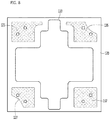
- FIG. 6 is a plan view showing upper portions of a frame and first and second lead frames coupled to a body according to the embodiment
- FIG. 7 is a plan view showing upper portions of the frame and the first and second lead frames according to the embodiment
- FIG. 8 is a plan view showing lower portions of the frame and the first and second lead frames which are coupled to the body according to the embodiment
- FIG. 9 is a plan view showing the lower portions of the frame and the first and second lead frames according to the embodiment.
- a light emitting device package may include the frame 110 exposed through the upper portion of the light emitting device package having the first and second cavities 171 a and 171b provided therein.
- the frame 110 may include first and second stepped parts 113 and 114.
- the first and second stepped parts 113 and 114 may be provided on the frame 110.
- the first and second stepped parts 113 and 114 may have a recess shape and may have a stepped structure when viewed a cross-sectional view, but the embodiment is not limited thereto.
- the first and second stepped parts 113 and 114 may increase the contact area with the body 170 to improve the coupling force with the body 170. Further, the first and second stepped parts 113 and 114 may prevent external moisture from being permeated due to the stepped structure thereof.
- the first and second stepped parts 113 and 114 may be formed by etching portions of a top surface of the frame 110, but embodiment is not limited thereto.
- the thicknesses of the first and second stepped parts 113 and 114 may be 50% of the thickness of the frame 110, but the embodiment is not limited thereto.
- the thicknesses of the first and second stepped parts 113 and 114 may be 50% or more of the thickness of the frame 110.
- the first stepped part 113 may be provided while extending across the central area of the frame 110.
- the first stepped part 113 entirely overlaps the first coupling part 173 of the body 170 and may directly make contact with the first coupling part 173.
- the first stepped part 113 may include first and second grooves 113a and 113b.
- First grooves 113a may be provided at both end portions of the first stepped part 113.
- the first grooves 113a may be symmetrical to each other.
- a portion of the first groove 113a may be provided inside the first cavity 171a and another portion of the first groove part 113a may make contact with the body 170 outside the first cavity 171 a.
- the second grooves 113b may extend from the first grooves 113a.
- the second grooves 113b may be spaced apart from each other by a specific distance.
- the second grooves 113b may be provided in parallel to each other.
- the second grooves 113b may include connection structures to connect the second grooves 113b with each other, but the embodiment is not limited thereto.
- the frame 110 may be divided with two areas inward from the first stepped part 113. In this case, a plurality of light emitting devices may be provided in the two areas.
- the second stepped parts 114 may be spaced apart from the first stepped part 113 by a specific distance.
- the second stepped parts 114 may be symmetrical to each other about the first stepped part 113.
- the second stepped parts 114 may include first and second linear parts 114a and 114b.
- the first linear parts 114a may be provided in parallel with the second grooves 113b of the first stepped part 113.
- the light emitting devices may be interposed between the first linear parts 114a and the first stepped part 113.
- the second linear parts 114b may extend from the central regions of the first linear parts 114a.
- the second linear parts 114b may extend from the first linear parts 114a toward the outer portions of the frame 110.
- the light emitting devices may be provided at both sides of the second linear parts 114b.
- the second linear parts 114b may include end portions 114c making contact with the first cavity 171 a.
- a portion of the end portion 114c may be provided inside the first cavity 171 a and another portion of the end portion 114c may overlap the body 170 outside the first cavity 171 a.
- the end portion 114c may have a fourth width W4 and the second linear part 114b may have a fifth width W5.
- the fourth width W4 of the end portion 114c may be equal to or wider than the fifth width W5 of the second linear part 114b.
- the fourth width W4 of the end portion 114c extending from the body 170 may be equal to or wider than the fifth width W5 of the second linear part 114b, and the injection-molding process for the body 170 may reach even the edge area of the first linear part 114a.
- the reliability of the injection-molding process for the first linear part 114a may be improved due to the end portion 114c having the fourth width W4 equal to or wider than the fifth width W5.
- the fifth width W4 may be 50% to 100% of the fourth width W4.
- the fifth width W5 may be in the range of 0.2 mm to 0.9 mm.
- the fourth width W4 may be in the range of 0.1 mm to 0.9 mm.
- the first linear part 114a may have a width wider than the fifth width W5 of the second linear part 114b, but the embodiment is not limited thereto.
- the first linear part 114a may be 50% to 100% of the fourth width W4, and may be in the range of 0.2 mm to 0.9 mm.
- the frame 110 is provided on the top surface thereof with the first and second stepped parts 113 and 114.
- the first and second stepped parts 113 and 114 are coupled to the first and second coupling parts 173 and 173 of the body 170 to increase the contact area between the body 170 and the frame 110. Accordingly the coupling force between the body 170 and the frame 110 may be improved. In addition, external moisture may be prevented from being permeated due to the stepped structures.
- the third and fourth stepped parts 125 and 127 may be provided on a lower portion of the first lead frame 120.
- the third and fourth stepped parts 125 and 127 may have a recess shape and may have a stepped structure when viewed from a cross-sectional view, but the embodiment is not limited thereto.
- the third and fourth stepped parts 125 and 127 may be supported by a mold frame provided under the first lead frame 120 when the body 170 is subject to an injection-molding process, thereby preventing the first lead frame 120 from being deformed.
- the third and fourth stepped parts 125 and 127 may prevent the first lead frame 120 from being deformed so that the first, second and fifth connection parts 126, 128 and 124 may be formed.
- Portions of the third and fourth stepped parts 125 and 127 may overlap the first, second and fifth connection parts 126, 128 and 124.
- the third and fourth stepped parts 125 and 127 may expose the first, second and fifth connection parts 126, 128 and 124 from the body 170 within the first and second cavities 171 a and 171b.
- the third stepped part 125 may overlap the first pad 121.
- the third stepped part 125 may expose the first pad 121 from the body 170.
- the third and fourth stepped parts 125 and 127 may prevent external moisture from being permeated by the stepped structure.
- the thicknesses of the third and fourth stepped parts 125 and 127 may be 50% of the thickness of the first lead frame 120, but the embodiment is not limited thereto.
- the thicknesses of the third and fourth stepped parts 125 and 127 may be 50% or more of the thickness of the first lead frame 120.
- the fifth and sixth stepped parts 135 and 137 may be provided under the second lead frame 130.
- the fifth and sixth stepped parts 135 and 137 may have a recess shape and may have a stepped structure, but the embodiment is not limited thereto.
- the fifth and sixth stepped parts 135 and 137 are supported by a mold frame provided under the second lead frame 130 when the body 170 is subject to the injection-molding process, thereby preventing the second lead frame 130 from being deformed.
- the fifth and sixth stepped parts 135 and 137 may prevent the second lead frame 130 from being deformed such that the third, fourth and sixth connection parts 136, 138 and 134 are formed.
- Portions of the fifth and sixth stepped parts 135 and 137 may overlap the third, fourth and sixth connection parts 136, 138 and 134.
- the fifth and sixth stepped parts 135 and 137 may exposes the third, fourth, and sixth connection parts 136, 138, and 134 from the body 170 within the first and second cavities 171a and 171b.
- the sixth stepped part 137 may overlap the second pad 131.
- the sixth stepped part 137 may expose the second pad 131 from the body 170.
- the fifth and sixth stepped parts 135 and 137 may prevent external moisture from being permeated by the stepped structure.
- the thicknesses of the fifth and sixth stepped parts 135 and 137 may be 50% of the thickness of the second lead frame 130, but the embodiment is not limited thereto.
- the thicknesses of the fifth and sixth stepped parts 135 and 137 may be 50% or more of the thickness of the second lead frame 130.
- the third and fourth stepped parts 125 and 127 are provided under the first lead frame 120 and the fifth and sixth stepped parts 125 and 127 are provided under the second lead frame 130.
- the third to sixth stepped parts 125, 127, 135, and 137 are supported by the mold frame when the injection-molding process is performed with respect to the body 170, thereby preventing the first and second lead frames 120 and 130 from being deformed.
- the first to sixth connection parts 126, 128, 136, 138, 124, and 134, and the first and second pads 121 and 131, which overlap the third to sixth stepped parts 125, 127, 135, and 137, are exposed from the body 170, thereby preventing the manufacturing defects of the first to sixth connection parts 126, 128, 136, 138, 124, and 134, and the first and second pads 121 and 131.
- external mixture may be prevented from being permeated by the step structure of the third to sixth stepped parts 125, 127, 135, and 137.
- FIG. 10 is a view showing first and second spacers between the frame, and the first and second lead frames according to the embodiment.
- the frame 110, and the first and second lead frames 120 and 130 are included.
- a first spacer 175 may be interposed between the frame 110 and the first lead frame 120, and a second spacer 176 may be interposed between the frame 110 and the second lead frame 130.
- the first spacer 175 may have a sixth width W6.
- the sixth width W6 of the first spacer 175 may be a distance between the frame 110 and the first lead frame 120.
- the first spacer 175 may extend to the outer portion of the light emitting device package.
- a width of the second spacers 176 may be a distance between the frame 110 and the second lead frame 130.
- the first spacer 175 may be symmetrical to the second spacer 176 and may have the overall uniform width, but the embodiment is not limited thereto.
- the frame 110, and the first and second lead frames 120 and 130 may include flexure structures at edges of the light emitting device package.
- the flexure structures may correspond to the structures of the first and second spacers 175 and 176.
- the coupling force between the body 170 and the first frame 110, the coupling force and between the body 170 and the first and second lead frames 120 and 130 may be improved, and the first and second spacers 175 and 176 may be prevented from being cracked due to external force.
- the frame 110 may include the first protrusion parts 110p exposed through the outer portions of the light emitting device package.
- the frame 110 may include a mounting part 110b on which the light emitting devices are mounted and a first flexure part 110a extending from the mounting part 110b.
- the first flexure part 110a may direct make contact with the first protrusion part 110p.
- the first flexure part 110a may have a width greater than the protrusion part 110p.
- the width of the protrusion part 110p may be 20% to 50% of the width of the first flexure part 110a.
- the width of the protruding part 110p is less than 20% of the width of the first flexure part 110a, the strength between adjacent light emitting device packages may be reduced, and thus defects may be caused in a cutting process or the injection molding process of the body 170.
- the width of the protrusion part 110p exceeds 50% of the width of the first flexure part 110a, as the strength of the frame 110, and the first and second lead frames 120 and 130 in a cut area is increased, the body in the cut area may be cracked.
- the coupling force between the body and the frame 110 and the coupling force between the body and the first and second lead frames 120 and 130 may be improved due to the structure of the first flexure part 110a having a width greater than that of the protrusion part 110p.
- the frame 110 and the first and second lead frames 120 and 130 having stronger strength may be easily curt due to the structure of the protrusion part 110p having a width narrower than that of the first flexure part 110a, thereby preventing a peripheral portion of a cut area from being cracked.
- the first lead frame 120 may include the second protrusion parts 120p exposed through the outer portions.
- the first lead frame 120 may include a second flexure part 120a facing the first flexure part 110a.
- the second flexure part 120a may protrude toward the frame 110.
- the second flexure part 120a has a seventh width W7 formed in a first direction X-X' toward the first flexure part 110a and an eighth width W8 formed in a second direction Y-Y perpendicular to the first direction X-X'.
- the seventh width W7 of the second flexure part 120a may be greater than the sixth width W6 of the first spacer 175, but the embodiment is not limited thereto.
- the seventh width W7 of the second flexure part 120a may be 1.2 times to 10 times greater than the sixth width W6 of the first spacer 175.
- the eighth width W8 of the second flexure part 120a may be equal to or greater than the sixth width W6 of the first spacer 175, but the embodiment is not limited thereto.
- the eighth width W8 of the second flexure part 120a may be 1 time to 10 times greater than the sixth width W6 of the first spacer 175.
- the seventh and eighth widths W7 and W8 are less than the sixth width W6, the coupling force between the body 170 and the frame 110, and the coupling force between the body and the first and second lead frames 120 and 130 may be reduced, and the first and second spacers 175 and 176 may not be prevented from being cracked by an external force.
- the seventh and eighth widths W7 and W8 exceed ten times the sixth width W6, the designing of the light emitting device package may be difficult.
- the sixth width W6 may be in the range of 0.2 mm to 0.5 mm, the seventh width W7 may be in the range of 0.24 mm to 2 mm, and the eighth width W8 may be in the range of 0.2 mm to 2 mm.
- the sixth width W6 may be 0.3 mm, the seventh width W7 may be 0.5 mm, and the eighth width W8 may be 0.58 mm.
- the second lead frame 130 may include the third protrusion parts 130p exposed through the outer portions.
- the second lead frame 130 may include a third flexure part 130a facing the first flexure part 110a.
- the details of the third flexure part 130a may be understood by those skilled in art by making reference to the description of the second flexure part 120a, and thus will be omitted below.
- the coupling force between the body 170 and the first and second lead frames 120 and 130 may be improved, and peripheral portions of the first and second spacers 175 and 176 may be prevented from being cracked.
- FIG. 11 is a view showing a first pad area according to the embodiment
- FIG. 12 is a view showing a second pad region according to the embodiment.
- the light emitting device package 100 may include the first and second pads 121 and 122 provided on first and second edges 170a and 170b symmetrical to each other.
- the top surfaces of the first and second pads 121 and 131 may be exposed from the body 170.
- the first pad 121 may include at least one through hole 179.
- the through hole 179 may be filled with a portion of the body 170.
- the through hole 179 may increase the contact area between the first lead frame 120 and the body 170 to improve the coupling force between the body 170 and the first lead frame 120.
- the first protective part 177 covering the outer portion of the first pad 121 and a second protective part 178 covering the outer portion of the second pad 131 may be included.
- the first and second protective parts 177 and 178 may be included in the body 170.
- the first protective part 177 is provided at an outer portion of the first pad 121 to directly make contact with the first pad 121
- the second protective part 178 is provided at an outer portion of the second pad 131 to directly make contact with the second pad 131.
- the first and second protective parts 177 and 178 are provided outside the first and second corners 170a and 170b to protect the first and second pads 121 and 131 from the outside.
- the first protective part 177 may be interposed between the second protrusion parts 120p extending from the first pad 121.
- the first protective part 177 may include third and fourth linear parts 177a and 177b.
- the third and fourth linear parts 177a and 177b may directly make contact with the second protrusion parts 120p.
- the third and fourth linear parts 177a and 177b may be connected with each other.
- the third and fourth linear parts 177a and 177b may directly make contact with the outer portion of the first pad 121 exposed between the second protrusion parts 120p.
- the second protective part 178 may be interposed between the third protrusion parts 130p extending from the second pad 131.
- the second protective part 178 may include fifth and sixth linear parts 178a and 178b.
- the fifth and sixth linear parts 178a and 178b may directly make contact with the third protrusion parts 130p.
- the fifth and sixth linear parts 178a and 178b may be connected to each other.
- the fifth and sixth linear parts 178a and 178b may directly make contact with the outer portions of the second pad 131 exposed between the third projections 130p.
- the first and second protective parts 177 and 178 which cover the outer portions of the first and second pads 121 and 131, are included to protect the first and second pads 121 and 131 and to improve the coupling force between the body 170 and the first and second lead frames 120 and 130.
- at least one through hole 179 is formed through the first and second pads 121 and 131 to improve the coupling force between the body 170 and the first and second lead frames 120 and 130.
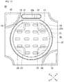
- FIG. 13 is a perspective view showing a light emitting device package according to another embodiment.
- a light emitting device package 200 may include a reflective part 290.
- the light emitting device package 200 may employ the technical features of the light emitting device package 100 in the previous embodiment of FIGS. 1 to 12 except for the reflective part 290.
- the body 170 may include the reflective part 290 inside the first cavity 171a.
- the reflective part 290 may include sub-cavities 290a individually surrounding the relevant light emitting devices 150.
- the reflective part 290 may be defined as a part protruding upward from the bottom of the first cavity 171 a.
- the reflective part 290 may correspond to the arrangement structure of the light emitting devices 150.
- the reflective part 290 may be formed in a matrix type, but the embodiment is not limited thereto.
- the reflective part 290 may include the sub-cavities 290a corresponding to the light-emitting devices 150 in number.
- the reflective part 290 may include 16 sub-cavities 290a corresponding to 16 light emitting devices 150, but the embodiment is not limited thereto.
- the reflective part 290 may have a width which gradually decreases upward.
- the reflective part 290 may include inclined side surfaces, but is not limited thereto.
- the reflective part 290 may include sides of a curved structure.
- the widths of upper and lower portions of the reflective part 290 may employ the technical features of the first and second reflective partitions 191 and 193 in the previous embodiment.
- the reflective part 290 may have a height lower than that of the inner surface of the first cavity 171a, but the embodiment is not limited thereto.
- the height of the reflective part 290 may be equal to or higher than that of the light emitting device 150.
- the height of the reflective part 290 may be equal to or lower than the inner surface of the first cavity 171 a.
- the matrix-type reflective part 290 may be included in the COB light emitting device package 200 to reflect light, which is emitted from the light emitting devices 150, to the outside, thereby improving the light extraction efficiency.
- the deformation of the light emitting device package 200 resulting from the contraction and the expansion of the light emitting device package 200 may be prevented by the matrix-type reflective part 190 provided in the first cavity 171a in which the light emitting devices 150 are mounted.
- the deformation of a molding part (not shown) resulting from the contraction and the expansion of the molding part provided in the first cavity 171a may be prevented by the matrix-type reflective part 190 provided in the first cavity 171a in which the light emitting devices 150 are mounted.
- the deformation of the molding part may be prevented, thereby preventing the damage to the wire 150W caused by the deformation of the molding part.
- the light extraction efficiency of the light emitting device package 200 may be improved by refracting light from the light emitting device 150 in various directions.
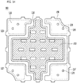
- FIGS. 14 and 15 are plan views showing a light emitting device package according to still another embodiment.
- a light emitting device package 300 may include a stepped part 313 and a coupling part 373. According to still another embodiment, the light emitting device package 300 may employ the technical features of the light emitting device package 100 shown in FIGS. 1 to 12 in the previous embodiment except for the stepped part 313 and the coupling part 373.
- the frame 110 may include the stepped part 313.
- the stepped part 313 may be provided on the frame 110.
- the stepped part 313 may have a recess shape, and may have a stepped structure when viewed a cross-sectional view, but the embodiment is not limited thereto.
- the stepped part 313 may increase the contact area with the body 170 to improve the coupling force with the body 170. Further, the stepped part 313 may prevent external moisture from being permeated due to the stepped structure.
- the stepped part 313 may be formed by etching a portion of the top surface of the frame 110, but the embodiment is not limited thereto.
- the thickness of the stepped part 313 may be 50% of the thickness of the frame 110, but the embodiment is not limited thereto.
- the thickness of the stepped part 313 may be 50% or more of the thickness of the frame 110.
- the stepped parts 313 may be spaced apart from the frame 110 by a specific distance along the edge of the frame 110.
- the frame 110 may be provided on the bottom surface thereof with a lower stepped structure (not shown) formed along the edge of the frame 110.
- the stepped part 313 may be spaced apart from the frame 110 by the specific distance along the edge of the frame 110 such that the stepped part 313 does not overlap the lower stepped structure, but the embodiment is not limited thereto.
- the stepped part 313 may be provided up to the edge of the top surface of the frame 110.
- the frame 110 may include a plurality of light emitting device mounting parts 350 formed on the top surface.
- the thicknesses of the light emitting device mounting parts 350 may correspond to the thickness of the frame 110.
- the contact area between the coupling part 373 and the frame 110 is increased to improve the coupling force between the body 170 and the frame 110.
- the stepped part 313 may entirely overlap the coupling part 373 of the body 170 and may make contact with the coupling part 373.
- the top surface of the coupling part 373 may be aligned in line with top surfaces of the light emitting device mounting parts 350.
- the stepped part 313 is provided in an area except for the light emitting device mounting parts 350, and are coupled to the coupling part 373 of the body 170 to increase the contact area between the body 170 and the frame 110, the coupling force between the body 170 and the frame 110 may be improved, and external moisture may be prevented from being permeated due to the stepped structures.
- the light emitting device package may be applied to a display device, a lighting unit, an indicator, a lamp, a street lamp, a lighting device for a vehicle, a display device for the vehicle, a smart watch, and the like, but the embodiment is not limited thereto.
- the light emitting device package When the light emitting device package is used for a backlight unit of a display device, the light emitting device package may be used for an edge-type backlight unit or a direct-type backlight unit. When the light emitting device package is used for a light source of a lighting device, the light emitting device package may be used in a lighting device type or a bulb type, or may be used for a light source of a mobile terminal.
- a semiconductor device includes a laser diode in addition to a light emitting diode.
- the semiconductor device may not be implemented only with a semiconductor. If necessary, the semiconductor device may further include a metallic material.
- a semiconductor device serving as a light receiving device may be implemented with at least Ag, Al, Au, In, Ga, N, Zn, Se, P, or As, or may be implemented with a semiconductor material doped with P-type dopants or N-type dopants, or an intrinsic semiconductor material.
Landscapes
- Led Device Packages (AREA)
- Non-Portable Lighting Devices Or Systems Thereof (AREA)
Abstract
Description
- The embodiment relates to a light emitting device package and a lighting device having the same.
- A light emitting diode includes a P-N junction diode having a characteristic of converting electrical energy into light energy. The light emitting device may be fabricated with compound semiconductors belonging to group III and V on the periodic table. The light-emitting device can produce various colors by adjusting the compositional ratio of the compound semiconductors.
- When forward voltage is applied to the light emitting device, electrons of an N layer are combined with holes of a P layer, so that energy corresponding to an energy gap between a conduction band and a valance band may be generated. The energy is mainly generated in the form of heat or light. In the case of the light emitting device, the energy is generated in the form of light.
- For example, a nitride semiconductor represents superior thermal stability and wide bandgap energy so that the nitride semiconductor has been spotlighted in the field of optical devices and high-power electronic devices. Specifically, blue light emitting devices, green light emitting devices, ultraviolet (UV) light emitting devices, and the like using nitride semiconductors are commercialized and widely used.
- Recently, as the brightness of a light emitting diode has been significantly improved, the light emitting diode has been applied to various devices such as a backlight unit of a liquid crystal display, an electric signboard, an indicator, and a home appliance.
- The embodiment provides a light emitting device package, capable of improving light extraction efficiency, and a lighting device having the same.
- The embodiment provides a light emitting device package, capable of improving coupling force between components, and a lighting device having the same.
- The embodiment provides a chip-on-board (COB) light emitting device package having a stabile structure and a lighting device having the same.
- According to the embodiment, the light emitting device package includes a frame, a first lead frame spaced apart from the frame by a specific distance, a second lead frame spaced apart from the frame by the specific distance, a body coupled to the frame and the first and second lead frames and having a first cavity, and a plurality of light emitting devices provided on the frame exposed through the first cavity, in which the body includes a reflective part which is provided inside the first cavity to surround at least one of the light emitting devices, thereby improving light extraction efficiency. According to the embodiment, the deformation of the light emitting device package resulting from the contraction and the expansion of the light emitting device package can be prevented by the reflective part. According to the embodiment, the deformation of a molding part resulting from the contraction and the expansion of the molding part provided in the first cavity can be prevented by the reflective part. In other words, according to the embodiment, the deformation of the molding part can be prevented, thereby preventing the damage to a wire resulting from the deformation of the molding part.
- According to the embodiment, a lighting device may include the light emitting device package.
- As described above, according to the light emitting device package of the embodiment, the deformation of the light emitting device package resulting from the contraction and the expansion of the light emitting device package can be prevented by the reflective part extending across the central area of the cavity in which the light emitting devices are mounted.
- According to the embodiment, the deformation of the molding part resulting from the contraction and the expansion of the molding part provided in the first cavity can be prevented by the reflective part extending across the central area of the cavity in which the light emitting devices are mounted. In other words, according to the embodiment, the deformation of the molding part can be prevented, thereby preventing the damage to the wire resulting from the deformation of the molding part.
- According to the embodiment, as the stepped part is provided on the top surface of the heat sinking plate, the coupling force between the heat sinking plate and the body can be improved, and the external moisture can be prevented from being permeated due to the stepped structure.
- According to the embodiment, the stepped parts are provided on the lower portions of the first and second lead frames and supported by a mold frame to prevent the first and second lead frames from being deformed. In addition, the reliability of the injection-molding process of the body that exposes the connection parts and the pads from the body through the cavity. Further, the external moisture can be prevented from being permeated due to the stepped structures formed on the lower portion of the first and second lead frames.
- According to the embodiment, flexure structures are provided at edges of the first and second lead frames only to improve the coupling force with the body, but also to prevent a peripheral portion of the spacer, which is provided between the first and second frames, from being cracked.
- According to the embodiment, the protective part, which covers the outer portion of the pad, is included to protect the pad and to improve the coupling force between the body and the first and second lead frames. In addition, according to the embodiment, at least one through hole is formed through the pad to improve the coupling force between the body and the first and second lead frames.
- The present disclosure will become more fully understood from the detailed description given herein below and the accompanying drawings, which are given by illustration only, and thus are not limitative of the present disclosure, and wherein:
-
FIG. 1 is a perspective view showing a light emitting device package according to the embodiment; -
FIG. 2 is a sectional view showing a light emitting device package according to the embodiment; -
FIG. 3 is a plan view showing a light emitting device package according to the embodiment; -
FIG. 4 is a plan view showing a reflective part according to the embodiment; -
FIG. 5 is a plan view showing a reflective part and a first coupling part according to the embodiment; -
FIG. 6 is a plan view showing upper portions of a frame and first and second lead frames coupled to a body according to the embodiment; -
FIG. 7 is a plan view showing upper portions of a frame and first and second lead frames according to the embodiment; -
FIG. 8 is a plan view showing lower portions of a frame and first and second lead frames which are coupled to the body according to the embodiment; -
FIG. 9 is a plan view showing lower portions of a frame and first and second lead frames according to the embodiment; -
FIG. 10 is a view showing first and second spacers between the frame, and first and second lead frames according to the embodiment; -
FIG. 11 is a view showing a first pad area according to the embodiment; -
FIG. 12 is a view showing a second pad region according to the embodiment. -
FIG. 13 is a perspective view showing a light emitting device package according to another embodiment; and -
FIGS. 14 and15 plan views showing a light emitting device package according to still another embodiment. - Variations, modifications, and the combination of the embodiments are possible, and the present disclosure is not limited to the embodiments to be described below.
- Although the matters described in the specific embodiments are not described in the other embodiments, other embodiments may be understood as being related to the other embodiments unless otherwise specified or contradicted by those in the other embodiments.
- For example, if the features for configuration A are described in a specific embodiment, and the features for configuration B are described in another embodiment, even if embodiments in which configuration A and configuration B are combined are not explicitly described, it should be understood that they fall within the scope of the present disclosure unless otherwise specified or contradicted.
- Hereinafter, the embodiments of the present disclosure will be described in detail in order to accomplish the above objects of the present disclosure.
- In the following description of the embodiments, it will be understood that, when each of elements are referred to as being "on" or "under" another element, it can be "directly" or "indirectly" on the element, or one or more intervening element may also be present. In addition, if the element is expressed in association with the terms "on" or "under", the direction of the element include the lower direction of the element as well as the upper direction of the element.
- A semiconductor device may include various electronic devices such as a light emitting device, a light receiving device, and the like. The light emitting device and the light receiving device may include a first conductive type semiconductor layer, an active layer, and a second conductive type semiconductor layer.
- According to the embodiment, the semiconductor device may be the light emitting device.
- The light emitting device emits light through the recombination between electrons and holes, and the wavelength of the light is determined depending on the intrinsic energy band gap of the material. Accordingly, the emitted light may be varied with the composition of the material.
-
FIG. 1 is a perspective view showing a light emitting device package according to the embodiment.FIG. 2 is a sectional view showing the light emitting device package according to the embodiment.FIG. 3 is a plan view showing the light emitting device package according to the embodiment.FIG. 4 is a plan view showing a reflective part according to the embodiment.FIG. 5 is a plan view showing the reflective part and a first coupling part according to the embodiment. - As shown in
FIGS. 1 to 5 , according to the embodiment, the lightemitting device package 100 may include a frame (heat sinking plate) 110, afirst lead frame 120, asecond lead frame 130, abody 170, aprotective device 160, and a plurality oflight emitting devices 150. According to the embodiment, in the lightemitting device package 100, theprotective device 160 and thelight emitting devices 150 may be mounted on theframe 110. The first and second lead frames 120 and 130 may be spaced apart from theframe 110 by a specific distance. According to the embodiment, the light emittingdevice package 100 may be a chip-on-board (COB) light emitting device package. For example, according to the embodiment, the light emittingdevice package 100 may be directly die-bonded onto a substrate and electrically connected with the substrate through a wire, but the embodiment is not limited thereto. - The
body 170 may include at least one of a transmissive material, a reflective material, and an insulating material. Thebody 170 may include a material having a reflectance higher than transmittance with respect to light emitted from thelight emitting devices 150. Thebody 170 may include a resin-based insulating material. For example, thebody 170 may include at least one of a resin material, such as polyphthalamide (PPA), epoxy, or a silicone material, silicon (Si), a metallic material, photo sensitive glass (PSG), sapphire (Al2O3), and a printed circuit board (PCB). Thebody 170 may include four corners. - The
body 170 may include first andsecond corners fourth corners first pad 121 of thefirst lead frame 120 may be exposed through thefirst corner 170a. Asecond pad 131 of thesecond lead frame 130 may be exposed through thesecond corner 170b. The first andsecond corners second pads second corners second pads second corners second pads fourth corners device package 100. The third andfourth corners fourth corners fourth corners - The
body 170 may be coupled to theframe 110, and the first and second lead frames 120 and 130. Thebody 170 may include afirst cavity 171 a and asecond cavity 171 b which expose portions of top surfaces of theframe 110 and the first and second lead frames 120 and 130. Thefirst cavity 171 a may extend from the central area of thebody 170. Thefirst cavity 171 a may be provided in an area on which thelight emitting devices 150 are mounted. Thefirst cavity 171a may have a circular shape when viewed from a top view, but the embodiment is not limited thereto. For example, thefirst cavity 171a may have an oval shape or at least three polygonal shapes when viewed from the top view. Thesecond cavity 171b may be spaced from thefirst cavity 171a by a specific distance. Thesecond cavity 171b may be adjacent to one lateral side of thebody 170, and may be interposed between one lateral side of thebody 170 and thefirst cavity 171a. Thesecond cavity 171b may be spaced apart from the lateral side of thebody 170 by a specific distance. The distance between thesecond cavity 171b and thefirst cavity 171a may be 0.1 mm or more. The distance between thesecond cavity 171b and the lateral side of thebody 170 may be 0.1 mm or more. According to the embodiment, as the distance between the lateral side of thebody 170 and thesecond cavity 171b is 0.1 mm or more, and the distance between the first andsecond cavities second cavities body 170 and thesecond cavity 171b or the distance between the first cavity 171 and thesecond cavity 171b is less than 0.1 mm, defects may be caused in an injection molding process of the first andsecond cavities second cavity 171b may be interposed between the first andthird corners second cavity 171b may be provided in an area on which theprotective device 160 is mounted. Thesecond cavity 171b may have a diameter less than that of thefirst cavity 171a. For example, thesecond cavity 171b may have a bottom surface area narrower than that of thefirst cavity 171a. The area of thesecond cavity 171b may be 10-25% of the area of thefirst cavity 171a. Anarrower width 171W of thesecond cavity 171b may be 2%-6% of the entire width of the light emittingdevice package 100. When thenarrower width 171W of thesecond cavity 171b is less than 2% of the entire width of the light emittingdevice package 100, the size of theprotective device 160 is limited, so that the stability of the light emittingdevice package 100 may be degraded. When thenarrower width 171W of thesecond cavity 171b exceeds 6% of the entire width of the light emittingdevice package 100, as the size of the light emittingdevice package 100 may be increased except for a light emitting area in which light is emitted, the application of the light emittingdevice package 100 to various fields may be limited. For example, thenarrower width 171W of thesecond cavity 171b may be in the range of 0.150 mm to 0.450 mm. - The
body 170 may include four outer portions, each of which is provided between two adjacent corners among the first tofourth corners 171a to 17d. The four outer portions may be flat planes. According to the embodiment, a portion of theframe 110 and portions of the first and second lead frames 120 and 130 may be exposed through the outer portions. For example,first protrusion parts 110p may extend from theframe 110 through an outer portion of thebody 170. In this case, thefirst protrusion parts 110p may be formed in a unit package cutting process after the injection-molding process of thebody 170 is performed. In other words, thefirst protrusion parts 110p may be engagement parts which engage adjacent frames with each other before the unit package cutting process is performed.Second protrusion parts 120p may be provided at the outer portions of thebody 170 while extending from thefirst lead frame 120. In this case, thesecond protrusion parts 120p may be formed in a unit package cutting process after the injection-molding process of thebody 170 is performed. In other words, thesecond protrusion parts 120p may be engagement parts which engage adjacent first lead frames frames to each other before the unit package cutting process is performed.Third protrusion parts 130p may be provided at the outer portions of thebody 170 while extending from thesecond lead frame 130. In this case, thethird protrusion parts 130p may be formed in a unit package cutting process after the injection-molding process of thebody 170 is performed. In other words, thethird protrusion parts 130p may be connection parts which connect adjacent second lead frames frames with each other before the unit package cutting process is performed. - The
body 170 may include first andsecond spacers first spacer 175 may be interposed between theframe 110 and thefirst lead frame 120. Thesecond spacer 176 may be interposed between theframe 110 and thesecond lead frame 130. - The
body 170 may include first andsecond coupling parts second coupling parts frame 110. The first andsecond coupling parts body 170 and theframe 110. The first andsecond coupling parts body 170 and theframe 110. The first andsecond coupling parts frame 110 on which thelight emitting devices 150 are mounted. The first andsecond coupling parts frame 110. The stepped part may be a groove structure provided in the top surface of theframe 110 and having a concave shape. The stepped part will be described in detail with reference toFIGS. 8 and9 later. The first andsecond coupling parts frame 110. - The
body 170 may include areflective part 190 inside thefirst cavity 171a. Thereflective part 190 may include first to thirdreflective partitions reflective partitions first coupling part 173 provided on the top surface of theframe 110. For example, the first to thirdreflective partitions first coupling part 173. The first to thirdreflective partitions first coupling part 173. The first to thirdreflective partitions first cavity 171a. The first and secondreflective partitions first cavity 171a. The first and secondreflective partitions first cavity 171 a. The first and secondreflective partitions reflective partitions reflective partition 195 may be interposed between the first and secondreflective partitions reflective partition 195 may be provided at intermediate points of the first and secondreflective partitions reflective part 190 may be divided into two areas by the first to thirdreflective partitions - The first to third
reflective partitions reflective partitions reflective partitions reflective partitions first coupling part 173. The first and secondreflective partitions first coupling part 173. The upper portions of the first and secondreflective partitions reflective partitions reflective partitions first coupling part 173. The first width W1 of the first and secondreflective partitions reflective partitions light emitting devices 150 while being perpendicular to the lateral sides of thelight emitting devices 150. - The lower portions of the first and second
reflective partitions first coupling part 173 and thereflective part 190. The second width W2 of the first and secondreflective partitions reflective partition 195. The third width W3 of the thirdreflective partition 195 may be equal to or greater than the second width W2 of the first and secondreflective partitions reflective partition 195 may be 2 to 10 times greater than the second width W2 of the first and secondreflective partitions reflective partition 195 may be in the range of 0.4 mm to 2.0 mm. - When the third width W3 of the third
reflective partition 195 is less than 0.4 mm, since the distance between adjacent light emittingdevices 150 is increased, a reflective function may be degraded. When the third width W3 of the thirdreflective partition 195 exceeds 2. 0 mm, a dark part may be formed by the thirdreflective partition 195, and the inner space defined by the first to thirdreflective partitions light emitting devices 150 are arranged in the inner space. - The widths of the lower portions of the first to third
reflective partitions first coupling part 173. In this case, thefirst coupling part 173 may include first andsecond extension parts first extension parts 173a may directly make contact with the inner surface of thefirst cavity 171a in thebody 170. Thefirst extension parts 173a may face each other on the inner surface of thefirst cavity 171a in thebody 170.Second extension parts 173b may be interposed between thefirst extension parts 173a. Thesecond extension parts 173b may be spaced apart from each other by a specific distance. Thesecond extension parts 173b may be provided under the first and secondreflective partitions second extension part 173b may be provided under the thirdreflective partition 195 and may have a width wider than that of the thirdreflective partition 195, but the embodiment is not limited thereto. The first andsecond extension parts reflective part 190. - A distance 173W1 between the
first extension parts 173a may be 2 to 12 times greater than the second width W2. The width of eachsecond extension part 173b may be 1.0 to 5 times greater than the second width W2. The width of thefirst extension part 173a may be in the range of 1.5 mm to 2.5 mm, and the width of eachsecond extension part 173b may be in the range of 0.2 mm to 0. 9 mm. The distance 173W1 between thefirst extension parts 173a may be greater than adistance 191W between the first and secondreflective partitions second extension parts 173b may be less than thedistance 191W between the first and secondreflective partitions second extension parts reflective part 190, the reliability of an injection-molding process may be improved when thereflective part 190 is fabricated. - The first to third
reflective partitions first cavity 171a, but the embodiment is not limited thereto. The height H1 of the first to thirdreflective partitions light emitting devices 150. The height H1 of the first to thirdreflective partitions first cavity 171a. - The
reflective part 190 may include first and secondcurved parts reflective partitions reflective partition 195. The first andsecond curve parts reflective partitions reflective partition 195 and thus refract light, which is emitted from thelight emitting devices 150, in various directions, thereby improving light extraction efficiency of the light emittingdevice package 100. - The
light emitting devices 150 may be provided on theframe 110. Thelight emitting devices 150 may be provided on theframe 110 exposed from thebody 170. According to the embodiment, thelight emitting devices 150 are parallel-connected with each other in the form of two groups. In this case, thelight emitting devices 150 may be electrically connected with each other through awire 150w. Although the embodiment is limited to the configuration that thelight emitting devices 150 are parallel-connected with each other in the form of two groups as described above, the embodiment is not limited thereto. For example, thelight emitting devices 150 may be parallel-connected with each other in the form of multiple groups. Thelight emitting devices 150 may be electrically connected with the first and second lead frames 120 and 130. Thelight emitting devices 150 may be electrically connected with the first and second lead frames 120 and 130 through thewire 150w. A first group of light emittingdevices 150 may be series-connected with each other through thewire 150w and thus may be connected with first tofourth connection parts first cavity 171a. In this case, the first andsecond connection parts first lead frame 120. Top surfaces of the first andsecond connection parts body 170 within thefirst cavity 171a. The third and fourth connectingparts second lead frame 130. Top surfaces of the third andfourth connection parts body 170 within thefirst cavity 171a. - In this case, according to the embodiment, the first and second lead frames 120 and 130 are included. The
first lead frame 120 may include third and fourth steppedparts second lead frame 130 may include fifth and sixth steppedparts - The
first connection part 126 may extend from the third steppedpart 125. Thesecond connection part 128 may extend from the fourth steppedpart 127. - The area of the
first connection part 126 may be 3% to 10% of that of the third steppedpart 125. The area of thesecond connection part 128 may be 3% to 10% of that of of thefourth step 127. When the area of thefirst connection part 126 is less than 3% of that of the third steppedpart 125, the minimum area for bonding of thewire 150w is not ensured, and thus the bonding reliability may be degraded. When the area of thesecond connection part 128 is less than 3% of the area of the fourth steppedpart 127, the minimum area for bonding of thewire 150w is not secured, and thus the bonding reliability may be degraded. When the area of thefirst connection part 126 exceeds 10% of the area of the third steppedpart 125, the arrangement areas of thelight emitting devices 150 may be reduced, and thus the degree of freedom may be reduced in the arrangement of thelight emitting devices 150. When the area of thesecond connection part 128 exceeds 10% of the area of the fourth steppedpart 127, the arrangement areas of thelight emitting devices 150 may be reduced, and thus the degree of freedom may be reduced in the arrangement of thelight emitting devices 150. - The
third connection part 136 may extend from the fifth steppedpart 135. Thefourth connection part 138 may extend from thesixth step 137. - The area of the
third connection part 136 may be 3% to 10% of the area of the fifth steppedpart 135. The area of thefourth connection part 138 may be 3% to 10% of the area of the sixth steppedpart 137. When the area of thethird connection part 136 is less than 3% of the area of the fifth steppedpart 135, the minimum area for bonding of thewire 150w may not be ensured, and thus the bonding reliability may be degraded. When the area of thefourth connection part 138 is less than 3% of the area of the sixth steppedpart 137, the minimum area for bonding of thewire 150w may not be ensured, and thus bonding reliability may be degraded. When the area of thethird connection part 136 exceeds 10% of the area of the fifth steppedpart 135, the arrangement areas of thelight emitting devices 150 are reduced, and thus the degree of freedom may be reduced in the arrangement of thelight emitting devices 150. When the area of thefourth connection part 138 exceeds 10% of the area of thesixth step part 137, the arrangement areas of thelight emitting devices 150 may be reduced, and thus the degree of freedom may be reduced in the arrangement of thelight emitting devices 150. - The width between the
first connection part 126 and the inner surface of thefirst cavity 171 a may be in the range of 30 µm to 100 µm. The width between the second connectingpart 128 and the inner surface of thefirst cavity 171 a may be in the range of 30 µm to 100 µm. The width between thethird connection part 136 and the inner surface of thefirst cavity 171 a may be in the range of 30 µm to 100 µm. The width between thefourth connection part 138 and the inner surface of thefirst cavity 171a may be in the range of 30 µm to 100 µm. When the width between each of the first tofourth connection parts first cavity 171a is less than 30 µm, the minimum area for the bonding of thewire 150w may not be ensured, and thus the bonding reliability can be degraded. When the width between each of the first tofourth connection parts first cavity 171a exceeds 100 µm, the arrangement areas of thelight emitting devices 150 may be reduced, and thus the degree of freedom may be reduced in the arrangement of thelight emitting devices 150. - According to the embodiment, the areas and the widths of the first to
fourth connection parts light emitting devices 150. - The
protective device 160 may be provided on theframe 110. Theprotection element 160 may be provided on the top surface of theframe 110 exposed through the bottom of thesecond cavity 171 b. Theprotective device 160 may be a zener diode, a thyristor, a transient voltage suppression (TVS), or the like, but the embodiment is not limited thereto. According to the embodiment, theprotective device 160 may be a zener diode which protects thelight emitting devices 150 from electrostatic discharge (ESD) for the illustrative purpose in the following description. Theprotective device 160 may be connected with the first and second lead frames 120 and 130 through wires. Theprotective device 160 may be connected with fifth andsixth connection parts second cavity 171b. In this case, thefifth connection part 124 may be a portion of thefirst lead frame 120. A top surface of thefifth connection part 124 may be exposed from thebody 170 within thesecond cavity 171b. Thesixth connection part 134 may be a portion of thesecond lead frame 130. The top surface of thesixth connection part 134 may be exposed from thebody 170 within thesecond cavity 171 b. - As shown in
FIGS. 1 to 5 , according to the embodiment, thereflective part 190 may be included in the COB light emittingdevice package 100 to reflect light, which is emitted from thelight emitting devices 150, to the outside, thereby improving the light extraction efficiency. - According to the embodiment, the deformation of the light emitting
device package 100 resulting from the contraction and the expansion of the light emittingdevice package 100 may be prevented by thereflective part 190 provided in thefirst cavity 171a in which thelight emitting devices 150 are mounted. - According to the embodiment, the deformation of a molding part (not shown) resulting from the contraction and the expansion of the molding part provided in the
first cavity 171 a may be prevented by thereflective part 190 provided in thefirst cavity 171 a in which thelight emitting devices 150 are mounted. In other words, according to the embodiment, the deformation of the molding part is prevented, and thus thewire 150w may be prevented from being damaged due to the deformation of the molding part. -
FIG. 6 is a plan view showing upper portions of a frame and first and second lead frames coupled to a body according to the embodiment, andFIG. 7 is a plan view showing upper portions of the frame and the first and second lead frames according to the embodiment.FIG. 8 is a plan view showing lower portions of the frame and the first and second lead frames which are coupled to the body according to the embodiment, andFIG. 9 is a plan view showing the lower portions of the frame and the first and second lead frames according to the embodiment. - As shown in
FIGS. 6 to 9 , according to the embodiment, a light emitting device package may include theframe 110 exposed through the upper portion of the light emitting device package having the first andsecond cavities frame 110 may include first and second steppedparts - The first and second stepped
parts frame 110. The first and second steppedparts parts body 170 to improve the coupling force with thebody 170. Further, the first and second steppedparts parts frame 110, but embodiment is not limited thereto. The thicknesses of the first and second steppedparts frame 110, but the embodiment is not limited thereto. For example, the thicknesses of the first and second steppedparts frame 110. The first steppedpart 113 may be provided while extending across the central area of theframe 110. The first steppedpart 113 entirely overlaps thefirst coupling part 173 of thebody 170 and may directly make contact with thefirst coupling part 173. The first steppedpart 113 may include first andsecond grooves First grooves 113a may be provided at both end portions of the first steppedpart 113. Thefirst grooves 113a may be symmetrical to each other. A portion of thefirst groove 113a may be provided inside thefirst cavity 171a and another portion of thefirst groove part 113a may make contact with thebody 170 outside thefirst cavity 171 a. Thesecond grooves 113b may extend from thefirst grooves 113a. Thesecond grooves 113b may be spaced apart from each other by a specific distance. Thesecond grooves 113b may be provided in parallel to each other. Thesecond grooves 113b may include connection structures to connect thesecond grooves 113b with each other, but the embodiment is not limited thereto. Theframe 110 may be divided with two areas inward from the first steppedpart 113. In this case, a plurality of light emitting devices may be provided in the two areas. - The second stepped
parts 114 may be spaced apart from the first steppedpart 113 by a specific distance. The second steppedparts 114 may be symmetrical to each other about the first steppedpart 113. The second steppedparts 114 may include first and secondlinear parts linear parts 114a may be provided in parallel with thesecond grooves 113b of the first steppedpart 113. In this case, the light emitting devices may be interposed between the firstlinear parts 114a and the first steppedpart 113. The secondlinear parts 114b may extend from the central regions of the firstlinear parts 114a. The secondlinear parts 114b may extend from the firstlinear parts 114a toward the outer portions of theframe 110. In this case, the light emitting devices may be provided at both sides of the secondlinear parts 114b. The secondlinear parts 114b may include endportions 114c making contact with thefirst cavity 171 a. A portion of theend portion 114c may be provided inside thefirst cavity 171 a and another portion of theend portion 114c may overlap thebody 170 outside thefirst cavity 171 a. - The
end portion 114c may have a fourth width W4 and the secondlinear part 114b may have a fifth width W5. The fourth width W4 of theend portion 114c may be equal to or wider than the fifth width W5 of the secondlinear part 114b. According to the embodiment, the fourth width W4 of theend portion 114c extending from thebody 170 may be equal to or wider than the fifth width W5 of the secondlinear part 114b, and the injection-molding process for thebody 170 may reach even the edge area of the firstlinear part 114a. That is to say, according to the embodiment, the reliability of the injection-molding process for the firstlinear part 114a, which is provided farthest from thefirst cavity 171a, may be improved due to theend portion 114c having the fourth width W4 equal to or wider than the fifth width W5. According to the embodiment, the fifth width W4 may be 50% to 100% of the fourth width W4. The fifth width W5 may be in the range of 0.2 mm to 0.9 mm. The fourth width W4 may be in the range of 0.1 mm to 0.9 mm. In this case, the firstlinear part 114a may have a width wider than the fifth width W5 of the secondlinear part 114b, but the embodiment is not limited thereto. For example, the firstlinear part 114a may be 50% to 100% of the fourth width W4, and may be in the range of 0.2 mm to 0.9 mm. - According to the embodiment, the
frame 110 is provided on the top surface thereof with the first and second steppedparts parts second coupling parts body 170 to increase the contact area between thebody 170 and theframe 110. Accordingly the coupling force between thebody 170 and theframe 110 may be improved. In addition, external moisture may be prevented from being permeated due to the stepped structures. - The third and fourth stepped
parts first lead frame 120. The third and fourth steppedparts parts first lead frame 120 when thebody 170 is subject to an injection-molding process, thereby preventing thefirst lead frame 120 from being deformed. In addition, the third and fourth steppedparts first lead frame 120 from being deformed so that the first, second andfifth connection parts parts fifth connection parts parts fifth connection parts body 170 within the first andsecond cavities part 125 may overlap thefirst pad 121. The third steppedpart 125 may expose thefirst pad 121 from thebody 170. The third and fourth steppedparts parts first lead frame 120, but the embodiment is not limited thereto. For example, the thicknesses of the third and fourth steppedparts first lead frame 120. - The fifth and sixth stepped
parts second lead frame 130. The fifth and sixth steppedparts parts second lead frame 130 when thebody 170 is subject to the injection-molding process, thereby preventing thesecond lead frame 130 from being deformed. The fifth and sixth steppedparts second lead frame 130 from being deformed such that the third, fourth andsixth connection parts parts sixth connection parts parts sixth connection parts body 170 within the first andsecond cavities part 137 may overlap thesecond pad 131. The sixth steppedpart 137 may expose thesecond pad 131 from thebody 170. The fifth and sixth steppedparts parts second lead frame 130, but the embodiment is not limited thereto. For example, the thicknesses of the fifth and sixth steppedparts second lead frame 130. - According to the embodiment, the third and fourth stepped
parts first lead frame 120 and the fifth and sixth steppedparts second lead frame 130. The third to sixth steppedparts body 170, thereby preventing the first and second lead frames 120 and 130 from being deformed. According to the embodiment, the first tosixth connection parts second pads parts body 170, thereby preventing the manufacturing defects of the first tosixth connection parts second pads parts -
FIG. 10 is a view showing first and second spacers between the frame, and the first and second lead frames according to the embodiment. - As shown in
FIG. 10 , according the embodiment, theframe 110, and the first and second lead frames 120 and 130 are included. Afirst spacer 175 may be interposed between theframe 110 and thefirst lead frame 120, and asecond spacer 176 may be interposed between theframe 110 and thesecond lead frame 130. - The
first spacer 175 may have a sixth width W6. The sixth width W6 of thefirst spacer 175 may be a distance between theframe 110 and thefirst lead frame 120. Thefirst spacer 175 may extend to the outer portion of the light emitting device package. A width of thesecond spacers 176 may be a distance between theframe 110 and thesecond lead frame 130. Thefirst spacer 175 may be symmetrical to thesecond spacer 176 and may have the overall uniform width, but the embodiment is not limited thereto. - The
frame 110, and the first and second lead frames 120 and 130 may include flexure structures at edges of the light emitting device package. The flexure structures may correspond to the structures of the first andsecond spacers body 170 and thefirst frame 110, the coupling force and between thebody 170 and the first and second lead frames 120 and 130 may be improved, and the first andsecond spacers - The
frame 110 may include thefirst protrusion parts 110p exposed through the outer portions of the light emitting device package. Theframe 110 may include a mountingpart 110b on which the light emitting devices are mounted and afirst flexure part 110a extending from the mountingpart 110b. Thefirst flexure part 110a may direct make contact with thefirst protrusion part 110p. Thefirst flexure part 110a may have a width greater than theprotrusion part 110p. - The width of the
protrusion part 110p may be 20% to 50% of the width of thefirst flexure part 110a. When the width of theprotruding part 110p is less than 20% of the width of thefirst flexure part 110a, the strength between adjacent light emitting device packages may be reduced, and thus defects may be caused in a cutting process or the injection molding process of thebody 170. When the width of theprotrusion part 110p exceeds 50% of the width of thefirst flexure part 110a, as the strength of theframe 110, and the first and second lead frames 120 and 130 in a cut area is increased, the body in the cut area may be cracked. - According the embodiment, the coupling force between the body and the
frame 110 and the coupling force between the body and the first and second lead frames 120 and 130 may be improved due to the structure of thefirst flexure part 110a having a width greater than that of theprotrusion part 110p. In addition, according to the embodiment, theframe 110 and the first and second lead frames 120 and 130 having stronger strength may be easily curt due to the structure of theprotrusion part 110p having a width narrower than that of thefirst flexure part 110a, thereby preventing a peripheral portion of a cut area from being cracked. - The
first lead frame 120 may include thesecond protrusion parts 120p exposed through the outer portions. Thefirst lead frame 120 may include asecond flexure part 120a facing thefirst flexure part 110a. Thesecond flexure part 120a may protrude toward theframe 110. Thesecond flexure part 120a has a seventh width W7 formed in a first direction X-X' toward thefirst flexure part 110a and an eighth width W8 formed in a second direction Y-Y perpendicular to the first direction X-X'. The seventh width W7 of thesecond flexure part 120a may be greater than the sixth width W6 of thefirst spacer 175, but the embodiment is not limited thereto. For example, the seventh width W7 of thesecond flexure part 120a may be 1.2 times to 10 times greater than the sixth width W6 of thefirst spacer 175. The eighth width W8 of thesecond flexure part 120a may be equal to or greater than the sixth width W6 of thefirst spacer 175, but the embodiment is not limited thereto. For example, the eighth width W8 of thesecond flexure part 120a may be 1 time to 10 times greater than the sixth width W6 of thefirst spacer 175. When the seventh and eighth widths W7 and W8 are less than the sixth width W6, the coupling force between thebody 170 and theframe 110, and the coupling force between the body and the first and second lead frames 120 and 130 may be reduced, and the first andsecond spacers - The sixth width W6 may be in the range of 0.2 mm to 0.5 mm, the seventh width W7 may be in the range of 0.24 mm to 2 mm, and the eighth width W8 may be in the range of 0.2 mm to 2 mm. For example, according to the embodiment, the sixth width W6 may be 0.3 mm, the seventh width W7 may be 0.5 mm, and the eighth width W8 may be 0.58 mm.
- The
second lead frame 130 may include thethird protrusion parts 130p exposed through the outer portions. Thesecond lead frame 130 may include athird flexure part 130a facing thefirst flexure part 110a. The details of thethird flexure part 130a may be understood by those skilled in art by making reference to the description of thesecond flexure part 120a, and thus will be omitted below. - According to the embodiment, as the first and second lead frames 120 and 130 include flexure structures at the edges thereof, the coupling force between the
body 170 and the first and second lead frames 120 and 130 may be improved, and peripheral portions of the first andsecond spacers -
FIG. 11 is a view showing a first pad area according to the embodiment, andFIG. 12 is a view showing a second pad region according to the embodiment. - As shown in
FIGS. 1 ,11 and12 , according to the embodiment, the light emittingdevice package 100 may include the first andsecond pads 121 and 122 provided on first andsecond edges - The top surfaces of the first and
second pads body 170. Thefirst pad 121 may include at least one throughhole 179. The throughhole 179 may be filled with a portion of thebody 170. The throughhole 179 may increase the contact area between thefirst lead frame 120 and thebody 170 to improve the coupling force between thebody 170 and thefirst lead frame 120. According to the embodiment, the firstprotective part 177 covering the outer portion of thefirst pad 121 and a secondprotective part 178 covering the outer portion of thesecond pad 131 may be included. The first and secondprotective parts body 170. The firstprotective part 177 is provided at an outer portion of thefirst pad 121 to directly make contact with thefirst pad 121, and the secondprotective part 178 is provided at an outer portion of thesecond pad 131 to directly make contact with thesecond pad 131. The first and secondprotective parts second corners second pads - The first
protective part 177 may be interposed between thesecond protrusion parts 120p extending from thefirst pad 121. The firstprotective part 177 may include third and fourthlinear parts linear parts second protrusion parts 120p. The third and fourthlinear parts linear parts first pad 121 exposed between thesecond protrusion parts 120p. - The second
protective part 178 may be interposed between thethird protrusion parts 130p extending from thesecond pad 131. The secondprotective part 178 may include fifth and sixthlinear parts linear parts third protrusion parts 130p. The fifth and sixthlinear parts linear parts second pad 131 exposed between thethird projections 130p. - According to the embodiment, the first and second
protective parts second pads second pads body 170 and the first and second lead frames 120 and 130. According to the embodiment, at least one throughhole 179 is formed through the first andsecond pads body 170 and the first and second lead frames 120 and 130. -
FIG. 13 is a perspective view showing a light emitting device package according to another embodiment. - As shown in
FIG. 13 , according to another embodiment, a light emittingdevice package 200 may include areflective part 290. According to another embodiment, the light emittingdevice package 200 may employ the technical features of the light emittingdevice package 100 in the previous embodiment ofFIGS. 1 to 12 except for thereflective part 290. - The
body 170 may include thereflective part 290 inside thefirst cavity 171a. Thereflective part 290 may includesub-cavities 290a individually surrounding the relevantlight emitting devices 150. Thereflective part 290 may be defined as a part protruding upward from the bottom of thefirst cavity 171 a. Thereflective part 290 may correspond to the arrangement structure of thelight emitting devices 150. For example, thereflective part 290 may be formed in a matrix type, but the embodiment is not limited thereto. Thereflective part 290 may include the sub-cavities 290a corresponding to the light-emittingdevices 150 in number. For example, according to the embodiment, thereflective part 290 may include 16sub-cavities 290a corresponding to 16 light emittingdevices 150, but the embodiment is not limited thereto. - The
reflective part 290 may have a width which gradually decreases upward. Thereflective part 290 may include inclined side surfaces, but is not limited thereto. For example, thereflective part 290 may include sides of a curved structure. Here, the widths of upper and lower portions of thereflective part 290 may employ the technical features of the first and secondreflective partitions - The
reflective part 290 may have a height lower than that of the inner surface of thefirst cavity 171a, but the embodiment is not limited thereto. For example, the height of thereflective part 290 may be equal to or higher than that of thelight emitting device 150. The height of thereflective part 290 may be equal to or lower than the inner surface of thefirst cavity 171 a. - According to another embodiment, the matrix-type
reflective part 290 may be included in the COB light emittingdevice package 200 to reflect light, which is emitted from thelight emitting devices 150, to the outside, thereby improving the light extraction efficiency. - According to another embodiment, the deformation of the light emitting
device package 200 resulting from the contraction and the expansion of the light emittingdevice package 200 may be prevented by the matrix-typereflective part 190 provided in thefirst cavity 171a in which thelight emitting devices 150 are mounted. - According to another embodiment, the deformation of a molding part (not shown) resulting from the contraction and the expansion of the molding part provided in the
first cavity 171a may be prevented by the matrix-typereflective part 190 provided in thefirst cavity 171a in which thelight emitting devices 150 are mounted. In other words, according to another embodiment, the deformation of the molding part may be prevented, thereby preventing the damage to the wire 150W caused by the deformation of the molding part. - According to another embodiment, the light extraction efficiency of the light emitting
device package 200 may be improved by refracting light from thelight emitting device 150 in various directions. -
FIGS. 14 and15 are plan views showing a light emitting device package according to still another embodiment. - As shown in
FIGS. 14 and15 , according to still another embodiment, a light emittingdevice package 300 may include a steppedpart 313 and acoupling part 373. According to still another embodiment, the light emittingdevice package 300 may employ the technical features of the light emittingdevice package 100 shown inFIGS. 1 to 12 in the previous embodiment except for the steppedpart 313 and thecoupling part 373. - The
frame 110 may include the steppedpart 313. The steppedpart 313 may be provided on theframe 110. The steppedpart 313 may have a recess shape, and may have a stepped structure when viewed a cross-sectional view, but the embodiment is not limited thereto. The steppedpart 313 may increase the contact area with thebody 170 to improve the coupling force with thebody 170. Further, the steppedpart 313 may prevent external moisture from being permeated due to the stepped structure. The steppedpart 313 may be formed by etching a portion of the top surface of theframe 110, but the embodiment is not limited thereto. The thickness of the steppedpart 313 may be 50% of the thickness of theframe 110, but the embodiment is not limited thereto. For example, the thickness of the steppedpart 313 may be 50% or more of the thickness of theframe 110. The steppedparts 313 may be spaced apart from theframe 110 by a specific distance along the edge of theframe 110. Although not shown in the drawings, theframe 110 may be provided on the bottom surface thereof with a lower stepped structure (not shown) formed along the edge of theframe 110. According to another embodiment, the steppedpart 313 may be spaced apart from theframe 110 by the specific distance along the edge of theframe 110 such that the steppedpart 313 does not overlap the lower stepped structure, but the embodiment is not limited thereto. For example, when the stepped structure is omitted from the bottom surface of theframe 110, the steppedpart 313 may be provided up to the edge of the top surface of theframe 110. In this case, theframe 110 may include a plurality of light emittingdevice mounting parts 350 formed on the top surface. The thicknesses of the light emittingdevice mounting parts 350 may correspond to the thickness of theframe 110. According to another embodiment, as theframe 110 has the steppedpart 313 provided at a remaining area of theframe 110 except for the edge of theframe 110 and the light emittingdevice mounting parts 350, the contact area between thecoupling part 373 and theframe 110 is increased to improve the coupling force between thebody 170 and theframe 110. - The stepped
part 313 may entirely overlap thecoupling part 373 of thebody 170 and may make contact with thecoupling part 373. The top surface of thecoupling part 373 may be aligned in line with top surfaces of the light emittingdevice mounting parts 350. - According to still another embodiment, as the stepped
part 313 is provided in an area except for the light emittingdevice mounting parts 350, and are coupled to thecoupling part 373 of thebody 170 to increase the contact area between thebody 170 and theframe 110, the coupling force between thebody 170 and theframe 110 may be improved, and external moisture may be prevented from being permeated due to the stepped structures. - According to the embodiment, the light emitting device package may be applied to a display device, a lighting unit, an indicator, a lamp, a street lamp, a lighting device for a vehicle, a display device for the vehicle, a smart watch, and the like, but the embodiment is not limited thereto.
- When the light emitting device package is used for a backlight unit of a display device, the light emitting device package may be used for an edge-type backlight unit or a direct-type backlight unit. When the light emitting device package is used for a light source of a lighting device, the light emitting device package may be used in a lighting device type or a bulb type, or may be used for a light source of a mobile terminal.
- A semiconductor device includes a laser diode in addition to a light emitting diode.
- In addition, the semiconductor device may not be implemented only with a semiconductor. If necessary, the semiconductor device may further include a metallic material. For example, a semiconductor device serving as a light receiving device may be implemented with at least Ag, Al, Au, In, Ga, N, Zn, Se, P, or As, or may be implemented with a semiconductor material doped with P-type dopants or N-type dopants, or an intrinsic semiconductor material.
- As described above, although various embodiments have been illustrated and described, the present disclosure is not limited to the above-mentioned embodiments and various modifications can be made by those skilled in the art without departing from the scope of the appended claims. For example, elements of the embodiments can be modified, and these modified examples should not be appreciated separately from technical spirits or prospects.
Claims (15)
- A light emitting device package comprising:a frame;a first lead frame spaced apart from the frame by a specific distance;a second lead frame spaced apart from the frame by a specific distance;a body coupled to the frame and the first and second lead frames and having a first cavity; anda plurality of light emitting devices provided on the frame exposed through the first cavity,wherein the body comprises a reflective part provided inside the first cavity to surround at least one of the light emitting devices.
- The light emitting device package of claim 1, wherein the reflective part comprises:a first reflective partition and a second reflective partition extending from an inner surface of the first cavity; anda third reflective partition extending from a central area of the first reflective partition or the second reflective partition, andwherein the first and second reflective partitions are spaced apart from each other by a specific distance, and the third reflective partition couples an intermediate point of the first reflective partition to an intermediate point of the second reflective partition.
- The light emitting device package of claim 2, wherein each of the first to third reflective partitions has a width which gradually decreases upward, a lateral side which is inclined or curved, and a height which is equal to or higher than heights of the light emitting devices and equal to or lower than a height of the inner surface.
- The light emitting device package of claim 2 or 3, wherein the body further comprises a first coupling part on the frame exposed through a bottom of the first cavity, and
wherein the first to third reflective partitions are provided on the first coupling part,
the first coupling part comprises first extension parts and second extension parts,
the first extension parts directly makes contact with the inner surface of the first cavity and faces each other,
the second extension parts extend from the first extension parts and are spaced apart from each other by a specific distance,
wherein a distance between the first extension parts is greater than a distance between the first reflective partition and the second reflective partition, and
wherein a distance between the second extension parts is less than the distance between the first reflective partition and the second reflective partition, - The light emitting device package of claim 4, wherein the frame comprises a first stepped part and second stepped parts formed thereon and having concave structures,
wherein the first stepped part overlaps an entire portion of the first coupling part while extending across a central area of the frame,
wherein the second stepped parts are symmetrical to each other about the first stepped part while being spaced apart from each other by a specific distance,
wherein each of the second stepped parts comprises:a first linear part parallel to the first stepped part;a second linear part extending from a central area of the first linear part toward an outer portion of the frame; andan end portion of the second linear part, andwherein a width of the end portion is wider than a width of the second linear part. - The light emitting device package of any one of claims 1 to 5, wherein the body further comprises a second cavity spaced apart from the first cavity and a protective device provided on the frame exposed through a bottom of the second cavity,
wherein the first lead frame comprises a first connection part and a second connection part, which are exposed through the bottom of the first cavity, and a fifth connection part having an upper portion exposed through the bottom of the second cavity,
wherein the second lead frame comprises a third connection part and a fourth connection part, which are exposed through the bottom of the first cavity, and a sixth connection part having an upper portion exposed through the bottom of the second cavity,
wherein the first lead frame comprises a third stepped part and a fourth stepped part, which are formed on a lower portion of the first lead frame, and the second lead frame comprises a fifth stepped part and a sixth stepped part which are formed on a lower portion of the second lead frame,
wherein portions of the third and fourth stepped parts overlap the first, second, and fifth connection parts, and
wherein the portions of the fifth and sixth stepped parts overlap the third, fourth, sixth connection parts. - The light emitting device package of any one of claims 1 to 6, further comprising a first spacer, which is interposed between the frame and the first lead frame, and a second spacer which is interposed between the frame and the second lead frame,
wherein the frame comprises first protrusion parts, which are exposed through an outer portion of the light emitting device package, a mounting part in which the light emitting devices are mounted, and a first flexure part extending from the mounting part,
wherein the first flexure part has a width greater than a width of each first protrusion part,
wherein the first lead frame comprises second protrusion parts, which are exposed through an outer portion of the first lead frame, and a second flexure part facing the first flexure,
wherein the second lead frame comprises third protrusion parts, which are exposed through an outer portion of the second lead frame, and a third flexure part facing the first flexure, and
wherein widths of the second and third flexure parts, which protrude in a first direction, are greater than widths of the first and second spacers, and widths of the second and third flexure parts, which protrude in a second direction perpendicular to the first direction, are equal to or greater than the width of the first and second spacers. - The light emitting device package of any one of claims 1 to 7, further comprising a first pad and a second pad provided at corners of the first lead frame and the second lead frame, which are symmetrical to each other, respectively,
wherein the first and second pads have upper portions exposed from the body,
wherein the body further comprises a first protective part, which is provided outside the first pad, and a second protective part which provided outside the second pad,
wherein the first protective part comprises a third linear part and a fourth linear part connected with each other and directly making contact with an outer portion of the first pad,
wherein the second protective part comprises a fifth linear part and a sixth linear part connected with each other and directly making contact with an outer portion of the second pad, and
wherein the first and second pads comprise at least one through hole. - The light emitting device package of claim 5, further comprising a first pad on the first lead frame,
wherein the first pad overlaps the third stepped part,
further comprising a second pad on the second lead frame,
wherein the second pad overlaps the sixth stepped part. - The light emitting device package of claim 7, wherein the first and second spacers have flexure structures.
- The light emitting device package of claim 7 or 11, wherein each of the widths of the second and third flexure parts protruding in the first direction while facing each other is 1.2 times to 10 times of each of the widths of the first and second spacers.
- The light emitting device package of any one of claims 7, 10 or 11,
wherein each of the widths of the second and third flexure parts, which protrude in the second direction perpendicular to the first direction, is one time to 10 times of each of the widths of the first and second spacers. - The light emitting device package of any one of claims 7, and 10 to 12, wherein each of the widths of a second and third flexure parts protruding in the first direction while facing each other is in a range of 0.24 mm to 2 mm.
- The light emitting device package of any one of claims 7, and 10 to 13, wherein each of the widths of the second and third flexure parts protruding in the second direction perpendicular to the first direction while facing each other is in a range of 0.2 mm to 2 mm.
- The light emitting device package of any one of claims 7, and 10 to 14, wherein each of the widths of the first and second spacers is in a range of 0.2 mm to 0.5 mm.
Applications Claiming Priority (3)
| Application Number | Priority Date | Filing Date | Title |
|---|---|---|---|
| KR1020160036096A KR102509053B1 (en) | 2016-03-25 | 2016-03-25 | Light emitting package and lighting device having thereof |
| KR1020160036091A KR102522811B1 (en) | 2016-03-25 | 2016-03-25 | Light emitting package and lighting device having thereof |
| KR1020160036100A KR102522590B1 (en) | 2016-03-25 | 2016-03-25 | Light emitting package and lighting device having thereof |
Publications (2)
| Publication Number | Publication Date |
|---|---|
| EP3223322A1 true EP3223322A1 (en) | 2017-09-27 |
| EP3223322B1 EP3223322B1 (en) | 2019-05-01 |
Family
ID=58401460
Family Applications (1)
| Application Number | Title | Priority Date | Filing Date |
|---|---|---|---|
| EP17162253.3A Active EP3223322B1 (en) | 2016-03-25 | 2017-03-22 | Light emitting device package |
Country Status (4)
| Country | Link |
|---|---|
| US (1) | US9997683B2 (en) |
| EP (1) | EP3223322B1 (en) |
| JP (1) | JP6952945B2 (en) |
| CN (2) | CN107256859B (en) |
Families Citing this family (8)
| Publication number | Priority date | Publication date | Assignee | Title |
|---|---|---|---|---|
| US10317018B2 (en) * | 2015-09-01 | 2019-06-11 | Lg Innotek Co., Ltd. | Lighting device |
| KR102432024B1 (en) * | 2017-12-08 | 2022-08-12 | 쑤저우 레킨 세미컨덕터 컴퍼니 리미티드 | Light emitting device package and light unit |
| JP1627942S (en) * | 2018-09-27 | 2019-04-01 | ||
| USD895559S1 (en) * | 2019-01-15 | 2020-09-08 | Citizen Electronics Co., Ltd. | Light emitting diode |
| JP1640278S (en) * | 2019-01-15 | 2019-09-02 | ||
| JP7210305B2 (en) * | 2019-01-31 | 2023-01-23 | 日機装株式会社 | Fluid sterilizer |
| CN211260395U (en) * | 2019-09-29 | 2020-08-14 | 漳州立达信光电子科技有限公司 | LED lamp and control circuit |
| WO2025147842A1 (en) * | 2024-01-09 | 2025-07-17 | Lumileds Llc | Light emmitting diode package with improved light quality |
Citations (6)
| Publication number | Priority date | Publication date | Assignee | Title |
|---|---|---|---|---|
| US20070075325A1 (en) * | 2005-10-04 | 2007-04-05 | Samsung Electro-Mechanics Co., Ltd. | High power light emitting diode package |
| US20070228392A1 (en) * | 2006-04-03 | 2007-10-04 | Ivoclar Vivadent Ag | Semiconductor radiation source and light curing device |
| JP2011204790A (en) * | 2010-03-24 | 2011-10-13 | Toshiba Corp | Semiconductor light emitting device |
| US20110309404A1 (en) * | 2010-08-09 | 2011-12-22 | Lg Innotek Co., Ltd. | Light emitting device and lighting system having the same |
| US20130258658A1 (en) * | 2012-03-30 | 2013-10-03 | Christopher P. Hussell | Ceramic-based light emitting diode (led) devices, components and methods |
| US20150021633A1 (en) * | 2013-07-17 | 2015-01-22 | Lextar Electronics Corporation | Light-emitting diode package and light-emitting device |
Family Cites Families (28)
| Publication number | Priority date | Publication date | Assignee | Title |
|---|---|---|---|---|
| JPH0550752U (en) * | 1991-12-11 | 1993-07-02 | 株式会社精工舎 | Light emitting device |
| DE10041686A1 (en) * | 2000-08-24 | 2002-03-14 | Osram Opto Semiconductors Gmbh | Component with a large number of LED chips |
| JP4388806B2 (en) * | 2001-08-21 | 2009-12-24 | オスラム オプト セミコンダクターズ ゲゼルシャフト ミット ベシュレンクテル ハフツング | Casing and conductor frame for radiation emitting component, radiation emitting component, display device and / or illumination device with radiation emitting component |
| CN1489224A (en) * | 2003-09-02 | 2004-04-14 | �º黨 | Ultra-thin photo-semiconductor device with high brightness |
| KR100591687B1 (en) | 2005-05-06 | 2006-06-22 | 럭스피아 주식회사 | Multi-chip LED package with improved color scheme and backlight unit using the same |
| KR100818162B1 (en) * | 2007-05-14 | 2008-03-31 | 루미마이크로 주식회사 | White LED device with adjustable color temperature |
| KR200447448Y1 (en) | 2007-11-29 | 2010-01-25 | (주)솔라루체 | Leadframe Package for LED Devices and LED Packages Using the Same |
| KR100998233B1 (en) * | 2007-12-03 | 2010-12-07 | 서울반도체 주식회사 | Slim LED Package |
| JP2009224431A (en) * | 2008-03-14 | 2009-10-01 | Nichia Corp | Semiconductor device |
| JP2010118560A (en) * | 2008-11-13 | 2010-05-27 | Sumitomo Metal Electronics Devices Inc | Method of manufacturing package for mounting light-emitting element |
| US7923739B2 (en) * | 2009-06-05 | 2011-04-12 | Cree, Inc. | Solid state lighting device |
| KR101064072B1 (en) * | 2009-02-24 | 2011-09-08 | 엘지이노텍 주식회사 | Light emitting device package |
| TWI389357B (en) * | 2009-08-04 | 2013-03-11 | 榮創能源科技股份有限公司 | Surface-adhesive light-emitting diode component with waterproof function, light-emitting diode module with waterproof function and manufacturing method thereof |
| US20110062482A1 (en) * | 2010-01-20 | 2011-03-17 | Bridgelux, Inc. | Apparatus And Method For Enhancing Connectability In LED Array Using Metal Traces |
| JP5010716B2 (en) * | 2010-01-29 | 2012-08-29 | 株式会社東芝 | LED package |
| KR101282829B1 (en) * | 2010-02-17 | 2013-07-26 | 일진엘이디(주) | LED package |
| KR101039994B1 (en) * | 2010-05-24 | 2011-06-09 | 엘지이노텍 주식회사 | Light emitting device and light unit having same |
| KR101103674B1 (en) * | 2010-06-01 | 2012-01-11 | 엘지이노텍 주식회사 | Light emitting element |
| JP2012119376A (en) * | 2010-11-29 | 2012-06-21 | Toshiba Corp | Led package |
| KR101110911B1 (en) * | 2010-12-24 | 2012-02-24 | 엘지이노텍 주식회사 | The light- |
| KR101832306B1 (en) * | 2011-05-30 | 2018-02-26 | 엘지이노텍 주식회사 | Light emitting device pakage |
| KR101818466B1 (en) * | 2011-08-18 | 2018-01-15 | 엘지디스플레이 주식회사 | Light emitting diode package |
| TW201344971A (en) * | 2012-04-18 | 2013-11-01 | 隆達電子股份有限公司 | Light-emitting component package structure |
| US10026676B2 (en) * | 2012-12-11 | 2018-07-17 | Advanced Semiconductor Engineering, Inc. | Semiconductor lead frame package and LED package |
| JP2015126137A (en) * | 2013-12-26 | 2015-07-06 | アピックヤマダ株式会社 | Lead frame, LED package substrate, reflector member, LED package, light emitting device, light emitting system, and LED package substrate and LED package manufacturing method |
| JP6671117B2 (en) * | 2014-07-08 | 2020-03-25 | エルジー イノテック カンパニー リミテッド | Light emitting device package |
| JP6413412B2 (en) * | 2014-07-11 | 2018-10-31 | 日亜化学工業株式会社 | Semiconductor light emitting device and manufacturing method thereof |
| EP2988341B1 (en) * | 2014-08-22 | 2017-04-05 | LG Innotek Co., Ltd. | Light emitting device package |
-
2017
- 2017-03-22 JP JP2017055275A patent/JP6952945B2/en not_active Expired - Fee Related
- 2017-03-22 EP EP17162253.3A patent/EP3223322B1/en active Active
- 2017-03-23 US US15/467,204 patent/US9997683B2/en active Active
- 2017-03-27 CN CN201710188302.XA patent/CN107256859B/en active Active
- 2017-03-27 CN CN202210957506.6A patent/CN115274638B/en active Active
Patent Citations (6)
| Publication number | Priority date | Publication date | Assignee | Title |
|---|---|---|---|---|
| US20070075325A1 (en) * | 2005-10-04 | 2007-04-05 | Samsung Electro-Mechanics Co., Ltd. | High power light emitting diode package |
| US20070228392A1 (en) * | 2006-04-03 | 2007-10-04 | Ivoclar Vivadent Ag | Semiconductor radiation source and light curing device |
| JP2011204790A (en) * | 2010-03-24 | 2011-10-13 | Toshiba Corp | Semiconductor light emitting device |
| US20110309404A1 (en) * | 2010-08-09 | 2011-12-22 | Lg Innotek Co., Ltd. | Light emitting device and lighting system having the same |
| US20130258658A1 (en) * | 2012-03-30 | 2013-10-03 | Christopher P. Hussell | Ceramic-based light emitting diode (led) devices, components and methods |
| US20150021633A1 (en) * | 2013-07-17 | 2015-01-22 | Lextar Electronics Corporation | Light-emitting diode package and light-emitting device |
Also Published As
| Publication number | Publication date |
|---|---|
| CN107256859B (en) | 2022-08-23 |
| JP6952945B2 (en) | 2021-10-27 |
| CN107256859A (en) | 2017-10-17 |
| EP3223322B1 (en) | 2019-05-01 |
| JP2017175132A (en) | 2017-09-28 |
| US20170279015A1 (en) | 2017-09-28 |
| US9997683B2 (en) | 2018-06-12 |
| CN115274638B (en) | 2025-11-07 |
| CN115274638A (en) | 2022-11-01 |
Similar Documents
| Publication | Publication Date | Title |
|---|---|---|
| EP3223322B1 (en) | Light emitting device package | |
| KR101997243B1 (en) | Light emtting device and lighting system | |
| CN101030617B (en) | Light emitting device package and method of fabricating the same | |
| JP6796936B2 (en) | Light emitting element and light unit equipped with this | |
| KR102606852B1 (en) | Light emitting device | |
| KR102227769B1 (en) | Semiconductor light emitting diode and semiconductor light emitting diode package using the same | |
| CN102386309A (en) | Light emitting device | |
| KR20090044306A (en) | Light emitting diode package | |
| US20200303596A1 (en) | Light-emitting device package and lighting module | |
| KR20190083042A (en) | Light emitting device package | |
| US20220302363A1 (en) | Light emitting device package and light source device | |
| KR101976547B1 (en) | Light emitting device and lighting system | |
| KR101916148B1 (en) | Light emitting device, manufactured method of the light emitting device and lighting system | |
| KR102471686B1 (en) | Light emitting device package and light source unit | |
| KR20190034016A (en) | Light emitting device package and lighting module | |
| KR102629894B1 (en) | Light emitting device package and lighting apparatus having thereof | |
| KR102550291B1 (en) | Light emitting device package and light source unit | |
| KR20170111176A (en) | Light emitting package and lighting device having thereof | |
| KR102486038B1 (en) | Light emitting device package | |
| KR102181458B1 (en) | Light emitting device | |
| KR20210017280A (en) | Light emitting device and light emitting device package including the same | |
| KR101977831B1 (en) | Light emitting device and lighting system | |
| KR101896691B1 (en) | Light emitting device and lighting system | |
| KR102119746B1 (en) | Light emitting device and light emitting device package | |
| KR102486034B1 (en) | Light emitting package and lighting device having thereof |
Legal Events
| Date | Code | Title | Description |
|---|---|---|---|
| PUAI | Public reference made under article 153(3) epc to a published international application that has entered the european phase |
Free format text: ORIGINAL CODE: 0009012 |
|
| STAA | Information on the status of an ep patent application or granted ep patent |
Free format text: STATUS: REQUEST FOR EXAMINATION WAS MADE |
|
| 17P | Request for examination filed |
Effective date: 20170322 |
|
| AK | Designated contracting states |
Kind code of ref document: A1 Designated state(s): AL AT BE BG CH CY CZ DE DK EE ES FI FR GB GR HR HU IE IS IT LI LT LU LV MC MK MT NL NO PL PT RO RS SE SI SK SM TR |
|
| AX | Request for extension of the european patent |
Extension state: BA ME |
|
| RBV | Designated contracting states (corrected) |
Designated state(s): AL AT BE BG CH CY CZ DE DK EE ES FI FR GB GR HR HU IE IS IT LI LT LU LV MC MK MT NL NO PL PT RO RS SE SI SK SM TR |
|
| GRAP | Despatch of communication of intention to grant a patent |
Free format text: ORIGINAL CODE: EPIDOSNIGR1 |
|
| STAA | Information on the status of an ep patent application or granted ep patent |
Free format text: STATUS: GRANT OF PATENT IS INTENDED |
|
| RIC1 | Information provided on ipc code assigned before grant |
Ipc: H01L 33/60 20100101ALI20180924BHEP Ipc: H01L 33/62 20100101ALI20180924BHEP Ipc: H01L 33/64 20100101ALN20180924BHEP Ipc: H01L 25/075 20060101ALI20180924BHEP Ipc: H01L 25/16 20060101ALN20180924BHEP Ipc: H01L 33/48 20100101AFI20180924BHEP |
|
| INTG | Intention to grant announced |
Effective date: 20181015 |
|
| GRAS | Grant fee paid |
Free format text: ORIGINAL CODE: EPIDOSNIGR3 |
|
| GRAA | (expected) grant |
Free format text: ORIGINAL CODE: 0009210 |
|
| STAA | Information on the status of an ep patent application or granted ep patent |
Free format text: STATUS: THE PATENT HAS BEEN GRANTED |
|
| AK | Designated contracting states |
Kind code of ref document: B1 Designated state(s): AL AT BE BG CH CY CZ DE DK EE ES FI FR GB GR HR HU IE IS IT LI LT LU LV MC MK MT NL NO PL PT RO RS SE SI SK SM TR |
|
| REG | Reference to a national code |
Ref country code: GB Ref legal event code: FG4D |
|
| REG | Reference to a national code |
Ref country code: CH Ref legal event code: EP Ref country code: AT Ref legal event code: REF Ref document number: 1128096 Country of ref document: AT Kind code of ref document: T Effective date: 20190515 |
|
| REG | Reference to a national code |
Ref country code: DE Ref legal event code: R096 Ref document number: 602017003572 Country of ref document: DE |
|
| REG | Reference to a national code |
Ref country code: IE Ref legal event code: FG4D |
|
| REG | Reference to a national code |
Ref country code: NL Ref legal event code: MP Effective date: 20190501 |
|
| REG | Reference to a national code |
Ref country code: LT Ref legal event code: MG4D |
|
| PG25 | Lapsed in a contracting state [announced via postgrant information from national office to epo] |
Ref country code: AL Free format text: LAPSE BECAUSE OF FAILURE TO SUBMIT A TRANSLATION OF THE DESCRIPTION OR TO PAY THE FEE WITHIN THE PRESCRIBED TIME-LIMIT Effective date: 20190501 Ref country code: PT Free format text: LAPSE BECAUSE OF FAILURE TO SUBMIT A TRANSLATION OF THE DESCRIPTION OR TO PAY THE FEE WITHIN THE PRESCRIBED TIME-LIMIT Effective date: 20190901 Ref country code: FI Free format text: LAPSE BECAUSE OF FAILURE TO SUBMIT A TRANSLATION OF THE DESCRIPTION OR TO PAY THE FEE WITHIN THE PRESCRIBED TIME-LIMIT Effective date: 20190501 Ref country code: LT Free format text: LAPSE BECAUSE OF FAILURE TO SUBMIT A TRANSLATION OF THE DESCRIPTION OR TO PAY THE FEE WITHIN THE PRESCRIBED TIME-LIMIT Effective date: 20190501 Ref country code: HR Free format text: LAPSE BECAUSE OF FAILURE TO SUBMIT A TRANSLATION OF THE DESCRIPTION OR TO PAY THE FEE WITHIN THE PRESCRIBED TIME-LIMIT Effective date: 20190501 Ref country code: NL Free format text: LAPSE BECAUSE OF FAILURE TO SUBMIT A TRANSLATION OF THE DESCRIPTION OR TO PAY THE FEE WITHIN THE PRESCRIBED TIME-LIMIT Effective date: 20190501 Ref country code: NO Free format text: LAPSE BECAUSE OF FAILURE TO SUBMIT A TRANSLATION OF THE DESCRIPTION OR TO PAY THE FEE WITHIN THE PRESCRIBED TIME-LIMIT Effective date: 20190801 Ref country code: SE Free format text: LAPSE BECAUSE OF FAILURE TO SUBMIT A TRANSLATION OF THE DESCRIPTION OR TO PAY THE FEE WITHIN THE PRESCRIBED TIME-LIMIT Effective date: 20190501 |
|
| PG25 | Lapsed in a contracting state [announced via postgrant information from national office to epo] |
Ref country code: LV Free format text: LAPSE BECAUSE OF FAILURE TO SUBMIT A TRANSLATION OF THE DESCRIPTION OR TO PAY THE FEE WITHIN THE PRESCRIBED TIME-LIMIT Effective date: 20190501 Ref country code: BG Free format text: LAPSE BECAUSE OF FAILURE TO SUBMIT A TRANSLATION OF THE DESCRIPTION OR TO PAY THE FEE WITHIN THE PRESCRIBED TIME-LIMIT Effective date: 20190801 Ref country code: GR Free format text: LAPSE BECAUSE OF FAILURE TO SUBMIT A TRANSLATION OF THE DESCRIPTION OR TO PAY THE FEE WITHIN THE PRESCRIBED TIME-LIMIT Effective date: 20190802 Ref country code: RS Free format text: LAPSE BECAUSE OF FAILURE TO SUBMIT A TRANSLATION OF THE DESCRIPTION OR TO PAY THE FEE WITHIN THE PRESCRIBED TIME-LIMIT Effective date: 20190501 |
|
| REG | Reference to a national code |
Ref country code: AT Ref legal event code: MK05 Ref document number: 1128096 Country of ref document: AT Kind code of ref document: T Effective date: 20190501 |
|
| PG25 | Lapsed in a contracting state [announced via postgrant information from national office to epo] |
Ref country code: IS Free format text: LAPSE BECAUSE OF FAILURE TO SUBMIT A TRANSLATION OF THE DESCRIPTION OR TO PAY THE FEE WITHIN THE PRESCRIBED TIME-LIMIT Effective date: 20190901 |
|
| PG25 | Lapsed in a contracting state [announced via postgrant information from national office to epo] |
Ref country code: RO Free format text: LAPSE BECAUSE OF FAILURE TO SUBMIT A TRANSLATION OF THE DESCRIPTION OR TO PAY THE FEE WITHIN THE PRESCRIBED TIME-LIMIT Effective date: 20190501 Ref country code: AT Free format text: LAPSE BECAUSE OF FAILURE TO SUBMIT A TRANSLATION OF THE DESCRIPTION OR TO PAY THE FEE WITHIN THE PRESCRIBED TIME-LIMIT Effective date: 20190501 Ref country code: CZ Free format text: LAPSE BECAUSE OF FAILURE TO SUBMIT A TRANSLATION OF THE DESCRIPTION OR TO PAY THE FEE WITHIN THE PRESCRIBED TIME-LIMIT Effective date: 20190501 Ref country code: EE Free format text: LAPSE BECAUSE OF FAILURE TO SUBMIT A TRANSLATION OF THE DESCRIPTION OR TO PAY THE FEE WITHIN THE PRESCRIBED TIME-LIMIT Effective date: 20190501 Ref country code: DK Free format text: LAPSE BECAUSE OF FAILURE TO SUBMIT A TRANSLATION OF THE DESCRIPTION OR TO PAY THE FEE WITHIN THE PRESCRIBED TIME-LIMIT Effective date: 20190501 Ref country code: SK Free format text: LAPSE BECAUSE OF FAILURE TO SUBMIT A TRANSLATION OF THE DESCRIPTION OR TO PAY THE FEE WITHIN THE PRESCRIBED TIME-LIMIT Effective date: 20190501 |
|
| REG | Reference to a national code |
Ref country code: DE Ref legal event code: R097 Ref document number: 602017003572 Country of ref document: DE |
|
| PG25 | Lapsed in a contracting state [announced via postgrant information from national office to epo] |
Ref country code: IT Free format text: LAPSE BECAUSE OF FAILURE TO SUBMIT A TRANSLATION OF THE DESCRIPTION OR TO PAY THE FEE WITHIN THE PRESCRIBED TIME-LIMIT Effective date: 20190501 Ref country code: SM Free format text: LAPSE BECAUSE OF FAILURE TO SUBMIT A TRANSLATION OF THE DESCRIPTION OR TO PAY THE FEE WITHIN THE PRESCRIBED TIME-LIMIT Effective date: 20190501 |
|
| PLBE | No opposition filed within time limit |
Free format text: ORIGINAL CODE: 0009261 |
|
| STAA | Information on the status of an ep patent application or granted ep patent |
Free format text: STATUS: NO OPPOSITION FILED WITHIN TIME LIMIT |
|
| PG25 | Lapsed in a contracting state [announced via postgrant information from national office to epo] |
Ref country code: TR Free format text: LAPSE BECAUSE OF FAILURE TO SUBMIT A TRANSLATION OF THE DESCRIPTION OR TO PAY THE FEE WITHIN THE PRESCRIBED TIME-LIMIT Effective date: 20190501 |
|
| 26N | No opposition filed |
Effective date: 20200204 |
|
| PG25 | Lapsed in a contracting state [announced via postgrant information from national office to epo] |
Ref country code: PL Free format text: LAPSE BECAUSE OF FAILURE TO SUBMIT A TRANSLATION OF THE DESCRIPTION OR TO PAY THE FEE WITHIN THE PRESCRIBED TIME-LIMIT Effective date: 20190501 |
|
| PG25 | Lapsed in a contracting state [announced via postgrant information from national office to epo] |
Ref country code: SI Free format text: LAPSE BECAUSE OF FAILURE TO SUBMIT A TRANSLATION OF THE DESCRIPTION OR TO PAY THE FEE WITHIN THE PRESCRIBED TIME-LIMIT Effective date: 20190501 |
|
| PG25 | Lapsed in a contracting state [announced via postgrant information from national office to epo] |
Ref country code: ES Free format text: LAPSE BECAUSE OF FAILURE TO SUBMIT A TRANSLATION OF THE DESCRIPTION OR TO PAY THE FEE WITHIN THE PRESCRIBED TIME-LIMIT Effective date: 20190501 Ref country code: MC Free format text: LAPSE BECAUSE OF FAILURE TO SUBMIT A TRANSLATION OF THE DESCRIPTION OR TO PAY THE FEE WITHIN THE PRESCRIBED TIME-LIMIT Effective date: 20190501 |
|
| REG | Reference to a national code |
Ref country code: CH Ref legal event code: PL |
|
| REG | Reference to a national code |
Ref country code: BE Ref legal event code: MM Effective date: 20200331 |
|
| PG25 | Lapsed in a contracting state [announced via postgrant information from national office to epo] |
Ref country code: LU Free format text: LAPSE BECAUSE OF NON-PAYMENT OF DUE FEES Effective date: 20200322 |
|
| PG25 | Lapsed in a contracting state [announced via postgrant information from national office to epo] |
Ref country code: LI Free format text: LAPSE BECAUSE OF NON-PAYMENT OF DUE FEES Effective date: 20200331 Ref country code: CH Free format text: LAPSE BECAUSE OF NON-PAYMENT OF DUE FEES Effective date: 20200331 Ref country code: FR Free format text: LAPSE BECAUSE OF NON-PAYMENT OF DUE FEES Effective date: 20200331 Ref country code: IE Free format text: LAPSE BECAUSE OF NON-PAYMENT OF DUE FEES Effective date: 20200322 |
|
| PG25 | Lapsed in a contracting state [announced via postgrant information from national office to epo] |
Ref country code: BE Free format text: LAPSE BECAUSE OF NON-PAYMENT OF DUE FEES Effective date: 20200331 |
|
| REG | Reference to a national code |
Ref country code: GB Ref legal event code: 732E Free format text: REGISTERED BETWEEN 20210722 AND 20210728 |
|
| REG | Reference to a national code |
Ref country code: DE Ref legal event code: R081 Ref document number: 602017003572 Country of ref document: DE Owner name: SUZHOU LEKIN SEMICONDUCTOR CO. LTD., TAICANG, CN Free format text: FORMER OWNER: LG INNOTEK CO., LTD., SEOUL/SOUL, KR |
|
| PG25 | Lapsed in a contracting state [announced via postgrant information from national office to epo] |
Ref country code: MT Free format text: LAPSE BECAUSE OF FAILURE TO SUBMIT A TRANSLATION OF THE DESCRIPTION OR TO PAY THE FEE WITHIN THE PRESCRIBED TIME-LIMIT Effective date: 20190501 Ref country code: CY Free format text: LAPSE BECAUSE OF FAILURE TO SUBMIT A TRANSLATION OF THE DESCRIPTION OR TO PAY THE FEE WITHIN THE PRESCRIBED TIME-LIMIT Effective date: 20190501 |
|
| PG25 | Lapsed in a contracting state [announced via postgrant information from national office to epo] |
Ref country code: MK Free format text: LAPSE BECAUSE OF FAILURE TO SUBMIT A TRANSLATION OF THE DESCRIPTION OR TO PAY THE FEE WITHIN THE PRESCRIBED TIME-LIMIT Effective date: 20190501 |
|
| PGFP | Annual fee paid to national office [announced via postgrant information from national office to epo] |
Ref country code: DE Payment date: 20231229 Year of fee payment: 8 Ref country code: GB Payment date: 20240108 Year of fee payment: 8 |
|
| REG | Reference to a national code |
Ref country code: DE Ref legal event code: R079 Ref document number: 602017003572 Country of ref document: DE Free format text: PREVIOUS MAIN CLASS: H01L0033480000 Ipc: H10H0020850000 |
|
| REG | Reference to a national code |
Ref country code: DE Ref legal event code: R119 Ref document number: 602017003572 Country of ref document: DE |
|
| GBPC | Gb: european patent ceased through non-payment of renewal fee |
Effective date: 20250322 |
|
| PG25 | Lapsed in a contracting state [announced via postgrant information from national office to epo] |
Ref country code: DE Free format text: LAPSE BECAUSE OF NON-PAYMENT OF DUE FEES Effective date: 20251001 |
|
| PG25 | Lapsed in a contracting state [announced via postgrant information from national office to epo] |
Ref country code: GB Free format text: LAPSE BECAUSE OF NON-PAYMENT OF DUE FEES Effective date: 20250322 |