EP3220719B1 - Ansteuerungsvorrichtung für lichtemittierendes element, lichtemittierende vorrichtung und fahrzeug - Google Patents
Ansteuerungsvorrichtung für lichtemittierendes element, lichtemittierende vorrichtung und fahrzeug Download PDFInfo
- Publication number
- EP3220719B1 EP3220719B1 EP17161612.1A EP17161612A EP3220719B1 EP 3220719 B1 EP3220719 B1 EP 3220719B1 EP 17161612 A EP17161612 A EP 17161612A EP 3220719 B1 EP3220719 B1 EP 3220719B1
- Authority
- EP
- European Patent Office
- Prior art keywords
- light emitting
- driving circuit
- emitting element
- mode
- output terminal
- Prior art date
- Legal status (The legal status is an assumption and is not a legal conclusion. Google has not performed a legal analysis and makes no representation as to the accuracy of the status listed.)
- Active
Links
Images





Classifications
-
- H—ELECTRICITY
- H05—ELECTRIC TECHNIQUES NOT OTHERWISE PROVIDED FOR
- H05B—ELECTRIC HEATING; ELECTRIC LIGHT SOURCES NOT OTHERWISE PROVIDED FOR; CIRCUIT ARRANGEMENTS FOR ELECTRIC LIGHT SOURCES, IN GENERAL
- H05B45/00—Circuit arrangements for operating light-emitting diodes [LED]
- H05B45/50—Circuit arrangements for operating light-emitting diodes [LED] responsive to malfunctions or undesirable behaviour of LEDs; responsive to LED life; Protective circuits
- H05B45/52—Circuit arrangements for operating light-emitting diodes [LED] responsive to malfunctions or undesirable behaviour of LEDs; responsive to LED life; Protective circuits in a parallel array of LEDs
-
- H—ELECTRICITY
- H05—ELECTRIC TECHNIQUES NOT OTHERWISE PROVIDED FOR
- H05B—ELECTRIC HEATING; ELECTRIC LIGHT SOURCES NOT OTHERWISE PROVIDED FOR; CIRCUIT ARRANGEMENTS FOR ELECTRIC LIGHT SOURCES, IN GENERAL
- H05B45/00—Circuit arrangements for operating light-emitting diodes [LED]
- H05B45/50—Circuit arrangements for operating light-emitting diodes [LED] responsive to malfunctions or undesirable behaviour of LEDs; responsive to LED life; Protective circuits
-
- B—PERFORMING OPERATIONS; TRANSPORTING
- B60—VEHICLES IN GENERAL
- B60Q—ARRANGEMENT OF SIGNALLING OR LIGHTING DEVICES, THE MOUNTING OR SUPPORTING THEREOF OR CIRCUITS THEREFOR, FOR VEHICLES IN GENERAL
- B60Q1/00—Arrangement of optical signalling or lighting devices, the mounting or supporting thereof or circuits therefor
- B60Q1/26—Arrangement of optical signalling or lighting devices, the mounting or supporting thereof or circuits therefor the devices being primarily intended to indicate the vehicle, or parts thereof, or to give signals, to other traffic
- B60Q1/2607—Arrangement of optical signalling or lighting devices, the mounting or supporting thereof or circuits therefor the devices being primarily intended to indicate the vehicle, or parts thereof, or to give signals, to other traffic comprising at least two indicating lamps
-
- B—PERFORMING OPERATIONS; TRANSPORTING
- B60—VEHICLES IN GENERAL
- B60Q—ARRANGEMENT OF SIGNALLING OR LIGHTING DEVICES, THE MOUNTING OR SUPPORTING THEREOF OR CIRCUITS THEREFOR, FOR VEHICLES IN GENERAL
- B60Q1/00—Arrangement of optical signalling or lighting devices, the mounting or supporting thereof or circuits therefor
- B60Q1/26—Arrangement of optical signalling or lighting devices, the mounting or supporting thereof or circuits therefor the devices being primarily intended to indicate the vehicle, or parts thereof, or to give signals, to other traffic
- B60Q1/44—Arrangement of optical signalling or lighting devices, the mounting or supporting thereof or circuits therefor the devices being primarily intended to indicate the vehicle, or parts thereof, or to give signals, to other traffic for indicating braking action or preparation for braking, e.g. by detection of the foot approaching the brake pedal
-
- B—PERFORMING OPERATIONS; TRANSPORTING
- B60—VEHICLES IN GENERAL
- B60Q—ARRANGEMENT OF SIGNALLING OR LIGHTING DEVICES, THE MOUNTING OR SUPPORTING THEREOF OR CIRCUITS THEREFOR, FOR VEHICLES IN GENERAL
- B60Q11/00—Arrangement of monitoring devices for devices provided for in groups B60Q1/00 - B60Q9/00
- B60Q11/002—Emergency driving lights in the event of failure of the principal lighting circuit
-
- B—PERFORMING OPERATIONS; TRANSPORTING
- B60—VEHICLES IN GENERAL
- B60Q—ARRANGEMENT OF SIGNALLING OR LIGHTING DEVICES, THE MOUNTING OR SUPPORTING THEREOF OR CIRCUITS THEREFOR, FOR VEHICLES IN GENERAL
- B60Q11/00—Arrangement of monitoring devices for devices provided for in groups B60Q1/00 - B60Q9/00
- B60Q11/005—Arrangement of monitoring devices for devices provided for in groups B60Q1/00 - B60Q9/00 for lighting devices, e.g. indicating if lamps are burning or not
-
- H—ELECTRICITY
- H05—ELECTRIC TECHNIQUES NOT OTHERWISE PROVIDED FOR
- H05B—ELECTRIC HEATING; ELECTRIC LIGHT SOURCES NOT OTHERWISE PROVIDED FOR; CIRCUIT ARRANGEMENTS FOR ELECTRIC LIGHT SOURCES, IN GENERAL
- H05B45/00—Circuit arrangements for operating light-emitting diodes [LED]
- H05B45/40—Details of LED load circuits
- H05B45/44—Details of LED load circuits with an active control inside an LED matrix
- H05B45/46—Details of LED load circuits with an active control inside an LED matrix having LEDs disposed in parallel lines
-
- H—ELECTRICITY
- H05—ELECTRIC TECHNIQUES NOT OTHERWISE PROVIDED FOR
- H05B—ELECTRIC HEATING; ELECTRIC LIGHT SOURCES NOT OTHERWISE PROVIDED FOR; CIRCUIT ARRANGEMENTS FOR ELECTRIC LIGHT SOURCES, IN GENERAL
- H05B45/00—Circuit arrangements for operating light-emitting diodes [LED]
- H05B45/50—Circuit arrangements for operating light-emitting diodes [LED] responsive to malfunctions or undesirable behaviour of LEDs; responsive to LED life; Protective circuits
- H05B45/58—Circuit arrangements for operating light-emitting diodes [LED] responsive to malfunctions or undesirable behaviour of LEDs; responsive to LED life; Protective circuits involving end of life detection of LEDs
-
- H—ELECTRICITY
- H05—ELECTRIC TECHNIQUES NOT OTHERWISE PROVIDED FOR
- H05B—ELECTRIC HEATING; ELECTRIC LIGHT SOURCES NOT OTHERWISE PROVIDED FOR; CIRCUIT ARRANGEMENTS FOR ELECTRIC LIGHT SOURCES, IN GENERAL
- H05B47/00—Circuit arrangements for operating light sources in general, i.e. where the type of light source is not relevant
- H05B47/20—Responsive to malfunctions or to light source life; for protection
- H05B47/29—Circuits providing for substitution of the light source in case of its failure
-
- B—PERFORMING OPERATIONS; TRANSPORTING
- B60—VEHICLES IN GENERAL
- B60Q—ARRANGEMENT OF SIGNALLING OR LIGHTING DEVICES, THE MOUNTING OR SUPPORTING THEREOF OR CIRCUITS THEREFOR, FOR VEHICLES IN GENERAL
- B60Q1/00—Arrangement of optical signalling or lighting devices, the mounting or supporting thereof or circuits therefor
- B60Q1/26—Arrangement of optical signalling or lighting devices, the mounting or supporting thereof or circuits therefor the devices being primarily intended to indicate the vehicle, or parts thereof, or to give signals, to other traffic
- B60Q1/30—Arrangement of optical signalling or lighting devices, the mounting or supporting thereof or circuits therefor the devices being primarily intended to indicate the vehicle, or parts thereof, or to give signals, to other traffic for indicating rear of vehicle, e.g. by means of reflecting surfaces
Definitions
- the present invention relates to a light emitting element driving device arranged to drive a light emitting element, and a light emitting device and a vehicle using the light emitting element driving device.
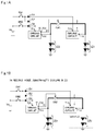
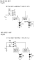
- Fig. 9A is a diagram illustrating a general structural example of a light emitting device including a tail lamp and a stop lamp mounted in the vehicle.
- the light emitting device illustrated in Fig. 9A includes switches SW1 and SW2, diodes D1 to D3, driving circuits 1 and 2, at least one light emitting element (light emitting diode in Fig. 9A ) Z1, and at least one light emitting element (light emitting diode in Fig. 9A ) Z2.
- the light emitting element Z1 is a stop lamp
- the light emitting element Z2 is a tail and stop lamp.
- the switch SW2 becomes ON state so that an input voltage V IN is supplied to the driving circuit 2 via the switch SW2 and the diode D3.
- the driving circuit 2 drives the light emitting element Z2, and the light emitting element Z2 is lighted as illustrated in Fig. 9B .
- the switch SW1 becomes ON state so that the input voltage V IN is supplied to the driving circuit 1 via the switch SW1 and the diode D1 and also is supplied to the driving circuit 2 via the switch SW1 and the diode D2.
- the driving circuit 1 drives the light emitting element Z1 while the driving circuit 2 drives the light emitting element Z2, and hence the light emitting elements Z1 and Z2 are lighted as illustrated in Fig. 9C .
- the light emitting element Z1 is lighted in the stop mode as illustrated in Fig. 9D
- none of the light emitting elements Z1 and Z2 is lighted in the tail mode as illustrated in Fig. 9E .
- the tail lamp is used for informing a driver of a following vehicle that there is a preceding vehicle at night or in a bad weather such as thick fog or snowstorm. Therefore, if none of lamps positioned on the rear of the vehicle is lighted in the tail mode, it is a safety problem.
- the driving circuit 2 and the light emitting element Z2 illustrated in Fig. 9A are divided into two redundant circuits of the tail and stop lamps, which include a set of a driving circuit 2A and a light emitting element Z2A, and a set of a driving circuit 2B and a light emitting element Z2B, as illustrated in Fig. 10 .
- the structure illustrated in Fig. 10 includes more components than the structure illustrated in Fig. 9A , and hence has a problem that power consumption and cost are increased.
- JP-A-2004-34741 proposes a tale/stop lamp having a structure in which each of the tail lamp and the stop lamp is constituted of a plurality of circuits of LEDs so that each of the tail lamp and the stop lamp has redundancy, so as to elongate life of the LEDs by periodic lighting and to light only an unbroken LED when detecting breaking of an LED. Because each of the tail lamp and the stop lamp has redundancy in the tale/stop lamp proposed in JP-A-2004-34741 , the structure has a problem that power consumption and cost are increased, similarly to the structure illustrated in Fig. 10 , as it requires more components than the structure illustrated in Fig. 9A .
- US 5 216 328 A discloses a vehicle lighting system comprising a lighting circuit designed to illuminate a back-up lighting element when a primary lighting element fails. Both lighting elements may be installed in a single housing, such as a headlight assembly. A low-resistance coil is series connected with the primary lighting element. If the primary element fails, the absence of current through the low-resistance coil triggers a switching element to close a mechanical switch and thus to illuminate the back-up element.
- US 2004/0212310 A1 describes a vehicular lamp with a plurality of semiconductor light emitting devices connected in parallel. When a wire of one of the plurality of semiconductor light emitting devices is broken, a current control unit increases an electric current to be supplied to at least one other of the plurality of semiconductor light emitting devices.
- the present invention provides a light emitting element driving device with the features of claim 1, a light emitting device with the features of claim 12 and a vehicle with the features of claim 16.
- Fig. 1A is a diagram illustrating a first structural example of a light emitting device. Note that, in Fig. 1A , the same part as in Fig. 9A is denoted by the same numeral or symbol.
- the light emitting device illustrated in Fig. 1A includes switches SW1 and SW2, diodes D1 to D3, driving circuits 1 and 12, at least one light emitting element (light emitting diode in Fig. 1A ) Z1, and at least one light emitting element (light emitting diode in Fig. 1A ) Z2.
- the driving circuit 1 is, for example, a series regulator arranged to supply constant current to the light emitting element connected to an output terminal T12, a switching regulator arranged to supply predetermined on-duty pulse width modulation (PWM) current to the light emitting element connected to the output terminal T12, or the like.
- the driving circuit 12 is, for example, a series regulator arranged to supply constant current to the light emitting element connected to an output terminal T22, a switching regulator arranged to supply predetermined on-duty PWM current to the light emitting element connected to the output terminal T22, or the like.
- An input voltage V IN is applied to one end of each of the switches SW1 and SW2.
- the other end of the switch SW1 is connected to an input terminal T11 of the driving circuit 1 via a reverse current blocking diode D1 and is connected to an input terminal T21 of the driving circuit 12 via a reverse current blocking diode D2.
- the other end of the switch SW2 is connected to the input terminal T21 of the driving circuit 12 via a reverse current blocking diode D3.
- the switches SW1 and SW2 and the diodes D1 to D3 function as a control portion arranged to control supply of input power to the driving circuits 1 and 12.
- the switch SW1 becomes ON state in a first mode (for example a stop mode). Therefore, in the first mode, the input voltage V IN is supplied to the input terminal T11 of the driving circuit 1 and the input terminal T21 of the driving circuit 12, and hence the driving circuit 1 can supply power to the light emitting element connected to the output terminal T12, while the driving circuit 12 can supply power to the light emitting element connected to the output terminal T22.
- a first mode for example a stop mode
- the switch SW1 becomes OFF state in a mode other than the first mode. Therefore, in a mode other than the first mode, the input voltage V IN is not supplied to the input terminal T11 of the driving circuit 1, and hence the driving circuit 1 cannot supply power to the light emitting element connected to the output terminal T12.
- the switch SW2 becomes ON state in a second mode (for example a tail mode). Therefore, in the second mode, the input voltage V IN is supplied to the input terminal T21 of the driving circuit 12, and hence the driving circuit 12 can supply power to the light emitting element connected to the output terminal T22. Note that it is no problem if there is a state in which the first mode and the second mode are simultaneously active.
- the switch SW2 becomes OFF state in a mode other than the second mode. Therefore, in a mode other than the first mode or the second mode, the input voltage V IN is not supplied to the input terminal T21 of the driving circuit 12, and hence the driving circuit 12 cannot supply power to the light emitting element connected to the output terminal T22.
- the light emitting element Z1 is normally connected to the output terminal T12 of the driving circuit 1, and the light emitting element Z2 is normally connected to the output terminal T22 of the driving circuit 12.
- a bypass path 3 connects the output terminal T12 of the driving circuit 1 to the output terminal T22 of the driving circuit 12.
- a switch SW3 is disposed in the bypass path 3. Therefore, when the switch SW3 is ON state, the bypass path 3 becomes a conductive state. Thus, the output terminal T12 of the driving circuit 1 is connected to the light emitting element Z2, and the output terminal T22 of the driving circuit 12 is connected to the light emitting element Z1. On the other hand, when the switch SW3 is OFF state, the bypass path 3 becomes a cutoff state. Thus, the output terminal T12 of the driving circuit 1 is not connected to the light emitting element Z2, and the output terminal T22 of the driving circuit 12 is not connected to the light emitting element Z1.
- the driving circuit 12 includes an abnormality detection circuit arranged to detect an abnormality of the light emitting element Z2.
- a structural example of the abnormality detection circuit included in the driving circuit 12 is illustrated in Fig. 2 .
- the abnormality detection circuit of the structural example illustrated in Fig. 2 includes comparators 12A and 12C, reference voltage sources 12B and 12D, and an OR gate 12E.
- the comparator 12A compares a voltage at the output terminal T22 with a first reference voltage V REF1 output from the reference voltage source 12B and outputs a high level signal if the voltage at the output terminal T22 is the first reference voltage V REF1 or higher.
- the comparator 12C compares a voltage at the output terminal T22 with a second reference voltage V REF2 (lower than the first reference voltage V REF1 ) output from the reference voltage source 12D, and outputs a high level signal if the voltage at the output terminal T22 is lower than the second reference voltage V REF2 .
- the OR gate 12E sets a signal S1 to the high level, which is output externally from the driving circuit 12 via a terminal T23.
- the first reference voltage V REF1 is set to a value higher than total forward voltage of the light emitting element Z2, for example, to be a threshold value for determining whether or not there is an abnormality that the light emitting element Z2 is not lighted due to its breaking.
- the second reference voltage V REF2 is set to a value lower than a forward voltage of one element in the light emitting element Z2, for example, to be a threshold value for determining whether or not there is an abnormality that the light emitting element Z2 is not lighted due to a ground fault. Note that the setting of the first reference voltage V REF1 and the second reference voltage V REF2 in the above example may be changed so that partial lighting of the light emitting element Z2 can be included in the abnormality of the light emitting element Z2.
- the operation of the light emitting device illustrated in Fig. 1A is described.
- the signal S1 becomes a low level, and the low level signal S1 makes the switch SW3 to OFF state. Therefore, when an abnormality of the light emitting element Z2 is not detected, the light emitting element Z1 emits light in the first mode, while the light emitting element Z2 emits light both in the second mode and in the first mode.
- the signal S1 becomes the high level, and the high level signal S1 makes the switch SW3 to ON state, so that the output terminal T22 of the driving circuit 12 is connected to the light emitting element Z1 via the bypass path 3. Therefore, when an abnormality of the light emitting element Z2 is detected, the light emitting element Z1 emits light both in the first mode and in the second mode as illustrated in Fig. 1B . In other words, even if an abnormality occurs in the light emitting element Z2, it is possible to avoid that none of the light emitting elements is lighted in the second mode.
- the light emitting element Z1 when the light emitting element Z1 is used as a stop lamp disposed at a rear of a vehicle while the light emitting element Z2 is used as a tail and stop lamp disposed at the rear of the vehicle, if an abnormality occurs in the light emitting element Z2, the light emitting element Z1 performs a function as a tail lamp in addition to an original function as a stop lamp. Therefore, it is possible to avoid that none of lamps disposed at the rear of the vehicle in the tail mode, and hence safety is improved.
- Fig. 3 is a diagram illustrating a second structural example of the light emitting device.
- the light emitting device illustrated in Fig. 3 has a structure in which the switches SW1 and SW2 and the diodes D1 to D3 are eliminated from the light emitting device illustrated in Fig. 1 , and the driving circuits 1 and 12 in Fig. 1 are respectively replaced with driving circuits 1' and 12'.
- the input voltage V IN is directly applied to the input terminal T11 of the driving circuit 1' and the input terminal T21 of the driving circuit 12'.
- the driving circuit 1' has a structure in which an enable terminal T13 is added to the driving circuit 1 so as to have an enable function.
- the driving circuit 1' becomes an enabled state when an enable signal EN11 is supplied to the enable terminal T13, while it becomes a disabled state when the enable signal EN11 is not supplied to the enable terminal T13.
- a voltage generation circuit disposed in the driving circuit 1' so as to generate an internal power supply voltage becomes an active state when the enable signal EN11 is supplied to the enable terminal T13, while it becomes a non-active state when the enable signal EN11 is not supplied to the enable terminal T13.
- the driving circuit 12' has a structure in which an enable terminal T24 is added to the driving circuit 12 so as to have an enable function.
- the driving circuit 12' becomes an enabled state when an enable signal EN12 is supplied to the enable terminal T24, while it becomes a disabled state when the enable signal EN12 is not supplied to the enable terminal T24.
- a voltage generation circuit disposed in the driving circuit 12' so as to generate an internal power supply voltage becomes an active state when the enable signal EN12 is supplied to the enable terminal T24, while it becomes a non-active state when the enable signal EN12 is not supplied to the enable terminal T24.
- the driving circuit 1' when the enable signal EN 11 is supplied to the enable terminal T13 of the driving circuit 1', the driving circuit 1' can supply power to the light emitting element connected to the output terminal T12. Further, when the enable signal EN12 is supplied to the enable terminal T24 of the driving circuit 12', the driving circuit 12' can supply power to the light emitting element connected to the output terminal T22.
- the enable signal EN11 is not supplied to the enable terminal T13 of the driving circuit 1', and hence the driving circuit 1' cannot supply power to the light emitting element connected to the output terminal T12.
- the driving circuit 12' when the enable signal EN12 is supplied to the enable terminal T24 of the driving circuit 12', the driving circuit 12' can supply power to the light emitting element connected to the output terminal T22.
- the enable signal EN12 is not supplied to the enable terminal T24 of the driving circuit 12'. Therefore, in a mode other than the first mode or the second mode, because the enable signal EN12 is not supplied to the enable terminal T24 of the driving circuit 12', the driving circuit 12' cannot supply power to the light emitting element connected to the output terminal T22.
- the light emitting device illustrated in Fig. 3 can eliminate the discrete components (the switches SW1 and SW2 and the diodes D1 to D3), it is possible to achieve a lower cost and a smaller size than the light emitting device illustrated in Fig. 1 .
- Fig. 4 is a diagram illustrating a third structural example of the light emitting device.
- the light emitting device illustrated in Fig. 4 has a structure in which a switch SW4 is added to the light emitting device illustrated in Fig. 1 , and the driving circuit 1 is replaced with a driving circuit 11.
- the switch SW4 is disposed in the bypass path 3 and is connected in parallel to the switch SW3.
- the driving circuit 11 has a structure in which the abnormality detection circuit arranged to detect an abnormality of the light emitting element Z1 is added to the driving circuit 1.
- the driving circuit 11 includes the abnormality detection circuit arranged to detect an abnormality of the light emitting element Z1.
- a structural example of the abnormality detection circuit disposed in the driving circuit 11 has a structure in which the terminal T22 in the structure illustrated in Fig. 2 is replaced with the terminal T12, and the terminal T23 is replaced with a terminal T14, from which a signal S2 is output.
- the first reference voltage V REF1 is set to a value higher than total forward voltage of the light emitting element Z1, for example, to be a threshold value for determining whether or not there is an abnormality that the light emitting element Z1 is not lighted due to its breaking.
- the second reference voltage V REF2 is set to a value lower than a forward voltage of one element in the light emitting element Z1, for example, to be a threshold value for determining whether or not there is an abnormality that the light emitting element Z1 is not lighted due to a ground fault. Note that the setting of the first reference voltage V REF1 and the second reference voltage V REF2 in the above example may be changed so that partial lighting of the light emitting element Z1 can be included in the abnormality of the light emitting element Z1 .
- the operation of the light emitting device illustrated in Fig. 4 is described.
- the signal S2 becomes the low level, and the low level signal S2 makes the switch SW4 to OFF state. Therefore, when an abnormality of the light emitting elements Z1 and Z2 is not detected, the light emitting element Z1 emits light in the first mode, while the light emitting element Z2 emits light both in the second mode and in the first mode.
- the signal S1 becomes the high level, and the high level signal S1 makes the switch SW3 to ON state, so that the output terminal T22 of the driving circuit 12 is connected to the light emitting element Z1 via the bypass path 3. Therefore, when an abnormality of the light emitting element Z2 is detected, the light emitting element Z1 emits light both in the first mode and in the second mode. In other words, even if an abnormality occurs in the light emitting element Z2, it is possible to avoid that none of the light emitting elements is lighted in the second mode.
- the signal S2 becomes the high level, and the high level signal S2 makes the switch SW4 to ON state, so that the output terminal T12 of the driving circuit 11 is connected to the light emitting element Z2 via the bypass path 3. Therefore, when an abnormality of the light emitting element Z1 is detected, the light emitting element Z2 emits light in the second mode.
- the first mode current is supplied from both the driving circuits 11 and 12, and therefore the light emitting element Z2 emits light with higher luminance than the second mode.
- the first mode and the second mode can be easily discriminated from each other based on the light emission state of the light emitting element Z2.
- Fig. 5 is a diagram illustrating a fourth structural example of the light emitting device.
- the light emitting device illustrated in Fig. 5 has a structure in which the switches SW3 and SW4 of the light emitting device illustrated in Fig. 4 are integrated so that only the switch SW3 is left, and an OR gate 4 that outputs a logical OR of the signal S1 and the signal S2 is added. ON state and OFF state of the switch SW3 are switched by the output signal of the OR gate 4.
- the light emitting device illustrated in Fig. 5 produces the same effect as the light emitting device illustrated in Fig. 4 .
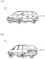
- the light emitting device described above can be appropriately used as a tail lamp (appropriately including a side lamp and a back lamp) X11 and a stop lamp X12, for example, as illustrated in Figs. 6 and 7 .
- the light emitting device described above may be provided as an LED rear lamp module Y10 illustrated in Fig. 8 .
- it may be provided in a form of the light emitting element driving device in which the light emitting elements Z1 and Z2 are eliminated from the light emitting device described above.
- the present invention is not limited to this structure.
- an organic electro-luminescence (EL) element as the light emitting element.
- the diode D2 may be eliminated in the first, third, and fourth structural examples.
- the light emitting element Z2 is used not as the tail and stop lamp but as the tail lamp, for example.
- the abnormality detection circuit disposed in the driving circuit 12 may perform the detection operation only in the second mode.
- the abnormality detection circuit disposed in the driving circuit 11 may perform the detection operation only in the first mode.
- the light emitting element driving device described above includes a first driving circuit arranged to be capable of supplying power to a light emitting element connected to an output terminal in a first mode, and to be disabled to supply power to the light emitting element connected to the output terminal in a mode other than the first mode, a second driving circuit arranged to be capable of supplying power to a light emitting element connected to an output terminal in a second mode, a first abnormality detecting portion arranged to detect an abnormality of the light emitting element normally connected to the output terminal of the second driving circuit at least in the second mode, a bypass path connecting the output terminal of the first driving circuit to the output terminal of the second driving circuit, and a first switching portion disposed in the bypass path so as to make the bypass path into a conductive state when an abnormality is detected by the first abnormality detecting portion, and to make the bypass path into a cutoff state when an abnormality is not detected by the first abnormality detecting portion (first structure).
- the light emitting element driving device of the first structure described above may have a structure, in which the second driving circuit is capable of supplying power to the light emitting element connected to the output terminal in the first mode and is disabled to supply power to the light emitting element connected to the output terminal in a mode other than the first mode or the second mode (second structure).
- the light emitting element driving device of the first or second structure described above may further include a control portion arranged to control supply of input power to the first driving circuit and the second driving circuit, in which the control portion supplies the input power to the first driving circuit in the first mode and does not supply the input power to the first driving circuit in a mode other than the first mode, while the control portion supplies the input power to the second driving circuit in the second mode (third structure).
- the light emitting element driving device of the third structure described above may have a structure, in which the control portion supplies the input power to the second driving circuit in the first mode and does not supply the input power to the second driving circuit in a mode other than the first mode or the second mode (fourth structure).
- the light emitting element driving device of the first or second structure described above may have a structure, in which the first driving circuit becomes an enabled state in the first mode and becomes a disabled state in a mode other than the first mode, and the second driving circuit becomes an enabled state in the second mode (fifth structure).
- the light emitting element driving device of the fifth structure described above may have a structure, in which the second driving circuit becomes an enabled state in the first mode and becomes a disabled state in a mode other than the first mode or the second mode (sixth structure).
- the light emitting element driving device of the fifth or sixth structure described above may further include a second abnormality detecting portion arranged to detect an abnormality of the light emitting element normally connected to the output terminal of the first driving circuit at least in the first mode, and a second switching portion disposed in the bypass path so as to make the bypass path into a conductive state when an abnormality is detected by the second abnormality detecting portion, and to make the bypass path into a cutoff state when an abnormality is not detected by the second abnormality detecting portion (seventh structure).
- a second abnormality detecting portion arranged to detect an abnormality of the light emitting element normally connected to the output terminal of the first driving circuit at least in the first mode
- a second switching portion disposed in the bypass path so as to make the bypass path into a conductive state when an abnormality is detected by the second abnormality detecting portion, and to make the bypass path into a cutoff state when an abnormality is not detected by the second abnormality detecting portion (seventh structure).
- the light emitting device described above includes the light emitting element driving device according to any one of the first to seventh structures, a first light emitting element normally connected to the output terminal of the first driving circuit, and a second light emitting element normally connected to the output terminal of the second driving circuit (eighth structure).
- the light emitting device of the eighth structure described above may have a structure in which each of the first light emitting element and the second light emitting element is a light emitting diode or an organic EL element (ninth structure).
- the light emitting device of the eighth or ninth structure described above may have a structure in which the first light emitting element is used as a stop lamp, and the second light emitting element is used as a tail lamp or a tail and stop lamp (tenth structure).
- the light emitting device of the tenth structure described above may have a structure in which the light emitting device is mounted as a rear lamp module in a vehicle (eleventh structure).
- the vehicle described above includes the light emitting device according to the eighth or ninth structure (twelfth structure).
Landscapes
- Engineering & Computer Science (AREA)
- Mechanical Engineering (AREA)
- Lighting Device Outwards From Vehicle And Optical Signal (AREA)
- Circuit Arrangement For Electric Light Sources In General (AREA)
Claims (16)
- Ansteuerungsvorrichtung für lichtemittierendes Element, umfassend:eine erste Treiberschaltung (11), die dafür ausgelegt ist, einem lichtemittierenden Element (Z1), das mit einem Ausgangsanschluss der ersten Treiberschaltung (11) verbunden ist, in einem ersten Modus Strom zuführen zu können, und in einem anderen Modus als dem ersten Modus deaktiviert werden zu können, um dem lichtemittierenden Element, das mit dem Ausgangsanschluss der ersten Treiberschaltung (11) verbunden ist, Strom zuzuführen;dadurch gekennzeichnet, dass sie Folgendes umfasst:eine zweite Treiberschaltung (12), die dafür ausgelegt ist, einem lichtemittierenden Element (Z2), das mit einem Ausgangsanschluss der zweiten Treiberschaltung (12) verbunden ist, in einem zweiten Modus Strom zuführen zu können;eine erste Anomaliedetektionsschaltung, die dafür ausgelegt ist, eine Anomalie des lichtemittierenden Elements (Z2), das mit dem Ausgangsanschluss der zweiten Treiberschaltung (12) verbunden ist, mindestens im zweiten Modus zu detektieren;einen Umgehungspfad (3), der den Ausgangsanschluss der ersten Treiberschaltung (11) mit dem Ausgangsanschluss der zweiten Treiberschaltung (12) zu verbinden; undeinen ersten Schaltabschnitt, der in dem Umgehungspfad (3) angeordnet ist, um:- den Umgehungspfad (3) in einen leitfähigen Zustand zu versetzen, um das lichtemittierende Element (Z1), das mit dem Ausgangsanschluss der ersten Treiberschaltung (11) verbunden ist, und den Ausgangsanschluss der zweiten Treiberschaltung (12) miteinander zu verbinden, wenn durch die erste Anomaliedetektionsschaltung eine Anomalie detektieren wird, und- den Umgehungspfad (3) in einen Abschaltzustand zu versetzen, um das lichtemittierende Element (Z1), das mit dem Ausgangsanschluss der ersten Treiberschaltung (11) verbunden ist, und den Ausgangsanschluss der zweiten Treiberschaltung (12) nicht miteinander zu verbinden, wenn durch die erste Anomaliedetektionsschaltung keine Anomalie detektieren wird, undwobei die erste Treiberschaltung (11) in der Lage ist, dem lichtemittierenden Element, das mit dem Ausgangsanschluss der ersten Treiberschaltung (11) verbunden ist, im ersten Modus Strom zuzuführen, selbst wenn sich der Umgehungspfad (3) im Abschaltzustand befindet.
- Ansteuerungsvorrichtung für lichtemittierendes Element nach Anspruch 1, des Weiteren umfassend:eine zweite Anomaliedetektionsschaltung, die dafür ausgelegt ist, eine Anomalie des lichtemittierenden Elements (Z1), das mit dem Ausgangsanschluss der ersten Treiberschaltung (11) verbunden ist, mindestens im ersten Modus zu detektieren;- wobei der erste Schaltabschnitt den Umgehungspfad (3) in den leitfähigen Zustand versetzt, um die Ausgangsanschlüsse der ersten Treiberschaltung (11) und der zweiten Treiberschaltung (12) miteinander zu verbinden, wenn eine Anomalie durch die zweite Anomaliedetektionsschaltung detektiert wird, undden Umgehungspfad (3) in einen Abschaltzustand versetzt, um die Ausgangsanschlüsse der ersten Treiberschaltung (11) und der zweiten Treiberschaltung (12) nicht miteinander zu verbinden, wenn auch durch die zweite Anomaliedetektionsschaltung keine Anomalie detektiert wird.
- Ansteuerungsvorrichtung für lichtemittierendes Element nach Anspruch 2, dadurch gekennzeichnet, dass die zweite Treiberschaltung (12) in der Lage ist, dem lichtemittierenden Element (Z2), das mit dem Ausgangsanschluss der zweiten Treiberschaltung (12) verbunden ist, im ersten Modus Strom zuzuführen, und in einem anderen Modus als dem ersten Modus oder dem zweiten Modus deaktiviert ist, um dem lichtemittierenden Element, das mit dem Ausgangsanschluss der zweiten Treiberschaltung (12) verbunden ist, keinen Strom zuführen zu können.
- Ansteuerungsvorrichtung für lichtemittierendes Element nach Anspruch 2 oder 3, des Weiteren umfassend einen Steuerungsabschnitt, der dafür ausgelegt ist, die Zufuhr von Eingangsleistung zu der ersten Treiberschaltung (11) und der zweiten Treiberschaltung (12) zu steuern, dadurch gekennzeichnet, dass
der Steuerungsabschnitt im ersten Modus die Eingangsleistung in die erste Treiberschaltung (11) einspeist und in einem anderen Modus als dem ersten Modus keine Eingangsleistung in die erste Treiberschaltung (11) einspeist, während der Steuerungsabschnitt im zweiten Modus die Eingangsleistung in die zweite Treiberschaltung (12) einspeist. - Ansteuerungsvorrichtung für lichtemittierendes Element nach Anspruch 4, dadurch gekennzeichnet, dass der Steuerungsabschnitt die Eingangsleistung im ersten Modus in die zweite Treiberschaltung (12) einspeist und in einem anderen Modus als dem ersten oder dem zweiten Modus keine Eingangsleistung in die zweite Treiberschaltung (12) einspeist.
- Ansteuerungsvorrichtung für lichtemittierendes Element nach Anspruch 2 oder 3, dadurch gekennzeichnet, dass die erste Treiberschaltung (11) im ersten Modus in einen aktivierten Zustand übergeht und in einem anderen Modus als dem ersten Modus in einen deaktivierten Zustand übergeht, und
die zweite Treiberschaltung (12) im zweiten Modus in einen aktivierten Zustand übergeht. - Ansteuerungsvorrichtung für lichtemittierendes Element nach Anspruch 6, dadurch gekennzeichnet, dass die zweite Treiberschaltung (12) im ersten Modus in einen aktivierten Zustand übergeht und in einem anderen Modus als dem ersten oder dem zweiten Modus in einen deaktivierten Zustand übergeht.
- Ansteuerungsvorrichtung für lichtemittierendes Element nach Anspruch 1, des Weiteren umfassend:eine zweite Anomaliedetektionsschaltung, die dafür ausgelegt ist, eine Anomalie des lichtemittierenden Elements (Z1), das mit dem Ausgangsanschluss der ersten Treiberschaltung (11) verbunden ist, mindestens im ersten Modus zu detektieren; undeinen zweiten Schaltabschnitt, der in dem Umgehungspfad angeordnet ist, um:- den Umgehungspfad (3) in den leitfähigen Zustand zu versetzen, um die Ausgangsanschlüsse der ersten Treiberschaltung (11) und der zweiten Treiberschaltung (12) miteinander zu verbinden, wenn eine Anomalie durch die zweite Anomaliedetektionsschaltung detektiert wird, und- den Umgehungspfad (3) in einen Abschaltzustand zu versetzen, um die Ausgangsanschlüsse der ersten Treiberschaltung (11) und der zweiten Treiberschaltung (12) nicht miteinander zu verbinden, wenn durch die zweite Anomaliedetektionsschaltung keine Anomalie detektiert wird.
- Ansteuerungsvorrichtung für lichtemittierendes Element nach Anspruch 1, des Weiteren umfassend:eine zweite Anomaliedetektionsschaltung, die dafür ausgelegt ist, eine Anomalie des lichtemittierenden Elements (Z1), das mit dem Ausgangsanschluss der ersten Treiberschaltung (11) verbunden ist, mindestens im ersten Modus zu detektieren; undeine ODER-Schaltung, die dafür ausgelegt ist, ein logisches ODER von Ausgängen der ersten und der zweiten Anomalie-Erkennungsschaltung auszugeben,wobei der erste Schaltabschnitt durch einen Ausgang der ODER-Schaltung gesteuert wird.
- Ansteuerungsvorrichtung für lichtemittierendes Element nach Anspruch 1 oder 9, wobei, wenn sich der Umgehungspfad (3) im leitfähigen Zustand befindet, das lichtemittierende Element (Z1), das mit dem Ausgangsanschluss der ersten Treiberschaltung (11) verbunden ist, und das lichtemittierende Element (Z2), das mit dem Ausgangsanschluss der zweiten Treiberschaltung (12) verbunden ist, zueinander parallel geschaltet werden.
- Ansteuerungsvorrichtung für lichtemittierendes Element nach einem der Ansprüche 1, 9 und 10, umfassend:einen Steuerungsabschnitt, der dafür ausgelegt ist, die Eingangsleistung in die erste Treiberschaltung (11) und die zweite Treiberschaltung (12) zu steuern,wobei der Steuerungsabschnitt Folgendes umfasst:einen ersten Modusschalter, der sich im ersten Modus in einem EIN-Zustand befindet,einen zweiten Modusschalter, der sich im zweiten Modus in einem EIN-Zustand befindet,eine erste Diode,eine zweite Diode undeine dritte Diode,wobei eine Eingangsspannung an ein Ende des ersten Modusschalters angelegt wird und an ein Ende des zweiten Modusschalters angelegt wird,das andere Ende des ersten Modusschalters über die erste Diode mit einem Eingangsanschluss der ersten Treiberschaltung (11) verbunden ist und über die zweite Diode mit einem Eingangsanschluss der zweiten Treiberschaltung (12) verbunden ist, unddas andere Ende des zweiten Modusschalters über die dritte Diode mit dem Eingangsanschluss der zweiten Treiberschaltung (12) verbunden ist.
- Leuchtvorrichtung, umfassend:die Ansteuerungsvorrichtung für lichtemittierendes Element nach einem der Ansprüche 1 bis 11;ein erstes lichtemittierendes Element (Z1), das mit dem Ausgangsanschluss der ersten Treiberschaltung (11) verbunden ist; undein zweites lichtemittierendes Element (Z2), das mit dem Ausgangsanschluss der zweiten Treiberschaltung (12) verbunden ist.
- Leuchtvorrichtung nach Anspruch 12, dadurch gekennzeichnet, dass sowohl das erste lichtemittierende Element (Z1) als auch das zweite lichtemittierende Element (Z2) eine Leuchtdiode oder ein organisches EL-Element ist.
- Leuchtvorrichtung nach Anspruch 12 oder 13, dadurch gekennzeichnet, dass
das erste lichtemittierende Element (Z1) als Bremsleuchte verwendet wird und
das zweite lichtemittierende Element (Z2) als Schlussleuchte oder als Schluss- und Bremsleuchte verwendet wird. - Leuchtvorrichtung nach Anspruch 14, dadurch gekennzeichnet, dass die Leuchtvorrichtung als Rückleuchtenmodul in einem Fahrzeug montiert ist.
- Fahrzeug, umfassend die Leuchtvorrichtung nach Anspruch 14 oder 15.
Applications Claiming Priority (1)
| Application Number | Priority Date | Filing Date | Title |
|---|---|---|---|
| JP2016055482A JP6757579B2 (ja) | 2016-03-18 | 2016-03-18 | 発光素子駆動装置、発光装置、車両 |
Publications (2)
| Publication Number | Publication Date |
|---|---|
| EP3220719A1 EP3220719A1 (de) | 2017-09-20 |
| EP3220719B1 true EP3220719B1 (de) | 2020-05-06 |
Family
ID=58401391
Family Applications (1)
| Application Number | Title | Priority Date | Filing Date |
|---|---|---|---|
| EP17161612.1A Active EP3220719B1 (de) | 2016-03-18 | 2017-03-17 | Ansteuerungsvorrichtung für lichtemittierendes element, lichtemittierende vorrichtung und fahrzeug |
Country Status (4)
| Country | Link |
|---|---|
| US (1) | US10053008B2 (de) |
| EP (1) | EP3220719B1 (de) |
| JP (1) | JP6757579B2 (de) |
| CN (1) | CN107205295B (de) |
Families Citing this family (11)
| Publication number | Priority date | Publication date | Assignee | Title |
|---|---|---|---|---|
| DE112018006777B4 (de) | 2018-01-05 | 2022-06-15 | Rohm Co., Ltd. | Vielfach-abgabe-last-treibereinrichtung |
| JP7053967B2 (ja) * | 2019-03-28 | 2022-04-12 | シグニファイ ホールディング ビー ヴィ | クラス2の回路保護 |
| US10841998B1 (en) * | 2019-05-17 | 2020-11-17 | Signify Holding B.V. | Shared power topology for LED luminaires |
| CN110356316A (zh) * | 2019-06-28 | 2019-10-22 | 潍柴动力股份有限公司 | 车灯控制系统 |
| CN110197638A (zh) * | 2019-06-28 | 2019-09-03 | 上海天马有机发光显示技术有限公司 | 一种显示面板、显示装置和显示面板的驱动方法 |
| CN110957896B (zh) * | 2019-08-07 | 2022-03-29 | 河南嘉晨智能控制股份有限公司 | 一种便于检测的多个mosfet管并联电路 |
| TWI728749B (zh) * | 2020-03-16 | 2021-05-21 | 友達光電股份有限公司 | 發光模組及其修補方法 |
| CN111956821B (zh) * | 2020-07-15 | 2021-11-09 | 浙江阳光照明电器集团股份有限公司 | 一种紫外杀菌灯杀菌方法及电路 |
| US11987178B2 (en) * | 2020-12-21 | 2024-05-21 | Valeo Vision | Light assembly with a fail safe mode for a low beam function |
| US11718220B2 (en) * | 2021-01-19 | 2023-08-08 | Infineon Technologies Ag | Compensating for failed pixels in pixelated vehicle headlamps |
| TWI894999B (zh) * | 2024-06-07 | 2025-08-21 | 友達光電股份有限公司 | 微型發光二極體面板、操作方法與畫素補償電路 |
Family Cites Families (11)
| Publication number | Priority date | Publication date | Assignee | Title |
|---|---|---|---|---|
| JPS5432462Y2 (de) * | 1975-01-29 | 1979-10-08 | ||
| JPH0760753B2 (ja) | 1987-12-07 | 1995-06-28 | 林時計工業株式会社 | 照明装置 |
| US5216328A (en) | 1991-10-30 | 1993-06-01 | Lu Tan T | Vehicle lighting system |
| JPH0544686U (ja) * | 1991-11-21 | 1993-06-15 | 市光工業株式会社 | リヤーコンビネーシヨンランプの点灯回路 |
| JPH0761285A (ja) * | 1993-08-25 | 1995-03-07 | Toyota Motor Corp | 車両用後部灯火制御装置 |
| JPH10982A (ja) * | 1996-06-17 | 1998-01-06 | Harness Sogo Gijutsu Kenkyusho:Kk | 自動車用ランプ制御装置 |
| JP2004034741A (ja) * | 2002-06-28 | 2004-02-05 | Matsushita Electric Works Ltd | 車載用のテール/ストップランプ |
| JP2004136719A (ja) * | 2002-10-15 | 2004-05-13 | Koito Mfg Co Ltd | 点灯回路 |
| JP4094477B2 (ja) * | 2003-04-28 | 2008-06-04 | 株式会社小糸製作所 | 車両用灯具 |
| US7040790B2 (en) * | 2004-05-25 | 2006-05-09 | Ledtronics, Inc. | Two circuit LED light bulb |
| DE102004038425A1 (de) | 2004-08-07 | 2005-11-24 | Daimlerchrysler Ag | Fahrzeugbeleuchtungssystem und zugehöriges Verfahren zur Notbeleuchtung |
-
2016
- 2016-03-18 JP JP2016055482A patent/JP6757579B2/ja active Active
-
2017
- 2017-03-14 CN CN201710150427.3A patent/CN107205295B/zh active Active
- 2017-03-14 US US15/458,310 patent/US10053008B2/en active Active
- 2017-03-17 EP EP17161612.1A patent/EP3220719B1/de active Active
Non-Patent Citations (1)
| Title |
|---|
| None * |
Also Published As
| Publication number | Publication date |
|---|---|
| JP6757579B2 (ja) | 2020-09-23 |
| EP3220719A1 (de) | 2017-09-20 |
| US10053008B2 (en) | 2018-08-21 |
| US20170267174A1 (en) | 2017-09-21 |
| CN107205295A (zh) | 2017-09-26 |
| JP2017165384A (ja) | 2017-09-21 |
| CN107205295B (zh) | 2019-02-19 |
Similar Documents
| Publication | Publication Date | Title |
|---|---|---|
| EP3220719B1 (de) | Ansteuerungsvorrichtung für lichtemittierendes element, lichtemittierende vorrichtung und fahrzeug | |
| US10360969B2 (en) | Light emitting element driving semiconductor integrated circuit, light emitting element driving device, light emitting device, and vehicle | |
| US10327290B2 (en) | Lighting circuit and vehicle lamp | |
| US10081301B2 (en) | Lighting circuit and vehicular turn signal lamp | |
| EP3244700B1 (de) | Erdschlussdetektorschaltung, fehlererkennungsschaltung, lichtemittierende vorrichtung, fahrzeug | |
| US9621024B2 (en) | Power supply device supplying limited DC power to load based on ground fault detection | |
| US7964987B2 (en) | Light emitting apparatus | |
| JP5739747B2 (ja) | 半導体光源点灯回路 | |
| US9162607B2 (en) | Vehicular lamp | |
| JP6461955B2 (ja) | 発光ダイオードデバイス | |
| US11051383B2 (en) | Ground fault detection circuit, abnormality detection circuit, light emitting device, vehicle | |
| JP5280182B2 (ja) | 車両用灯具 | |
| JP2023101804A (ja) | ランプ制御装置 | |
| JP2015081000A (ja) | 車両用灯具 | |
| WO2023106199A1 (ja) | 点灯回路、及び車両用灯具 | |
| JP7393414B2 (ja) | 車両用灯具および点灯回路 | |
| KR101903970B1 (ko) | 차량 led 램프의 텔-테일 회로 | |
| EP4122766A1 (de) | Lichtquellenmodul und beleuchtungsschaltung | |
| US11970109B2 (en) | Electronic device and automotive lighting device | |
| JP2025080399A (ja) | 点灯モジュール | |
| WO2024079980A1 (ja) | 半導体装置、発光装置、車両 | |
| CN118370004A (zh) | 点亮电路及车辆用灯具 | |
| CN116803211A (zh) | 具有用于近光功能的故障安全模式的照明组件 | |
| JP2015080999A (ja) | 車両用灯具 | |
| JP2008130990A (ja) | 断線検出方法 |
Legal Events
| Date | Code | Title | Description |
|---|---|---|---|
| PUAI | Public reference made under article 153(3) epc to a published international application that has entered the european phase |
Free format text: ORIGINAL CODE: 0009012 |
|
| STAA | Information on the status of an ep patent application or granted ep patent |
Free format text: STATUS: THE APPLICATION HAS BEEN PUBLISHED |
|
| AK | Designated contracting states |
Kind code of ref document: A1 Designated state(s): AL AT BE BG CH CY CZ DE DK EE ES FI FR GB GR HR HU IE IS IT LI LT LU LV MC MK MT NL NO PL PT RO RS SE SI SK SM TR |
|
| AX | Request for extension of the european patent |
Extension state: BA ME |
|
| STAA | Information on the status of an ep patent application or granted ep patent |
Free format text: STATUS: REQUEST FOR EXAMINATION WAS MADE |
|
| 17P | Request for examination filed |
Effective date: 20180316 |
|
| RBV | Designated contracting states (corrected) |
Designated state(s): AL AT BE BG CH CY CZ DE DK EE ES FI FR GB GR HR HU IE IS IT LI LT LU LV MC MK MT NL NO PL PT RO RS SE SI SK SM TR |
|
| STAA | Information on the status of an ep patent application or granted ep patent |
Free format text: STATUS: EXAMINATION IS IN PROGRESS |
|
| 17Q | First examination report despatched |
Effective date: 20190417 |
|
| REG | Reference to a national code |
Ref country code: DE Ref legal event code: R079 Ref document number: 602017015963 Country of ref document: DE Free format text: PREVIOUS MAIN CLASS: H05B0033080000 Ipc: H05B0047290000 |
|
| GRAP | Despatch of communication of intention to grant a patent |
Free format text: ORIGINAL CODE: EPIDOSNIGR1 |
|
| STAA | Information on the status of an ep patent application or granted ep patent |
Free format text: STATUS: GRANT OF PATENT IS INTENDED |
|
| RIC1 | Information provided on ipc code assigned before grant |
Ipc: H05B 47/29 20200101AFI20200129BHEP |
|
| INTG | Intention to grant announced |
Effective date: 20200219 |
|
| GRAS | Grant fee paid |
Free format text: ORIGINAL CODE: EPIDOSNIGR3 |
|
| GRAA | (expected) grant |
Free format text: ORIGINAL CODE: 0009210 |
|
| STAA | Information on the status of an ep patent application or granted ep patent |
Free format text: STATUS: THE PATENT HAS BEEN GRANTED |
|
| AK | Designated contracting states |
Kind code of ref document: B1 Designated state(s): AL AT BE BG CH CY CZ DE DK EE ES FI FR GB GR HR HU IE IS IT LI LT LU LV MC MK MT NL NO PL PT RO RS SE SI SK SM TR |
|
| REG | Reference to a national code |
Ref country code: GB Ref legal event code: FG4D |
|
| REG | Reference to a national code |
Ref country code: CH Ref legal event code: EP Ref country code: AT Ref legal event code: REF Ref document number: 1268951 Country of ref document: AT Kind code of ref document: T Effective date: 20200515 |
|
| REG | Reference to a national code |
Ref country code: IE Ref legal event code: FG4D |
|
| REG | Reference to a national code |
Ref country code: DE Ref legal event code: R096 Ref document number: 602017015963 Country of ref document: DE |
|
| REG | Reference to a national code |
Ref country code: LT Ref legal event code: MG4D |
|
| REG | Reference to a national code |
Ref country code: NL Ref legal event code: MP Effective date: 20200506 |
|
| PG25 | Lapsed in a contracting state [announced via postgrant information from national office to epo] |
Ref country code: GR Free format text: LAPSE BECAUSE OF FAILURE TO SUBMIT A TRANSLATION OF THE DESCRIPTION OR TO PAY THE FEE WITHIN THE PRESCRIBED TIME-LIMIT Effective date: 20200807 Ref country code: NO Free format text: LAPSE BECAUSE OF FAILURE TO SUBMIT A TRANSLATION OF THE DESCRIPTION OR TO PAY THE FEE WITHIN THE PRESCRIBED TIME-LIMIT Effective date: 20200806 Ref country code: FI Free format text: LAPSE BECAUSE OF FAILURE TO SUBMIT A TRANSLATION OF THE DESCRIPTION OR TO PAY THE FEE WITHIN THE PRESCRIBED TIME-LIMIT Effective date: 20200506 Ref country code: LT Free format text: LAPSE BECAUSE OF FAILURE TO SUBMIT A TRANSLATION OF THE DESCRIPTION OR TO PAY THE FEE WITHIN THE PRESCRIBED TIME-LIMIT Effective date: 20200506 Ref country code: IS Free format text: LAPSE BECAUSE OF FAILURE TO SUBMIT A TRANSLATION OF THE DESCRIPTION OR TO PAY THE FEE WITHIN THE PRESCRIBED TIME-LIMIT Effective date: 20200906 Ref country code: SE Free format text: LAPSE BECAUSE OF FAILURE TO SUBMIT A TRANSLATION OF THE DESCRIPTION OR TO PAY THE FEE WITHIN THE PRESCRIBED TIME-LIMIT Effective date: 20200506 Ref country code: PT Free format text: LAPSE BECAUSE OF FAILURE TO SUBMIT A TRANSLATION OF THE DESCRIPTION OR TO PAY THE FEE WITHIN THE PRESCRIBED TIME-LIMIT Effective date: 20200907 |
|
| PG25 | Lapsed in a contracting state [announced via postgrant information from national office to epo] |
Ref country code: BG Free format text: LAPSE BECAUSE OF FAILURE TO SUBMIT A TRANSLATION OF THE DESCRIPTION OR TO PAY THE FEE WITHIN THE PRESCRIBED TIME-LIMIT Effective date: 20200806 Ref country code: RS Free format text: LAPSE BECAUSE OF FAILURE TO SUBMIT A TRANSLATION OF THE DESCRIPTION OR TO PAY THE FEE WITHIN THE PRESCRIBED TIME-LIMIT Effective date: 20200506 Ref country code: LV Free format text: LAPSE BECAUSE OF FAILURE TO SUBMIT A TRANSLATION OF THE DESCRIPTION OR TO PAY THE FEE WITHIN THE PRESCRIBED TIME-LIMIT Effective date: 20200506 Ref country code: HR Free format text: LAPSE BECAUSE OF FAILURE TO SUBMIT A TRANSLATION OF THE DESCRIPTION OR TO PAY THE FEE WITHIN THE PRESCRIBED TIME-LIMIT Effective date: 20200506 |
|
| REG | Reference to a national code |
Ref country code: AT Ref legal event code: MK05 Ref document number: 1268951 Country of ref document: AT Kind code of ref document: T Effective date: 20200506 |
|
| PG25 | Lapsed in a contracting state [announced via postgrant information from national office to epo] |
Ref country code: NL Free format text: LAPSE BECAUSE OF FAILURE TO SUBMIT A TRANSLATION OF THE DESCRIPTION OR TO PAY THE FEE WITHIN THE PRESCRIBED TIME-LIMIT Effective date: 20200506 Ref country code: AL Free format text: LAPSE BECAUSE OF FAILURE TO SUBMIT A TRANSLATION OF THE DESCRIPTION OR TO PAY THE FEE WITHIN THE PRESCRIBED TIME-LIMIT Effective date: 20200506 |
|
| PG25 | Lapsed in a contracting state [announced via postgrant information from national office to epo] |
Ref country code: ES Free format text: LAPSE BECAUSE OF FAILURE TO SUBMIT A TRANSLATION OF THE DESCRIPTION OR TO PAY THE FEE WITHIN THE PRESCRIBED TIME-LIMIT Effective date: 20200506 Ref country code: DK Free format text: LAPSE BECAUSE OF FAILURE TO SUBMIT A TRANSLATION OF THE DESCRIPTION OR TO PAY THE FEE WITHIN THE PRESCRIBED TIME-LIMIT Effective date: 20200506 Ref country code: EE Free format text: LAPSE BECAUSE OF FAILURE TO SUBMIT A TRANSLATION OF THE DESCRIPTION OR TO PAY THE FEE WITHIN THE PRESCRIBED TIME-LIMIT Effective date: 20200506 Ref country code: SM Free format text: LAPSE BECAUSE OF FAILURE TO SUBMIT A TRANSLATION OF THE DESCRIPTION OR TO PAY THE FEE WITHIN THE PRESCRIBED TIME-LIMIT Effective date: 20200506 Ref country code: IT Free format text: LAPSE BECAUSE OF FAILURE TO SUBMIT A TRANSLATION OF THE DESCRIPTION OR TO PAY THE FEE WITHIN THE PRESCRIBED TIME-LIMIT Effective date: 20200506 Ref country code: CZ Free format text: LAPSE BECAUSE OF FAILURE TO SUBMIT A TRANSLATION OF THE DESCRIPTION OR TO PAY THE FEE WITHIN THE PRESCRIBED TIME-LIMIT Effective date: 20200506 Ref country code: AT Free format text: LAPSE BECAUSE OF FAILURE TO SUBMIT A TRANSLATION OF THE DESCRIPTION OR TO PAY THE FEE WITHIN THE PRESCRIBED TIME-LIMIT Effective date: 20200506 Ref country code: RO Free format text: LAPSE BECAUSE OF FAILURE TO SUBMIT A TRANSLATION OF THE DESCRIPTION OR TO PAY THE FEE WITHIN THE PRESCRIBED TIME-LIMIT Effective date: 20200506 |
|
| REG | Reference to a national code |
Ref country code: DE Ref legal event code: R097 Ref document number: 602017015963 Country of ref document: DE |
|
| PG25 | Lapsed in a contracting state [announced via postgrant information from national office to epo] |
Ref country code: PL Free format text: LAPSE BECAUSE OF FAILURE TO SUBMIT A TRANSLATION OF THE DESCRIPTION OR TO PAY THE FEE WITHIN THE PRESCRIBED TIME-LIMIT Effective date: 20200506 Ref country code: SK Free format text: LAPSE BECAUSE OF FAILURE TO SUBMIT A TRANSLATION OF THE DESCRIPTION OR TO PAY THE FEE WITHIN THE PRESCRIBED TIME-LIMIT Effective date: 20200506 |
|
| PLBE | No opposition filed within time limit |
Free format text: ORIGINAL CODE: 0009261 |
|
| STAA | Information on the status of an ep patent application or granted ep patent |
Free format text: STATUS: NO OPPOSITION FILED WITHIN TIME LIMIT |
|
| 26N | No opposition filed |
Effective date: 20210209 |
|
| PG25 | Lapsed in a contracting state [announced via postgrant information from national office to epo] |
Ref country code: SI Free format text: LAPSE BECAUSE OF FAILURE TO SUBMIT A TRANSLATION OF THE DESCRIPTION OR TO PAY THE FEE WITHIN THE PRESCRIBED TIME-LIMIT Effective date: 20200506 |
|
| PG25 | Lapsed in a contracting state [announced via postgrant information from national office to epo] |
Ref country code: MC Free format text: LAPSE BECAUSE OF FAILURE TO SUBMIT A TRANSLATION OF THE DESCRIPTION OR TO PAY THE FEE WITHIN THE PRESCRIBED TIME-LIMIT Effective date: 20200506 |
|
| REG | Reference to a national code |
Ref country code: CH Ref legal event code: PL |
|
| GBPC | Gb: european patent ceased through non-payment of renewal fee |
Effective date: 20210317 |
|
| REG | Reference to a national code |
Ref country code: BE Ref legal event code: MM Effective date: 20210331 |
|
| PG25 | Lapsed in a contracting state [announced via postgrant information from national office to epo] |
Ref country code: IE Free format text: LAPSE BECAUSE OF NON-PAYMENT OF DUE FEES Effective date: 20210317 Ref country code: GB Free format text: LAPSE BECAUSE OF NON-PAYMENT OF DUE FEES Effective date: 20210317 Ref country code: FR Free format text: LAPSE BECAUSE OF NON-PAYMENT OF DUE FEES Effective date: 20210331 Ref country code: CH Free format text: LAPSE BECAUSE OF NON-PAYMENT OF DUE FEES Effective date: 20210331 Ref country code: LI Free format text: LAPSE BECAUSE OF NON-PAYMENT OF DUE FEES Effective date: 20210331 Ref country code: LU Free format text: LAPSE BECAUSE OF NON-PAYMENT OF DUE FEES Effective date: 20210317 |
|
| PG25 | Lapsed in a contracting state [announced via postgrant information from national office to epo] |
Ref country code: BE Free format text: LAPSE BECAUSE OF NON-PAYMENT OF DUE FEES Effective date: 20210331 |
|
| PG25 | Lapsed in a contracting state [announced via postgrant information from national office to epo] |
Ref country code: HU Free format text: LAPSE BECAUSE OF FAILURE TO SUBMIT A TRANSLATION OF THE DESCRIPTION OR TO PAY THE FEE WITHIN THE PRESCRIBED TIME-LIMIT; INVALID AB INITIO Effective date: 20170317 |
|
| P01 | Opt-out of the competence of the unified patent court (upc) registered |
Effective date: 20230512 |
|
| PG25 | Lapsed in a contracting state [announced via postgrant information from national office to epo] |
Ref country code: CY Free format text: LAPSE BECAUSE OF FAILURE TO SUBMIT A TRANSLATION OF THE DESCRIPTION OR TO PAY THE FEE WITHIN THE PRESCRIBED TIME-LIMIT Effective date: 20200506 |
|
| PG25 | Lapsed in a contracting state [announced via postgrant information from national office to epo] |
Ref country code: MK Free format text: LAPSE BECAUSE OF FAILURE TO SUBMIT A TRANSLATION OF THE DESCRIPTION OR TO PAY THE FEE WITHIN THE PRESCRIBED TIME-LIMIT Effective date: 20200506 |
|
| PG25 | Lapsed in a contracting state [announced via postgrant information from national office to epo] |
Ref country code: TR Free format text: LAPSE BECAUSE OF FAILURE TO SUBMIT A TRANSLATION OF THE DESCRIPTION OR TO PAY THE FEE WITHIN THE PRESCRIBED TIME-LIMIT Effective date: 20200506 |
|
| PG25 | Lapsed in a contracting state [announced via postgrant information from national office to epo] |
Ref country code: MT Free format text: LAPSE BECAUSE OF FAILURE TO SUBMIT A TRANSLATION OF THE DESCRIPTION OR TO PAY THE FEE WITHIN THE PRESCRIBED TIME-LIMIT Effective date: 20200506 |
|
| PGFP | Annual fee paid to national office [announced via postgrant information from national office to epo] |
Ref country code: DE Payment date: 20260128 Year of fee payment: 10 |