EP3218746B1 - Manufacture of optical light guides - Google Patents
Manufacture of optical light guides Download PDFInfo
- Publication number
- EP3218746B1 EP3218746B1 EP15858304.7A EP15858304A EP3218746B1 EP 3218746 B1 EP3218746 B1 EP 3218746B1 EP 15858304 A EP15858304 A EP 15858304A EP 3218746 B1 EP3218746 B1 EP 3218746B1
- Authority
- EP
- European Patent Office
- Prior art keywords
- bars
- initial
- bar
- light guide
- prism
- Prior art date
- Legal status (The legal status is an assumption and is not a legal conclusion. Google has not performed a legal analysis and makes no representation as to the accuracy of the status listed.)
- Active
Links
- 230000003287 optical effect Effects 0.000 title claims description 195
- 238000004519 manufacturing process Methods 0.000 title claims description 49
- 239000000758 substrate Substances 0.000 claims description 94
- 238000000576 coating method Methods 0.000 claims description 41
- 238000000034 method Methods 0.000 claims description 37
- 239000011248 coating agent Substances 0.000 claims description 32
- 235000012431 wafers Nutrition 0.000 description 63
- 239000000463 material Substances 0.000 description 40
- 239000000853 adhesive Substances 0.000 description 30
- 230000001070 adhesive effect Effects 0.000 description 30
- 239000003989 dielectric material Substances 0.000 description 20
- 230000005693 optoelectronics Effects 0.000 description 19
- 238000000926 separation method Methods 0.000 description 12
- 239000000945 filler Substances 0.000 description 10
- 230000005855 radiation Effects 0.000 description 8
- 239000012780 transparent material Substances 0.000 description 8
- 239000000470 constituent Substances 0.000 description 7
- 239000011521 glass Substances 0.000 description 7
- 238000002310 reflectometry Methods 0.000 description 7
- 230000011218 segmentation Effects 0.000 description 6
- 238000005520 cutting process Methods 0.000 description 5
- 229910052751 metal Inorganic materials 0.000 description 5
- 239000002184 metal Substances 0.000 description 5
- 238000005516 engineering process Methods 0.000 description 4
- 238000003698 laser cutting Methods 0.000 description 4
- 229920000642 polymer Polymers 0.000 description 4
- 230000001902 propagating effect Effects 0.000 description 4
- 239000004642 Polyimide Substances 0.000 description 3
- BQCADISMDOOEFD-UHFFFAOYSA-N Silver Chemical compound [Ag] BQCADISMDOOEFD-UHFFFAOYSA-N 0.000 description 3
- 230000001154 acute effect Effects 0.000 description 3
- 239000000835 fiber Substances 0.000 description 3
- 229920001721 polyimide Polymers 0.000 description 3
- 238000007650 screen-printing Methods 0.000 description 3
- 229910052709 silver Inorganic materials 0.000 description 3
- 239000004332 silver Substances 0.000 description 3
- 239000011343 solid material Substances 0.000 description 3
- 125000006850 spacer group Chemical group 0.000 description 3
- 239000004593 Epoxy Substances 0.000 description 2
- 241000951490 Hylocharis chrysura Species 0.000 description 2
- 229910052782 aluminium Inorganic materials 0.000 description 2
- XAGFODPZIPBFFR-UHFFFAOYSA-N aluminium Chemical compound [Al] XAGFODPZIPBFFR-UHFFFAOYSA-N 0.000 description 2
- 230000000712 assembly Effects 0.000 description 2
- 238000000429 assembly Methods 0.000 description 2
- 238000010030 laminating Methods 0.000 description 2
- 239000011253 protective coating Substances 0.000 description 2
- 239000011347 resin Substances 0.000 description 2
- 229920005989 resin Polymers 0.000 description 2
- 239000007787 solid Substances 0.000 description 2
- XUIMIQQOPSSXEZ-UHFFFAOYSA-N Silicon Chemical compound [Si] XUIMIQQOPSSXEZ-UHFFFAOYSA-N 0.000 description 1
- 239000012790 adhesive layer Substances 0.000 description 1
- 239000004411 aluminium Substances 0.000 description 1
- 230000000295 complement effect Effects 0.000 description 1
- 239000002131 composite material Substances 0.000 description 1
- 230000006835 compression Effects 0.000 description 1
- 238000007906 compression Methods 0.000 description 1
- 230000000694 effects Effects 0.000 description 1
- 230000007613 environmental effect Effects 0.000 description 1
- 239000003292 glue Substances 0.000 description 1
- PCHJSUWPFVWCPO-UHFFFAOYSA-N gold Chemical compound [Au] PCHJSUWPFVWCPO-UHFFFAOYSA-N 0.000 description 1
- 239000010931 gold Substances 0.000 description 1
- 229910052737 gold Inorganic materials 0.000 description 1
- 238000005304 joining Methods 0.000 description 1
- 239000010410 layer Substances 0.000 description 1
- 239000007788 liquid Substances 0.000 description 1
- 229920002120 photoresistant polymer Polymers 0.000 description 1
- 239000004033 plastic Substances 0.000 description 1
- 238000005498 polishing Methods 0.000 description 1
- 239000011241 protective layer Substances 0.000 description 1
- 230000035945 sensitivity Effects 0.000 description 1
- 229910052710 silicon Inorganic materials 0.000 description 1
- 239000010703 silicon Substances 0.000 description 1
- 239000002904 solvent Substances 0.000 description 1
- 238000005494 tarnishing Methods 0.000 description 1
Images


Classifications
-
- G—PHYSICS
- G02—OPTICS
- G02B—OPTICAL ELEMENTS, SYSTEMS OR APPARATUS
- G02B5/00—Optical elements other than lenses
- G02B5/04—Prisms
- G02B5/045—Prism arrays
-
- G—PHYSICS
- G02—OPTICS
- G02B—OPTICAL ELEMENTS, SYSTEMS OR APPARATUS
- G02B6/00—Light guides; Structural details of arrangements comprising light guides and other optical elements, e.g. couplings
- G02B6/10—Light guides; Structural details of arrangements comprising light guides and other optical elements, e.g. couplings of the optical waveguide type
- G02B6/12—Light guides; Structural details of arrangements comprising light guides and other optical elements, e.g. couplings of the optical waveguide type of the integrated circuit kind
- G02B6/122—Basic optical elements, e.g. light-guiding paths
-
- B—PERFORMING OPERATIONS; TRANSPORTING
- B29—WORKING OF PLASTICS; WORKING OF SUBSTANCES IN A PLASTIC STATE IN GENERAL
- B29D—PRODUCING PARTICULAR ARTICLES FROM PLASTICS OR FROM SUBSTANCES IN A PLASTIC STATE
- B29D11/00—Producing optical elements, e.g. lenses or prisms
- B29D11/00663—Production of light guides
- B29D11/00692—Production of light guides combined with lenses
-
- B—PERFORMING OPERATIONS; TRANSPORTING
- B29—WORKING OF PLASTICS; WORKING OF SUBSTANCES IN A PLASTIC STATE IN GENERAL
- B29D—PRODUCING PARTICULAR ARTICLES FROM PLASTICS OR FROM SUBSTANCES IN A PLASTIC STATE
- B29D11/00—Producing optical elements, e.g. lenses or prisms
- B29D11/00663—Production of light guides
- B29D11/00721—Production of light guides involving preforms for the manufacture of light guides
-
- F—MECHANICAL ENGINEERING; LIGHTING; HEATING; WEAPONS; BLASTING
- F21—LIGHTING
- F21V—FUNCTIONAL FEATURES OR DETAILS OF LIGHTING DEVICES OR SYSTEMS THEREOF; STRUCTURAL COMBINATIONS OF LIGHTING DEVICES WITH OTHER ARTICLES, NOT OTHERWISE PROVIDED FOR
- F21V7/00—Reflectors for light sources
- F21V7/0091—Reflectors for light sources using total internal reflection
-
- G—PHYSICS
- G02—OPTICS
- G02B—OPTICAL ELEMENTS, SYSTEMS OR APPARATUS
- G02B13/00—Optical objectives specially designed for the purposes specified below
- G02B13/001—Miniaturised objectives for electronic devices, e.g. portable telephones, webcams, PDAs, small digital cameras
- G02B13/0055—Miniaturised objectives for electronic devices, e.g. portable telephones, webcams, PDAs, small digital cameras employing a special optical element
- G02B13/0065—Miniaturised objectives for electronic devices, e.g. portable telephones, webcams, PDAs, small digital cameras employing a special optical element having a beam-folding prism or mirror
-
- G—PHYSICS
- G02—OPTICS
- G02B—OPTICAL ELEMENTS, SYSTEMS OR APPARATUS
- G02B17/00—Systems with reflecting surfaces, with or without refracting elements
- G02B17/08—Catadioptric systems
- G02B17/0856—Catadioptric systems comprising a refractive element with a reflective surface, the reflection taking place inside the element, e.g. Mangin mirrors
-
- G—PHYSICS
- G02—OPTICS
- G02B—OPTICAL ELEMENTS, SYSTEMS OR APPARATUS
- G02B3/00—Simple or compound lenses
- G02B3/0006—Arrays
- G02B3/0037—Arrays characterized by the distribution or form of lenses
- G02B3/0062—Stacked lens arrays, i.e. refractive surfaces arranged in at least two planes, without structurally separate optical elements in-between
-
- G—PHYSICS
- G02—OPTICS
- G02B—OPTICAL ELEMENTS, SYSTEMS OR APPARATUS
- G02B5/00—Optical elements other than lenses
- G02B5/04—Prisms
-
- G—PHYSICS
- G02—OPTICS
- G02B—OPTICAL ELEMENTS, SYSTEMS OR APPARATUS
- G02B6/00—Light guides; Structural details of arrangements comprising light guides and other optical elements, e.g. couplings
- G02B6/10—Light guides; Structural details of arrangements comprising light guides and other optical elements, e.g. couplings of the optical waveguide type
- G02B6/12—Light guides; Structural details of arrangements comprising light guides and other optical elements, e.g. couplings of the optical waveguide type of the integrated circuit kind
- G02B6/12004—Combinations of two or more optical elements
-
- G—PHYSICS
- G02—OPTICS
- G02B—OPTICAL ELEMENTS, SYSTEMS OR APPARATUS
- G02B6/00—Light guides; Structural details of arrangements comprising light guides and other optical elements, e.g. couplings
- G02B6/10—Light guides; Structural details of arrangements comprising light guides and other optical elements, e.g. couplings of the optical waveguide type
- G02B6/12—Light guides; Structural details of arrangements comprising light guides and other optical elements, e.g. couplings of the optical waveguide type of the integrated circuit kind
- G02B6/13—Integrated optical circuits characterised by the manufacturing method
-
- G—PHYSICS
- G02—OPTICS
- G02B—OPTICAL ELEMENTS, SYSTEMS OR APPARATUS
- G02B6/00—Light guides; Structural details of arrangements comprising light guides and other optical elements, e.g. couplings
- G02B6/24—Coupling light guides
- G02B6/26—Optical coupling means
- G02B6/34—Optical coupling means utilising prism or grating
-
- G—PHYSICS
- G02—OPTICS
- G02B—OPTICAL ELEMENTS, SYSTEMS OR APPARATUS
- G02B6/00—Light guides; Structural details of arrangements comprising light guides and other optical elements, e.g. couplings
- G02B6/10—Light guides; Structural details of arrangements comprising light guides and other optical elements, e.g. couplings of the optical waveguide type
- G02B6/12—Light guides; Structural details of arrangements comprising light guides and other optical elements, e.g. couplings of the optical waveguide type of the integrated circuit kind
- G02B2006/12083—Constructional arrangements
- G02B2006/12114—Prism
-
- G—PHYSICS
- G02—OPTICS
- G02B—OPTICAL ELEMENTS, SYSTEMS OR APPARATUS
- G02B6/00—Light guides; Structural details of arrangements comprising light guides and other optical elements, e.g. couplings
- G02B6/10—Light guides; Structural details of arrangements comprising light guides and other optical elements, e.g. couplings of the optical waveguide type
- G02B6/12—Light guides; Structural details of arrangements comprising light guides and other optical elements, e.g. couplings of the optical waveguide type of the integrated circuit kind
- G02B2006/12166—Manufacturing methods
-
- G—PHYSICS
- G02—OPTICS
- G02B—OPTICAL ELEMENTS, SYSTEMS OR APPARATUS
- G02B6/00—Light guides; Structural details of arrangements comprising light guides and other optical elements, e.g. couplings
- G02B6/24—Coupling light guides
- G02B6/42—Coupling light guides with opto-electronic elements
- G02B6/43—Arrangements comprising a plurality of opto-electronic elements and associated optical interconnections
Definitions
- the invention relates to optical light guide elements and, more specifically, to their manufacture. More particularly, it relates to miniaturized optical light guide elements, e.g., for use in electronic devices such as smart phones and other portable computing devices such as portable computers, tablet computers. And it relates to corresponding electronic devices containing optical light guide elements. In particular, the invention relates to the manufacture of (miniaturized) optical light guide elements taking place, at least in part, on wafer-level.
- JP2000143264 describes a process for producing the optical devices formed by joining and integrating the slopes of two right-angled triangular prisms to each other consists of a laminate forming stage for laminating plural sheets of rectangular planar optical members via adhesives and laminating the respective planar optical members by successively offsetting the surface direction positions of the planar optical members in such a manner that the forming angles formed by the planes connecting the end edges of the respective planar optical members and the plate surfaces of the planar optical members attain 45 degrees.
- WO 2012/071674 describes an optical light guide element having a first end section with a light entrance area designed for facing a light-transparent opening and having a second end section with a light exit area designed for facing a light sensor, wherein the light entrance area is defined by a surface area on the optical light guide element which faces the light-transparent opening and the first end section forms an inclined surface area which has an acute angle with the surface area of the light entrance area.
- One object of the invention is to create a way of manufacturing high-precision optical light guide elements.
- Another object of the invention is to create a way of manufacturing optical light guide elements in high volumes (mass production).
- An example method for manufacturing optical light guide elements comprising
- the described method can make possible a high-volume production of miniaturized optical light guide elements of high optical precision.
- a mutual alignment of reflective faces of optical light guide elements may this way be accomplished with very high precision.
- the manufacturing method can make possible to manufacture optical light guide elements in which a distance between reflective faces of optical light guide elements contributing to an optical path length inside the optical light guide element is defined with very high precision.
- the plate is coated with a reflective coating, so as to achieve a desired reflectivity.
- the coating may comprise a metal coating.
- the coating may be comprise a dielectric coating.
- the coating may be a multilayer coating, e.g., comprising, in addition to a reflective layer, a protective layer.
- the plate is polished (before and/or after applying an optional coating).
- each of the cuts mentioned in step C) are accomplished by means of one of
- Steps A) and B) mainly describe a very efficient way of obtaining the initial bars.
- the initial bars may be congeneric initial bars. At least, they will usually have the same height (inherited from the plate) and width (from an equidistant cutting).
- the initial bars are (and optionally also the plate is) at least in part made of a non-transparent dielectric material.
- the initial bars (and optionally also the plate) can comprise at least one electrically conductive via for establishing an electrical connection through the non-transparent dielectric material across the respective initial bar (and plate, respectively).
- the non-transparent dielectric material may be, e.g., a polymer-based material.
- the non-transparent dielectric material may be a fiber reinforced material.
- the non-transparent dielectric material may be a printed circuit board base material, such as FR4/G10 or polyimide.
- Each of the initial bars (and optionally also the plate) can be at least in part constituted by a section of a printed circuit board.
- the prism bars can inherit these properties from the initial bars.
- step C) may be understood as a rotation by 90° of each of the initial bars about the respective initial-bar direction and providing a separation between neighboring ones in a direction perpendicular to the initial-bar directions. However, this does not exclude a mutual shifting of neighboring initial bars in a direction parallel to the initial-bar directions.
- first plane and the second plane are usually aligned parallel to each other.
- two or more plates having a reflective upper face and a reflective lower face which are aligned parallel to each other are stacked upon each other, wherein the cuts mentioned in step B) are conducted through the stack. This can make the production of the initial bars more efficient.
- a removable bonding material can be applied between neighboring plates in the stack.
- the positioning mentioned in step C) is accomplished by means of a jig.
- the initial bars may be held in the jig.
- the initial bars are removed from the jig before step E) is accomplished, i.e. before the cuts for producing the prism bars are conducted.
- the jig may have one protrusion per initial bar on which the respective initial bar is positioned each, e.g., the respective second cut face facing a top of the respective protrusion. Spacers may be inserted then between neighboring initial bars for ensuring an equidistant positioning of the initial bars in a direction perpendicular to the initial bar directions.
- the jig may have one groove per initial bar in which one initial bar is inserted each, e.g., the respective second cut face directed into the respective groove.
- the initial bars are held in the jig during the attaching of the first substrate mentioned in step D). It may, more specifically, be provided then, that the jig is removed from the assembly comprising the initial bars and the first substrate, before the second substrate is attached to the initial bars.
- step D) a mutual positioning of the initial bars is fixed by means of the first and second substrates. Accordingly, such a bar arrangement can also be considered a sandwich wafer or a wafer stack.
- the provision of the two substrates may contribute to making possible the manufacture of hermetically closed light guides (which usually have, e.g., an increased lifetime and/or an increased reliability), it is also possible to dispense with one or both of the substrates, cf. also below.
- step D) comprises applying a bonding material, such as a glue, a curable epoxy or the like, to one or both of
- the application of the bonding material may be accomplished, e.g., using a dispenser (and a needle of the dispenser), or by means of screen printing.
- the bonding material may comprise a multitude of solid balls having a common diameter in addition to a liquid or viscous hardenable (e.g., curable) material. This can make possible to achieve very precisely defined distances between parts attached to each other.
- the first and second substrates may be transparent or non-transparent. Non-transparency may decrease in a simple way a sensitivity of the light guide element to undesired external light.
- At least one of the first and second substrates is at least in part made of a non-transparent dielectric material.
- the first and/or second substrates can comprise at least one electrically conductive via for establishing an electrical connection through the non-transparent dielectric material across the respective substrate.
- the non-transparent dielectric material may be, e.g., a polymer-based material.
- the non-transparent dielectric material may be a fiber reinforced material.
- the non-transparent dielectric material may be a printed circuit board base material, such as FR4/G10 or polyimide.
- the first substrate and/or the second substrate can be at least in part constituted by a section of a printed circuit board.
- the prism bars can inherit these properties from the initial bars.
- step D At the end of step D) and at the beginning of and during step E), the initial bars have to remain in their relative positions with high precision.
- Step E) is a particularly astute step.
- new bars namely the prism bars
- are produced which have angled or tilted reflective faces, as they are desired in typical optical light guide elements. This may in particular be achieved by cutting at an angle with respect to the initial-bar directions, more particularly such that the cuts are at an angle of 45° ⁇ 10° with respect to the initial bar directions.
- the angle can be 45° ⁇ 5°, e.g., 45°.
- the parallel cuts are creating cut faces which are aligned perpendicularly to the first and second planes.
- differently aligned cut faces may be produced.
- each of the prism bars is extended along a prism-bar direction, wherein the prism-bar directions are (during the conducting the cuts mentioned in step E)) parallel to the cuts, the prism-bar directions are at an angle (e.g., of 45° ⁇ 10° or of 45°) with the initial-bar directions.
- the prism-bar directions usually correspond to a main direction of light propagation in a finally produced optical light guide element.
- the prism-bar directions are at an angle of 45° ⁇ 10° with the initial-bar directions, or at 45° ⁇ 5°° with the initial-bar directions, or at 45° with the initial-bar directions.
- This can be particularly useful for typical optical light guide elements, namely for optical light guide elements receiving light from a direction of incidence and emitting light in an output direction which is parallel to the direction of incidence, wherein a main direction of light propagtion in the optical light guide element is perpendicular to both, the direction of incidence and the output direction, and the direction of incidence, the output direction and the main direction are in a common plane.
- angles in particular angles between 20° and 75°, may be used.
- step E) by the following step E'): E') obtaining a plurality of bars referred to as prism bars, each of which is extended along a prism-bar direction, by conducting a plurality of parallel cuts through the bar arrangement (e.g., through the sandwich wafer) running parallel to the prism-bar directions, the prism-bar directions being at an angle with the initial-bar directions.
- step E' E') obtaining a plurality of bars referred to as prism bars, each of which is extended along a prism-bar direction, by conducting a plurality of parallel cuts through the bar arrangement (e.g., through the sandwich wafer) running parallel to the prism-bar directions, the prism-bar directions being at an angle with the initial-bar directions.
- the angle can amount to 45° ⁇ 10°.
- the angle can amount to 45° ⁇ 5°.
- the angle can amount to 45°.
- step E' will typically not be mentioned separately - even though it may apply, as it may replace step E).
- the method comprises, between step E) and step F), polishing the cut faces produced by conducting the plurality of parallel cuts described in step E) (or in step E')).
- step E polishing the cut faces produced by conducting the plurality of parallel cuts described in step E) (or in step E')).
- step F the prism bars are segmented into parts.
- the segmenting mentioned in step F) typically comprises conducting one or more segmenting steps (e.g., dicing steps) along a cutting line aligned perpendicular to the prism-bar directions.
- the segmenting mentioned in step F) comprises at least one of
- step E) and F For contributing to achieving an hermetically closed optical light guide element and/or for producing an optical light guide element with increased functionality, another step can be inserted between steps E) and F), namely a step in which at least one further substrate (typically two further substrates) is applied to the prism bars. Or rather, the prism bars are attached to at least one further substrate. Accordingly: In one example, the prism bars are attached to one or more further substrates before step F) is carried out, and by the segmenting mentioned in step F), also the one or more further substrates are segmented, wherein each of the at least two parts comprises a section of the one or more further substrates, e.g., of both further substrates.
- the one or more further substrates comprise (or rather are) one or more wafers on which a plurality of lens elements are present. Each part, in this case, usually comprises at least one of the lens elements.
- at least one of the one or more further substrates is at least in part made of a non-transparent dielectric material.
- one or two further substrates can comprise at least one electrically conductive via for establishing an electrical connection through the non-transparent dielectric material across the respective further substrate.
- the non-transparent dielectric material may be, e.g., a polymer-based material.
- the non-transparent dielectric material may be a fiber reinforced material.
- the non-transparent dielectric material may be a printed circuit board base material, such as FR4/G10 or polyimide.
- At least one of the further substrates can be at least in part constituted by a section of a printed circuit board.
- the parts can inherit these properties from the one or more further substrates.
- non-transparent material does, for example, not exclude the presence of lenses which are to be traversed by light guided by the respective light guide element.
- one or more transparent portions may be provided in a respective further substrate adjacent to and possibly surrounded by the non-transparent dielectric material so as to provide one or more defined areas for light passing through the respective further substrate. It this noted that this can apply, not only to further substrates, but also (additionally or alternatively) to the first substrates, the second substrates, and/or to the prism bars, the initial bars, the plate.
- the one or more further substrates are typically attached to the prism bars at one or more cut faces produced by conducting the plurality of parallel cuts described in step E).
- two opposite side walls of the prism bars (and of the finally manufactured optical light guide elements) are constituted by the first and second substrates (or rather, by sections thereof), respectively, and these two opposite side walls are separated from each other by further two opposite side walls of the prism bars (and of the finally manufactured optical light guide elements) which are constituted by one of the further substrates each (or rather, by sections thereof).
- the mentioned two opposite side walls are typically aligned perpendicularly to the mentioned further two opposite side walls.
- light incident on a manufactured optical light guide element and/or light outputted by the optical light guide element can be influenced, e.g., focused.
- the segmenting mentioned in step F) typically comprises conducting one or more segmenting steps (e.g., dicing steps) along a cutting line aligned parallel to the prism-bar directions. By these segmenting steps, at least the one or more further substrates are cut. Optionally, also the prism bars are cut thereby.
- segmenting steps e.g., dicing steps
- At least two different types of finally manufactured optical light guide elements namely a type I and a type II, may be obtained by the described method.
- a type I and a type II may be obtained by the described method.
- said light propagation takes place, in case of type I, within a section of one of the initial bars, and in case of type II, between reflective faces of sections of two initial bars (which were, during step D), neighboring initial bars).
- type III optical light guide element When further bars are used in the manufacture of the optical light guide elements such that each of the produced optical light guide elements comprises a portion of at least one of the further bars, another type optical light guide elements can be manufactured, referred to as type III optical light guide element. Details of further bars and related methods are described below.
- a type III optical light guide element For a type III optical light guide element, light propagating in the optical light guide element along the main direction between two reflective faces of the optical light guide element (the two reflective faces can, e.g., originate from the upper and lower face of the plate, respectively) propagates in a transparent solid material of a further bar, wherein it is optionally possible that said light propagates, in addition, in vacuum or in a gas present between the two reflective faces of the optical light guide element (i.e. in at least one cavity of the optical light guide element).
- the light guide elements e.g., each of the light guide elements, comprise at least one optoelectronic component each.
- the optoelectronic component can be accomodated in the cavity (cf. type II and type III optical light guide elements above).
- said constituents can be made at least in part of a non-transparent dielectric material and/or can be at least in part constituted by a section of a printed circuit board.
- the optoelectronic component(s) can be attached, e.g., to one of said constituents.
- the optoelectronic components can, e.g., be attached to the plate before separating the plate into the initial bars.
- the optoelectronic components can, e.g., be attached to the first and/or on the second substrate before attaching the respective substrate to the bar arrangement.
- the optoelectronic components can, e.g., be attached to the at least one further substrate before carrying out a segmenting step (in which the prism bars are segmented) for obtaining the at least two parts, or even before applying the at least one further substrate to the prism bars.
- the at least one optoelectronic component can be, e.g., an active optical component. It can be a MEMS (microelectromechanical system), such as an array of actuable mirrors.
- MEMS microelectromechanical system
- the light emitting component can be a light emitting component, e.g., for producing light to be emitted from the optical light guide element in addition to light guided through the optical light guide element.
- the light emitting component can be, e.g., a light emitting diode or a laser such as VCSEL (vertical cavity surface emitting laser).
- the light sensing component can be a light sensing component, e.g., for sensing light guided through the optical device, such as for sensing a fraction of the light guided through the optical device.
- the light emitting component may be, e.g., a photodiode.
- a new type of optical device can be obtained this way, e.g., an optical device which is an opto-electronic module having light guide properties, or an optical light guide element including an active optical component.
- steps A) and B) may be optional.
- the initial bars may be obtained or manufactured in a different way.
- the initial bars do not necessarily need to have two reflective faces, e.g., a single one may be sufficient.
- the initial bars do not need to not have a prism shape with a rectangular base.
- the base may be differently shaped: E.g., at least one side face of the intial bars may be curved. E.g., it is possible that curved (and not flat) reflective faces are provided.
- initial bars with planar and mutually parallel side faces may be of advantage.
- the plate (cf. step B)) which run parallel to each other and parallel to the initial-bar directions in such a way that the create cut faces which are not perpendicularly aligned to the upper and lower faces, but, e.g., aligned at an obtuse angle with the upper face and aligned at an acute angle with the lower face or, vice versa aligned at an acute angle with the upper face and aligned at an obtuse angle with the lower face.
- the angles may be those which are visible in a view along the respective initial-bar direction.
- Attaching only one substrate to the positioned initial bars may be sufficient, such that no second substrate is needed (cf. step D)). And even further, provided that a suitable positioning device or jig is used for positioning and fixing the initial bars, it is possible to do without both, the first and the second substrate.
- the positioning of the initial bars in a row not necessarily requires that they are positioned at a distance to each other. I.e. they may be positioned adjacent to each other, e.g., in particular if only one side face of each initial bar is reflective while an opposite side face may be non-reflective.
- An example method for manufacturing optical light guide elements comprising
- Each of the parts may be comprised in one of the optical light guide elements.
- Each of the parts may comprise (or even be) one of the optical light guide elements.
- steps d') and d") each of which may replace or complement step d):
- the initial bars are positioned in a distance to each other. But they may, however alternatively be positioned adjacent each other, in particular if, for each of the initial bars, a side face located opposite to the first side face is not reflective.
- the initial bars are, in one embodiment, positioned in a distance to each other or are, in another embodiment, positioned adjacent to each other.
- the positioning mentioned in step b) may be an equidistant positioning of the initial bars.
- each of the initial bars has a third side face extending from the first bar end to the second bar end, wherein the first side face is reflective.
- the third side face can be at a distance from the first side face.
- the first and the third side faces can be non-adjacent to each other. They can be, e.g., parallel to each other and/or mutually opposite faces of the respective initial bar.
- the method comprises
- each of the prism bars can comprise a portion of at least two different ones of the plurality of further bars.
- the further bars can be, in particular, congeneric further bars.
- each of the first side faces comprises a first reflective coating.
- the first side faces can be reflective due to the first reflective coatings.
- each of the initial bars has a third side face extending from the first bar end to the second bar end.
- each of the third side faces comprises a third reflective coating.
- the third side faces can be reflective due to the third reflective coatings.
- the reflectivity of the first side faces can, in some embodiments, be due to total internal reflection (TIR).
- TIR total internal reflection
- a material comprised in the initial bars has a relatively high index of refraction, e.g., an index of refraction of at least 1.3, or of at least 1.4, or of at least 1.5.
- the first side faces (and, if present, optionally also the third side faces) can be interfacing a gas such as, e.g., air. This way, relatively low refractive indices can be sufficient for TIR.
- Each of the manufactured optical light guide elements defines at least one light path for light entering the optical light guide element, passing through the optical light guide element and exiting the optical light guide element.
- Said at least one light path can comprise a path along which light can propagate along the above-mentioned main direction between two reflective faces of the optical light guide element.
- the reflectivity of the first side faces is due to total internal reflection (TIR)
- TIR total internal reflection
- each of the initial bars has a first, a second, a third and a fourth side faces, each extending from the first to the second bar end, the first and second side faces being planar faces aligned parallel to each other, the third and fourth side faces being separated from each other by and arranged between the first and the second side faces.
- the third side face may be reflective (in addition to the first side face).
- the various constituents such as initial bars, prism bars, can be at least in part constituted by a section of a printed circuit board. And/or at least one opto-electronic component can be attached thereto.
- step C) corresponds to step b
- step D) can be understood as a specific version of step c
- step E) corresponds approximately to step d
- step F) corresponds to step e).
- optical light guide elements can be, e.g., optical light guide elements manufactured as herein described.
- the optical light guide element can be, e.g., an optical light guide element for guiding light inside the optical light guide element between two reflective faces of the optical light guide element referred to as first and second reflective faces along a main direction of the optical light guide element.
- Said light can in particular be light incident on the optical light guide element along an incidence direction and exiting the optical light guide element along an exit direction.
- the main direction is at an angle with the incidence direction and at an angle with the exit direction.
- the optical light guide element comprises
- the first prism comprises, located between the first and third outer side panels, the first reflective face shaped and aligned for redirecting light incident on the optical light guide element along the incidence direction into the main direction.
- the optical light guide element comprises, located between the first and third outer side panels, a second reflective face shaped and aligned for redirecting light redirected by the first reflective face into the main direction to exit the optical light guide element along the exit direction.
- the second reflective face is
- the first and second reflective faces can be aligned parallel to each other.
- the first and second reflective faces can be at an angle of 45° ⁇ 10° with the main direction.
- the first and second reflective faces can be at an angle of 45° ⁇ 5° with the main direction.
- the first and second reflective faces can be at an angle of 45° with the main direction.
- the base faces can have a parallelogram shape.
- the first reflective face is reflective due to a reflective coating.
- the first reflective face is reflective due total internal reflection.
- the second reflective face is reflective due to a reflective coating.
- the second reflective face is reflective due total internal reflection.
- the optical light guide element comprises, in addition, two mutually parallel outer side panels referred to as second and fourth outer side panels, the main direction being aligned parallel to the second and fourth outer side panels.
- at least one of the second and fourth outer side panels can comprise at least one lens element.
- the lens element can be arranged to be traversed by light incident on the optical light guide element along the incidence direction and exiting the optical light guide element along the exit direction.
- optical light guide element can inherit any feature arising from one of the described manufacturing methods.
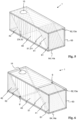
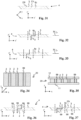
- Fig. 1 is a photography of an optical light guide element 1 of a first type (type I);
- Fig. 2 a schematical perspective illustration of an optical light guide element of a first type (type I). Since the optical light guide elements 1 of Figs. 1 and 2 are, to a large extent, identical (they differ mainly in some dimensions), they are described together, in the following.
- the optical light guide element 1 includes a prism 40 having two reflective faces 51, 52 embodied, e.g., by two reflective coatings 21r, 23r. Light entering the optical light guide element 1 through lens element 15 is reflected by reflective face 52 along a main direction of the optical light guide element 1 onto reflective face 51 which again redirects the light out of optical light guide element 1, e.g., through another lens element (which would be not visible in Figs. 1, 2 ).
- Optical light guide element 1 includes first and third outer side panels 61, 63 which are aligned parallel to base faces 71, 72 of prism 40, and to which base faces 71, 72 are fixed.
- Optical light guide element 1 further includes second and fourth outer side panels 62, 64, which are sections 13a and 14a, respectively, of a lens wafer (cf. below).
- Optical light guide element 1 has, within a cuboid described by the outer side panels 61, 62, 63, 64, two cavities 9, 9'.
- Figs. 3 and 4 illustrate an optical light guide element 1 of a second type (type II). Since many features of the illustrated type II optical light guide element 1 of Figs. 3, 4 are identical with features of the optical light guide element 1 of Figs. 1, 2 , mainly the differences will be explained in the following.
- the optical light guide element 1 includes two prisms 41, 42 which are at a distance. Between prisms 41, 42, there is a cavity 9". Cavity 9" can be enclosed, in particular hermetically enclosed, by outer side panels 61, 62, 63, 63 and prisms 41, 42, as it is the case in the embodiment of Figs. 3, 4 .
- Prism 41 has base faces 71, 72, and prism 42 has base face 73 and another base face not visible in Figs. 3, 4 .
- Each of the base faces is aligned parallel to and is fixed to one of outer side panels 61, 62.
- Light entering optical light guide element 1 through lens element 15 is reflected by first and second reflective faces 51, 52 and propagates between first and second reflective faces 51, 52 inside cavity 9" along the main direction.
- Fig. 5 is a schematical perspective illustration of an optical light guide element 1 of the first type (type I), which is manufactured using further bars (cf. below).
- optical light guide element 1 includes three prisms 40, 41, 42 which roughly correspond to prisms 40, 41, 42 of Figs. 1 through 4 .
- prism 40 can be adjacent to both, prism 41 and prism 42.
- optical light guide element 1 comprises no cavity.
- first and second reflective faces 51, 52 are included in prism 40.
- a reflective coating of one of the other prisms 41, 42 can be dispensed with.
- the optical light guide element 1 is of type I.
- reflective face 51 is realized by prism 41, e.g., by a reflective coating 21r
- reflective face 52 is realized by prism 42, e.g., by a reflective coating 23r.
- the optical light guide element 1 is of type III, because light propagating inside optical light guide element 1 along the main direction does not propagate through a prism bearing the reflective faces (which would be obtained from an initial bar, cf. below).
- optical light guide element 1 could be a type I optical light guide element.
- the base faces of the prisms are, also in case of Fig. 3 , fixed at the inner side of outer side panels 61 and 63, respectively.
- Fig. 6 is a schematical perspective illustration of an optical light guide element 1 of a second type (type II) using total internal reflection (TIR), and manufactured using further bars (cf. below).
- TIR total internal reflection
- optical light guide element 1 includes three prisms 40, 41, 42 which roughly correspond to prisms 40, 41, 42 of Figs. 1 through 5 .
- prism 40 is free of a reflective coating at reflective faces 51, 52.
- the transparent material from which prism 40 is made has a relatively high index of refraction, such that light entering optical light guide element 1 through lens 15 will be reflected towards reflective face 52 by reflective face 51 by TIR.
- the index of refraction of prism 40 can be 1.5 or higher.
- Prisms 41, 42 can protect reflective faces 51, 52 from dirt and damage.
- prisms 41, 42 can be dispensed with.
- optical light guide elements such as optical light guide elements 1 of one or more of Figs. 1 through 6 .
- small coordinate systems are symbolized for explaining the orientation of the illustrated parts.
- x, y, z designate coordinates related to the initial bars
- x', y', z' designate coordinates related to prism bars.
- the manufacturing can be accomplished on wafer level, thus making possible to manufacture high numbers of high precision parts within a relatively small period of time and/or by means of a relatively low number of processing steps.
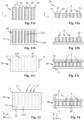
- Figs. 7a-7c are schematical illustrations in a top view of a manufacture of initial bars 2.
- Figs. 8a-8c are schematical illustrations in a cross-sectional view of the manufacture of initial bars 2.
- Figs. 7a, 8a illustrate a plate 6 having an upper face 6a and a lower face 6b, wherein a first reflective coating 21r is present at face 6a, and a second reflective coating 23r is present at face 6b. Between coatings 21r, 23r, an optically transparent material 6c can be present.
- reflective coatings such as coatings 21r, 23r, can, in some instances, be dispensed with.
- Plate 6 is, in some instances further below, also referred to as "P/C wafer".
- Figs. 7b, 8b separation lines are indicated by dashed lines, which are also symbolized in the coordinate systems. By separating plate 6 along these lines, a plurality of initial bars 2 is obtained, as illustrated in Figs. 7c, 8c .
- Each initial bar 2 has a first bar end 28 and a second bar end 29 and four side faces 21, 22, 23, 24, wherein reflective coating 21r is at side face 21, and reflective coating 23r is at side face 23.
- the initial bars 2 In order to produce a bar arrangement 20 (cf., e.g., Figs. 11a, 12a ), the initial bars 2 have to be positioned suitably. Therein, reflective faces of the initial bars 2 face each other. I.e. with respect to the mutual orientation the initial bars have during separation of plate 6 (cf. Figs. 7c, 8c ), each initial bar is rotated by 90° about the y axis corresponding to an initial-bar direction D, cf. Fig. 7c .
- One way of positioning the initial bars 2 is to use a jig 8 as illustrated in Figs. 9a-9c .
- Figs. 9a-9c are schematical illustrations in a cross-sectional view of a positioning of initial bars 2 using a jig 8.
- Jig 8 has a plurality of protrusions 81 on which an initial bar 2 can be positioned each. After attaching initial bars 2 to protrusions 81, spacers 8a are inserted between the initial bars 2 (cf. Fig. 9b ). The spacers 8a can also be considered shims.
- a suitable, e.g., equidistant, spacing of the initial bars 2 is achieved, cf. Fig. 9c .
- jigs may, alternatively, be used, e.g., jig 8' as illustrated in Figs. 10a, 10b .
- Figs. 10a-10b are schematical illustrations in a cross-sectional view of a positioning of initial bars 2 using another jig 8'.
- Jig 8' has grooves 8b into which initial bars 2 can be inserted, thus ensuring a precise mutual alignment of the initial bars 2.
- a jig is used for the positioning only and will be removed later.
- Figs. 11a-11c are schematical illustrations in a top view of a manufacture of a bar arrangement 20, e.g., based on bars positioned as described above.
- Figs. 12a-12c are schematical illustrations in a cross-sectional view of the manufacture of a bar arrangement illustrated in Figs. 11a-11c .
- Figs. 11a, 12a show the bars positioned as required for the desired bar arrangement.
- a jig possibly used for the positioning of the initial bars 2 is not illustrated in Figs. 11a, 12a .
- the initial bars 2 can be fixed relative to each other by attaching one or two substrates to the bar arrangement 20. After attachment to a first substrate, a jig, if applied before, can be removed from the bar arrangement. However, the positioned initial bars as illustrated, e.g., in Figs. 11a, 12a can represent a bar arrangement, too.
- Figs. 11b, 12b illustrate attaching a first substrate 11 to bar arrangement 20.
- Figs. 11c, 12c illustrate attaching a second substrate 12 to bar arrangement 20.
- the initial bars 2 are sandwiched between first and second substrates 11, 12.
- a wafer stack is obtained in which the initial bars 2 are mutually positioned with high precision.
- the obtained wafer stack of Figs. 11c, 12c is separated into bars referred to as prism bars.
- cut lines C of the separation are at an angle with the initial-bar lines D, e.g., at an angle of 45°, as illustrated below.
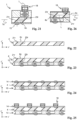
- Fig. 13 is a schematical illustration in a top view of a manufacture of prism bars 4 from the bar arrangement 20 of Figs. 11c, 12c; and Fig. 14 is a schematical illustration in a cross-sectional view of the manufacture of prism bars 4 illustrated in Fig. 13 .
- Fig. 15 is a schematical cross-sectional view of a prism bar 4 as obtained according to Figs. 13, 14 ; and Fig. 16 is a schematical illustration in a cross-sectional view of the prism bar of Fig. 15 . Note the coordinate systems.
- Fig. 15 is basically a detail of Fig. 13 .
- x' is a coordinate along the extension of the prism bar 4 - which runs somewhere (depending on the cutting angle) between the x and y coordinates of the initial bar coordinate system. It corresponds, in the produced optical light guide element to the main direction M of the optical light guide element.
- z' is a height coordinate of the prism bar 4 - which corresponds to the opposite direction of the y coordinate.
- Fig. 17 is a schematical cross-sectional view of a prism bar 4, illustrated in a way slightly different from Fig. 15 . Reflective coatings are symbolized by thick lines.
- Fig. 18 is a schematical illustration in a cross-sectional view of an attaching of the prism bar 4 of Fig. 17 to a lens wafer 13 for manufacturing a type I optical light guide element.
- Lens wafer 13 - which may also be considered a "further substrate” - includes a plurality of lens elements 15. It is possible to position a plurality of prism bars 4 on such a lens wafer 13, e.g., using pick-and-place.
- Fig. 19 is a schematical cross-sectional view of the prism bar of Fig. 17 sandwiched between the lens wafer illustrated in Fig. 18 and another lens wafer 14 (which may also be considered a "further substrate").
- Fig. 20 is a schematical cross-sectional view of the wafer stack of Fig, 19 , with diffractive optical elements 18 attached, e.g., by pick-and-place on wafer level.
- the dashed lines indicate dicing lines, for a next step in which the wafer stack is singulated into parts.
- Fig. 21 is a schematical cross-sectional view of an optical light guide element 1 of type I obtained by separating the wafer stack of Fig. 20 in parts as indicated in Fig. 20 .
- a light path into, through and out of the optical light guide element 1 is illustrated by the dotted line designated L. From this, it is readily undesrstood how the properties of initial bars 2 and prism bars 4 and their constituents translate into properties of the optical light guide element 1.
- Figs. 22 to 25 illustrate, in the same way as Figs. 17 to 20 do, the manufacture of a wafer stack with prism bars 4 and two further wafers 13, 14 such as the illustrated lens wafers 13, 14.
- Fig. 26 is a schematical cross-sectional view of an optical light guide element of type II obtained by separating the wafer stack of Fig. 25 into parts. A light path into, through and out of the optical light guide element 1 is illustrated by the dotted line designated L. From this, it is clear how the properties of initial bars 2 and prism bars 4 and their constituents translate into properties of the optical light guide element 1.
- the initial bars 2 can, in some embodiments, be congeneric, as illustrated in the examples above.
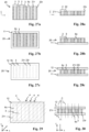
- Figs. 27a-27c are schematical illustrations in a top view of a manufacture of a bar arrangement 20 comprising initial bars 2 and further bars 3.
- Figs. 28a-28c are schematical illustrations in a cross-sectional view of the manufacture of a bar arrangement illustrated in Figs. 27a-27c .
- Further bars 3 can be manufactured in the same way as initial bars 2 are manufactured. They may be obtained by separating a plate, referred to as further plate, into bars.
- Such a further plate can, e.g., be provided with a reflective coating on one of its large faces or with reflective coatings on both of its large faces. But in some embodiments, the further plate does not have a reflective coating.
- Fig. 29 is a schematical illustration in a top view of a manufacture of a prism bar 4 from the bar arrangement of Figs. 27c, 28c; and Fig. 30 is a schematical illustration in a cross-sectional view of the manufacture of a prism bar illustrated in Fig. 29 .
- Fig. 31 is a schematical cross-sectional view of a prism bar 4 as obtained according to Figs. 29, 30 .
- Fig. 32 is a schematical cross-sectional illustration of the prism bar 4 of Fig. 31 , with separation lines illustrated for producing type I optical light guide elements with further bars 3 as filler bars.
- the light path is referenced L.
- Fig. 33 is a schematical cross-sectional illustration of the prism bar 4 of Fig. 31 , with separation lines illustrated for producing type I optical light guide elements with initial bars 2 as filler bars.
- Fig. 34 is a schematical illustration in a top view of a bar arrangement 20 comprising further bars 3 and, at a distance thereto, initial bars 2 which are not coated.
- Fig. 35 is a schematical cross-sectional illustration of the bar arrangement 20 of Fig. 35 sandwiched between two substrates 11, 12. The space between neighboring initial bars 2 and further bars 3 is referenced 99.
- Fig. 36 is a schematical cross-sectional illustration of a prism bar 4 obtained from the bar arrangement of Fig. 35 , with separation lines illustrated for producing type I optical light guide elements with reflectivity at reflective faces by total internal reflection and with further bars 3 as filler bars.
- Fig. 37 is a schematical cross-sectional illustration of a prism bar 4 obtained from a bar arrangement with filler bars 3 at a distance to the initial bars 2 (spaces referenced 99), with separation lines illustrated for producing type III optical light guide elements with initial bars 2 as filler bars.
- Fig. 38 is a schematical cross-sectional view of an optical light guide element 1 of type II including in the cavity 9" an opto-electronic component 90 at side panel 64.
- Side panel 64 is, in part, made of a non-transparent dielectric material.
- Side panel 64 can be, at least in part, a PCB.
- Opto-electronic component 90 is attached to contact pads which are in electrical contact to further contact pads 99 outside cavity 9" by vias 95.
- optical light guide element 1 can be supplied with power and/or be controlled from outside optical light guide element 1.
- optoelectronic component 90 is a light emitter. This way, light produced by optical light guide element 1 (more specifically: by optoelectronic component 90) can propagate along a path similar to (e.g., parallel to) the path of light guided through optical device 1.
- a transparent region 62a is provided to which lens element 15 is attached.
- Panel 64 comprises a transparent region, too, for letting light pass through the otherwise non-transparent panel.
- the optical light guide element 1 can be produced when a printed circuit board is combined with the prism bars, i.e. the printed circuit board (with transparent regions) can be used as a further substrate which replaces or is a lens wafer.
- the further substrates to be used can be printed circuit boards to which opto-electronic components are attached. Accordingly, printed circuit board assemblies can be used as the further substrates.
- Fig. 39 is a schematical cross-sectional view of an optical light guide element 1 of type II including in the cavity 9" an opto-electronic component 90 at prism 42.
- This can be understood as an example for the possibility to produce a superposition of diffuse light (diffuse light produced by optical device 1, more specifically by opto-electronic component 90) and directed light (guided through optical light guide element 1).
- Fig. 39 also illustrates that more than one passive optical component may be included in optical device 1.
- one (15) may be present at a panel (62) through which light exits optical light guide element 1, and another one (15') may be present at panel 64, attached to transparent region 64a through which light enters optical light guide element 1.
- the optical light guide element 1 can be produced when printed circuit boards are used as the initial bars.
- the plates 6 used to produce the initial bars 2 can be printed circuit boards, and opto-electronic components can be placed thereon.
- printed circuit board assemblies can be used as the plates 6.
- initial bars 2 which are reflective only at one side (but not at the opposite side). They can be positioned, e.g., parallel to each other, to produce a bar arrangement, optionally with further bars 3 between the initial bars, wherein the further bars 3 can optionally have no reflective face, one reflective face, or two (oppositely arranged) reflective faces. Spaces 99 between neighboring bars can optionally be provided.
- a special adhesive may be used that is comprised of typical adhesive material and plastic or glass balls/spheres of a particular diameter.
- the spheres precisely define the ultimate thickness of the adhesive layer.
- the various methods and embodiments described may, in some instances, permit the manufacture of light pipes (optical light guide elements) with a very low z height. Additionally, in some instances, very high precision alignment of and distancing between parts (constituents) of the light pipe and/or very high precision alignment of the light pipe and distancing between the light pipe and further items may be achievable.
- the described processes can employ smooth (e.g., polished) material (e.g., glass or other transparent material; or - in particular for type II light pipes, cf. above - also non-transparent material), which may be coated with a highly reflective coating.
- smooth material we mean in the present context material having a planar surface, typically at least from micron scale to millimeter scale (the surface having a low roughness), e.g., like an ordinary mirror does.
- the provision of such material may make possible to overcome various technical challenges.
- the smooth material can be of importance for the light pipes.
- the smooth (e.g., polished and coated) sides effect that the entire smooth material can have a very well defined thickness. This thickness translates into a very well-defined optical path.
- the smooth material is transparent (e.g., polished glass or a polished transparent polymer - e.g., having an index of refraction enabling total internal reflection), and in some other cases, the smooth material is a non-transparent (and possibly also non-reflective) material such as PCB material (e.g., fiber-reinforced epoxy), and in still some other cases, the smooth material is a reflective (in particular highly reflective) non-transparent material such as a metal, e.g., polished aluminium.
- PCB material e.g., fiber-reinforced epoxy
- the smooth material e.g., polished glass mentioned above provides a well defined space/optical path 1.) directly (as in Fig. 1 , type I), where the smooth material defines a prism, or 2.) indirectly (as in Fig. 3 , type II), where an intervening jig with smooth sides is used in conjunction with two smooth material wafers to provide a well-defined optical path (the jig is only temporarily placed between the two prisms, then removed during processing).
Applications Claiming Priority (4)
| Application Number | Priority Date | Filing Date | Title |
|---|---|---|---|
| US201462079080P | 2014-11-13 | 2014-11-13 | |
| US201562160224P | 2015-05-12 | 2015-05-12 | |
| US201562211436P | 2015-08-28 | 2015-08-28 | |
| PCT/SG2015/050443 WO2016076797A1 (en) | 2014-11-13 | 2015-11-11 | Manufacture of optical light guides |
Publications (3)
| Publication Number | Publication Date |
|---|---|
| EP3218746A1 EP3218746A1 (en) | 2017-09-20 |
| EP3218746A4 EP3218746A4 (en) | 2018-11-07 |
| EP3218746B1 true EP3218746B1 (en) | 2023-09-27 |
Family
ID=55954738
Family Applications (1)
| Application Number | Title | Priority Date | Filing Date |
|---|---|---|---|
| EP15858304.7A Active EP3218746B1 (en) | 2014-11-13 | 2015-11-11 | Manufacture of optical light guides |
Country Status (8)
| Country | Link |
|---|---|
| US (2) | US20170336543A1 (ko) |
| EP (1) | EP3218746B1 (ko) |
| JP (1) | JP6866290B2 (ko) |
| KR (1) | KR102603829B1 (ko) |
| CN (1) | CN107003475B (ko) |
| SG (1) | SG11201703102VA (ko) |
| TW (1) | TWI708971B (ko) |
| WO (1) | WO2016076797A1 (ko) |
Families Citing this family (9)
| Publication number | Priority date | Publication date | Assignee | Title |
|---|---|---|---|---|
| US10551602B2 (en) | 2015-08-28 | 2020-02-04 | Ams Sensors Singapore Pte. Ltd. | Wafer-level optical device having light guide properties |
| US10302863B2 (en) | 2016-05-06 | 2019-05-28 | Ams Sensors Singapore Pte. Ltd. | Methods of attaching surfaces together by adhesives, and devices including surfaces attached together by adhesives |
| TWI743188B (zh) * | 2016-09-20 | 2021-10-21 | 新加坡商新加坡恒立私人有限公司 | 光學裝置、具有此裝置之合成光學裝置及製造此裝置之方法 |
| TWI753103B (zh) * | 2017-02-10 | 2022-01-21 | 新加坡商海特根微光學公司 | 光導及光導之製造 |
| IL251645B (en) * | 2017-04-06 | 2018-08-30 | Lumus Ltd | Waveguide and method of production |
| US20190094069A1 (en) * | 2017-09-27 | 2019-03-28 | Apple Inc. | Electronic Devices Having Infrared Blocking Light Guides |
| AU2021279462B2 (en) * | 2020-05-24 | 2023-06-08 | Lumus Ltd. | Method of fabrication of compound light-guide optical elements |
| US11762174B2 (en) | 2020-09-24 | 2023-09-19 | Apple Inc. | Optical system including lenses and prism for telephoto cameras |
| US20220091398A1 (en) * | 2020-09-24 | 2022-03-24 | Apple Inc. | Telephoto Camera with a Stationary Optics Assembly |
Family Cites Families (16)
| Publication number | Priority date | Publication date | Assignee | Title |
|---|---|---|---|---|
| US6404550B1 (en) * | 1996-07-25 | 2002-06-11 | Seiko Epson Corporation | Optical element suitable for projection display apparatus |
| JPH11326749A (ja) * | 1998-05-08 | 1999-11-26 | Asahi Optical Co Ltd | カメラの焦点検出装置 |
| US6400876B1 (en) * | 1998-08-31 | 2002-06-04 | Brookhaven Science Associates | Ultrathin optical panel and a method of making an ultrathin optical panel |
| JP4006855B2 (ja) * | 1998-10-30 | 2007-11-14 | エプソントヨコム株式会社 | 光学デバイスの製造方法 |
| JP3666463B2 (ja) * | 2002-03-13 | 2005-06-29 | 日本電気株式会社 | 光導波路デバイスおよび光導波路デバイスの製造方法 |
| JP2004144678A (ja) * | 2002-10-25 | 2004-05-20 | Arkray Inc | 光学ユニット、光センサ、マルチチャンネル光検出装置及び光学ユニットの製造方法 |
| IL157837A (en) * | 2003-09-10 | 2012-12-31 | Yaakov Amitai | Substrate-guided optical device particularly for three-dimensional displays |
| JP2005202060A (ja) * | 2004-01-14 | 2005-07-28 | Olympus Corp | 観察光学系 |
| JP4821614B2 (ja) * | 2004-12-16 | 2011-11-24 | 東レ株式会社 | 偏光板、その製造方法およびそれを用いた液晶表示装置 |
| JP4925979B2 (ja) * | 2007-09-05 | 2012-05-09 | 新光電気工業株式会社 | 光導波路の形成方法、光導波路、および光電混載回路 |
| US20090126792A1 (en) * | 2007-11-16 | 2009-05-21 | Qualcomm Incorporated | Thin film solar concentrator/collector |
| JP5550535B2 (ja) * | 2010-11-26 | 2014-07-16 | 新光電気工業株式会社 | 光導波路装置及びその製造方法 |
| WO2012071674A1 (en) * | 2010-11-30 | 2012-06-07 | Ville Kettunen | Optical light guide element for an electronic device |
| CN103959465B (zh) * | 2011-10-06 | 2019-06-07 | 新加坡恒立私人有限公司 | 用于物体的晶片级制造的方法以及相应的中间产品 |
| JP6114049B2 (ja) * | 2013-02-04 | 2017-04-12 | Hoya株式会社 | 撮像装置 |
| TWI743188B (zh) * | 2016-09-20 | 2021-10-21 | 新加坡商新加坡恒立私人有限公司 | 光學裝置、具有此裝置之合成光學裝置及製造此裝置之方法 |
-
2015
- 2015-11-11 KR KR1020177013040A patent/KR102603829B1/ko active IP Right Grant
- 2015-11-11 JP JP2017525955A patent/JP6866290B2/ja active Active
- 2015-11-11 SG SG11201703102VA patent/SG11201703102VA/en unknown
- 2015-11-11 CN CN201580059466.1A patent/CN107003475B/zh active Active
- 2015-11-11 EP EP15858304.7A patent/EP3218746B1/en active Active
- 2015-11-11 WO PCT/SG2015/050443 patent/WO2016076797A1/en active Application Filing
- 2015-11-11 US US15/522,423 patent/US20170336543A1/en not_active Abandoned
- 2015-11-12 TW TW104137341A patent/TWI708971B/zh active
-
2021
- 2021-05-12 US US17/318,345 patent/US20210333445A1/en active Pending
Also Published As
| Publication number | Publication date |
|---|---|
| KR20170081654A (ko) | 2017-07-12 |
| TW201629553A (zh) | 2016-08-16 |
| KR102603829B1 (ko) | 2023-11-17 |
| TWI708971B (zh) | 2020-11-01 |
| JP2018500589A (ja) | 2018-01-11 |
| EP3218746A4 (en) | 2018-11-07 |
| CN107003475A (zh) | 2017-08-01 |
| JP6866290B2 (ja) | 2021-04-28 |
| EP3218746A1 (en) | 2017-09-20 |
| US20170336543A1 (en) | 2017-11-23 |
| WO2016076797A1 (en) | 2016-05-19 |
| CN107003475B (zh) | 2020-10-27 |
| SG11201703102VA (en) | 2017-05-30 |
| US20210333445A1 (en) | 2021-10-28 |
Similar Documents
| Publication | Publication Date | Title |
|---|---|---|
| EP3218746B1 (en) | Manufacture of optical light guides | |
| US7590315B2 (en) | Optical waveguide and optical module using the same | |
| KR101194452B1 (ko) | 광전자 기기 상의 마이크로 광학 기기 | |
| JP5159897B2 (ja) | 回路基板に実装される光導波路のための光タップ | |
| JP5109982B2 (ja) | ミラー付き光伝送体の製造方法 | |
| JP2017167533A (ja) | 受動光学構成要素の製造方法および受動光学構成要素を備えるデバイス | |
| TW201533486A (zh) | 光傳送模組及光傳送模組之製造方法 | |
| JPH04286191A (ja) | 回路板を相互接続する光学的背面(バックプレーン) | |
| US7747115B2 (en) | Optical waveguide device and light outputting module | |
| US20100316343A1 (en) | Optical waveguide and method of manufacturing the same, and optical waveguide mounted board | |
| US8737794B2 (en) | Two-layer optical waveguide and method of manufacturing the same | |
| JP2015129795A (ja) | 光ファイバコネクタ及び光通信モジュール | |
| SE525405C2 (sv) | Speglar för polymera vägledare, förfarande för deras framställning, samt optisk vågledaranordning | |
| NL2013524A (en) | An optical light guide element and a method for manufacturing. | |
| US6907178B2 (en) | Optoelectronic assembly with embedded optical and electrical components | |
| JP4609311B2 (ja) | 光送受信器 | |
| JP4469289B2 (ja) | 光路変換ミラーの製法 | |
| JP4607063B2 (ja) | 光路変換コネクタの製造方法 | |
| JP4290065B2 (ja) | 光モジュールおよびその製造方法 | |
| JP2009103860A (ja) | 光導波路および光導波路製造方法 | |
| JP2016018147A (ja) | ミラー付き光回路及びミラー付き光回路の製造方法 | |
| JP2009098432A (ja) | 貼り合わせ多チャンネル光路変換素子とその作製方法 | |
| JP2009223340A (ja) | 光学部品、およびそれに用いられる光路変換デバイス | |
| JP2010224246A (ja) | 光基板の製造方法 | |
| JP2009223339A (ja) | 光路変換コネクタ、およびその製造方法、並びに光路変換コネクタを具備する回路基板 |
Legal Events
| Date | Code | Title | Description |
|---|---|---|---|
| STAA | Information on the status of an ep patent application or granted ep patent |
Free format text: STATUS: THE INTERNATIONAL PUBLICATION HAS BEEN MADE |
|
| PUAI | Public reference made under article 153(3) epc to a published international application that has entered the european phase |
Free format text: ORIGINAL CODE: 0009012 |
|
| STAA | Information on the status of an ep patent application or granted ep patent |
Free format text: STATUS: REQUEST FOR EXAMINATION WAS MADE |
|
| 17P | Request for examination filed |
Effective date: 20170331 |
|
| AK | Designated contracting states |
Kind code of ref document: A1 Designated state(s): AL AT BE BG CH CY CZ DE DK EE ES FI FR GB GR HR HU IE IS IT LI LT LU LV MC MK MT NL NO PL PT RO RS SE SI SK SM TR |
|
| AX | Request for extension of the european patent |
Extension state: BA ME |
|
| DAV | Request for validation of the european patent (deleted) | ||
| DAX | Request for extension of the european patent (deleted) | ||
| RIC1 | Information provided on ipc code assigned before grant |
Ipc: G02B 13/00 20060101ALI20180702BHEP Ipc: G02B 6/10 20060101AFI20180702BHEP Ipc: G02B 17/00 20060101ALI20180702BHEP |
|
| A4 | Supplementary search report drawn up and despatched |
Effective date: 20181010 |
|
| RIC1 | Information provided on ipc code assigned before grant |
Ipc: G02B 6/10 20060101AFI20181004BHEP Ipc: G02B 17/00 20060101ALI20181004BHEP Ipc: G02B 13/00 20060101ALI20181004BHEP |
|
| STAA | Information on the status of an ep patent application or granted ep patent |
Free format text: STATUS: EXAMINATION IS IN PROGRESS |
|
| 17Q | First examination report despatched |
Effective date: 20210218 |
|
| STAA | Information on the status of an ep patent application or granted ep patent |
Free format text: STATUS: EXAMINATION IS IN PROGRESS |
|
| GRAP | Despatch of communication of intention to grant a patent |
Free format text: ORIGINAL CODE: EPIDOSNIGR1 |
|
| STAA | Information on the status of an ep patent application or granted ep patent |
Free format text: STATUS: GRANT OF PATENT IS INTENDED |
|
| INTG | Intention to grant announced |
Effective date: 20230414 |
|
| INTG | Intention to grant announced |
Effective date: 20230414 |
|
| P01 | Opt-out of the competence of the unified patent court (upc) registered |
Effective date: 20230613 |
|
| GRAS | Grant fee paid |
Free format text: ORIGINAL CODE: EPIDOSNIGR3 |
|
| GRAA | (expected) grant |
Free format text: ORIGINAL CODE: 0009210 |
|
| STAA | Information on the status of an ep patent application or granted ep patent |
Free format text: STATUS: THE PATENT HAS BEEN GRANTED |
|
| AK | Designated contracting states |
Kind code of ref document: B1 Designated state(s): AL AT BE BG CH CY CZ DE DK EE ES FI FR GB GR HR HU IE IS IT LI LT LU LV MC MK MT NL NO PL PT RO RS SE SI SK SM TR |
|
| REG | Reference to a national code |
Ref country code: GB Ref legal event code: FG4D |
|
| REG | Reference to a national code |
Ref country code: CH Ref legal event code: EP |
|
| REG | Reference to a national code |
Ref country code: DE Ref legal event code: R096 Ref document number: 602015085874 Country of ref document: DE |
|
| REG | Reference to a national code |
Ref country code: IE Ref legal event code: FG4D |
|
| REG | Reference to a national code |
Ref country code: LT Ref legal event code: MG9D |
|
| PG25 | Lapsed in a contracting state [announced via postgrant information from national office to epo] |
Ref country code: GR Free format text: LAPSE BECAUSE OF FAILURE TO SUBMIT A TRANSLATION OF THE DESCRIPTION OR TO PAY THE FEE WITHIN THE PRESCRIBED TIME-LIMIT Effective date: 20231228 |
|
| PG25 | Lapsed in a contracting state [announced via postgrant information from national office to epo] |
Ref country code: SE Free format text: LAPSE BECAUSE OF FAILURE TO SUBMIT A TRANSLATION OF THE DESCRIPTION OR TO PAY THE FEE WITHIN THE PRESCRIBED TIME-LIMIT Effective date: 20230927 Ref country code: RS Free format text: LAPSE BECAUSE OF FAILURE TO SUBMIT A TRANSLATION OF THE DESCRIPTION OR TO PAY THE FEE WITHIN THE PRESCRIBED TIME-LIMIT Effective date: 20230927 Ref country code: NO Free format text: LAPSE BECAUSE OF FAILURE TO SUBMIT A TRANSLATION OF THE DESCRIPTION OR TO PAY THE FEE WITHIN THE PRESCRIBED TIME-LIMIT Effective date: 20231227 Ref country code: LV Free format text: LAPSE BECAUSE OF FAILURE TO SUBMIT A TRANSLATION OF THE DESCRIPTION OR TO PAY THE FEE WITHIN THE PRESCRIBED TIME-LIMIT Effective date: 20230927 Ref country code: LT Free format text: LAPSE BECAUSE OF FAILURE TO SUBMIT A TRANSLATION OF THE DESCRIPTION OR TO PAY THE FEE WITHIN THE PRESCRIBED TIME-LIMIT Effective date: 20230927 Ref country code: HR Free format text: LAPSE BECAUSE OF FAILURE TO SUBMIT A TRANSLATION OF THE DESCRIPTION OR TO PAY THE FEE WITHIN THE PRESCRIBED TIME-LIMIT Effective date: 20230927 Ref country code: GR Free format text: LAPSE BECAUSE OF FAILURE TO SUBMIT A TRANSLATION OF THE DESCRIPTION OR TO PAY THE FEE WITHIN THE PRESCRIBED TIME-LIMIT Effective date: 20231228 Ref country code: FI Free format text: LAPSE BECAUSE OF FAILURE TO SUBMIT A TRANSLATION OF THE DESCRIPTION OR TO PAY THE FEE WITHIN THE PRESCRIBED TIME-LIMIT Effective date: 20230927 |
|
| PGFP | Annual fee paid to national office [announced via postgrant information from national office to epo] |
Ref country code: DE Payment date: 20231121 Year of fee payment: 9 |
|
| REG | Reference to a national code |
Ref country code: NL Ref legal event code: MP Effective date: 20230927 |
|
| REG | Reference to a national code |
Ref country code: AT Ref legal event code: MK05 Ref document number: 1615963 Country of ref document: AT Kind code of ref document: T Effective date: 20230927 |
|
| PG25 | Lapsed in a contracting state [announced via postgrant information from national office to epo] |
Ref country code: NL Free format text: LAPSE BECAUSE OF FAILURE TO SUBMIT A TRANSLATION OF THE DESCRIPTION OR TO PAY THE FEE WITHIN THE PRESCRIBED TIME-LIMIT Effective date: 20230927 |
|
| PG25 | Lapsed in a contracting state [announced via postgrant information from national office to epo] |
Ref country code: IS Free format text: LAPSE BECAUSE OF FAILURE TO SUBMIT A TRANSLATION OF THE DESCRIPTION OR TO PAY THE FEE WITHIN THE PRESCRIBED TIME-LIMIT Effective date: 20240127 |
|
| PG25 | Lapsed in a contracting state [announced via postgrant information from national office to epo] |
Ref country code: AT Free format text: LAPSE BECAUSE OF FAILURE TO SUBMIT A TRANSLATION OF THE DESCRIPTION OR TO PAY THE FEE WITHIN THE PRESCRIBED TIME-LIMIT Effective date: 20230927 |
|
| PG25 | Lapsed in a contracting state [announced via postgrant information from national office to epo] |
Ref country code: ES Free format text: LAPSE BECAUSE OF FAILURE TO SUBMIT A TRANSLATION OF THE DESCRIPTION OR TO PAY THE FEE WITHIN THE PRESCRIBED TIME-LIMIT Effective date: 20230927 |
|
| PG25 | Lapsed in a contracting state [announced via postgrant information from national office to epo] |
Ref country code: SM Free format text: LAPSE BECAUSE OF FAILURE TO SUBMIT A TRANSLATION OF THE DESCRIPTION OR TO PAY THE FEE WITHIN THE PRESCRIBED TIME-LIMIT Effective date: 20230927 Ref country code: RO Free format text: LAPSE BECAUSE OF FAILURE TO SUBMIT A TRANSLATION OF THE DESCRIPTION OR TO PAY THE FEE WITHIN THE PRESCRIBED TIME-LIMIT Effective date: 20230927 Ref country code: IS Free format text: LAPSE BECAUSE OF FAILURE TO SUBMIT A TRANSLATION OF THE DESCRIPTION OR TO PAY THE FEE WITHIN THE PRESCRIBED TIME-LIMIT Effective date: 20240127 Ref country code: ES Free format text: LAPSE BECAUSE OF FAILURE TO SUBMIT A TRANSLATION OF THE DESCRIPTION OR TO PAY THE FEE WITHIN THE PRESCRIBED TIME-LIMIT Effective date: 20230927 Ref country code: EE Free format text: LAPSE BECAUSE OF FAILURE TO SUBMIT A TRANSLATION OF THE DESCRIPTION OR TO PAY THE FEE WITHIN THE PRESCRIBED TIME-LIMIT Effective date: 20230927 Ref country code: CZ Free format text: LAPSE BECAUSE OF FAILURE TO SUBMIT A TRANSLATION OF THE DESCRIPTION OR TO PAY THE FEE WITHIN THE PRESCRIBED TIME-LIMIT Effective date: 20230927 Ref country code: AT Free format text: LAPSE BECAUSE OF FAILURE TO SUBMIT A TRANSLATION OF THE DESCRIPTION OR TO PAY THE FEE WITHIN THE PRESCRIBED TIME-LIMIT Effective date: 20230927 Ref country code: PT Free format text: LAPSE BECAUSE OF FAILURE TO SUBMIT A TRANSLATION OF THE DESCRIPTION OR TO PAY THE FEE WITHIN THE PRESCRIBED TIME-LIMIT Effective date: 20240129 Ref country code: SK Free format text: LAPSE BECAUSE OF FAILURE TO SUBMIT A TRANSLATION OF THE DESCRIPTION OR TO PAY THE FEE WITHIN THE PRESCRIBED TIME-LIMIT Effective date: 20230927 |