EP3214701B1 - Elektrische verbindungsstruktur zur verbindung einer sammelschiene an eine elektrische komponente - Google Patents
Elektrische verbindungsstruktur zur verbindung einer sammelschiene an eine elektrische komponente Download PDFInfo
- Publication number
- EP3214701B1 EP3214701B1 EP17158861.9A EP17158861A EP3214701B1 EP 3214701 B1 EP3214701 B1 EP 3214701B1 EP 17158861 A EP17158861 A EP 17158861A EP 3214701 B1 EP3214701 B1 EP 3214701B1
- Authority
- EP
- European Patent Office
- Prior art keywords
- bar
- tab
- leg
- board
- clamp
- Prior art date
- Legal status (The legal status is an assumption and is not a legal conclusion. Google has not performed a legal analysis and makes no representation as to the accuracy of the status listed.)
- Active
Links
Images


Classifications
-
- H—ELECTRICITY
- H01—ELECTRIC ELEMENTS
- H01R—ELECTRICALLY-CONDUCTIVE CONNECTIONS; STRUCTURAL ASSOCIATIONS OF A PLURALITY OF MUTUALLY-INSULATED ELECTRICAL CONNECTING ELEMENTS; COUPLING DEVICES; CURRENT COLLECTORS
- H01R4/00—Electrically-conductive connections between two or more conductive members in direct contact, i.e. touching one another; Means for effecting or maintaining such contact; Electrically-conductive connections having two or more spaced connecting locations for conductors and using contact members penetrating insulation
- H01R4/28—Clamped connections, spring connections
- H01R4/48—Clamped connections, spring connections utilising a spring, clip, or other resilient member
-
- H—ELECTRICITY
- H05—ELECTRIC TECHNIQUES NOT OTHERWISE PROVIDED FOR
- H05K—PRINTED CIRCUITS; CASINGS OR CONSTRUCTIONAL DETAILS OF ELECTRIC APPARATUS; MANUFACTURE OF ASSEMBLAGES OF ELECTRICAL COMPONENTS
- H05K1/00—Printed circuits
- H05K1/18—Printed circuits structurally associated with non-printed electric components
- H05K1/181—Printed circuits structurally associated with non-printed electric components associated with surface mounted components
-
- H—ELECTRICITY
- H01—ELECTRIC ELEMENTS
- H01R—ELECTRICALLY-CONDUCTIVE CONNECTIONS; STRUCTURAL ASSOCIATIONS OF A PLURALITY OF MUTUALLY-INSULATED ELECTRICAL CONNECTING ELEMENTS; COUPLING DEVICES; CURRENT COLLECTORS
- H01R12/00—Structural associations of a plurality of mutually-insulated electrical connecting elements, specially adapted for printed circuits, e.g. printed circuit boards [PCB], flat or ribbon cables, or like generally planar structures, e.g. terminal strips, terminal blocks; Coupling devices specially adapted for printed circuits, flat or ribbon cables, or like generally planar structures; Terminals specially adapted for contact with, or insertion into, printed circuits, flat or ribbon cables, or like generally planar structures
- H01R12/50—Fixed connections
- H01R12/51—Fixed connections for rigid printed circuits or like structures
- H01R12/55—Fixed connections for rigid printed circuits or like structures characterised by the terminals
- H01R12/57—Fixed connections for rigid printed circuits or like structures characterised by the terminals surface mounting terminals
-
- H—ELECTRICITY
- H01—ELECTRIC ELEMENTS
- H01F—MAGNETS; INDUCTANCES; TRANSFORMERS; SELECTION OF MATERIALS FOR THEIR MAGNETIC PROPERTIES
- H01F27/00—Details of transformers or inductances, in general
- H01F27/06—Mounting, supporting or suspending transformers, reactors or choke coils not being of the signal type
-
- H—ELECTRICITY
- H01—ELECTRIC ELEMENTS
- H01R—ELECTRICALLY-CONDUCTIVE CONNECTIONS; STRUCTURAL ASSOCIATIONS OF A PLURALITY OF MUTUALLY-INSULATED ELECTRICAL CONNECTING ELEMENTS; COUPLING DEVICES; CURRENT COLLECTORS
- H01R11/00—Individual connecting elements providing two or more spaced connecting locations for conductive members which are, or may be, thereby interconnected, e.g. end pieces for wires or cables supported by the wire or cable and having means for facilitating electrical connection to some other wire, terminal, or conductive member, blocks of binding posts
- H01R11/11—End pieces or tapping pieces for wires, supported by the wire and for facilitating electrical connection to some other wire, terminal or conductive member
- H01R11/28—End pieces consisting of a ferrule or sleeve
-
- H—ELECTRICITY
- H01—ELECTRIC ELEMENTS
- H01R—ELECTRICALLY-CONDUCTIVE CONNECTIONS; STRUCTURAL ASSOCIATIONS OF A PLURALITY OF MUTUALLY-INSULATED ELECTRICAL CONNECTING ELEMENTS; COUPLING DEVICES; CURRENT COLLECTORS
- H01R12/00—Structural associations of a plurality of mutually-insulated electrical connecting elements, specially adapted for printed circuits, e.g. printed circuit boards [PCB], flat or ribbon cables, or like generally planar structures, e.g. terminal strips, terminal blocks; Coupling devices specially adapted for printed circuits, flat or ribbon cables, or like generally planar structures; Terminals specially adapted for contact with, or insertion into, printed circuits, flat or ribbon cables, or like generally planar structures
- H01R12/50—Fixed connections
- H01R12/51—Fixed connections for rigid printed circuits or like structures
- H01R12/55—Fixed connections for rigid printed circuits or like structures characterised by the terminals
- H01R12/58—Fixed connections for rigid printed circuits or like structures characterised by the terminals terminals for insertion into holes
-
- H—ELECTRICITY
- H01—ELECTRIC ELEMENTS
- H01R—ELECTRICALLY-CONDUCTIVE CONNECTIONS; STRUCTURAL ASSOCIATIONS OF A PLURALITY OF MUTUALLY-INSULATED ELECTRICAL CONNECTING ELEMENTS; COUPLING DEVICES; CURRENT COLLECTORS
- H01R12/00—Structural associations of a plurality of mutually-insulated electrical connecting elements, specially adapted for printed circuits, e.g. printed circuit boards [PCB], flat or ribbon cables, or like generally planar structures, e.g. terminal strips, terminal blocks; Coupling devices specially adapted for printed circuits, flat or ribbon cables, or like generally planar structures; Terminals specially adapted for contact with, or insertion into, printed circuits, flat or ribbon cables, or like generally planar structures
- H01R12/70—Coupling devices
- H01R12/7088—Arrangements for power supply
-
- H—ELECTRICITY
- H01—ELECTRIC ELEMENTS
- H01R—ELECTRICALLY-CONDUCTIVE CONNECTIONS; STRUCTURAL ASSOCIATIONS OF A PLURALITY OF MUTUALLY-INSULATED ELECTRICAL CONNECTING ELEMENTS; COUPLING DEVICES; CURRENT COLLECTORS
- H01R12/00—Structural associations of a plurality of mutually-insulated electrical connecting elements, specially adapted for printed circuits, e.g. printed circuit boards [PCB], flat or ribbon cables, or like generally planar structures, e.g. terminal strips, terminal blocks; Coupling devices specially adapted for printed circuits, flat or ribbon cables, or like generally planar structures; Terminals specially adapted for contact with, or insertion into, printed circuits, flat or ribbon cables, or like generally planar structures
- H01R12/70—Coupling devices
- H01R12/71—Coupling devices for rigid printing circuits or like structures
- H01R12/75—Coupling devices for rigid printing circuits or like structures connecting to cables except for flat or ribbon cables
-
- H—ELECTRICITY
- H01—ELECTRIC ELEMENTS
- H01R—ELECTRICALLY-CONDUCTIVE CONNECTIONS; STRUCTURAL ASSOCIATIONS OF A PLURALITY OF MUTUALLY-INSULATED ELECTRICAL CONNECTING ELEMENTS; COUPLING DEVICES; CURRENT COLLECTORS
- H01R25/00—Coupling parts adapted for simultaneous co-operation with two or more identical counterparts, e.g. for distributing energy to two or more circuits
- H01R25/16—Rails or bus-bars provided with a plurality of discrete connecting locations for counterparts
- H01R25/161—Details
- H01R25/162—Electrical connections between or with rails or bus-bars
-
- H—ELECTRICITY
- H01—ELECTRIC ELEMENTS
- H01R—ELECTRICALLY-CONDUCTIVE CONNECTIONS; STRUCTURAL ASSOCIATIONS OF A PLURALITY OF MUTUALLY-INSULATED ELECTRICAL CONNECTING ELEMENTS; COUPLING DEVICES; CURRENT COLLECTORS
- H01R25/00—Coupling parts adapted for simultaneous co-operation with two or more identical counterparts, e.g. for distributing energy to two or more circuits
- H01R25/16—Rails or bus-bars provided with a plurality of discrete connecting locations for counterparts
- H01R25/165—Connecting locations formed by surface mounted apparatus
-
- H—ELECTRICITY
- H01—ELECTRIC ELEMENTS
- H01R—ELECTRICALLY-CONDUCTIVE CONNECTIONS; STRUCTURAL ASSOCIATIONS OF A PLURALITY OF MUTUALLY-INSULATED ELECTRICAL CONNECTING ELEMENTS; COUPLING DEVICES; CURRENT COLLECTORS
- H01R4/00—Electrically-conductive connections between two or more conductive members in direct contact, i.e. touching one another; Means for effecting or maintaining such contact; Electrically-conductive connections having two or more spaced connecting locations for conductors and using contact members penetrating insulation
- H01R4/02—Soldered or welded connections
-
- H—ELECTRICITY
- H02—GENERATION; CONVERSION OR DISTRIBUTION OF ELECTRIC POWER
- H02G—INSTALLATION OF ELECTRIC CABLES OR LINES, OR OF COMBINED OPTICAL AND ELECTRIC CABLES OR LINES
- H02G5/00—Installations of bus-bars
- H02G5/02—Open installations
-
- H—ELECTRICITY
- H01—ELECTRIC ELEMENTS
- H01F—MAGNETS; INDUCTANCES; TRANSFORMERS; SELECTION OF MATERIALS FOR THEIR MAGNETIC PROPERTIES
- H01F27/00—Details of transformers or inductances, in general
- H01F27/06—Mounting, supporting or suspending transformers, reactors or choke coils not being of the signal type
- H01F2027/065—Mounting on printed circuit boards
-
- H—ELECTRICITY
- H01—ELECTRIC ELEMENTS
- H01R—ELECTRICALLY-CONDUCTIVE CONNECTIONS; STRUCTURAL ASSOCIATIONS OF A PLURALITY OF MUTUALLY-INSULATED ELECTRICAL CONNECTING ELEMENTS; COUPLING DEVICES; CURRENT COLLECTORS
- H01R2201/00—Connectors or connections adapted for particular applications
- H01R2201/22—Connectors or connections adapted for particular applications for transformers or coils
-
- H—ELECTRICITY
- H05—ELECTRIC TECHNIQUES NOT OTHERWISE PROVIDED FOR
- H05K—PRINTED CIRCUITS; CASINGS OR CONSTRUCTIONAL DETAILS OF ELECTRIC APPARATUS; MANUFACTURE OF ASSEMBLAGES OF ELECTRICAL COMPONENTS
- H05K2201/00—Indexing scheme relating to printed circuits covered by H05K1/00
- H05K2201/10—Details of components or other objects attached to or integrated in a printed circuit board
- H05K2201/10007—Types of components
- H05K2201/1003—Non-printed inductor
-
- H—ELECTRICITY
- H05—ELECTRIC TECHNIQUES NOT OTHERWISE PROVIDED FOR
- H05K—PRINTED CIRCUITS; CASINGS OR CONSTRUCTIONAL DETAILS OF ELECTRIC APPARATUS; MANUFACTURE OF ASSEMBLAGES OF ELECTRICAL COMPONENTS
- H05K2201/00—Indexing scheme relating to printed circuits covered by H05K1/00
- H05K2201/10—Details of components or other objects attached to or integrated in a printed circuit board
- H05K2201/10227—Other objects, e.g. metallic pieces
- H05K2201/10272—Busbars, i.e. thick metal bars mounted on the printed circuit board [PCB] as high-current conductors
Definitions
- the invention relates to a system for the mechanical and electrical connection of an electrical current transmission bar to an electrical component.
- the invention relates more particularly to a connection system for a module of an electrical installation, comprising an electric current transformer mounted on a printed circuit board, which is connected to a connector of the module by conductive bars for the transmission of strong currents.
- a medium voltage current transmission network comprises in particular a protection cell made up of a plurality of modules having different functions such as, for example, Input / Output, Power, Communication or Current / Voltage Acquisition functions. This makes it possible to offer a wide variety of applications for medium voltage networks.
- One of these modules which is the current / voltage acquisition module, consists of an electrical installation comprising, as main components: a current acquisition transformer (CT Current Transformer), a customer connector which makes it possible to connect the primary of the transformer, an analog conversion chain and a connection connector to the motherboard. These components are mounted on a printed circuit board.
- CT Current Transformer current acquisition transformer
- customer connector which makes it possible to connect the primary of the transformer
- analog conversion chain an analog conversion chain
- connection connector to the motherboard.
- the primary circuit of the transformer is crossed by a high intensity current. This implies using conductors with a large section to make this circuit.
- the wiring of the module using conductors in the form of electric wires is carried out manually by an operator, which involves a risk error, as well as a complexity of the routing of the cables influencing the performance of the module, in particular for so-called crosstalk problems.
- Connecting components with busbars involves bending each bar as it is cabled.
- the rigidity of the bars makes their connection to the transformer difficult and technically complex in its practical realization, without systematically guaranteeing a mechanical connection.
- the object of the invention is to provide a system for the mechanical and electrical connection of a conductor bar to any other electrical component, such as the current transformer, which is simple to implement and which ensures reliable mechanical and electrical connections.
- the invention relates to a mechanical and electrical connection system comprising as defined in claim 1.
- the clamp has a lower part which is received in the second orifice with the tab of the component.
- the plate comprises a layer of continuous conductive material formed at the level of the orifices and which covers at least one lower face of the plate, surrounding the openings of the orifices, and which may also cover the upper face of the plate and the walls. orifices.
- part of the layer of conductive material, which covers a lower face of the plate is covered with a brazing material.
- the clamp consists of at least two hooks jointly delimiting a cylindrical housing and are able to move apart when the tab is introduced into said housing.
- each hook has at least one tongue extending parallel to the main axis of the housing, the lower end of each tongue of which is located vertically below a lower face of the plate and protrudes towards the bottom. outside of the hook.
- the conductive bar consists of two half-bars which are distributed on either side of a median vertical longitudinal plane of the bar and which are connected to each other at their edge. upper end by a fold line.
- each half bar has a hook and half of the foot.
- the fold line forms a broken line and comprises a plurality of windows distributed longitudinally along the fold line.
- the conductive bar is produced by folding a blank of conductive material which has been previously cut and stamped.
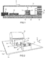
- a module 10 for a protection cell intended to be installed in a medium voltage current transmission line This module 10 is for example a current / voltage acquisition module.
- the module 10 comprises a printed circuit board 12 on which numerous electronic components are mounted.
- the plate 12 extends along a horizontal main plane with the longitudinal direction from front to rear being the direction from right to left with reference to the figure 1 .
- the module 10 here comprises a front connector 14 for mounting and connecting the module 10 in the cell, a current acquisition transformer 16, an analog conversion chain 18 and a rear connector 20 for connecting the module 10 to a card. mother of the cell.
- the transformer 16 comprises a primary circuit 22 which is connected to the front connector 14 and a secondary circuit 24 connected to the analog conversion chain 18.
- the current which circulates between the front connector 14 and the primary circuit 22 comes directly from the secondary circuit d another current transformer (not shown) installed in the cell and is carried by conductors 26.
- the various components of the module 10 are shown here as being mounted on the same upper face 12s of the plate, its lower face 12i being empty.
- module 10 can include other components mounted on this lower face 12i of the plate 12, in addition to those mounted on its upper face 12s.
- each conductor 26 consists of a bar whose section is of rectangular main shape, the great length of its section being vertical.
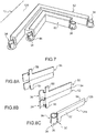
- each bar 26 extends longitudinally. It will be understood that the invention is not limited to this configuration of the bars 26, which can be bent at different angles, as shown for example on figure 7 .
- Each end of a bar 26 is connected to a component of the module 10, that is to say here a first longitudinal end 26a of the bar 26 is connected to the transformer 16, the second end 26b of the bar 26 is connected to the front connector 14.
- first end 26a of the bar 26 is oriented longitudinally. It will be understood that this orientation is not limiting and that one end of a bar 26 can be oriented differently without departing from the scope of the invention, while remaining parallel to the main plane of the plate 12.
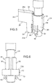
- connection lug 28 for its connection with the bar 26, the electrical component, which here is the transformer 16, has a connection lug 28.
- This tab 28 has a cylindrical shape of revolution and its main axis is vertical perpendicular to the horizontal plane of the plate 12.
- the end 26a of the bar 26 is made to implement its mechanical connection with the lug 28 and with the plate 12, as well as to make the electrical connection of the bar 26 with the lug 28.
- the mechanical connection of the end 26a of the bar 26 with the plate 12 is produced by a foot 30 which extends vertically downwards from a lower edge 26i of the bar 26.
- the foot 30 is introduced into a first orifice 32 complementary formed in the plate 12.
- the vertical length of the foot 30 is greater than the thickness of the plate 12.
- This projecting part makes it possible to provide a contact surface available for the application of solder in order in particular to fix the bar 26 on the plate 12.
- the mechanical connection of the end 26a of the bar 26 with the tab 28 is produced by a clamp 34 which is located at the end of the end 26a of the bar 26 and which receives the tab 28.
- the clamp 34 is elastically deformable, in order to tighten the tab 28.
- the clamp 34 consists of two hooks 36, which extend longitudinally the end 26a of the bar 26 and whose free longitudinal ends of the hooks 36 are transversely distant from one another.
- the hooks 36 are arranged symmetrically with respect to one another with respect to a median vertical longitudinal plane of the end 26a of the bar 26.
- the invention is not limited to this embodiment of the clamp 34, which may have a different number of hooks 36 or else the hooks 36 may not be symmetrical with respect to the median principal plane of the end 26a of bar 26.
- the transverse dimension of the housing 38 defined by the clamp 34 is less than the transverse width of the tab 28, that is to say less than the diameter of the tab 28.
- This spacing of the hooks 36 is limited by the diameter of the orifice 40, that is to say that the hooks 36 come into abutment against the internal face of the orifice 40.
- the tab 28 is thus force-fitted in the housing 38.
- This support makes it possible to achieve a mechanical connection of the tab 28 with the end 26a of the bar 26, as well as an electrical connection since the clamp 34 is made in one piece with the end 26a of the bar 26, in an electrically conductive material.
- the plate 12 comprises a second orifice 40 in which the tab 28 is received.
- part of the clamp 34 is also received in this orifice, with the tab 28.
- each hook 36 of the clamp 34 extends vertically downward beyond the lower edge 26i of the end 26a of the bar 26 and the lower end 36i of each hook 36 is received in the second hole 40.
- the tab 28 is inserted into the clamp 34 and into the second orifice 40 so that its lower end 28i projects vertically downward with respect to the lower face 12i of the plate 12. This part of the tab 28 which is protruding is available to be covered by a layer of solder which allows the tab 28, the plate 12 and the clamp 34 to be fixed together.
- the diameter of the second orifice 40 is substantially equal to the outside diameter of the clamp 34 when it receives the tab 28.
- a continuous layer of solder 42 is deposited on the lower face 12i of the plate 12. This layer of solder 42 covers both the foot 30 of the end 26a of the bar 26 and the lower end 28i of the tab 28 .
- solder layer 42 is also in contact with the lower end 36i of each hook 36.
- the solder layer 42 is, in a known manner, made of an electrically conductive material.
- This layer of solder 42 therefore secures the foot 30 (and therefore the end 26a of the bar 26) and the tab 28 on the plate 12.
- This indirect mechanical connection of the end 26a of the bar 26 with the tab 28 completes the mechanical connection of the end 26a of the bar 26 with the tab 28 by means of the clamp 34.
- the solder layer also forms a second electrical connection of the end 26a of the bar 26 with the tab 28, which completes the electrical connection of the end 26a of the bar 26 with the tab 28 produced at the level of the clamp 34.
- the plate 12 comprises a continuous layer of conductive material 44 which covers the lower face 12i of the plate 12, which surrounds the openings of the first port 32 and the second port 40.
- the layer of conductive material 44 also covers the inner cylindrical wall of the first port 32, the inner cylindrical wall of the second port 40, as well as part of the upper face 12s of plate 12.
- This layer of conductive material 44 is then simultaneously in electrical contact with the end 26a of the bar 26, its foot 30, the hooks 36 of the clamp 34 and the layer of solder 42.
- Each locking tab 46 extends vertically downward from a hook 36 of the clamp 34 and the free lower end 48 of each locking tab 46 is curved to protrude transversely outward from the associated hook 36, as can be seen more particularly at the figure 6 .
- Each locking tab 46 comprises a vertical arm 50 connecting the lower end 48 of the locking tab 46 to the rest of the hook 36, which is preferably produced by cutting or knocking out the arm 50.
- the locking tabs 46 deform transversely towards the inside of the housing 38, to allow the passage of the clamp 34 through the second orifice 40.
- the tab 28 of the component prevents the locking tabs 46 from deforming transversely towards the interior of the housing 38.
- the locking tabs 46 then abut upwards against the underside 12i of the plate 12 when the end 26a of the bar 26 is pulled upwards, thus preventing the end 26a of the bar 26 from moving towards the top.
- each bar 26 is made from two symmetrical and parallel half-bars 52, which are placed against each other by their vertical faces facing each other and which are connected by their respective upper edges.
- the two half-bars 52 are symmetrical with respect to a median vertical longitudinal plane of the bar 26 and are contiguous to one another by their vis-à-vis longitudinal vertical faces.
- a slight transverse play is present between the two half-bars 52. This play allows air circulation between the half-bars 52 and consequently improves the cooling of the bar 26.
- the two half-bars 52 are interconnected at their upper longitudinal edge by a fold line 54.
- the bar 26 is produced by cutting and folding, or routing, a plate of conductive material.
- a blank 56 is formed by cutting the sheet metal plate. This blank is symmetrical with respect to a longitudinal line which will become the fold line 54. The two parts of the blank 56 located on either side of the longitudinal line are intended to form the half-bars 52.
- This blank already comprises two parts 58 intended to form the foot 30.
- the blank 56 is subjected to stamping, in particular to shape the hooks 36.
- the two half-bars 52 are then formed and are distributed on either side of the fold line 54.
- the bar 26 is formed by folding the part obtained at the end of the second step, along the folding line 54.
- the two half bars 52 are then placed against one another, the two hooks are associated to form the clamp 34 and the foot 30 is also formed.
- the fold line 54 is interrupted, that is to say it comprises a plurality of windows 60 distributed along the fold line 54.
- Means for isolating each bar 26 can be placed on the module, in particular in order to protect the module 10 against any short-circuit. This step can be carried out before or after placing the bar 26 on the plate 12.
- each bar 26 is covered with an insulator 62, which is preferably produced by overmolding in order to be best suited to the shape of the bar 26.
Landscapes
- Engineering & Computer Science (AREA)
- Power Engineering (AREA)
- Microelectronics & Electronic Packaging (AREA)
- Coupling Device And Connection With Printed Circuit (AREA)
- Multi-Conductor Connections (AREA)
Claims (8)
- Mechanisches und elektrisches Verbindungssystem, enthaltend eine Leiterplatte (12), eine Stromschiene (26) und ein elektrisches Bauteil (16),wobei die Leiterplatte eine erste Öffnung (32) aufweist, in der ein unterer Fuß (30) der Schiene (26) aufgenommen ist, sowie eine zweite Öffnung (40), in der eine Lasche (28) des Bauteils (16) aufgenommen ist,und wobei die Schiene (26) eine elastisch verformbare Klammer (34) aufweist, die die Lasche (28) des Bauteils (16) aufnimmt,dadurch gekennzeichnet, dass die Klammer (34) aus zumindest zwei Haken (36) besteht, die gemeinsam eine zylindrische Aufnahme (38) begrenzen und sich beim Einführen der Lasche (28) in die Aufnahme (28) auseinander bewegen können,und dass jeder Haken (36) einen unteren Abschnitt (36i) aufweist, der mit der Lasche (28) des Bauteils (16) in der zweiten Öffnung (40) aufgenommen ist.
- System nach dem vorhergehenden Anspruch,
dadurch gekennzeichnet, dass die Leiterplatte (12) eine durchgehende Schicht (44) aus leitfähigem Material aufweist, die im Bereich der Öffnungen (32, 40) ausgebildet ist und zumindest eine Unterseite (12i) der Leiterplatte (12) bedeckt und dabei die Mündungen der Öffnungen (32, 40) umgibt. - System nach Anspruch 2,
dadurch gekennzeichnet, dass ein Teil der Schicht (44) aus leitfähigem Material, der eine Unterseite (12i) der Leiterplatte (12) bedeckt, mit einem Lötmaterial bedeckt ist. - System nach einem der vorhergehenden Ansprüche,
dadurch gekennzeichnet, dass jeder Haken (36) zumindest eine parallel zur Hauptachse der Aufnahme (28) verlaufende Zunge (46) aufweist, wobei das untere Ende (48) jeder Zunge vertikal unter einer Unterseite (12i) der Leiterplatte (12) liegt und in Bezug auf den Haken (36) nach außen vorsteht. - System nach einem der vorhergehenden Ansprüche,
dadurch gekennzeichnet, dass die Stromschiene (26) aus zwei Halbschienen (52) besteht, die auf beiden Seiten einer vertikalen Mittellängsebene der Schiene (26) verteilt sind und im Bereich ihrer oberen Endkante durch eine Biegelinie (54) miteinander verbunden sind. - System nach Anspruch 5,
dadurch gekennzeichnet, dass jede Halbschiene (52) einen Haken (36) und eine Hälfte (58) des Fußes (30) umfasst. - System nach Anspruch 5,
dadurch gekennzeichnet, dass die Biegelinie (54) eine diskontinuierliche Linie bildet und eine Mehrzahl von Fenstern (60) aufweist, die in Längsrichtung entlang der Biegelinie (54) verteilt sind. - System nach einem der Ansprüche 5 bis 7,
dadurch gekennzeichnet, dass die Stromschiene (26) durch Umbiegen eines Zuschnitts (56) aus leitendem Material hergestellt ist, der zuvor ausgestanzt und umgeformt wurde.
Applications Claiming Priority (1)
| Application Number | Priority Date | Filing Date | Title |
|---|---|---|---|
| FR1651823A FR3048559B1 (fr) | 2016-03-04 | 2016-03-04 | Structure electrique de raccordement d'une barre conductrice a un composant electrique |
Publications (2)
| Publication Number | Publication Date |
|---|---|
| EP3214701A1 EP3214701A1 (de) | 2017-09-06 |
| EP3214701B1 true EP3214701B1 (de) | 2021-06-30 |
Family
ID=55808705
Family Applications (1)
| Application Number | Title | Priority Date | Filing Date |
|---|---|---|---|
| EP17158861.9A Active EP3214701B1 (de) | 2016-03-04 | 2017-03-02 | Elektrische verbindungsstruktur zur verbindung einer sammelschiene an eine elektrische komponente |
Country Status (4)
| Country | Link |
|---|---|
| US (1) | US9877394B2 (de) |
| EP (1) | EP3214701B1 (de) |
| CN (1) | CN107154543B (de) |
| FR (1) | FR3048559B1 (de) |
Families Citing this family (3)
| Publication number | Priority date | Publication date | Assignee | Title |
|---|---|---|---|---|
| EP3557602B1 (de) * | 2016-12-15 | 2024-04-24 | Amogreentech Co., Ltd. | Leistungsrelaisanordnung |
| CN207303429U (zh) * | 2017-08-23 | 2018-05-01 | 泰科电子(上海)有限公司 | 连接器和连接器组件 |
| CN108063048B (zh) * | 2017-12-12 | 2024-02-27 | 珠海格力新元电子有限公司 | 母排及具有其的电容器 |
Citations (4)
| Publication number | Priority date | Publication date | Assignee | Title |
|---|---|---|---|---|
| US4836792A (en) * | 1988-06-13 | 1989-06-06 | Chrysler Motors Corporation | Connector |
| US5807121A (en) * | 1996-05-07 | 1998-09-15 | General Electric Company | Junction component for connecting the electrical leads of a printed circuit board and a separate electrical unit |
| WO2009010705A1 (en) * | 2007-07-18 | 2009-01-22 | Autoliv Development Ab | An electrical unit |
| DE102011121943A1 (de) * | 2011-12-22 | 2013-06-27 | Brose Fahrzeugteile Gmbh & Co. Kommanditgesellschaft, Hallstadt | Ansteuerelektronik |
Family Cites Families (9)
| Publication number | Priority date | Publication date | Assignee | Title |
|---|---|---|---|---|
| US3681738A (en) * | 1971-02-02 | 1972-08-01 | Berg Electronics Inc | Circuit board socket |
| JP3286474B2 (ja) * | 1994-09-29 | 2002-05-27 | 三洋電機株式会社 | 電池を内蔵する電気機器 |
| US5618187A (en) * | 1994-11-17 | 1997-04-08 | The Whitaker Corporation | Board mount bus bar contact |
| US20020098743A1 (en) * | 1998-04-17 | 2002-07-25 | Schell Mark S. | Power connector |
| CA2438678C (en) * | 2003-08-26 | 2005-11-15 | Angus Bryden Macdonald | Battery cable clamp |
| US7892022B2 (en) * | 2009-02-06 | 2011-02-22 | Tyco Electronics Corporation | Jumper connector for a lighting assembly |
| DE202009006254U1 (de) * | 2009-04-29 | 2009-07-16 | Harting Electric Gmbh & Co. Kg | Verbindungselement für elektrische Leiter mit einer Leiterplatte |
| JP5887150B2 (ja) * | 2012-01-26 | 2016-03-16 | Kyb株式会社 | バスバー |
| CN205724101U (zh) * | 2016-04-11 | 2016-11-23 | 安费诺东亚电子科技(深圳)有限公司 | 一种新型微型大电流连接器 |
-
2016
- 2016-03-04 FR FR1651823A patent/FR3048559B1/fr not_active Expired - Fee Related
-
2017
- 2017-01-31 US US15/420,875 patent/US9877394B2/en not_active Expired - Fee Related
- 2017-03-02 CN CN201710120293.0A patent/CN107154543B/zh not_active Expired - Fee Related
- 2017-03-02 EP EP17158861.9A patent/EP3214701B1/de active Active
Patent Citations (4)
| Publication number | Priority date | Publication date | Assignee | Title |
|---|---|---|---|---|
| US4836792A (en) * | 1988-06-13 | 1989-06-06 | Chrysler Motors Corporation | Connector |
| US5807121A (en) * | 1996-05-07 | 1998-09-15 | General Electric Company | Junction component for connecting the electrical leads of a printed circuit board and a separate electrical unit |
| WO2009010705A1 (en) * | 2007-07-18 | 2009-01-22 | Autoliv Development Ab | An electrical unit |
| DE102011121943A1 (de) * | 2011-12-22 | 2013-06-27 | Brose Fahrzeugteile Gmbh & Co. Kommanditgesellschaft, Hallstadt | Ansteuerelektronik |
Also Published As
| Publication number | Publication date |
|---|---|
| US9877394B2 (en) | 2018-01-23 |
| FR3048559B1 (fr) | 2018-03-09 |
| CN107154543B (zh) | 2020-03-13 |
| CN107154543A (zh) | 2017-09-12 |
| US20170257949A1 (en) | 2017-09-07 |
| FR3048559A1 (fr) | 2017-09-08 |
| EP3214701A1 (de) | 2017-09-06 |
Similar Documents
| Publication | Publication Date | Title |
|---|---|---|
| EP2897234B1 (de) | RJ45-Stecker für elektrisches RJ45-Verbindungskabel | |
| EP2528166B1 (de) | Erdungs-Clip und Erdungsverbund | |
| CA2614600C (fr) | Eclisse de raccordement de troncons de chemin de cables | |
| EP3214701B1 (de) | Elektrische verbindungsstruktur zur verbindung einer sammelschiene an eine elektrische komponente | |
| FR2787642A1 (fr) | Assemblage de connecteurs electriques | |
| EP0373052A1 (de) | Trägerelement für eine Übertragungsleitung, insbesondere vom Streifenleitungstyp | |
| EP3758154A1 (de) | Stromanschlussmodul mit verriegelungs-/entriegelungssystem der stromkabelenden in dem modul, klemmleiste, die eine vielzahl von unabhängigen anschlussmodulen umfasst | |
| FR2759205A1 (fr) | Dispositif de connexion electrique a securite de contact amelioree | |
| FR2735289A1 (fr) | Procede et dispositif de connexion pour jeu de barres surmoulees | |
| EP3089295B1 (de) | Elektrische verbindungsvorrichtung zur spannungsausgleichsverbindung von einem kabelrinnenabschnitt mit eines stromkabelabschnitts | |
| EP2079133B1 (de) | Verbindungsklemme mit einem Steckelement zur Aufnahme eines elektrischen Steckerstifts, Steckdose, die eine solche Klemme umfasst, und Herstellungsverfahren einer solchen Klemme | |
| FR3073097A1 (fr) | Adaptateur pour connecteur blinde, connecteur blinde et procede de montage d'un connecteur blinde | |
| FR2797353A1 (fr) | Connecteur electrique utlisant des organes penetrant dans l'isolation | |
| FR2692724A1 (fr) | Connecteur de fils. | |
| FR2936657A1 (fr) | Borne de connexion electrique comprenant un alveole et une patte de connexion appartenant a la meme piece | |
| EP1968160B1 (de) | Elektrischer Apparat mit automatischen elektrischen Prioritätsanschlüssen | |
| EP3599669B1 (de) | Elektrische anschlussbuchse und montageverfahren einer elektrischen anschlussbuchse | |
| EP1065749B1 (de) | Verbindungszusatzgerät für elektrische Apparate, ins besondere für modulare elektrische Apparate | |
| EP2626879A1 (de) | Sockel für Relais | |
| EP0383135B1 (de) | Verbindervorrichtung für elektrisch isolierte Leiter in verschiedenen Höhen | |
| EP3336967B1 (de) | Elektrisches anschlusselement | |
| EP2850697B1 (de) | Verbinder für abgeschirmtes stromkabel und entsprechendes montageverfahren | |
| EP1085553A1 (de) | Serien Herstellungsverfahren von Sicherungshaltermodule und Sicherungshaltermodule hergestellt mit diesem Verfahren | |
| EP1528631B1 (de) | Lötfreies Verbindungssystem für Leiterplatten | |
| EP3758166B1 (de) | Elektrische verbindungsvorrichtung |
Legal Events
| Date | Code | Title | Description |
|---|---|---|---|
| PUAI | Public reference made under article 153(3) epc to a published international application that has entered the european phase |
Free format text: ORIGINAL CODE: 0009012 |
|
| STAA | Information on the status of an ep patent application or granted ep patent |
Free format text: STATUS: THE APPLICATION HAS BEEN PUBLISHED |
|
| AK | Designated contracting states |
Kind code of ref document: A1 Designated state(s): AL AT BE BG CH CY CZ DE DK EE ES FI FR GB GR HR HU IE IS IT LI LT LU LV MC MK MT NL NO PL PT RO RS SE SI SK SM TR |
|
| AX | Request for extension of the european patent |
Extension state: BA ME |
|
| STAA | Information on the status of an ep patent application or granted ep patent |
Free format text: STATUS: REQUEST FOR EXAMINATION WAS MADE |
|
| 17P | Request for examination filed |
Effective date: 20180219 |
|
| RBV | Designated contracting states (corrected) |
Designated state(s): AL AT BE BG CH CY CZ DE DK EE ES FI FR GB GR HR HU IE IS IT LI LT LU LV MC MK MT NL NO PL PT RO RS SE SI SK SM TR |
|
| STAA | Information on the status of an ep patent application or granted ep patent |
Free format text: STATUS: EXAMINATION IS IN PROGRESS |
|
| 17Q | First examination report despatched |
Effective date: 20181203 |
|
| GRAP | Despatch of communication of intention to grant a patent |
Free format text: ORIGINAL CODE: EPIDOSNIGR1 |
|
| STAA | Information on the status of an ep patent application or granted ep patent |
Free format text: STATUS: GRANT OF PATENT IS INTENDED |
|
| INTG | Intention to grant announced |
Effective date: 20210125 |
|
| GRAS | Grant fee paid |
Free format text: ORIGINAL CODE: EPIDOSNIGR3 |
|
| GRAA | (expected) grant |
Free format text: ORIGINAL CODE: 0009210 |
|
| STAA | Information on the status of an ep patent application or granted ep patent |
Free format text: STATUS: THE PATENT HAS BEEN GRANTED |
|
| AK | Designated contracting states |
Kind code of ref document: B1 Designated state(s): AL AT BE BG CH CY CZ DE DK EE ES FI FR GB GR HR HU IE IS IT LI LT LU LV MC MK MT NL NO PL PT RO RS SE SI SK SM TR |
|
| REG | Reference to a national code |
Ref country code: CH Ref legal event code: EP |
|
| REG | Reference to a national code |
Ref country code: AT Ref legal event code: REF Ref document number: 1407214 Country of ref document: AT Kind code of ref document: T Effective date: 20210715 |
|
| REG | Reference to a national code |
Ref country code: DE Ref legal event code: R096 Ref document number: 602017041083 Country of ref document: DE |
|
| REG | Reference to a national code |
Ref country code: IE Ref legal event code: FG4D Free format text: LANGUAGE OF EP DOCUMENT: FRENCH |
|
| REG | Reference to a national code |
Ref country code: LT Ref legal event code: MG9D |
|
| PG25 | Lapsed in a contracting state [announced via postgrant information from national office to epo] |
Ref country code: HR Free format text: LAPSE BECAUSE OF FAILURE TO SUBMIT A TRANSLATION OF THE DESCRIPTION OR TO PAY THE FEE WITHIN THE PRESCRIBED TIME-LIMIT Effective date: 20210630 Ref country code: BG Free format text: LAPSE BECAUSE OF FAILURE TO SUBMIT A TRANSLATION OF THE DESCRIPTION OR TO PAY THE FEE WITHIN THE PRESCRIBED TIME-LIMIT Effective date: 20210930 Ref country code: FI Free format text: LAPSE BECAUSE OF FAILURE TO SUBMIT A TRANSLATION OF THE DESCRIPTION OR TO PAY THE FEE WITHIN THE PRESCRIBED TIME-LIMIT Effective date: 20210630 |
|
| REG | Reference to a national code |
Ref country code: NL Ref legal event code: MP Effective date: 20210630 |
|
| REG | Reference to a national code |
Ref country code: AT Ref legal event code: MK05 Ref document number: 1407214 Country of ref document: AT Kind code of ref document: T Effective date: 20210630 |
|
| PG25 | Lapsed in a contracting state [announced via postgrant information from national office to epo] |
Ref country code: LV Free format text: LAPSE BECAUSE OF FAILURE TO SUBMIT A TRANSLATION OF THE DESCRIPTION OR TO PAY THE FEE WITHIN THE PRESCRIBED TIME-LIMIT Effective date: 20210630 Ref country code: GR Free format text: LAPSE BECAUSE OF FAILURE TO SUBMIT A TRANSLATION OF THE DESCRIPTION OR TO PAY THE FEE WITHIN THE PRESCRIBED TIME-LIMIT Effective date: 20211001 Ref country code: NO Free format text: LAPSE BECAUSE OF FAILURE TO SUBMIT A TRANSLATION OF THE DESCRIPTION OR TO PAY THE FEE WITHIN THE PRESCRIBED TIME-LIMIT Effective date: 20210930 Ref country code: SE Free format text: LAPSE BECAUSE OF FAILURE TO SUBMIT A TRANSLATION OF THE DESCRIPTION OR TO PAY THE FEE WITHIN THE PRESCRIBED TIME-LIMIT Effective date: 20210630 Ref country code: RS Free format text: LAPSE BECAUSE OF FAILURE TO SUBMIT A TRANSLATION OF THE DESCRIPTION OR TO PAY THE FEE WITHIN THE PRESCRIBED TIME-LIMIT Effective date: 20210630 |
|
| PG25 | Lapsed in a contracting state [announced via postgrant information from national office to epo] |
Ref country code: SK Free format text: LAPSE BECAUSE OF FAILURE TO SUBMIT A TRANSLATION OF THE DESCRIPTION OR TO PAY THE FEE WITHIN THE PRESCRIBED TIME-LIMIT Effective date: 20210630 Ref country code: SM Free format text: LAPSE BECAUSE OF FAILURE TO SUBMIT A TRANSLATION OF THE DESCRIPTION OR TO PAY THE FEE WITHIN THE PRESCRIBED TIME-LIMIT Effective date: 20210630 Ref country code: CZ Free format text: LAPSE BECAUSE OF FAILURE TO SUBMIT A TRANSLATION OF THE DESCRIPTION OR TO PAY THE FEE WITHIN THE PRESCRIBED TIME-LIMIT Effective date: 20210630 Ref country code: EE Free format text: LAPSE BECAUSE OF FAILURE TO SUBMIT A TRANSLATION OF THE DESCRIPTION OR TO PAY THE FEE WITHIN THE PRESCRIBED TIME-LIMIT Effective date: 20210630 Ref country code: AT Free format text: LAPSE BECAUSE OF FAILURE TO SUBMIT A TRANSLATION OF THE DESCRIPTION OR TO PAY THE FEE WITHIN THE PRESCRIBED TIME-LIMIT Effective date: 20210630 Ref country code: RO Free format text: LAPSE BECAUSE OF FAILURE TO SUBMIT A TRANSLATION OF THE DESCRIPTION OR TO PAY THE FEE WITHIN THE PRESCRIBED TIME-LIMIT Effective date: 20210630 Ref country code: NL Free format text: LAPSE BECAUSE OF FAILURE TO SUBMIT A TRANSLATION OF THE DESCRIPTION OR TO PAY THE FEE WITHIN THE PRESCRIBED TIME-LIMIT Effective date: 20210630 Ref country code: PT Free format text: LAPSE BECAUSE OF FAILURE TO SUBMIT A TRANSLATION OF THE DESCRIPTION OR TO PAY THE FEE WITHIN THE PRESCRIBED TIME-LIMIT Effective date: 20211102 Ref country code: ES Free format text: LAPSE BECAUSE OF FAILURE TO SUBMIT A TRANSLATION OF THE DESCRIPTION OR TO PAY THE FEE WITHIN THE PRESCRIBED TIME-LIMIT Effective date: 20210630 |
|
| PG25 | Lapsed in a contracting state [announced via postgrant information from national office to epo] |
Ref country code: PL Free format text: LAPSE BECAUSE OF FAILURE TO SUBMIT A TRANSLATION OF THE DESCRIPTION OR TO PAY THE FEE WITHIN THE PRESCRIBED TIME-LIMIT Effective date: 20210630 |
|
| REG | Reference to a national code |
Ref country code: DE Ref legal event code: R097 Ref document number: 602017041083 Country of ref document: DE |
|
| PG25 | Lapsed in a contracting state [announced via postgrant information from national office to epo] |
Ref country code: DK Free format text: LAPSE BECAUSE OF FAILURE TO SUBMIT A TRANSLATION OF THE DESCRIPTION OR TO PAY THE FEE WITHIN THE PRESCRIBED TIME-LIMIT Effective date: 20210630 |
|
| PLBE | No opposition filed within time limit |
Free format text: ORIGINAL CODE: 0009261 |
|
| STAA | Information on the status of an ep patent application or granted ep patent |
Free format text: STATUS: NO OPPOSITION FILED WITHIN TIME LIMIT |
|
| PG25 | Lapsed in a contracting state [announced via postgrant information from national office to epo] |
Ref country code: AL Free format text: LAPSE BECAUSE OF FAILURE TO SUBMIT A TRANSLATION OF THE DESCRIPTION OR TO PAY THE FEE WITHIN THE PRESCRIBED TIME-LIMIT Effective date: 20210630 |
|
| 26N | No opposition filed |
Effective date: 20220331 |
|
| PG25 | Lapsed in a contracting state [announced via postgrant information from national office to epo] |
Ref country code: IT Free format text: LAPSE BECAUSE OF FAILURE TO SUBMIT A TRANSLATION OF THE DESCRIPTION OR TO PAY THE FEE WITHIN THE PRESCRIBED TIME-LIMIT Effective date: 20210630 |
|
| REG | Reference to a national code |
Ref country code: DE Ref legal event code: R119 Ref document number: 602017041083 Country of ref document: DE |
|
| PG25 | Lapsed in a contracting state [announced via postgrant information from national office to epo] |
Ref country code: MC Free format text: LAPSE BECAUSE OF FAILURE TO SUBMIT A TRANSLATION OF THE DESCRIPTION OR TO PAY THE FEE WITHIN THE PRESCRIBED TIME-LIMIT Effective date: 20210630 |
|
| REG | Reference to a national code |
Ref country code: CH Ref legal event code: PL |
|
| GBPC | Gb: european patent ceased through non-payment of renewal fee |
Effective date: 20220302 |
|
| REG | Reference to a national code |
Ref country code: BE Ref legal event code: MM Effective date: 20220331 |
|
| PG25 | Lapsed in a contracting state [announced via postgrant information from national office to epo] |
Ref country code: LU Free format text: LAPSE BECAUSE OF NON-PAYMENT OF DUE FEES Effective date: 20220302 Ref country code: LI Free format text: LAPSE BECAUSE OF NON-PAYMENT OF DUE FEES Effective date: 20220331 Ref country code: IE Free format text: LAPSE BECAUSE OF NON-PAYMENT OF DUE FEES Effective date: 20220302 Ref country code: GB Free format text: LAPSE BECAUSE OF NON-PAYMENT OF DUE FEES Effective date: 20220302 Ref country code: FR Free format text: LAPSE BECAUSE OF NON-PAYMENT OF DUE FEES Effective date: 20220331 Ref country code: DE Free format text: LAPSE BECAUSE OF NON-PAYMENT OF DUE FEES Effective date: 20221001 Ref country code: CH Free format text: LAPSE BECAUSE OF NON-PAYMENT OF DUE FEES Effective date: 20220331 |
|
| PG25 | Lapsed in a contracting state [announced via postgrant information from national office to epo] |
Ref country code: BE Free format text: LAPSE BECAUSE OF NON-PAYMENT OF DUE FEES Effective date: 20220331 |
|
| PG25 | Lapsed in a contracting state [announced via postgrant information from national office to epo] |
Ref country code: LT Free format text: LAPSE BECAUSE OF FAILURE TO SUBMIT A TRANSLATION OF THE DESCRIPTION OR TO PAY THE FEE WITHIN THE PRESCRIBED TIME-LIMIT Effective date: 20210630 |
|
| PG25 | Lapsed in a contracting state [announced via postgrant information from national office to epo] |
Ref country code: HU Free format text: LAPSE BECAUSE OF FAILURE TO SUBMIT A TRANSLATION OF THE DESCRIPTION OR TO PAY THE FEE WITHIN THE PRESCRIBED TIME-LIMIT; INVALID AB INITIO Effective date: 20170302 |
|
| PG25 | Lapsed in a contracting state [announced via postgrant information from national office to epo] |
Ref country code: MK Free format text: LAPSE BECAUSE OF FAILURE TO SUBMIT A TRANSLATION OF THE DESCRIPTION OR TO PAY THE FEE WITHIN THE PRESCRIBED TIME-LIMIT Effective date: 20210630 Ref country code: CY Free format text: LAPSE BECAUSE OF FAILURE TO SUBMIT A TRANSLATION OF THE DESCRIPTION OR TO PAY THE FEE WITHIN THE PRESCRIBED TIME-LIMIT Effective date: 20210630 |
|
| PG25 | Lapsed in a contracting state [announced via postgrant information from national office to epo] |
Ref country code: MT Free format text: LAPSE BECAUSE OF FAILURE TO SUBMIT A TRANSLATION OF THE DESCRIPTION OR TO PAY THE FEE WITHIN THE PRESCRIBED TIME-LIMIT Effective date: 20210630 |
|
| PG25 | Lapsed in a contracting state [announced via postgrant information from national office to epo] |
Ref country code: TR Free format text: LAPSE BECAUSE OF FAILURE TO SUBMIT A TRANSLATION OF THE DESCRIPTION OR TO PAY THE FEE WITHIN THE PRESCRIBED TIME-LIMIT Effective date: 20210630 |