EP3210218B1 - Film capacitor - Google Patents
Film capacitor Download PDFInfo
- Publication number
- EP3210218B1 EP3210218B1 EP15863747.0A EP15863747A EP3210218B1 EP 3210218 B1 EP3210218 B1 EP 3210218B1 EP 15863747 A EP15863747 A EP 15863747A EP 3210218 B1 EP3210218 B1 EP 3210218B1
- Authority
- EP
- European Patent Office
- Prior art keywords
- connection sheet
- electrode busbar
- busbar
- connection
- positive electrode
- Prior art date
- Legal status (The legal status is an assumption and is not a legal conclusion. Google has not performed a legal analysis and makes no representation as to the accuracy of the status listed.)
- Active
Links
Images

Classifications
-
- H—ELECTRICITY
- H01—ELECTRIC ELEMENTS
- H01G—CAPACITORS; CAPACITORS, RECTIFIERS, DETECTORS, SWITCHING DEVICES, LIGHT-SENSITIVE OR TEMPERATURE-SENSITIVE DEVICES OF THE ELECTROLYTIC TYPE
- H01G4/00—Fixed capacitors; Processes of their manufacture
- H01G4/33—Thin- or thick-film capacitors (thin- or thick-film circuits; capacitors without a potential-jump or surface barrier specially adapted for integrated circuits, details thereof, multistep manufacturing processes therefor)
-
- H—ELECTRICITY
- H01—ELECTRIC ELEMENTS
- H01G—CAPACITORS; CAPACITORS, RECTIFIERS, DETECTORS, SWITCHING DEVICES, LIGHT-SENSITIVE OR TEMPERATURE-SENSITIVE DEVICES OF THE ELECTROLYTIC TYPE
- H01G4/00—Fixed capacitors; Processes of their manufacture
- H01G4/002—Details
- H01G4/018—Dielectrics
- H01G4/04—Liquid dielectrics
-
- H—ELECTRICITY
- H01—ELECTRIC ELEMENTS
- H01G—CAPACITORS; CAPACITORS, RECTIFIERS, DETECTORS, SWITCHING DEVICES, LIGHT-SENSITIVE OR TEMPERATURE-SENSITIVE DEVICES OF THE ELECTROLYTIC TYPE
- H01G4/00—Fixed capacitors; Processes of their manufacture
- H01G4/002—Details
- H01G4/018—Dielectrics
- H01G4/06—Solid dielectrics
-
- H—ELECTRICITY
- H01—ELECTRIC ELEMENTS
- H01G—CAPACITORS; CAPACITORS, RECTIFIERS, DETECTORS, SWITCHING DEVICES, LIGHT-SENSITIVE OR TEMPERATURE-SENSITIVE DEVICES OF THE ELECTROLYTIC TYPE
- H01G4/00—Fixed capacitors; Processes of their manufacture
- H01G4/002—Details
- H01G4/224—Housing; Encapsulation
-
- H—ELECTRICITY
- H01—ELECTRIC ELEMENTS
- H01G—CAPACITORS; CAPACITORS, RECTIFIERS, DETECTORS, SWITCHING DEVICES, LIGHT-SENSITIVE OR TEMPERATURE-SENSITIVE DEVICES OF THE ELECTROLYTIC TYPE
- H01G4/00—Fixed capacitors; Processes of their manufacture
- H01G4/002—Details
- H01G4/228—Terminals
-
- H—ELECTRICITY
- H01—ELECTRIC ELEMENTS
- H01G—CAPACITORS; CAPACITORS, RECTIFIERS, DETECTORS, SWITCHING DEVICES, LIGHT-SENSITIVE OR TEMPERATURE-SENSITIVE DEVICES OF THE ELECTROLYTIC TYPE
- H01G4/00—Fixed capacitors; Processes of their manufacture
- H01G4/002—Details
- H01G4/228—Terminals
- H01G4/248—Terminals the terminals embracing or surrounding the capacitive element, e.g. caps
-
- H—ELECTRICITY
- H01—ELECTRIC ELEMENTS
- H01G—CAPACITORS; CAPACITORS, RECTIFIERS, DETECTORS, SWITCHING DEVICES, LIGHT-SENSITIVE OR TEMPERATURE-SENSITIVE DEVICES OF THE ELECTROLYTIC TYPE
- H01G4/00—Fixed capacitors; Processes of their manufacture
- H01G4/38—Multiple capacitors, i.e. structural combinations of fixed capacitors
-
- H—ELECTRICITY
- H02—GENERATION; CONVERSION OR DISTRIBUTION OF ELECTRIC POWER
- H02G—INSTALLATION OF ELECTRIC CABLES OR LINES, OR OF COMBINED OPTICAL AND ELECTRIC CABLES OR LINES
- H02G5/00—Installations of bus-bars
-
- Y—GENERAL TAGGING OF NEW TECHNOLOGICAL DEVELOPMENTS; GENERAL TAGGING OF CROSS-SECTIONAL TECHNOLOGIES SPANNING OVER SEVERAL SECTIONS OF THE IPC; TECHNICAL SUBJECTS COVERED BY FORMER USPC CROSS-REFERENCE ART COLLECTIONS [XRACs] AND DIGESTS
- Y02—TECHNOLOGIES OR APPLICATIONS FOR MITIGATION OR ADAPTATION AGAINST CLIMATE CHANGE
- Y02T—CLIMATE CHANGE MITIGATION TECHNOLOGIES RELATED TO TRANSPORTATION
- Y02T10/00—Road transport of goods or passengers
- Y02T10/60—Other road transportation technologies with climate change mitigation effect
- Y02T10/70—Energy storage systems for electromobility, e.g. batteries
Definitions
- the present disclosure relates to a capacitor, and more particularly relates to a film capacitor.
- the film capacitor such as a metalized film capacitor has characteristics like a low loss, a high voltage resistance, a good temperature characteristic and a good frequency characteristic.
- Chinese patent CN1714415B discloses a metalized film capacitor. Two buses of the metallized film capacitor are connected to a capacitor core and oppositely disposed at both sides of the capacitor core.
- Chinese patent CN202384178U discloses a capacitor structure having an internal laminated busbar. The first and second busbars of the capacitor structure have L shapes and the bottoms of the first and second busbars are superposed together. Side walls of the two busbars are opposite to each other and provided with welding portions, and the welding portions are welded with the capacitor core respectively. In the capacitor described above, due to the design of the side wall of the busbar, the size and the number of the capacitor core are severely limited.
- US 2011/149472 A1 refers to a method of connecting busbars for a capacitor and a product manufactured by the same method, whereby the inductance of the capacitor is decreased and thus the amount of heat generated in the capacitor is decreased to improve the temperature characteristics and electrical characteristics of the capacitor and the reliability of the quality of the capacitor, to consistently improve the insulation between the busbars having different polarity, and to maintain the insulation between the busbars in severe environments.
- the present disclosure aims to solve at least one of the above problems to at least some extent.
- a film capacitor is provided by the present disclosure, the film capacitor is easy to be assembled and has a high assembling efficiency and quality and a low manufacturing cost.
- the film capacitor according to the invention is defined by the features of claim 1. Embodiments of the invention are presented in the dependent claims.
- the first connection sheet connected to the positive electrode busbar and the second connection sheet connected to the negative electrode busbar are positioned at the two ends of the capacitor core respectively, the first connection sheet and the second connection sheet may be directly connected to the capacitor core in a welding manner, which is convenient for the welding automation, effectively improves the product quality and the manufacturing efficiency and reduces the cost.
- the film capacitor further includes a casing, in which the capacitor core, the positive electrode busbar, the negative electrode busbar, the first connection sheet and the second connection sheet are disposed within the casing and sealed by potting insulators.
- a plurality of the first connection terminals is provided, disposed at a peripheral edge of the first connection sheet and spaced apart from each other, and a plurality the second connection terminals is provided, disposed at a peripheral edge of the second connection sheet and spaced apart from each other.
- the first electrode terminal is connected to the positive electrode busbar by a rivet or a screw
- the second electrode terminal is connected to the negative electrode busbar by a rivet or a screw.
- a plurality of first electrode terminals and a plurality of second electrode terminals are provided to form a plurality of pairs of electrode terminals, and the first electrode terminal is adjacent to the second electrode terminal in each pair.
- the second electrode terminal is connected to the negative electrode busbar via the second connection sheet.
- the positive electrode busbar comprises a first extending portion extended onto an outer surface of the short limb of the insulation sheet, the first electrode terminal is connected to the first extending portion, the second connection sheet includes a second extending portion extended onto the outer surface of the short limb of the insulation sheet and adjacent to the first extending portion, and the second electrode terminal is connected to the second extending portion.
- the first extending portion and the positive electrode busbar are integrally formed, and the second extending portion and the second connection sheet are integrally formed.
- the positive electrode busbar comprises a first extending portion extended onto an outer surface of the short limb of the insulation sheet, the first electrode terminal is connected to the first extending portion, the short limb of the insulation sheet defines a notch configured to expose a portion of the second connection sheet therefrom and adjacent to the first extending portion, the second electrode terminal is connected to the portion of the second connection sheet exposed from the notch.
- the first connection sheet is extended from an edge of a free end of the positive electrode busbar away from the short limb
- the second connection sheet is extended from an edge of a free end of the negative electrode busbar adjacent to the short limb.
- the first connection sheet is parallel to the second connection sheet.
- each of the positive electrode busbar, the negative electrode busbar, the first connection sheet and the second connection sheet has a rectangle shape.
- a plurality of the first connection sheets is provided and spaced apart from each other in a length direction of the positive electrode busbar
- a plurality of the second connection sheets is provided and spaced apart from each other in a length direction of the negative electrode busbar.
- the first connection sheet is perpendicularly connected to the positive electrode busbar
- the second connection sheet is perpendicularly connected to the negative electrode busbar
- an axis of the capacitor core is arranged to be parallel to the positive electrode busbar and the negative electrode busbar.
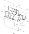
- film capacitor 100 casing 10; positive electrode busbar 20; first electrode terminal 21; first connection sheet 22; first connection terminal 221; first extending portion 23; negative electrode busbar 30; second electrode terminal 31; second connection sheet 32; second connection terminal 321; notch 322; insulation sheet 40; short limb 41; long limb 42; capacitor core 50.
- the terms “mounted,” “supported,” “connected,” and “coupled” and variations thereof are used broadly and encompass such as mechanical or electrical mountings, connections and couplings, also can be inner mountings, connections and couplings of two components, and further can be direct and indirect mountings, connections, and couplings, which can be understood by those skilled in the art according to the detail embodiment of the present disclosure.
- a film capacitor 100 according to embodiments of the present disclosure will be described with reference to drawings.
- the film capacitor 100 may be used in an electric vehicle and includes: a casing 10, a plurality of capacitor cores 50, a positive electrode busbar 20, a negative electrode busbar 30, a first electrode terminal 21 connected to the positive electrode busbar 20, a second electrode terminal 31 connected to the negative electrode busbar 30, a first connection sheet 22 and a second connection sheet 32.
- the plurality of capacitor cores 50, the positive electrode busbar 20, the negative electrode busbar 30, the first connection sheet 22 and the second connection sheet 32 are disposed within the casing 10 and sealed by potting insulators, and the positive electrode busbar 20 and the negative electrode busbar 30 are superposed together and an insulation sheet 40 is provided between the positive electrode busbar 20 and the negative electrode busbar 30.
- the first connection sheet 22 and the second connection sheet 32 are opposed to each other and the capacitor core 50 is disposed between the first connection sheet 22 and the second connection sheet 32, the first connection sheet 22 is connected to the positive electrode busbar 20 and provided with a first connection terminal 221 connected to the capacitor core 50, and the second connection sheet 32 is connected to the negative electrode busbar 30 and provided with a second connection terminal 321 connected to the capacitor core 50.
- the positive electrode busbar 20, the insulation sheet 40 and the negative electrode busbar 30 are superposed together and the insulation sheet 40 is provided between the positive electrode busbar 20 and the negative electrode busbar 30 to make the positive electrode busbar 20 and the negative electrode busbar 30 insulated from each other.
- the first connection sheet 22 may be perpendicularly connected to an edge of the positive electrode busbar 20, and the second connection sheet 32 may be perpendicularly connected to an edge of the negative electrode busbar 30.
- the capacitor core 50 is disposed between the first connection sheet 22 and the second connection sheet 32. That is, the positive electrode busbar 20, the negative electrode busbar 30 and the insulation sheet 40 are all disposed at a side surface of the capacitor core 50.
- the positive electrode busbar 20 is provided with the first electrode terminal 21 and the negative electrode busbar 30 is provided with the second electrode terminal 31.
- the first electrode terminal 21 and the second electrode terminal 31 are connected to a connection terminal of an Insulated Gate Bipolar Transistor (IGBT) respectively.
- IGBT Insulated Gate Bipolar Transistor
- the first connection sheet 22 is provided with the first connection terminal 221, and the first connection terminal 221 is welded with a first end of the capacitor core 50.
- the second connection sheet 32 is provided with the second connection terminal 321, and the second connection terminal 321 is welded with a second end of the capacitor core 50.
- the positive electrode busbar 20 and the negative electrode busbar 30 are disposed within the casing 10, the first connection sheet 22 connected to the positive electrode busbar 20 and the second connection sheet 32 connected to the negative electrode busbar 30 are positioned at the two ends of the capacitor core 50 respectively.
- the first connection sheet 22 and the second connection sheet 32 may be directly connected to the capacitor core 50 in a welding manner, which is convenient for the welding automation, effectively improves the product quality and the manufacturing efficiency and reduces the cost.
- the negative electrode busbar 30, the positive electrode busbar 20 and the insulation sheet 40 are all located at the side surface of the capacitor core 50, inductances between the first electrode terminal 21 and the connection terminal of IGBT and between the second electrode terminal 31 and the connection terminal of IGBT can be effectively reduced.
- the first connection sheet 22, the first connection terminal 221 and the positive electrode busbar 20 are integrally formed; the second connection sheet 32, the second connection terminal 321 and the negative electrode busbar 30 are integrally formed.
- the first connection sheet 22 is a portion of the positive electrode busbar 20, extended outwards from an edge of the positive electrode busbar 20 and perpendicular to the positive electrode busbar 20, and the first connection terminal 221 is a portion of the first connection sheet 22 and extended outwards from the first connection sheet 22.
- the second connection sheet 32 is a portion of the negative electrode busbar 30, extended outwards from an edge of the negative electrode busbar 30 and perpendicular to the negative electrode busbar 30, and the second connection terminal 321 is a portion of the second connection sheet 32 and extended outwards from the second connection sheet 32.
- a plurality of first connection terminals 221 is provided, disposed at a peripheral edge of the first connection sheet 22 and spaced apart from each other.
- a plurality of second connection terminals 321 is provided, disposed at a peripheral edge of the second connection sheet 32 and spaced apart from each other.
- the plurality of the first connection terminals 221 is disposed at the peripheral edge of the first connection sheet 22 and the plurality of the second connection terminals 321 is disposed at the peripheral edge of the second connection sheet 32.
- the plurality of first connection terminals 221 is spaced apart from each other at the peripheral edge of the first connection sheet 22 and the plurality of second connection terminals 321 is spaced apart from each other at the peripheral edge of the second connection sheet 32.
- Each of numbers of the first connection terminals 221 and the second connection terminals 321 may be corresponding to a number of the capacitor cores 50.
- Arrangement positions of the first connection terminals 221 on the first connection sheet 22 may be the same with those of the second connection terminals 321 on the second connection sheet 32, so that both ends of each capacitor core 50 can be connected to the corresponding first connection terminal 221 and second connection terminal 321.
- the first electrode terminal 21 is connected to the positive electrode busbar 20 by a rivet or a screw
- the second electrode terminal 31 is connected to the negative electrode busbar 30 by a rivet or a screw. That is, the first electrode terminal 21 and the second electrode terminal 31 may be connected to the positive electrode busbar 20 and the negative electrode busbar 30 respectively by the rivet or the screw.
- this connection manner is simple and feasible, and convenient to be operated.
- the positive electrode busbar 20 and the negative electrode busbar 30 may be connected to IGBT via a plurality of the first electrode terminals 21 and a plurality of the second electrode terminals 31 respectively.
- the plurality of the first electrode terminals 21 and the plurality of the second electrode terminals 31 are provided to form a plurality of pairs of electrode terminals, and the first electrode terminal 21 is adjacent to the second electrode terminal 31 in each pair.
- the positive electrode busbar 20 is provided with the plurality of the first electrode terminals 21 in a length direction thereof and the negative electrode busbar 30 is provided with the plurality of the second electrode terminals 31 in a length direction thereof, in which each two adjacent electrode terminals, i.e., the first electrode terminal 21 and the second electrode terminal 31 arranged adjacent to the first electrode terminal 21, form a pair, and three pairs of the first electrode terminal 21 and the second electrode terminal 31 may be provided in the whole film capacitor 100 in the length directions of the positive electrode busbar 20 and negative electrode busbar 30.
- the positive electrode busbar 20 and the negative electrode busbar 30 are connected to IGBT via the plurality of the first electrode terminals 21 and the plurality of the second electrode terminals 31 respectively, which further reduces the inductances of the first electrode terminals 21 and the second electrode terminals 31.
- the first electrode terminal 21 is connected to the positive electrode busbar 20
- the second electrode terminal 31 is connected to the negative electrode busbar 30 via the second connection sheet 32.
- the first connection sheet 22 and the positive electrode busbar 20 may be integrally formed, the first connection sheet 22 is formed by bending a portion of the positive electrode busbar 20, and the first electrode terminal 21 is connected to the positive electrode busbar 20.
- the second connection sheet 32 and the negative electrode busbar 30 may be integrally formed, and the second connection sheet 32 is formed by bending a portion of the negative electrode busbar 30.
- the second electrode terminal 31 is connected to the second connection sheet 32 so as to perform a connection with the negative electrode busbar 30. Therefore, the first electrode terminal 21 and the second electrode terminal 31 which having this structure further simplify their connections with the positive electrode busbar 20 and the negative electrode busbar 30, thus further simplifying the assembling procedure so as to improve the production efficiency.
- the insulation sheet 40 has an L shape and includes a short limb 41 and a long limb 42.
- the positive electrode busbar 20 is disposed on an outer surface of the long limb 42 of the insulation sheet 40
- the negative electrode busbar 30 is disposed on an inner surface of the long limb 42 of the insulation sheet 40.
- the outer surface of the insulation sheet 40 is referred to a wall surface of the insulation sheet 40 facing away from a side surface of the capacitor core 50
- the inner surface of the insulation sheet 40 is referred to a wall surface of the insulation sheet 40 facing to a side surface of the capacitor core 50.
- the positive electrode busbar 20 includes a first extending portion 23 extended onto an outer surface of the short limb 41 of the insulation sheet 40, and the first electrode terminal 21 is connected to the first extending portion 23.
- the second connection sheet 32 includes a second extending portion extended onto the outer surface of the short limb 41 of the insulation sheet 40 and adjacent to the first extending portion 23, and the second electrode terminal 31 is connected to the second extending portion.
- the first connection sheet 22 is extended from an edge of a free end of the positive electrode busbar 20 away from the short limb 41
- the second connection sheet 32 is extended from an edge of a free end of the negative electrode busbar 30 adjacent to the short limb 41.
- the first extending portion 23 and the positive electrode busbar 20 are integrally formed, and the second extending portion and the second connection sheet 32 are integrally formed.
- the first extending portion 23 is formed by extending a portion of the positive electrode busbar 20
- the second extending portion is formed by extending a portion of the second connection sheet 32.
- the first connection sheet 22 is disposed at a rear edge of the positive electrode busbar 20 and perpendicular to the positive electrode busbar 20, and the first extending portion 23 is disposed at a front edge of the positive electrode busbar 20 and perpendicular to the positive electrode busbar 20.
- the first extending portion 23 is attached to the outer surface of the short limb 41 of the insulation sheet 40.
- the first electrode terminal 21 is connected to the first extending portion 23.
- the second connection sheet 32 is disposed at a front edge of the negative electrode busbar 30 and perpendicular to the negative electrode busbar 30.
- the second connection sheet 32 is disposed in rear of the short limb 41 of the insulation sheet 40 and at least a portion of the second connection sheet 32 is extended upwards beyond an upper surface of the insulation sheet 40 so as to form the second extending portion.
- the second electrode terminal 31 is connected to the second extending portion.
- the insulation sheet 40 has a reasonable structure, so that it is convenient for the first connection terminal 221 and the second connection terminal 321 to be connected to the positive electrode busbar 20 and the negative electrode busbar 30 respectively.
- the positive electrode busbar 20 includes the first extending portion 23 extended onto the outer surface of the short limb 41 of the insulation sheet 40, and the first electrode terminal 21 is connected to the first extending portion 23.
- the short limb 41 of the insulation sheet 40 has a notch 322 configured to expose a portion of the second connection sheet 32 therefrom and adjacent to the first extending portion 23, and the second electrode terminal 31 is connected to the portion of the second connection sheet 32 exposed from the notch 322.
- the first connection sheet 22 is disposed at the rear edge of the positive electrode busbar 20 and perpendicular to the positive electrode busbar 20
- the first extending portion 23 is disposed at the front edge of the positive electrode busbar 20 and perpendicular to the positive electrode busbar 20.
- the first extending portion 23 is attached to the outer surface of the short limb 41 of the insulation sheet 40.
- the first electrode terminal 21 is connected to the first extending portion 23.
- the second connection sheet 32 is disposed at the front edge of the negative electrode busbar 30 and perpendicular to the negative electrode busbar 30.
- the second connection sheet 32 is disposed in rear of the short limb 41 of the insulation sheet 40.
- the short limb 41 of the insulation sheet 40 has the notch 322 configured to expose the portion of the second connection sheet 32 therefrom and adjacent to the first extending portion 23, so that the second electrode terminal 31 can be arranged adjacent to the corresponding first electrode terminal 21.
- each part of the film capacitor 100 may be reasonably adjusted based on an environment in which it is required to be used.
- each of the positive electrode busbar 20, the negative electrode busbar 30, the first connection sheet 22 and the second connection sheet 32 has a rectangle shape.
- a plurality of the first connection sheets 22 is provided and spaced apart from each other in the length direction of the positive electrode busbar 20, and a plurality of the second connection sheets 32 is provided and spaced apart from each other in the length direction of the negative electrode busbar 30.
Landscapes
- Engineering & Computer Science (AREA)
- Power Engineering (AREA)
- Microelectronics & Electronic Packaging (AREA)
- Manufacturing & Machinery (AREA)
- Fixed Capacitors And Capacitor Manufacturing Machines (AREA)
Applications Claiming Priority (2)
| Application Number | Priority Date | Filing Date | Title |
|---|---|---|---|
| CN201420735558.XU CN204424090U (zh) | 2014-11-28 | 2014-11-28 | 薄膜电容器 |
| PCT/CN2015/095341 WO2016082732A1 (en) | 2014-11-28 | 2015-11-23 | Film capacitor |
Publications (3)
| Publication Number | Publication Date |
|---|---|
| EP3210218A1 EP3210218A1 (en) | 2017-08-30 |
| EP3210218A4 EP3210218A4 (en) | 2017-11-22 |
| EP3210218B1 true EP3210218B1 (en) | 2020-09-16 |
Family
ID=53474437
Family Applications (1)
| Application Number | Title | Priority Date | Filing Date |
|---|---|---|---|
| EP15863747.0A Active EP3210218B1 (en) | 2014-11-28 | 2015-11-23 | Film capacitor |
Country Status (6)
| Country | Link |
|---|---|
| US (1) | US10109426B2 (enExample) |
| EP (1) | EP3210218B1 (enExample) |
| JP (1) | JP6517936B2 (enExample) |
| KR (1) | KR101918460B1 (enExample) |
| CN (1) | CN204424090U (enExample) |
| WO (1) | WO2016082732A1 (enExample) |
Families Citing this family (7)
| Publication number | Priority date | Publication date | Assignee | Title |
|---|---|---|---|---|
| CN204424090U (zh) | 2014-11-28 | 2015-06-24 | 比亚迪股份有限公司 | 薄膜电容器 |
| US11570921B2 (en) * | 2015-06-11 | 2023-01-31 | Tesla, Inc. | Semiconductor device with stacked terminals |
| JP6890233B2 (ja) * | 2016-02-25 | 2021-06-18 | パナソニックIpマネジメント株式会社 | フィルムコンデンサ |
| WO2021157262A1 (ja) * | 2020-02-07 | 2021-08-12 | パナソニックIpマネジメント株式会社 | コンデンサ |
| CN111799729B (zh) * | 2020-05-22 | 2021-09-07 | 北京卫星制造厂有限公司 | 一种宇航用大功率可赋型多层复合汇流条 |
| CN118231143B (zh) * | 2023-03-03 | 2024-12-10 | 比亚迪股份有限公司 | 电器件模组、电机控制器及车辆 |
| CN118522567B (zh) * | 2024-07-19 | 2024-10-29 | 比亚迪股份有限公司 | 电容组件、电机控制器及车辆 |
Family Cites Families (16)
| Publication number | Priority date | Publication date | Assignee | Title |
|---|---|---|---|---|
| JP3914865B2 (ja) | 2002-12-06 | 2007-05-16 | 松下電器産業株式会社 | 金属化フィルムコンデンサ |
| DE102005018172A1 (de) * | 2005-04-19 | 2006-10-26 | Conti Temic Microelectronic Gmbh | Leistungskondensator |
| EP2264726B1 (de) * | 2005-05-02 | 2014-09-10 | Epcos Ag | Kondensator |
| JP2009026928A (ja) * | 2007-07-19 | 2009-02-05 | Soshin Electric Co Ltd | フィルムコンデンサ及びその製造方法 |
| KR100983882B1 (ko) * | 2008-07-07 | 2010-09-27 | 주식회사 뉴인텍 | 커패시터용 부스바 조립방법 및 그 제품 |
| US8193449B2 (en) * | 2008-10-13 | 2012-06-05 | GM Global Technology Operations LLC | Low inductance busbar |
| JP5239989B2 (ja) * | 2009-03-25 | 2013-07-17 | パナソニック株式会社 | ケースモールド型コンデンサ |
| US20110149472A1 (en) * | 2009-12-21 | 2011-06-23 | Nuintek Co., Ltd. | Method of connecting busbars with capacitor and product manufactured by the same method |
| JP2011155138A (ja) * | 2010-01-27 | 2011-08-11 | Shizuki Electric Co Inc | コンデンサ |
| AU2010202125B1 (en) | 2010-05-26 | 2010-09-02 | Takeda Pharmaceutical Company Limited | A method to produce an immunoglobulin preparation with improved yield |
| KR20110135233A (ko) * | 2010-06-10 | 2011-12-16 | 현대자동차주식회사 | 자동차의 인버터용 커패시터 |
| US20130335881A1 (en) * | 2011-03-01 | 2013-12-19 | Toyota Jidosha Kabushiki Kaisha | Capacitor device |
| CN202384178U (zh) * | 2011-12-07 | 2012-08-15 | 厦门法拉电子股份有限公司 | 一种带有内部叠层母排的电容器结构 |
| KR101256347B1 (ko) | 2012-08-14 | 2013-05-02 | 주식회사 뉴인텍 | 케이스 탑재형 병렬형 커패시터 |
| JP6145691B2 (ja) * | 2012-12-10 | 2017-06-14 | パナソニックIpマネジメント株式会社 | ケースモールド型コンデンサ |
| CN204424090U (zh) * | 2014-11-28 | 2015-06-24 | 比亚迪股份有限公司 | 薄膜电容器 |
-
2014
- 2014-11-28 CN CN201420735558.XU patent/CN204424090U/zh not_active Expired - Lifetime
-
2015
- 2015-11-23 EP EP15863747.0A patent/EP3210218B1/en active Active
- 2015-11-23 KR KR1020177012690A patent/KR101918460B1/ko active Active
- 2015-11-23 JP JP2017528526A patent/JP6517936B2/ja active Active
- 2015-11-23 WO PCT/CN2015/095341 patent/WO2016082732A1/en not_active Ceased
-
2017
- 2017-05-23 US US15/603,118 patent/US10109426B2/en active Active
Non-Patent Citations (1)
| Title |
|---|
| None * |
Also Published As
| Publication number | Publication date |
|---|---|
| KR101918460B1 (ko) | 2018-11-15 |
| JP2017535970A (ja) | 2017-11-30 |
| US20170256360A1 (en) | 2017-09-07 |
| US10109426B2 (en) | 2018-10-23 |
| WO2016082732A1 (en) | 2016-06-02 |
| KR20170070126A (ko) | 2017-06-21 |
| EP3210218A4 (en) | 2017-11-22 |
| CN204424090U (zh) | 2015-06-24 |
| EP3210218A1 (en) | 2017-08-30 |
| JP6517936B2 (ja) | 2019-05-22 |
Similar Documents
| Publication | Publication Date | Title |
|---|---|---|
| EP3210218B1 (en) | Film capacitor | |
| US10153089B2 (en) | Thin-film capacitor for electric vehicle | |
| WO2016082731A1 (en) | Film capacitor | |
| US10102975B2 (en) | Film capacitor | |
| CN105702456A (zh) | 薄膜电容器 | |
| JP5828119B2 (ja) | 樹脂封止型コンデンサ | |
| JP2018509745A (ja) | 電気コネクタ及びそれを含むバッテリ | |
| CN105702460B (zh) | 三电平用薄膜电容器 | |
| CN204332694U (zh) | 薄膜电容器 | |
| CN208622612U (zh) | 一种用于汽车电机控制器的电容组件 | |
| CN105702459B (zh) | 三电平用薄膜电容器 | |
| EP3136408B1 (en) | Electric vehicle and capacitor thereof | |
| CN105529189B (zh) | 三电平用薄膜电容器 | |
| CN203895219U (zh) | 三相五柱干式非晶合金变压器角环及其安装总成 |
Legal Events
| Date | Code | Title | Description |
|---|---|---|---|
| STAA | Information on the status of an ep patent application or granted ep patent |
Free format text: STATUS: THE INTERNATIONAL PUBLICATION HAS BEEN MADE |
|
| PUAI | Public reference made under article 153(3) epc to a published international application that has entered the european phase |
Free format text: ORIGINAL CODE: 0009012 |
|
| STAA | Information on the status of an ep patent application or granted ep patent |
Free format text: STATUS: REQUEST FOR EXAMINATION WAS MADE |
|
| 17P | Request for examination filed |
Effective date: 20170523 |
|
| AK | Designated contracting states |
Kind code of ref document: A1 Designated state(s): AL AT BE BG CH CY CZ DE DK EE ES FI FR GB GR HR HU IE IS IT LI LT LU LV MC MK MT NL NO PL PT RO RS SE SI SK SM TR |
|
| AX | Request for extension of the european patent |
Extension state: BA ME |
|
| A4 | Supplementary search report drawn up and despatched |
Effective date: 20171024 |
|
| RIC1 | Information provided on ipc code assigned before grant |
Ipc: H01G 4/228 20060101ALI20171018BHEP Ipc: H01G 4/33 20060101AFI20171018BHEP |
|
| STAA | Information on the status of an ep patent application or granted ep patent |
Free format text: STATUS: EXAMINATION IS IN PROGRESS |
|
| 17Q | First examination report despatched |
Effective date: 20171215 |
|
| DAV | Request for validation of the european patent (deleted) | ||
| DAX | Request for extension of the european patent (deleted) | ||
| GRAP | Despatch of communication of intention to grant a patent |
Free format text: ORIGINAL CODE: EPIDOSNIGR1 |
|
| STAA | Information on the status of an ep patent application or granted ep patent |
Free format text: STATUS: GRANT OF PATENT IS INTENDED |
|
| INTG | Intention to grant announced |
Effective date: 20200408 |
|
| GRAS | Grant fee paid |
Free format text: ORIGINAL CODE: EPIDOSNIGR3 |
|
| GRAA | (expected) grant |
Free format text: ORIGINAL CODE: 0009210 |
|
| STAA | Information on the status of an ep patent application or granted ep patent |
Free format text: STATUS: THE PATENT HAS BEEN GRANTED |
|
| AK | Designated contracting states |
Kind code of ref document: B1 Designated state(s): AL AT BE BG CH CY CZ DE DK EE ES FI FR GB GR HR HU IE IS IT LI LT LU LV MC MK MT NL NO PL PT RO RS SE SI SK SM TR |
|
| REG | Reference to a national code |
Ref country code: GB Ref legal event code: FG4D |
|
| REG | Reference to a national code |
Ref country code: CH Ref legal event code: EP |
|
| REG | Reference to a national code |
Ref country code: DE Ref legal event code: R096 Ref document number: 602015059328 Country of ref document: DE |
|
| REG | Reference to a national code |
Ref country code: IE Ref legal event code: FG4D |
|
| REG | Reference to a national code |
Ref country code: AT Ref legal event code: REF Ref document number: 1314901 Country of ref document: AT Kind code of ref document: T Effective date: 20201015 |
|
| PG25 | Lapsed in a contracting state [announced via postgrant information from national office to epo] |
Ref country code: HR Free format text: LAPSE BECAUSE OF FAILURE TO SUBMIT A TRANSLATION OF THE DESCRIPTION OR TO PAY THE FEE WITHIN THE PRESCRIBED TIME-LIMIT Effective date: 20200916 Ref country code: SE Free format text: LAPSE BECAUSE OF FAILURE TO SUBMIT A TRANSLATION OF THE DESCRIPTION OR TO PAY THE FEE WITHIN THE PRESCRIBED TIME-LIMIT Effective date: 20200916 Ref country code: GR Free format text: LAPSE BECAUSE OF FAILURE TO SUBMIT A TRANSLATION OF THE DESCRIPTION OR TO PAY THE FEE WITHIN THE PRESCRIBED TIME-LIMIT Effective date: 20201217 Ref country code: FI Free format text: LAPSE BECAUSE OF FAILURE TO SUBMIT A TRANSLATION OF THE DESCRIPTION OR TO PAY THE FEE WITHIN THE PRESCRIBED TIME-LIMIT Effective date: 20200916 Ref country code: NO Free format text: LAPSE BECAUSE OF FAILURE TO SUBMIT A TRANSLATION OF THE DESCRIPTION OR TO PAY THE FEE WITHIN THE PRESCRIBED TIME-LIMIT Effective date: 20201216 Ref country code: BG Free format text: LAPSE BECAUSE OF FAILURE TO SUBMIT A TRANSLATION OF THE DESCRIPTION OR TO PAY THE FEE WITHIN THE PRESCRIBED TIME-LIMIT Effective date: 20201216 |
|
| REG | Reference to a national code |
Ref country code: AT Ref legal event code: MK05 Ref document number: 1314901 Country of ref document: AT Kind code of ref document: T Effective date: 20200916 |
|
| REG | Reference to a national code |
Ref country code: NL Ref legal event code: MP Effective date: 20200916 |
|
| PG25 | Lapsed in a contracting state [announced via postgrant information from national office to epo] |
Ref country code: LV Free format text: LAPSE BECAUSE OF FAILURE TO SUBMIT A TRANSLATION OF THE DESCRIPTION OR TO PAY THE FEE WITHIN THE PRESCRIBED TIME-LIMIT Effective date: 20200916 Ref country code: RS Free format text: LAPSE BECAUSE OF FAILURE TO SUBMIT A TRANSLATION OF THE DESCRIPTION OR TO PAY THE FEE WITHIN THE PRESCRIBED TIME-LIMIT Effective date: 20200916 |
|
| REG | Reference to a national code |
Ref country code: LT Ref legal event code: MG4D |
|
| PG25 | Lapsed in a contracting state [announced via postgrant information from national office to epo] |
Ref country code: LT Free format text: LAPSE BECAUSE OF FAILURE TO SUBMIT A TRANSLATION OF THE DESCRIPTION OR TO PAY THE FEE WITHIN THE PRESCRIBED TIME-LIMIT Effective date: 20200916 Ref country code: SM Free format text: LAPSE BECAUSE OF FAILURE TO SUBMIT A TRANSLATION OF THE DESCRIPTION OR TO PAY THE FEE WITHIN THE PRESCRIBED TIME-LIMIT Effective date: 20200916 Ref country code: PT Free format text: LAPSE BECAUSE OF FAILURE TO SUBMIT A TRANSLATION OF THE DESCRIPTION OR TO PAY THE FEE WITHIN THE PRESCRIBED TIME-LIMIT Effective date: 20210118 Ref country code: RO Free format text: LAPSE BECAUSE OF FAILURE TO SUBMIT A TRANSLATION OF THE DESCRIPTION OR TO PAY THE FEE WITHIN THE PRESCRIBED TIME-LIMIT Effective date: 20200916 Ref country code: EE Free format text: LAPSE BECAUSE OF FAILURE TO SUBMIT A TRANSLATION OF THE DESCRIPTION OR TO PAY THE FEE WITHIN THE PRESCRIBED TIME-LIMIT Effective date: 20200916 Ref country code: CZ Free format text: LAPSE BECAUSE OF FAILURE TO SUBMIT A TRANSLATION OF THE DESCRIPTION OR TO PAY THE FEE WITHIN THE PRESCRIBED TIME-LIMIT Effective date: 20200916 |
|
| PG25 | Lapsed in a contracting state [announced via postgrant information from national office to epo] |
Ref country code: PL Free format text: LAPSE BECAUSE OF FAILURE TO SUBMIT A TRANSLATION OF THE DESCRIPTION OR TO PAY THE FEE WITHIN THE PRESCRIBED TIME-LIMIT Effective date: 20200916 Ref country code: IS Free format text: LAPSE BECAUSE OF FAILURE TO SUBMIT A TRANSLATION OF THE DESCRIPTION OR TO PAY THE FEE WITHIN THE PRESCRIBED TIME-LIMIT Effective date: 20210116 Ref country code: AT Free format text: LAPSE BECAUSE OF FAILURE TO SUBMIT A TRANSLATION OF THE DESCRIPTION OR TO PAY THE FEE WITHIN THE PRESCRIBED TIME-LIMIT Effective date: 20200916 Ref country code: AL Free format text: LAPSE BECAUSE OF FAILURE TO SUBMIT A TRANSLATION OF THE DESCRIPTION OR TO PAY THE FEE WITHIN THE PRESCRIBED TIME-LIMIT Effective date: 20200916 Ref country code: ES Free format text: LAPSE BECAUSE OF FAILURE TO SUBMIT A TRANSLATION OF THE DESCRIPTION OR TO PAY THE FEE WITHIN THE PRESCRIBED TIME-LIMIT Effective date: 20200916 |
|
| REG | Reference to a national code |
Ref country code: DE Ref legal event code: R097 Ref document number: 602015059328 Country of ref document: DE |
|
| PG25 | Lapsed in a contracting state [announced via postgrant information from national office to epo] |
Ref country code: SK Free format text: LAPSE BECAUSE OF FAILURE TO SUBMIT A TRANSLATION OF THE DESCRIPTION OR TO PAY THE FEE WITHIN THE PRESCRIBED TIME-LIMIT Effective date: 20200916 Ref country code: MC Free format text: LAPSE BECAUSE OF FAILURE TO SUBMIT A TRANSLATION OF THE DESCRIPTION OR TO PAY THE FEE WITHIN THE PRESCRIBED TIME-LIMIT Effective date: 20200916 |
|
| REG | Reference to a national code |
Ref country code: CH Ref legal event code: PL |
|
| PLBE | No opposition filed within time limit |
Free format text: ORIGINAL CODE: 0009261 |
|
| STAA | Information on the status of an ep patent application or granted ep patent |
Free format text: STATUS: NO OPPOSITION FILED WITHIN TIME LIMIT |
|
| PG25 | Lapsed in a contracting state [announced via postgrant information from national office to epo] |
Ref country code: LU Free format text: LAPSE BECAUSE OF NON-PAYMENT OF DUE FEES Effective date: 20201123 |
|
| REG | Reference to a national code |
Ref country code: BE Ref legal event code: MM Effective date: 20201130 |
|
| 26N | No opposition filed |
Effective date: 20210617 |
|
| PG25 | Lapsed in a contracting state [announced via postgrant information from national office to epo] |
Ref country code: SI Free format text: LAPSE BECAUSE OF FAILURE TO SUBMIT A TRANSLATION OF THE DESCRIPTION OR TO PAY THE FEE WITHIN THE PRESCRIBED TIME-LIMIT Effective date: 20200916 Ref country code: LI Free format text: LAPSE BECAUSE OF NON-PAYMENT OF DUE FEES Effective date: 20201130 Ref country code: DK Free format text: LAPSE BECAUSE OF FAILURE TO SUBMIT A TRANSLATION OF THE DESCRIPTION OR TO PAY THE FEE WITHIN THE PRESCRIBED TIME-LIMIT Effective date: 20200916 Ref country code: CH Free format text: LAPSE BECAUSE OF NON-PAYMENT OF DUE FEES Effective date: 20201130 |
|
| PG25 | Lapsed in a contracting state [announced via postgrant information from national office to epo] |
Ref country code: IT Free format text: LAPSE BECAUSE OF FAILURE TO SUBMIT A TRANSLATION OF THE DESCRIPTION OR TO PAY THE FEE WITHIN THE PRESCRIBED TIME-LIMIT Effective date: 20200916 Ref country code: IE Free format text: LAPSE BECAUSE OF NON-PAYMENT OF DUE FEES Effective date: 20201123 |
|
| PG25 | Lapsed in a contracting state [announced via postgrant information from national office to epo] |
Ref country code: TR Free format text: LAPSE BECAUSE OF FAILURE TO SUBMIT A TRANSLATION OF THE DESCRIPTION OR TO PAY THE FEE WITHIN THE PRESCRIBED TIME-LIMIT Effective date: 20200916 Ref country code: MT Free format text: LAPSE BECAUSE OF FAILURE TO SUBMIT A TRANSLATION OF THE DESCRIPTION OR TO PAY THE FEE WITHIN THE PRESCRIBED TIME-LIMIT Effective date: 20200916 Ref country code: CY Free format text: LAPSE BECAUSE OF FAILURE TO SUBMIT A TRANSLATION OF THE DESCRIPTION OR TO PAY THE FEE WITHIN THE PRESCRIBED TIME-LIMIT Effective date: 20200916 |
|
| PG25 | Lapsed in a contracting state [announced via postgrant information from national office to epo] |
Ref country code: MK Free format text: LAPSE BECAUSE OF FAILURE TO SUBMIT A TRANSLATION OF THE DESCRIPTION OR TO PAY THE FEE WITHIN THE PRESCRIBED TIME-LIMIT Effective date: 20200916 |
|
| PG25 | Lapsed in a contracting state [announced via postgrant information from national office to epo] |
Ref country code: BE Free format text: LAPSE BECAUSE OF NON-PAYMENT OF DUE FEES Effective date: 20201130 |
|
| PG25 | Lapsed in a contracting state [announced via postgrant information from national office to epo] |
Ref country code: NL Free format text: LAPSE BECAUSE OF NON-PAYMENT OF DUE FEES Effective date: 20200923 |
|
| P01 | Opt-out of the competence of the unified patent court (upc) registered |
Effective date: 20230527 |
|
| PGFP | Annual fee paid to national office [announced via postgrant information from national office to epo] |
Ref country code: DE Payment date: 20251118 Year of fee payment: 11 |
|
| PGFP | Annual fee paid to national office [announced via postgrant information from national office to epo] |
Ref country code: GB Payment date: 20251120 Year of fee payment: 11 |
|
| PGFP | Annual fee paid to national office [announced via postgrant information from national office to epo] |
Ref country code: FR Payment date: 20251125 Year of fee payment: 11 |