EP3204232B1 - Druckkopfdüsenanordnung - Google Patents
Druckkopfdüsenanordnung Download PDFInfo
- Publication number
- EP3204232B1 EP3204232B1 EP14903780.6A EP14903780A EP3204232B1 EP 3204232 B1 EP3204232 B1 EP 3204232B1 EP 14903780 A EP14903780 A EP 14903780A EP 3204232 B1 EP3204232 B1 EP 3204232B1
- Authority
- EP
- European Patent Office
- Prior art keywords
- die
- printhead
- printhead die
- carrier
- nozzles
- Prior art date
- Legal status (The legal status is an assumption and is not a legal conclusion. Google has not performed a legal analysis and makes no representation as to the accuracy of the status listed.)
- Not-in-force
Links
- 239000000853 adhesive Substances 0.000 claims description 25
- 230000001070 adhesive effect Effects 0.000 claims description 25
- XUIMIQQOPSSXEZ-UHFFFAOYSA-N Silicon Chemical compound [Si] XUIMIQQOPSSXEZ-UHFFFAOYSA-N 0.000 claims description 20
- 229910052710 silicon Inorganic materials 0.000 claims description 20
- 239000010703 silicon Substances 0.000 claims description 20
- 238000000034 method Methods 0.000 claims description 16
- 238000004519 manufacturing process Methods 0.000 claims description 6
- 235000012431 wafers Nutrition 0.000 description 21
- 238000010586 diagram Methods 0.000 description 8
- 230000008569 process Effects 0.000 description 6
- 238000005286 illumination Methods 0.000 description 4
- 239000000463 material Substances 0.000 description 3
- 238000003860 storage Methods 0.000 description 3
- 238000005520 cutting process Methods 0.000 description 2
- 230000007547 defect Effects 0.000 description 2
- 239000012530 fluid Substances 0.000 description 2
- 230000006870 function Effects 0.000 description 2
- 230000002085 persistent effect Effects 0.000 description 2
- 230000000712 assembly Effects 0.000 description 1
- 238000000429 assembly Methods 0.000 description 1
- 230000002457 bidirectional effect Effects 0.000 description 1
- 238000010276 construction Methods 0.000 description 1
- 230000001419 dependent effect Effects 0.000 description 1
- 238000000151 deposition Methods 0.000 description 1
- 238000005530 etching Methods 0.000 description 1
- 238000010304 firing Methods 0.000 description 1
- 230000000873 masking effect Effects 0.000 description 1
- 230000009467 reduction Effects 0.000 description 1
- 239000000758 substrate Substances 0.000 description 1
- 230000001052 transient effect Effects 0.000 description 1
Images



Classifications
-
- B—PERFORMING OPERATIONS; TRANSPORTING
- B41—PRINTING; LINING MACHINES; TYPEWRITERS; STAMPS
- B41J—TYPEWRITERS; SELECTIVE PRINTING MECHANISMS, i.e. MECHANISMS PRINTING OTHERWISE THAN FROM A FORME; CORRECTION OF TYPOGRAPHICAL ERRORS
- B41J2/00—Typewriters or selective printing mechanisms characterised by the printing or marking process for which they are designed
- B41J2/005—Typewriters or selective printing mechanisms characterised by the printing or marking process for which they are designed characterised by bringing liquid or particles selectively into contact with a printing material
- B41J2/01—Ink jet
- B41J2/135—Nozzles
- B41J2/14—Structure thereof only for on-demand ink jet heads
-
- B—PERFORMING OPERATIONS; TRANSPORTING
- B41—PRINTING; LINING MACHINES; TYPEWRITERS; STAMPS
- B41J—TYPEWRITERS; SELECTIVE PRINTING MECHANISMS, i.e. MECHANISMS PRINTING OTHERWISE THAN FROM A FORME; CORRECTION OF TYPOGRAPHICAL ERRORS
- B41J2/00—Typewriters or selective printing mechanisms characterised by the printing or marking process for which they are designed
- B41J2/005—Typewriters or selective printing mechanisms characterised by the printing or marking process for which they are designed characterised by bringing liquid or particles selectively into contact with a printing material
- B41J2/01—Ink jet
- B41J2/015—Ink jet characterised by the jet generation process
- B41J2/04—Ink jet characterised by the jet generation process generating single droplets or particles on demand
- B41J2/045—Ink jet characterised by the jet generation process generating single droplets or particles on demand by pressure, e.g. electromechanical transducers
- B41J2/04501—Control methods or devices therefor, e.g. driver circuits, control circuits
- B41J2/04505—Control methods or devices therefor, e.g. driver circuits, control circuits aiming at correcting alignment
-
- B—PERFORMING OPERATIONS; TRANSPORTING
- B41—PRINTING; LINING MACHINES; TYPEWRITERS; STAMPS
- B41J—TYPEWRITERS; SELECTIVE PRINTING MECHANISMS, i.e. MECHANISMS PRINTING OTHERWISE THAN FROM A FORME; CORRECTION OF TYPOGRAPHICAL ERRORS
- B41J2/00—Typewriters or selective printing mechanisms characterised by the printing or marking process for which they are designed
- B41J2/005—Typewriters or selective printing mechanisms characterised by the printing or marking process for which they are designed characterised by bringing liquid or particles selectively into contact with a printing material
- B41J2/01—Ink jet
- B41J2/015—Ink jet characterised by the jet generation process
- B41J2/04—Ink jet characterised by the jet generation process generating single droplets or particles on demand
- B41J2/045—Ink jet characterised by the jet generation process generating single droplets or particles on demand by pressure, e.g. electromechanical transducers
- B41J2/04501—Control methods or devices therefor, e.g. driver circuits, control circuits
- B41J2/04506—Control methods or devices therefor, e.g. driver circuits, control circuits aiming at correcting manufacturing tolerances
-
- B—PERFORMING OPERATIONS; TRANSPORTING
- B41—PRINTING; LINING MACHINES; TYPEWRITERS; STAMPS
- B41J—TYPEWRITERS; SELECTIVE PRINTING MECHANISMS, i.e. MECHANISMS PRINTING OTHERWISE THAN FROM A FORME; CORRECTION OF TYPOGRAPHICAL ERRORS
- B41J2/00—Typewriters or selective printing mechanisms characterised by the printing or marking process for which they are designed
- B41J2/005—Typewriters or selective printing mechanisms characterised by the printing or marking process for which they are designed characterised by bringing liquid or particles selectively into contact with a printing material
- B41J2/01—Ink jet
- B41J2/015—Ink jet characterised by the jet generation process
- B41J2/04—Ink jet characterised by the jet generation process generating single droplets or particles on demand
- B41J2/045—Ink jet characterised by the jet generation process generating single droplets or particles on demand by pressure, e.g. electromechanical transducers
- B41J2/04501—Control methods or devices therefor, e.g. driver circuits, control circuits
- B41J2/04581—Control methods or devices therefor, e.g. driver circuits, control circuits controlling heads based on piezoelectric elements
-
- B—PERFORMING OPERATIONS; TRANSPORTING
- B41—PRINTING; LINING MACHINES; TYPEWRITERS; STAMPS
- B41J—TYPEWRITERS; SELECTIVE PRINTING MECHANISMS, i.e. MECHANISMS PRINTING OTHERWISE THAN FROM A FORME; CORRECTION OF TYPOGRAPHICAL ERRORS
- B41J2/00—Typewriters or selective printing mechanisms characterised by the printing or marking process for which they are designed
- B41J2/005—Typewriters or selective printing mechanisms characterised by the printing or marking process for which they are designed characterised by bringing liquid or particles selectively into contact with a printing material
- B41J2/01—Ink jet
- B41J2/135—Nozzles
- B41J2/14—Structure thereof only for on-demand ink jet heads
- B41J2/14201—Structure of print heads with piezoelectric elements
-
- B—PERFORMING OPERATIONS; TRANSPORTING
- B41—PRINTING; LINING MACHINES; TYPEWRITERS; STAMPS
- B41J—TYPEWRITERS; SELECTIVE PRINTING MECHANISMS, i.e. MECHANISMS PRINTING OTHERWISE THAN FROM A FORME; CORRECTION OF TYPOGRAPHICAL ERRORS
- B41J2/00—Typewriters or selective printing mechanisms characterised by the printing or marking process for which they are designed
- B41J2/005—Typewriters or selective printing mechanisms characterised by the printing or marking process for which they are designed characterised by bringing liquid or particles selectively into contact with a printing material
- B41J2/01—Ink jet
- B41J2/135—Nozzles
- B41J2/16—Production of nozzles
- B41J2/1601—Production of bubble jet print heads
- B41J2/1604—Production of bubble jet print heads of the edge shooter type
-
- B—PERFORMING OPERATIONS; TRANSPORTING
- B41—PRINTING; LINING MACHINES; TYPEWRITERS; STAMPS
- B41J—TYPEWRITERS; SELECTIVE PRINTING MECHANISMS, i.e. MECHANISMS PRINTING OTHERWISE THAN FROM A FORME; CORRECTION OF TYPOGRAPHICAL ERRORS
- B41J25/00—Actions or mechanisms not otherwise provided for
- B41J25/001—Mechanisms for bodily moving print heads or carriages parallel to the paper surface
-
- B—PERFORMING OPERATIONS; TRANSPORTING
- B41—PRINTING; LINING MACHINES; TYPEWRITERS; STAMPS
- B41J—TYPEWRITERS; SELECTIVE PRINTING MECHANISMS, i.e. MECHANISMS PRINTING OTHERWISE THAN FROM A FORME; CORRECTION OF TYPOGRAPHICAL ERRORS
- B41J25/00—Actions or mechanisms not otherwise provided for
- B41J25/34—Bodily-changeable print heads or carriages
-
- B—PERFORMING OPERATIONS; TRANSPORTING
- B41—PRINTING; LINING MACHINES; TYPEWRITERS; STAMPS
- B41J—TYPEWRITERS; SELECTIVE PRINTING MECHANISMS, i.e. MECHANISMS PRINTING OTHERWISE THAN FROM A FORME; CORRECTION OF TYPOGRAPHICAL ERRORS
- B41J2/00—Typewriters or selective printing mechanisms characterised by the printing or marking process for which they are designed
- B41J2/005—Typewriters or selective printing mechanisms characterised by the printing or marking process for which they are designed characterised by bringing liquid or particles selectively into contact with a printing material
- B41J2/01—Ink jet
- B41J2/135—Nozzles
- B41J2/14—Structure thereof only for on-demand ink jet heads
- B41J2002/14379—Edge shooter
-
- B—PERFORMING OPERATIONS; TRANSPORTING
- B41—PRINTING; LINING MACHINES; TYPEWRITERS; STAMPS
- B41J—TYPEWRITERS; SELECTIVE PRINTING MECHANISMS, i.e. MECHANISMS PRINTING OTHERWISE THAN FROM A FORME; CORRECTION OF TYPOGRAPHICAL ERRORS
- B41J2202/00—Embodiments of or processes related to ink-jet or thermal heads
- B41J2202/01—Embodiments of or processes related to ink-jet heads
- B41J2202/19—Assembling head units
Definitions
- Current piezoelectric printheads manufactured for use in commercial printers may utilize double-sided silicon die in order to provide multiple ink drop weights and high nozzle densities.
- the double-sided die are manufactured by using a photolithographic and etch process to build piezoelectric actuator circuits and fluidic channels for ink dispensing devices on both sides of a silicon wafer. The wafer is then separated into individual double-sided die. The devices manufactured on one side of the silicon wafer must be protected while devices are manufactured on the other side of the silicon wafer, resulting in increased complexity of the manufacturing process and lower yields from each silicon wafer.
- US2005/062799A1 discloses a method of assembling an ink jet head unit.
- WO2011/002747 discloses an apparatus to enable mounting first and second jetting assemblies on a frame.
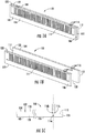
- Figures 1A, 1B, and 1C illustrate an example printhead die assembly 100.
- Figure 1A is a perspective view of printhead die assembly 100.
- Figure 1B is an exploded view of printhead die assembly 100.
- Figure 1C is a top plan view of printhead die assembly 100.
- Printhead die assembly 100 may be, for example, a die assembly for use in a piezoelectric inkjet printhead similar to printheads used in commercial inkjet printers, such as the SCITEX FB10000 manufactured by Hewlett Packard Company, assignee of the present application.
- Printhead die assembly 100 may be used in other types of printheads and/or printers as well.
- printhead die assembly 100 may include a die 102 and a die 104.
- Die 102 and die 104 are shown as rectangular in shape, but other shapes are contemplated as well, depending on the particular application.
- Example dimensions for rectangular die 102 and die 104 are 1.5 inches in length by 0.25 inches in width, but other dimensions and sizes are contemplated as well, depending on the particular application.
- Die 102 and die 104 may be manufactured from, for example, a silicon wafer or another suitable material, depending on the particular application.
- die 102 and die 104 may be individual die sections separated (e.g., by sawing or cutting) from an 8 inch diameter round silicon wafer having an industry standard thickness of approximately 757 microns. If example dimensions of 1.5 inches in length by 0.25 inches in width are used for each die, then approximately 96 die may be cut from a single 8 inch diameter silicon wafer. Other wafer sizes and thicknesses are contemplated as well, depending on the particular application.
- Die 102 may have a surface 106 and an opposite surface 108.
- die 104 may have a surface 110 and an opposite surface 112.
- surface 106 of die 102 and surface 110 of die 104 may have ink dispensing devices 114 constructed thereon.
- Ink dispensing devices 114 may include, for example, fluid chambers and piezoelectric actuators for dispensing ink through nozzles 116.
- Ink dispensing devices 114 may be constructed on surfaces 106 and 110 using, for example, a photolithographic process that uses a combination of masking, depositing, and etching steps in order to form electrical circuits, fluidic channels, and other structures that make up the ink dispensing devices 114 for each die on the front surface of a silicon wafer. Individual die, such as die 102 and die 104, may then be separated from the other die on the silicon wafer. By way of example, if dimensions of 1.5 inches in length by 0.25 inches in width are used for each die, then approximately 96 die may be cut from a single 8 inch diameter, 757 micron silicon wafer, where each die includes 96 ink dispensing devices 116 each having a corresponding nozzle 116.
- ink dispensing devices 114 Other manufacturing processes may be used as well to create ink dispensing devices 114 depending on the particular application. Similarly, die having differing types, numbers, and sizes of ink dispensing devices 114 and nozzles 116 are contemplated as well, depending on the particular application.
- die 102 and die 104 may be positioned adjacent to each other.
- die 102 and die 104 may be positioned so that surface 108 of die 102 faces surface 112 of die 104.
- die 102 and die 104 may be positioned so that a surface 120 of die 102 containing openings for nozzles 116 may be approximately flush with a surface 122 of die 104 that also contains openings for nozzles 116.
- a layer of adhesive may be applied between die 102 and die 104.
- an ultraviolet (UV) curing adhesive may be applied to one or both of surfaces 108 and 112 to hold die 102 and die 104 in positions adjacent to each other when surfaces 108 and 112 are mated. Once die 102 and 104 are positioned and aligned as desired, the layer of adhesive may be exposed to UV illumination in order to set the adhesive and fix die 102 and die 104 in position.
- UV ultraviolet
- Figure 1C is top plan view of printhead die assembly 100 that illustrates an example positioning of die 102 with respect to die 104.
- die 102 and die 104 may be positioned so that nozzles 116 of die 102 are aligned relative to nozzles 116 of die 104.
- a nozzle 116a of die 102 is shown as being centered with respect to nozzles 116b and 116c of die 104. While the example illustrated in Figure 1C shows a centered alignment, other alignments or offsets are contemplated as well, depending on the particular application.
- nozzles 116a, 116b, and 116c may be aligned with respect to each other with an accuracy of approximately 5 microns.
- die 102 and die 104 may be-single sided die, as opposed to double-sided die.
- Die 102 and die 104 are single sided die in the sense that they include electrical circuits, fluidic channels, and other structures that make up the ink dispensing devices 114 on only one of surfaces 106 and 108 with respect to die 102, and on only one of surfaces 110 and 112 with respect to die 104. That is, as best shown in Figure 1B , die 102 may include ink dispensing devices 114 constructed on surface 106, but not on opposite surface 110, and die 104 may include ink dispensing devices 114 constructed on surface 110, but not on opposite surface 112. Using two single-sided die in die assembly 102 allows for multiple drop weights, high nozzle density, low crosstalk, and higher reliability.
- Using two single-sided die in die assembly 100 as opposed to one double-sided die also eliminates the need to construct ink dispensing devices 114 on both sides of a die found on a double-sided printhead die. Constructing ink dispensing devices on both sides of a die requires that the devices manufactured on one side of, for example, a silicon wafer be protected while ink dispensing devices are manufactured on the other side of the silicon wafer. For example, where photolithographic processes are used, a sacrificial layer is often used to protect devices formed on one side of the silicon wafer while devices are constructed on the opposite side, resulting in increased complexity of the photolithographic device construction process.
- This process can also lead to a large number of device defects, lower die yields from each silicon wafer, increased manufacturing variation, and poor image quality.
- Using two single-sided die in die assembly 100 as opposed to one double-sided die may eliminate the need for such a sacrificial layer, thus reducing the complexity of the photolithographic process.
- Using two single-sided die in die assembly 100 as opposed to one double-sided die also reduces number of defects associated with using a sacrificial layer for protection of devices formed on one side of the silicon wafer while devices are constructed on the opposite side, resulting in higher die yields, reduced manufacturing variation, and higher image quality.
- Using two single-sided die in die assembly 102 also allows for thinner wafers of industry standard thickness (e.g., 725 microns) to be used, as opposed to thicker non-standard wafers that are used in double-sided die (e.g., 1061 microns), which may provide material cost reductions and manufacturing efficiencies.
- industry standard thickness e.g. 725 microns
- thicker non-standard wafers e.g., 1061 microns
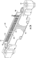
- Figures 2A and 2B illustrate an example printhead assembly 200 including an example printhead die assembly 202.
- Figure 2A is a perspective view of example printhead 200.
- Figure 2B is a bottom view of the example printhead 200.
- Printhead 200 may be, for example, a piezoelectric inkjet printhead similar to printheads used in commercial inkjet printers, such as the SCITEX FB10000 manufactured by Hewlett Packard Company, assignee of the present application. Printhead 200 may also be designed for use in other types of printers as well.
- Printhead die assembly 202 is similar to printhead die assembly 100 shown in Figure 1A .
- printhead die assembly 202 may include a die 204 and a die 206.
- Die 204 and die 206 are shown as rectangular in shape, but other shapes, dimensions and sizes are contemplated as well, depending on the particular application.
- Die 204 and die 206 may be manufactured from, for example, a silicon wafer or another suitable material, depending on the particular application.
- die 102 and die 104 may be individual die sections separated (e.g., by sawing or cutting) from an 8 inch diameter round silicon wafer having an industry standard thickness of approximately 725 microns.
- a surface 208 of die 204 and a surface 212 of die 206 may each have ink dispensing devices 216 constructed thereon.
- Ink dispensing devices 216 may include, for example, fluid chambers and piezoelectric actuators for dispensing ink through nozzles 218.
- die 204 and die 206 may be positioned adjacent to each other.
- die 204 and die 206 may be positioned so that the surface of die 204 opposite surface 208 faces a surface of die 206 opposite surface 212.
- a layer of adhesive may be applied between die 204 and die 206.
- die 204 and die 206 may be positioned so that nozzles 218 of die 204 are aligned relative to nozzles 218 of die 206 (e.g., a centered alignment, other alignments or offsets) depending on the particular application.
- Die 204 and die 206 may be single sided die, as opposed to double-sided die.
- Printhead 200 may also include a die carrier 230.
- Die carrier 230 may provide electrical and fluidic connections between printhead die assembly 202 and, for example, a commercial inkjet printer.
- Die carrier 230 may also provide structural support for printhead die assembly 202.
- printhead die assembly 202 may be partially inserted into and seated within a cavity of die carrier 230 such that die 204 and die 206 are generally held in position, with portions of printhead die assembly extending outward from die carrier 230 such that nozzles 218 are exposed.
- Die carrier 230 may include a registration pin 232.
- Registration pin 232 may be used to provide a reference point from which the position of printhead die assembly may be defined, such as for calibrating a printer in which printhead 230 is used.
- registration pin 230 may be used to align die 204 and die 206 within die carrier 230.
- a nozzle 218a of die 204 and a nozzle 218b of die 206 may each be aligned with registration pin 232 based on a line 234 passing through the center of registration pin 232.
- the individual positions of die 204 and die 206 may be adjusted such that, for example, the centers of nozzles 218a and 218b are a particular distance from line 234.
- nozzles 218a and 218b may be aligned with registration pin 232 with an accuracy of approximately 8 microns.
- Figure 3 is a perspective view of an example printhead 300 illustrating an example of how an adhesive may be used to fix the position of a printhead die assembly within a die carrier.
- Printhead 300 may be similar to, for example, printhead 200 shown in Figure 2A .
- printhead 302 may include a printhead die assembly 302 that includes a die 304 and a die 306.
- Printhead 302 may also include a die carrier 330 and a registration pin 332.
- an adhesive 334 may be applied such that it is in contact with die 304, die 306, and die carrier 330 to fix the position of die 304 and die 306 within die carrier 330.
- Adhesive 334 may be, for example, a UV adhesive or another suitable adhesive.
- a UV adhesive may be applied as shown in Figure 3 during or after alignment of die 304 and die 306 with registration pin 332, and may then be exposed to UV illumination in order to set adhesive 334 and fix the position of die 304 and die 306 within die carrier 330.
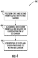
- Figure 4 is a flow diagram illustrating an example method of assembling a printhead.
- the printhead may be, for example, printhead 200 shown in Figure 2A and 2B or printhead 300 shown in Figure 3 .
- the printhead may include a printhead die assembly with two printhead die, and may also include a die carrier and a registration pin as described with reference to printhead 200 or printhead 300 and Figures 2A , 2B, and 3 .
- each of the printhead die may be inserted into the die carrier.
- each of the printhead die may be aligned relative to the registration pin of the die carrier.
- a nozzle of each printhead die may be aligned with the registration pin.
- a nozzle of each printhead die may each be aligned with the registration pin with an accuracy of approximately 8 microns.
- nozzles of each of the printhead die may also be aligned relative to each other.
- nozzles of each of the printhead die may also be aligned relative to each other with an accuracy of approximately 5 microns.
- the desired level of accuracy may be achieved using a die alignment tool having two motorized stages coupled to micro grippers.
- the die alignment tool may utilize a real-time image processing and optics tool to acquire the position of each printhead die and control the movement of the motorized stages with a repeatability of less than 1 micron and an accuracy of not less than 1.5 microns.
- the position of each of the printhead die may be fixed within the die carrier.
- an adhesive may be applied such that it is in contact with each of the printhead die and the die carrier to fix the position of each printhead die within the die carrier.
- the adhesive may be, for example, a UV adhesive or another suitable adhesive.
- a UV adhesive may be applied during or after alignment of each printhead die with the registration pin, and may then be exposed to UV illumination in order to set the adhesive and fix the position of each printhead die within the die carrier.
- a layer of adhesive may be applied between the two printhead die.
- a UV adhesive may also be applied between each of the printhead die prior to step 402 in order to hold each of the printhead die in positions adjacent to each other when mated together. Once each of the printhead die are positioned and aligned as desired, the layer of adhesive may be exposed to UV illumination in order to set the adhesive and fix each of the printhead die in position.
- FIG 5 is a block diagram illustrating an example system 500 for calibrating a printhead.
- System 500 may be implemented in, for example, a commercial inkjet printer, such as the SCITEX FB10000 manufactured by Hewlett Packard Company, assignee of the present application, or may be a separate system or a combination thereof.
- the printhead may be, for example, printhead 200 shown in Figure 2A and 2B or printhead 300 shown in Figure 3 .
- the printhead may include a printhead die assembly with two printhead die, and may also include a die carrier and a registration pin as described with reference to printhead 200 or printhead 300 and Figures 2A , 2B, and 3 .
- System 500 may allow users to calibrate printheads having a printhead die assembly with two printhead die.
- system 500 may allow users to minimize the variability of ink drop firing conditions in order to provide the desired image quality. Variations in ink drop size and velocity, and/or nominal nozzle positioning of different printheads may result in non-uniform output, grainy or noisy fill areas, and/or poor image quality.
- System 500 may allow users to separately calibrate the operating voltage of each of the printhead die in the printhead as well as an entire array of printheads.
- System 500 may include processor 502 and memory 504.
- Processor 502 may include a single processing unit or distributed processing units configured to carry out instructions contained in memory 504. In general, following instructions contained in memory 504, processor 502 may allow users to separately calibrate the operating voltage of each printhead die as well as an entire array of printheads.
- the term "processing unit” shall mean a presently developed or future developed processing unit that executes sequences of instructions contained in a memory. Execution of the sequences of instructions causes the processing unit to perform steps such as generating control signals.
- the instructions may be loaded in a random access memory (RAM) for execution by the processing unit from a read only memory (ROM), a mass storage device, or some other persistent storage.
- RAM random access memory
- ROM read only memory
- mass storage device or some other persistent storage.
- system 500 may be implemented entirely or in part by one or more application-specific integrated circuits (ASICs).
- ASICs application-specific integrated circuits
- Memory 504 may include a non-transient computer-readable medium or other persistent storage device, volatile memory such as DRAM, or some combination of these; for example a hard disk combined with RAM. Memory 504 may contain instructions for directing the carrying out of functions and analysis by processor 502. In some implementations, memory 504 may further store data for use by processor 502. Memory 504 may store various software or code modules that direct processor 502 to carry out various interrelated actions. In the example illustrated, memory 504 includes a calibration pattern module 510, an acquisition module 520, an analysis module 530, and an adjustment module 540. In some examples, modules 510, 520, 530, and 540 may be combined or distributed into additional or fewer modules. Modules 510, 520, 530, and 540 may cooperate to direct processor 502 to carry out a method 600 set forth by the flow diagram of Figure 6 .
- calibration patterns may be generated for each of two printhead die in a printhead by module 510.
- the calibration patterns may, for example, be printed by a printer in which the printhead is installed.
- Figure 7 is a diagram illustrating an example printhead calibration pattern 700 generated using module 510. As shown in Figure 7 , multiple calibration patches may be generated for each printhead die by varying the operating voltage of each printhead die. Bidirectional lines may printed a various printing conditions, and a fiducial may indicate the print head side position and may be used to determine and calibrate errors.
- the calibration patterns generated in step 602 for each printhead die may be acquired by acquisition module 520.
- acquisition module 520 may direct processor 502 to scan the printed calibration patters into an electronic format that may be analyzed by system 500.
- the calibration patterns generated in step 602 for each printhead die may be analyzed by analysis module 530.
- analysis module may analyze properties such as the physical distance between the two dies or nozzle column spacing, die tilt, die height, print axis velocity, target drop velocity, an offset from the target drop velocity, a nominal printing height, the distance it takes an ink drop to pass from ejection to substrate, etc.
- operating voltages for each printhead die may be adjusted by adjustment module 540 based on the analysis in step 606. These adjustments may result in performance image quality improvements such as, for example, improved uniformity, more uniform drop weights, improved drop positioning, and correction of nozzle space errors, tilting, and die height differences.
Landscapes
- Engineering & Computer Science (AREA)
- Manufacturing & Machinery (AREA)
- Particle Formation And Scattering Control In Inkjet Printers (AREA)
- Ink Jet (AREA)
Claims (7)
- Druckkopf (200, 300), der Folgendes umfasst:einen ersten und einen zweiten Druckkopfchip (204, 206; 304, 306), wobei jeder des ersten und des zweiten Druckkopfchips (204, 206; 304, 306) eine jeweilige erste Oberfläche (208, 212), die darauf eingerichtete Tintenausgabevorrichtungen (216) beinhaltet, und eine jeweilige zweite Oberfläche gegenüber der ersten Oberfläche (208, 212) aufweist, und wobei jeder des ersten und des zweiten Druckkopfchips (204, 206; 304, 306) Düsen (218) für die Tintenausgabevorrichtungen (216) beinhaltet; undeinen Chipträger (230; 330), der einen Passungsstift (232; 332) aufweist,wobei der erste und der zweite Druckkopfchip (204, 206; 304, 306) teilweise eingesetzt in einem Hohlraum des Chipträgers (230; 330) positioniert sind und in diesem so sitzen, dass der erste und der zweite Druckkopfchip (204, 206; 304, 306) im Allgemeinen in Position gehalten werden, wobei die zweite Oberfläche des ersten Druckkopfchips (204; 304) der zweiten Oberfläche des zweiten Druckkopfchips (206; 306) zugewandt ist und sich Abschnitte des ersten und des zweiten Druckkopfchips (204, 206; 304, 306) von dem Chipträger (230; 330) nach außen erstrecken, so dass die Düsen (218) freigelegt sind,wobei sich der Passungsstift (232; 332) in einer axialen Richtung parallel zu einer Richtung erstreckt, der die Düsen (218) zugewandt sind,wobei der erste und der zweite Druckkopfchip (204, 206; 304, 306) relativ zu dem Passungsstift (232; 332) so ausgerichtet sind, dass sich die Düsenmitten des ersten und des zweiten Druckkopfchips (204, 206; 304, 306) in einem bestimmten Abstand von einer Linie (234) befinden, die in der axialen Richtung gesehen durch die Mitte des Passungsstifts (232) verläuft, undgekennzeichnet durch einen Klebstoff (334), der mit jedem des ersten und des zweiten Druckkopfchips (204, 206; 304, 306) und mit dem Chipträger (230; 330) in Berührung steht, um die Position des ersten und des zweiten Druckkopfchips (204, 206; 304, 306) in dem Chipträger (230; 330) zu fixieren.
- Druckkopf nach Anspruch 1, wobei der erste und der zweite Druckkopfchip (204, 206; 304, 306) Siliziumscheibenbereiche beinhalten, auf denen die Tintenausgabevorrichtungen eingerichtet sind.
- Verfahren (400), das Folgendes umfasst:Positionieren (402) des ersten und des zweiten Druckkopfchips (204, 206; 304, 306) in einem Hohlraum eines Chipträgers (230; 330), wobei jeder des ersten und des zweiten Druckkopfchips (204, 206; 304, 306) eine jeweilige erste Oberfläche (208, 212), die darauf eingerichtete Tintenausgabevorrichtungen (216) beinhaltet, und eine jeweilige zweite Oberfläche gegenüber der ersten Oberfläche (208, 212) aufweist, und wobei jeder des ersten und des zweiten Druckkopfchips (204, 206; 304, 306) Düsen (218) für die Tintenausgabevorrichtungen (216) beinhaltet, wobei der erste und der zweite Druckkopfchip (204, 206; 304, 306) teilweise eingesetzt in dem Hohlraum des Chipträgers (230; 330) positioniert sind und in diesem so sitzen, dass der erste und der zweite Druckkopfchip (204, 206; 304, 306) im Allgemeinen in Position gehalten werden, wobei die zweite Oberfläche des ersten Druckkopfchips (204; 304) der zweiten Oberfläche des zweiten Druckkopfchips (206; 306) zugewandt ist und sich Abschnitte des ersten und des zweiten Druckkopfchips (204, 206; 304, 306) von dem Chipträger (230) nach außen erstrecken, so dass die Düsen (218) freigelegt sind, und wobei der Chipträger (230; 330) einen Passungsstift (232; 332) aufweist, der sich in einer axialen Richtung parallel zu einer Richtung, der die Düsen (218) des ersten und des zweiten Druckkopfchips (204, 206; 304, 306) zugewandt sind, erstreckt;Ausrichten (404) des ersten und des zweiten Druckkopfchips (204, 206; 304, 306) relativ zu einem Passungsstift (232; 332) des Chipträgers (230; 330) durch Anpassen der Position des ersten und des zweiten Druckkopfchips (204, 206; 304, 306), so dass sich die Düsenmitten des ersten und des zweiten Druckkopfchips (204, 206; 304, 306) in einem bestimmten Abstand von einer Linie (234) befinden, die in der axialen Richtung gesehen durch die Mitte des Passungsstifts (232; 332) verläuft; undgekennzeichnet durch Aufbringen eines Klebstoffs in Berührung mit jedem des ersten und des zweiten Druckkopfchips (204, 206; 304, 306) und mit dem Chipträger (230), um die Position des ersten und des zweiten Druckkopfchips (204, 206; 304, 306) in dem Chipträger (230; 330) zu fixieren (406).
- Verfahren nach Anspruch 3, das ferner ein Herstellen des ersten und des zweiten Druckkopfchips (204, 206; 304, 306) aus einer Siliziumscheibe umfasst.
- Verfahren nach Anspruch 3, das ferner ein Kalibrieren einer separaten Betriebsspannung für jeden des ersten und des zweiten Druckkopfchips (204, 206; 304, 306) umfasst.
- Verfahren nach Anspruch 5, das ferner ein Analysieren eines unter Verwendung des ersten Druckkopfchips (204; 304) erzeugten ersten Kalibrierungsmusters und eines unter Verwendung des zweiten Druckkopfchips (206; 306) erzeugten zweiten Kalibrierungsmusters umfasst, wobei die Betriebsspannung für jeden des ersten und des zweiten Druckkopfchips (204, 206; 304, 306) variiert wird, um das erste und das zweite Kalibrierungsmuster zu erzeugen.
- Verfahren nach Anspruch 3, wobei die Position des ersten und des zweiten Druckkopfchips (204, 206; 304, 306) unter Verwendung eines Echtzeit-Bildverarbeitungs- und Optikwerkzeugs erfasst wird.
Applications Claiming Priority (1)
| Application Number | Priority Date | Filing Date | Title |
|---|---|---|---|
| PCT/US2014/059335 WO2016057015A1 (en) | 2014-10-06 | 2014-10-06 | Printhead die assembly |
Publications (3)
| Publication Number | Publication Date |
|---|---|
| EP3204232A1 EP3204232A1 (de) | 2017-08-16 |
| EP3204232A4 EP3204232A4 (de) | 2018-05-02 |
| EP3204232B1 true EP3204232B1 (de) | 2021-01-20 |
Family
ID=55653471
Family Applications (1)
| Application Number | Title | Priority Date | Filing Date |
|---|---|---|---|
| EP14903780.6A Not-in-force EP3204232B1 (de) | 2014-10-06 | 2014-10-06 | Druckkopfdüsenanordnung |
Country Status (6)
| Country | Link |
|---|---|
| US (3) | US20170217171A1 (de) |
| EP (1) | EP3204232B1 (de) |
| JP (1) | JP6431611B2 (de) |
| KR (1) | KR102234779B1 (de) |
| CN (1) | CN107000436B (de) |
| WO (1) | WO2016057015A1 (de) |
Citations (1)
| Publication number | Priority date | Publication date | Assignee | Title |
|---|---|---|---|---|
| WO2011002747A2 (en) * | 2009-07-02 | 2011-01-06 | Fujifilm Dimatix, Inc. | Positioning jetting assemblies |
Family Cites Families (32)
| Publication number | Priority date | Publication date | Assignee | Title |
|---|---|---|---|---|
| US5198054A (en) * | 1991-08-12 | 1993-03-30 | Xerox Corporation | Method of making compensated collinear reading or writing bar arrays assembled from subunits |
| US5764257A (en) * | 1991-12-26 | 1998-06-09 | Seiko Epson Corporation | Ink jet recording head |
| US5734394A (en) * | 1995-01-20 | 1998-03-31 | Hewlett-Packard | Kinematically fixing flex circuit to PWA printbar |
| WO1998042514A1 (en) * | 1997-03-26 | 1998-10-01 | Seiko Epson Corporation | Ink jet head, its manufacturing method and ink jet recorder |
| US6742883B1 (en) * | 1997-03-28 | 2004-06-01 | Brother Kogyo Kabushiki Kaisha | Ink jet head capable of reliably removing air bubbles from ink |
| DE69820636T2 (de) * | 1997-08-22 | 2004-11-11 | Xaar Technology Ltd. | Herstellungsverfahren eines druckers |
| JPH11165414A (ja) * | 1997-12-04 | 1999-06-22 | Canon Inc | インクジェット記録ヘッドおよびインクジェット記録装置 |
| JP2001096753A (ja) * | 1999-10-01 | 2001-04-10 | Seiko Epson Corp | インクジェットヘッドの製造方法 |
| JP2001310463A (ja) * | 2000-04-27 | 2001-11-06 | Ricoh Co Ltd | インクジェットヘッド及びその製造方法 |
| JP2001341298A (ja) * | 2000-05-31 | 2001-12-11 | Seiko Instruments Inc | ヘッドチップ及びヘッドユニット |
| WO2003080345A1 (en) * | 2002-03-25 | 2003-10-02 | Olympus Corporation | Method of assembling ink jet head unit |
| JP2004058277A (ja) * | 2002-07-24 | 2004-02-26 | Olympus Corp | インクジェットヘッド及びインクジェットヘッドユニット |
| WO2005065951A1 (ja) * | 2004-01-07 | 2005-07-21 | Hewlett-Packard Industrial Printing Ltd. | インクジェット記録ヘッド |
| JP4995470B2 (ja) * | 2005-07-20 | 2012-08-08 | エスアイアイ・プリンテック株式会社 | インクジェットヘッドおよびインクジェット記録装置 |
| JP2007090690A (ja) * | 2005-09-29 | 2007-04-12 | Konica Minolta Holdings Inc | ラインヘッド及びインクジェット印画装置 |
| US8539586B2 (en) | 2006-05-19 | 2013-09-17 | Peter R. Stephenson | Method for evaluating system risk |
| US8556389B2 (en) * | 2011-02-04 | 2013-10-15 | Kateeva, Inc. | Low-profile MEMS thermal printhead die having backside electrical connections |
| EP2382096B1 (de) * | 2009-01-28 | 2019-12-18 | Hewlett-Packard Development Company, L.P. | Überlappendes drucken |
| JP2010264700A (ja) * | 2009-05-15 | 2010-11-25 | Seiko Epson Corp | 液体噴射ヘッドユニットの製造方法及び液体噴射装置 |
| US8096640B2 (en) * | 2009-05-27 | 2012-01-17 | Hewlett-Packard Development Company, L.P. | Print bar |
| KR20110069360A (ko) * | 2009-12-17 | 2011-06-23 | 삼성전기주식회사 | 잉크젯 프린트 헤드, 잉크젯 프린트 헤드 어셈블리 및 잉크젯 프린트 헤드 어셈블리의 제조방법 |
| JP5373588B2 (ja) * | 2009-12-25 | 2013-12-18 | エスアイアイ・プリンテック株式会社 | 液体噴射ヘッド及び液体噴射装置 |
| JP2011240526A (ja) * | 2010-05-14 | 2011-12-01 | Seiko Epson Corp | 流体噴射装置の調整方法及び流体噴射装置の製造方法 |
| CN103052508B (zh) * | 2010-08-19 | 2015-09-16 | 惠普发展公司,有限责任合伙企业 | 宽阵列喷墨打印头组件及其组装方法 |
| US9610772B2 (en) * | 2011-03-31 | 2017-04-04 | Hewlett-Packard Development Company, L.P. | Printhead assembly |
| US8876256B2 (en) * | 2012-02-03 | 2014-11-04 | Hewlett-Packard Development Company, L.P. | Print head die |
| CN104245327B (zh) * | 2012-05-23 | 2016-03-16 | 惠普发展公司,有限责任合伙企业 | 利用多个打印头管芯来进行打印 |
| US20130325678A1 (en) | 2012-05-30 | 2013-12-05 | International Business Machines Corporation | Risk profiling for service contracts |
| US9256746B2 (en) | 2012-12-14 | 2016-02-09 | Vmware, Inc. | Device and method for remediating vulnerabilities |
| US9259931B2 (en) * | 2012-12-19 | 2016-02-16 | Cimpress Schweiz Gmbh | System and method for print head alignment using alignment adapter |
| JP6390092B2 (ja) * | 2013-12-04 | 2018-09-19 | セイコーエプソン株式会社 | 液体噴射ヘッドおよび液体噴射装置 |
| KR20160006032A (ko) * | 2014-07-08 | 2016-01-18 | 삼성전자주식회사 | 칩, 이를 이용하는 칩 적층 패키지 및 그 제조방법 |
-
2014
- 2014-10-06 KR KR1020177011793A patent/KR102234779B1/ko not_active Expired - Fee Related
- 2014-10-06 EP EP14903780.6A patent/EP3204232B1/de not_active Not-in-force
- 2014-10-06 CN CN201480082531.8A patent/CN107000436B/zh not_active Expired - Fee Related
- 2014-10-06 WO PCT/US2014/059335 patent/WO2016057015A1/en not_active Ceased
- 2014-10-06 US US15/514,577 patent/US20170217171A1/en not_active Abandoned
- 2014-10-06 JP JP2017537887A patent/JP6431611B2/ja not_active Expired - Fee Related
-
2019
- 2019-11-15 US US16/684,670 patent/US11179933B2/en not_active Expired - Fee Related
-
2021
- 2021-08-03 US US17/392,601 patent/US20210362496A1/en not_active Abandoned
Patent Citations (1)
| Publication number | Priority date | Publication date | Assignee | Title |
|---|---|---|---|---|
| WO2011002747A2 (en) * | 2009-07-02 | 2011-01-06 | Fujifilm Dimatix, Inc. | Positioning jetting assemblies |
Also Published As
| Publication number | Publication date |
|---|---|
| EP3204232A4 (de) | 2018-05-02 |
| US20200079082A1 (en) | 2020-03-12 |
| KR102234779B1 (ko) | 2021-04-01 |
| CN107000436A (zh) | 2017-08-01 |
| US20210362496A1 (en) | 2021-11-25 |
| US11179933B2 (en) | 2021-11-23 |
| US20170217171A1 (en) | 2017-08-03 |
| EP3204232A1 (de) | 2017-08-16 |
| WO2016057015A1 (en) | 2016-04-14 |
| JP6431611B2 (ja) | 2018-11-28 |
| KR20170066527A (ko) | 2017-06-14 |
| CN107000436B (zh) | 2019-01-15 |
| JP2017530041A (ja) | 2017-10-12 |
Similar Documents
| Publication | Publication Date | Title |
|---|---|---|
| US8262197B2 (en) | Manufacturing method for liquid ejecting head unit, and liquid ejecting apparatus | |
| US7681985B2 (en) | Self-aligned precision datums for array die placement | |
| US7673969B2 (en) | Droplet ejection apparatus alignment | |
| EP2046582B1 (de) | Flüssigkeitsausstossvorrichtungen und verfahren zu ihrer herstellung | |
| US20110221822A1 (en) | Liquid ejection head and liquid ejection apparatus | |
| JP2016515958A (ja) | 流体吐出モジュール装着 | |
| CN109986884B (zh) | 含有分级对齐的打印头单元的喷墨打印头 | |
| JP5311024B2 (ja) | 液体噴射ヘッド、液体噴射ヘッドユニット及びそれらの製造方法並びに液体噴射装置 | |
| JP4874269B2 (ja) | プリンター取付け部材及び製造方法 | |
| US8191991B2 (en) | Liquid ejecting head unit and liquid ejecting apparatus | |
| US11179933B2 (en) | Printhead die assembly | |
| JP2017532227A (ja) | 整合アンカー | |
| JP2005138527A (ja) | 液体吐出ヘッドの製造方法及び液体吐出ヘッドの製造装置 | |
| US7891780B2 (en) | Liquid ejection head and production process thereof | |
| JP2005138390A (ja) | 液体吐出ヘッド、液体吐出装置及び液体吐出ヘッドの吐出調整方法 | |
| TWI615284B (zh) | 可調校列印頭角度之墨匣機構 | |
| US20130106017A1 (en) | Process for producing liquid ejection head | |
| EP3372409A1 (de) | Modularer mems-tintenstrahldruckkopf | |
| US20130286098A1 (en) | Liquid discharge head and method of manufacturing the same | |
| JP2011104493A (ja) | ヘッドプレートおよびインクジェットヘッドのアライメント方法 | |
| EP3445591B1 (de) | Ausrichtungssystem für tröpfchenabscheidekopf | |
| JP2001080083A (ja) | 液体噴射記録ヘッドの製造方法 | |
| JP2002307679A (ja) | インクジェットプリンタヘッド | |
| JP2005131950A (ja) | 液体吐出ヘッドの製造方法及び液体吐出装置 | |
| JP2003001831A (ja) | インクジェットヘッド及びその製造方法 |
Legal Events
| Date | Code | Title | Description |
|---|---|---|---|
| STAA | Information on the status of an ep patent application or granted ep patent |
Free format text: STATUS: THE INTERNATIONAL PUBLICATION HAS BEEN MADE |
|
| PUAI | Public reference made under article 153(3) epc to a published international application that has entered the european phase |
Free format text: ORIGINAL CODE: 0009012 |
|
| STAA | Information on the status of an ep patent application or granted ep patent |
Free format text: STATUS: REQUEST FOR EXAMINATION WAS MADE |
|
| 17P | Request for examination filed |
Effective date: 20170324 |
|
| AK | Designated contracting states |
Kind code of ref document: A1 Designated state(s): AL AT BE BG CH CY CZ DE DK EE ES FI FR GB GR HR HU IE IS IT LI LT LU LV MC MK MT NL NO PL PT RO RS SE SI SK SM TR |
|
| AX | Request for extension of the european patent |
Extension state: BA ME |
|
| RAP1 | Party data changed (applicant data changed or rights of an application transferred) |
Owner name: HP SCITEX LTD |
|
| DAX | Request for extension of the european patent (deleted) | ||
| A4 | Supplementary search report drawn up and despatched |
Effective date: 20180403 |
|
| RIC1 | Information provided on ipc code assigned before grant |
Ipc: B41J 2/135 20060101ALI20180326BHEP Ipc: B41J 2/175 20060101AFI20180326BHEP |
|
| STAA | Information on the status of an ep patent application or granted ep patent |
Free format text: STATUS: EXAMINATION IS IN PROGRESS |
|
| 17Q | First examination report despatched |
Effective date: 20190618 |
|
| GRAP | Despatch of communication of intention to grant a patent |
Free format text: ORIGINAL CODE: EPIDOSNIGR1 |
|
| STAA | Information on the status of an ep patent application or granted ep patent |
Free format text: STATUS: GRANT OF PATENT IS INTENDED |
|
| INTG | Intention to grant announced |
Effective date: 20200930 |
|
| GRAS | Grant fee paid |
Free format text: ORIGINAL CODE: EPIDOSNIGR3 |
|
| GRAA | (expected) grant |
Free format text: ORIGINAL CODE: 0009210 |
|
| STAA | Information on the status of an ep patent application or granted ep patent |
Free format text: STATUS: THE PATENT HAS BEEN GRANTED |
|
| AK | Designated contracting states |
Kind code of ref document: B1 Designated state(s): AL AT BE BG CH CY CZ DE DK EE ES FI FR GB GR HR HU IE IS IT LI LT LU LV MC MK MT NL NO PL PT RO RS SE SI SK SM TR |
|
| REG | Reference to a national code |
Ref country code: GB Ref legal event code: FG4D |
|
| REG | Reference to a national code |
Ref country code: CH Ref legal event code: EP |
|
| REG | Reference to a national code |
Ref country code: DE Ref legal event code: R096 Ref document number: 602014074489 Country of ref document: DE |
|
| REG | Reference to a national code |
Ref country code: AT Ref legal event code: REF Ref document number: 1356047 Country of ref document: AT Kind code of ref document: T Effective date: 20210215 |
|
| REG | Reference to a national code |
Ref country code: IE Ref legal event code: FG4D |
|
| REG | Reference to a national code |
Ref country code: NL Ref legal event code: MP Effective date: 20210120 |
|
| REG | Reference to a national code |
Ref country code: LT Ref legal event code: MG9D |
|
| REG | Reference to a national code |
Ref country code: AT Ref legal event code: MK05 Ref document number: 1356047 Country of ref document: AT Kind code of ref document: T Effective date: 20210120 |
|
| PG25 | Lapsed in a contracting state [announced via postgrant information from national office to epo] |
Ref country code: PT Free format text: LAPSE BECAUSE OF FAILURE TO SUBMIT A TRANSLATION OF THE DESCRIPTION OR TO PAY THE FEE WITHIN THE PRESCRIBED TIME-LIMIT Effective date: 20210520 Ref country code: LT Free format text: LAPSE BECAUSE OF FAILURE TO SUBMIT A TRANSLATION OF THE DESCRIPTION OR TO PAY THE FEE WITHIN THE PRESCRIBED TIME-LIMIT Effective date: 20210120 Ref country code: HR Free format text: LAPSE BECAUSE OF FAILURE TO SUBMIT A TRANSLATION OF THE DESCRIPTION OR TO PAY THE FEE WITHIN THE PRESCRIBED TIME-LIMIT Effective date: 20210120 Ref country code: FI Free format text: LAPSE BECAUSE OF FAILURE TO SUBMIT A TRANSLATION OF THE DESCRIPTION OR TO PAY THE FEE WITHIN THE PRESCRIBED TIME-LIMIT Effective date: 20210120 Ref country code: GR Free format text: LAPSE BECAUSE OF FAILURE TO SUBMIT A TRANSLATION OF THE DESCRIPTION OR TO PAY THE FEE WITHIN THE PRESCRIBED TIME-LIMIT Effective date: 20210421 Ref country code: BG Free format text: LAPSE BECAUSE OF FAILURE TO SUBMIT A TRANSLATION OF THE DESCRIPTION OR TO PAY THE FEE WITHIN THE PRESCRIBED TIME-LIMIT Effective date: 20210420 Ref country code: NO Free format text: LAPSE BECAUSE OF FAILURE TO SUBMIT A TRANSLATION OF THE DESCRIPTION OR TO PAY THE FEE WITHIN THE PRESCRIBED TIME-LIMIT Effective date: 20210420 |
|
| PG25 | Lapsed in a contracting state [announced via postgrant information from national office to epo] |
Ref country code: RS Free format text: LAPSE BECAUSE OF FAILURE TO SUBMIT A TRANSLATION OF THE DESCRIPTION OR TO PAY THE FEE WITHIN THE PRESCRIBED TIME-LIMIT Effective date: 20210120 Ref country code: LV Free format text: LAPSE BECAUSE OF FAILURE TO SUBMIT A TRANSLATION OF THE DESCRIPTION OR TO PAY THE FEE WITHIN THE PRESCRIBED TIME-LIMIT Effective date: 20210120 Ref country code: PL Free format text: LAPSE BECAUSE OF FAILURE TO SUBMIT A TRANSLATION OF THE DESCRIPTION OR TO PAY THE FEE WITHIN THE PRESCRIBED TIME-LIMIT Effective date: 20210120 Ref country code: AT Free format text: LAPSE BECAUSE OF FAILURE TO SUBMIT A TRANSLATION OF THE DESCRIPTION OR TO PAY THE FEE WITHIN THE PRESCRIBED TIME-LIMIT Effective date: 20210120 Ref country code: SE Free format text: LAPSE BECAUSE OF FAILURE TO SUBMIT A TRANSLATION OF THE DESCRIPTION OR TO PAY THE FEE WITHIN THE PRESCRIBED TIME-LIMIT Effective date: 20210120 |
|
| PG25 | Lapsed in a contracting state [announced via postgrant information from national office to epo] |
Ref country code: IS Free format text: LAPSE BECAUSE OF FAILURE TO SUBMIT A TRANSLATION OF THE DESCRIPTION OR TO PAY THE FEE WITHIN THE PRESCRIBED TIME-LIMIT Effective date: 20210520 |
|
| REG | Reference to a national code |
Ref country code: DE Ref legal event code: R097 Ref document number: 602014074489 Country of ref document: DE |
|
| PG25 | Lapsed in a contracting state [announced via postgrant information from national office to epo] |
Ref country code: SM Free format text: LAPSE BECAUSE OF FAILURE TO SUBMIT A TRANSLATION OF THE DESCRIPTION OR TO PAY THE FEE WITHIN THE PRESCRIBED TIME-LIMIT Effective date: 20210120 Ref country code: CZ Free format text: LAPSE BECAUSE OF FAILURE TO SUBMIT A TRANSLATION OF THE DESCRIPTION OR TO PAY THE FEE WITHIN THE PRESCRIBED TIME-LIMIT Effective date: 20210120 Ref country code: EE Free format text: LAPSE BECAUSE OF FAILURE TO SUBMIT A TRANSLATION OF THE DESCRIPTION OR TO PAY THE FEE WITHIN THE PRESCRIBED TIME-LIMIT Effective date: 20210120 |
|
| PLBE | No opposition filed within time limit |
Free format text: ORIGINAL CODE: 0009261 |
|
| STAA | Information on the status of an ep patent application or granted ep patent |
Free format text: STATUS: NO OPPOSITION FILED WITHIN TIME LIMIT |
|
| PG25 | Lapsed in a contracting state [announced via postgrant information from national office to epo] |
Ref country code: DK Free format text: LAPSE BECAUSE OF FAILURE TO SUBMIT A TRANSLATION OF THE DESCRIPTION OR TO PAY THE FEE WITHIN THE PRESCRIBED TIME-LIMIT Effective date: 20210120 Ref country code: RO Free format text: LAPSE BECAUSE OF FAILURE TO SUBMIT A TRANSLATION OF THE DESCRIPTION OR TO PAY THE FEE WITHIN THE PRESCRIBED TIME-LIMIT Effective date: 20210120 Ref country code: SK Free format text: LAPSE BECAUSE OF FAILURE TO SUBMIT A TRANSLATION OF THE DESCRIPTION OR TO PAY THE FEE WITHIN THE PRESCRIBED TIME-LIMIT Effective date: 20210120 |
|
| 26N | No opposition filed |
Effective date: 20211021 |
|
| PG25 | Lapsed in a contracting state [announced via postgrant information from national office to epo] |
Ref country code: AL Free format text: LAPSE BECAUSE OF FAILURE TO SUBMIT A TRANSLATION OF THE DESCRIPTION OR TO PAY THE FEE WITHIN THE PRESCRIBED TIME-LIMIT Effective date: 20210120 Ref country code: ES Free format text: LAPSE BECAUSE OF FAILURE TO SUBMIT A TRANSLATION OF THE DESCRIPTION OR TO PAY THE FEE WITHIN THE PRESCRIBED TIME-LIMIT Effective date: 20210120 |
|
| PG25 | Lapsed in a contracting state [announced via postgrant information from national office to epo] |
Ref country code: SI Free format text: LAPSE BECAUSE OF FAILURE TO SUBMIT A TRANSLATION OF THE DESCRIPTION OR TO PAY THE FEE WITHIN THE PRESCRIBED TIME-LIMIT Effective date: 20210120 |
|
| PG25 | Lapsed in a contracting state [announced via postgrant information from national office to epo] |
Ref country code: IT Free format text: LAPSE BECAUSE OF FAILURE TO SUBMIT A TRANSLATION OF THE DESCRIPTION OR TO PAY THE FEE WITHIN THE PRESCRIBED TIME-LIMIT Effective date: 20210120 |
|
| REG | Reference to a national code |
Ref country code: CH Ref legal event code: PL |
|
| PG25 | Lapsed in a contracting state [announced via postgrant information from national office to epo] |
Ref country code: IS Free format text: LAPSE BECAUSE OF FAILURE TO SUBMIT A TRANSLATION OF THE DESCRIPTION OR TO PAY THE FEE WITHIN THE PRESCRIBED TIME-LIMIT Effective date: 20210520 |
|
| REG | Reference to a national code |
Ref country code: BE Ref legal event code: MM Effective date: 20211031 |
|
| PG25 | Lapsed in a contracting state [announced via postgrant information from national office to epo] |
Ref country code: MC Free format text: LAPSE BECAUSE OF FAILURE TO SUBMIT A TRANSLATION OF THE DESCRIPTION OR TO PAY THE FEE WITHIN THE PRESCRIBED TIME-LIMIT Effective date: 20210120 |
|
| PG25 | Lapsed in a contracting state [announced via postgrant information from national office to epo] |
Ref country code: LU Free format text: LAPSE BECAUSE OF NON-PAYMENT OF DUE FEES Effective date: 20211006 Ref country code: BE Free format text: LAPSE BECAUSE OF NON-PAYMENT OF DUE FEES Effective date: 20211031 |
|
| PG25 | Lapsed in a contracting state [announced via postgrant information from national office to epo] |
Ref country code: LI Free format text: LAPSE BECAUSE OF NON-PAYMENT OF DUE FEES Effective date: 20211031 Ref country code: CH Free format text: LAPSE BECAUSE OF NON-PAYMENT OF DUE FEES Effective date: 20211031 |
|
| PG25 | Lapsed in a contracting state [announced via postgrant information from national office to epo] |
Ref country code: IE Free format text: LAPSE BECAUSE OF NON-PAYMENT OF DUE FEES Effective date: 20211006 |
|
| PGFP | Annual fee paid to national office [announced via postgrant information from national office to epo] |
Ref country code: GB Payment date: 20220922 Year of fee payment: 9 |
|
| PGFP | Annual fee paid to national office [announced via postgrant information from national office to epo] |
Ref country code: FR Payment date: 20220922 Year of fee payment: 9 |
|
| PGFP | Annual fee paid to national office [announced via postgrant information from national office to epo] |
Ref country code: DE Payment date: 20220616 Year of fee payment: 9 |
|
| PG25 | Lapsed in a contracting state [announced via postgrant information from national office to epo] |
Ref country code: HU Free format text: LAPSE BECAUSE OF FAILURE TO SUBMIT A TRANSLATION OF THE DESCRIPTION OR TO PAY THE FEE WITHIN THE PRESCRIBED TIME-LIMIT; INVALID AB INITIO Effective date: 20141006 |
|
| PG25 | Lapsed in a contracting state [announced via postgrant information from national office to epo] |
Ref country code: NL Free format text: LAPSE BECAUSE OF NON-PAYMENT OF DUE FEES Effective date: 20210120 Ref country code: CY Free format text: LAPSE BECAUSE OF FAILURE TO SUBMIT A TRANSLATION OF THE DESCRIPTION OR TO PAY THE FEE WITHIN THE PRESCRIBED TIME-LIMIT Effective date: 20210120 |
|
| PG25 | Lapsed in a contracting state [announced via postgrant information from national office to epo] |
Ref country code: MK Free format text: LAPSE BECAUSE OF FAILURE TO SUBMIT A TRANSLATION OF THE DESCRIPTION OR TO PAY THE FEE WITHIN THE PRESCRIBED TIME-LIMIT Effective date: 20210120 |
|
| REG | Reference to a national code |
Ref country code: DE Ref legal event code: R119 Ref document number: 602014074489 Country of ref document: DE |
|
| GBPC | Gb: european patent ceased through non-payment of renewal fee |
Effective date: 20231006 |
|
| PG25 | Lapsed in a contracting state [announced via postgrant information from national office to epo] |
Ref country code: TR Free format text: LAPSE BECAUSE OF FAILURE TO SUBMIT A TRANSLATION OF THE DESCRIPTION OR TO PAY THE FEE WITHIN THE PRESCRIBED TIME-LIMIT Effective date: 20210120 |
|
| PG25 | Lapsed in a contracting state [announced via postgrant information from national office to epo] |
Ref country code: GB Free format text: LAPSE BECAUSE OF NON-PAYMENT OF DUE FEES Effective date: 20231006 |
|
| PG25 | Lapsed in a contracting state [announced via postgrant information from national office to epo] |
Ref country code: GB Free format text: LAPSE BECAUSE OF NON-PAYMENT OF DUE FEES Effective date: 20231006 Ref country code: FR Free format text: LAPSE BECAUSE OF NON-PAYMENT OF DUE FEES Effective date: 20231031 Ref country code: DE Free format text: LAPSE BECAUSE OF NON-PAYMENT OF DUE FEES Effective date: 20240501 |
|
| PG25 | Lapsed in a contracting state [announced via postgrant information from national office to epo] |
Ref country code: MT Free format text: LAPSE BECAUSE OF FAILURE TO SUBMIT A TRANSLATION OF THE DESCRIPTION OR TO PAY THE FEE WITHIN THE PRESCRIBED TIME-LIMIT Effective date: 20210120 |