EP3200239B1 - Solarzellenmodul und verfahren zur herstellung des solarzellenmoduls - Google Patents
Solarzellenmodul und verfahren zur herstellung des solarzellenmoduls Download PDFInfo
- Publication number
- EP3200239B1 EP3200239B1 EP15844110.5A EP15844110A EP3200239B1 EP 3200239 B1 EP3200239 B1 EP 3200239B1 EP 15844110 A EP15844110 A EP 15844110A EP 3200239 B1 EP3200239 B1 EP 3200239B1
- Authority
- EP
- European Patent Office
- Prior art keywords
- sheet
- filling member
- sheet layer
- layer
- solar cell
- Prior art date
- Legal status (The legal status is an assumption and is not a legal conclusion. Google has not performed a legal analysis and makes no representation as to the accuracy of the status listed.)
- Active
Links
Images


Classifications
-
- H—ELECTRICITY
- H10—SEMICONDUCTOR DEVICES; ELECTRIC SOLID-STATE DEVICES NOT OTHERWISE PROVIDED FOR
- H10F—INORGANIC SEMICONDUCTOR DEVICES SENSITIVE TO INFRARED RADIATION, LIGHT, ELECTROMAGNETIC RADIATION OF SHORTER WAVELENGTH OR CORPUSCULAR RADIATION
- H10F19/00—Integrated devices, or assemblies of multiple devices, comprising at least one photovoltaic cell covered by group H10F10/00, e.g. photovoltaic modules
- H10F19/80—Encapsulations or containers for integrated devices, or assemblies of multiple devices, having photovoltaic cells
- H10F19/85—Protective back sheets
-
- H—ELECTRICITY
- H10—SEMICONDUCTOR DEVICES; ELECTRIC SOLID-STATE DEVICES NOT OTHERWISE PROVIDED FOR
- H10F—INORGANIC SEMICONDUCTOR DEVICES SENSITIVE TO INFRARED RADIATION, LIGHT, ELECTROMAGNETIC RADIATION OF SHORTER WAVELENGTH OR CORPUSCULAR RADIATION
- H10F19/00—Integrated devices, or assemblies of multiple devices, comprising at least one photovoltaic cell covered by group H10F10/00, e.g. photovoltaic modules
- H10F19/20—Integrated devices, or assemblies of multiple devices, comprising at least one photovoltaic cell covered by group H10F10/00, e.g. photovoltaic modules comprising photovoltaic cells in arrays in or on a single semiconductor substrate, the photovoltaic cells having planar junctions
-
- H—ELECTRICITY
- H10—SEMICONDUCTOR DEVICES; ELECTRIC SOLID-STATE DEVICES NOT OTHERWISE PROVIDED FOR
- H10F—INORGANIC SEMICONDUCTOR DEVICES SENSITIVE TO INFRARED RADIATION, LIGHT, ELECTROMAGNETIC RADIATION OF SHORTER WAVELENGTH OR CORPUSCULAR RADIATION
- H10F19/00—Integrated devices, or assemblies of multiple devices, comprising at least one photovoltaic cell covered by group H10F10/00, e.g. photovoltaic modules
- H10F19/80—Encapsulations or containers for integrated devices, or assemblies of multiple devices, having photovoltaic cells
-
- H—ELECTRICITY
- H10—SEMICONDUCTOR DEVICES; ELECTRIC SOLID-STATE DEVICES NOT OTHERWISE PROVIDED FOR
- H10F—INORGANIC SEMICONDUCTOR DEVICES SENSITIVE TO INFRARED RADIATION, LIGHT, ELECTROMAGNETIC RADIATION OF SHORTER WAVELENGTH OR CORPUSCULAR RADIATION
- H10F19/00—Integrated devices, or assemblies of multiple devices, comprising at least one photovoltaic cell covered by group H10F10/00, e.g. photovoltaic modules
- H10F19/90—Structures for connecting between photovoltaic cells, e.g. interconnections or insulating spacers
-
- H—ELECTRICITY
- H10—SEMICONDUCTOR DEVICES; ELECTRIC SOLID-STATE DEVICES NOT OTHERWISE PROVIDED FOR
- H10F—INORGANIC SEMICONDUCTOR DEVICES SENSITIVE TO INFRARED RADIATION, LIGHT, ELECTROMAGNETIC RADIATION OF SHORTER WAVELENGTH OR CORPUSCULAR RADIATION
- H10F77/00—Constructional details of devices covered by this subclass
- H10F77/93—Interconnections
- H10F77/933—Interconnections for devices having potential barriers
- H10F77/935—Interconnections for devices having potential barriers for photovoltaic devices or modules
- H10F77/937—Busbar structures for modules
-
- H—ELECTRICITY
- H10—SEMICONDUCTOR DEVICES; ELECTRIC SOLID-STATE DEVICES NOT OTHERWISE PROVIDED FOR
- H10F—INORGANIC SEMICONDUCTOR DEVICES SENSITIVE TO INFRARED RADIATION, LIGHT, ELECTROMAGNETIC RADIATION OF SHORTER WAVELENGTH OR CORPUSCULAR RADIATION
- H10F77/00—Constructional details of devices covered by this subclass
- H10F77/93—Interconnections
- H10F77/933—Interconnections for devices having potential barriers
- H10F77/935—Interconnections for devices having potential barriers for photovoltaic devices or modules
- H10F77/939—Output lead wires or elements
-
- Y—GENERAL TAGGING OF NEW TECHNOLOGICAL DEVELOPMENTS; GENERAL TAGGING OF CROSS-SECTIONAL TECHNOLOGIES SPANNING OVER SEVERAL SECTIONS OF THE IPC; TECHNICAL SUBJECTS COVERED BY FORMER USPC CROSS-REFERENCE ART COLLECTIONS [XRACs] AND DIGESTS
- Y02—TECHNOLOGIES OR APPLICATIONS FOR MITIGATION OR ADAPTATION AGAINST CLIMATE CHANGE
- Y02E—REDUCTION OF GREENHOUSE GAS [GHG] EMISSIONS, RELATED TO ENERGY GENERATION, TRANSMISSION OR DISTRIBUTION
- Y02E10/00—Energy generation through renewable energy sources
- Y02E10/50—Photovoltaic [PV] energy
Definitions
- the present invention relates to a solar cell module and a method for manufacturing a solar cell module.
- Solar cell modules have been conventionally developed as photoelectric conversion devices for converting light energy into electric energy. Solar cell modules are expected to serve as a new energy source, as they can convert inexhaustible sunlight directly into electricity and also are environmentally friendly and clean as compared with fossil fuel power generation.
- This type of solar cell module has, for example, a structure in which a plurality of solar cells are sealed with a filler between a light-transmitting substrate and a back sheet.
- the solar cell module includes: a glass substrate located on the light receiving surface side; a back sheet; a plurality of solar cells arranged in a matrix between the glass substrate and the back sheet; and a filling member filling the space between the back sheet and the glass substrate (for example, JP 2007-150069 A ).
- a plurality of solar cells arranged in one of the row direction and column direction are made into a cell string by connecting adjacent solar cells by tab wires.
- Transition wires are provided at both ends of the solar cell module, and the first and last solar cells in each of a plurality of cell strings are connected to the transition wires via the tab wires.
- JP 2009-246208 A describes a solar cell module comprising a light reception surface-side sealing layer, a back-side sealing layer, and a plurality of solar cell elements laminated on the light reception surface-side sealing layer.
- Lateral wiring cover layers are stacked on the light reception surface-side sealing layer
- lateral wiring sealing layers are laminated on the lateral wiring cover layers to expose the respective ends on the respective solar cell element side.
- lateral wires are laminated on the lateral wiring sealing layers and connect respective tab wires to one another.
- transition wires have metallic luster in appearance, and so are noticeable in the case where the solar cell module is seen from the light receiving surface side. This causes a problem of poor design of the whole appearance of the solar cell module.
- the transition wires may be covered with a concealment sheet from the light receiving surface side.
- the placement of the concealment sheet can, however, degrade design, and also degrade workability.
- the present invention has been made to solve the problem stated above, and has an object of providing a solar cell module that can conceal transition wires without degrading design and workability.
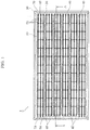
- FIG. 1 is a plan view of the solar cell module according to the embodiment.
- FIG. 2 is a partially enlarged sectional view of the solar cell module along line A-A in FIG. 1 .
- solar cell module 1 includes substrate 10, back sheet 20, plurality of solar cells 30, transition wire 40, concealment sheet 50, and filling member 60.
- Solar cell module 1 in this embodiment further includes frame 70.
- Solar cell module 1 has a structure in which solar cells 30 are sealed with filling member 60 between substrate 10 and back sheet 20 that face each other.
- solar cell module 1 is, for example, rectangular in planar view. As an example, solar cell module 1 is a rectangle of about 1600 mm in horizontal length and about 800 mm in vertical length. The shape of solar cell module 1 is not limited to a rectangle.
- Substrate 10 is a light-transmitting substrate, and is, for example, a glass substrate (transparent glass substrate) made of a transparent glass material.
- Substrate 10 is not limited to a glass substrate, and may be, for example, a resin substrate made of a light-transmitting resin material such as a transparent resin material.
- Substrate 10 is a front surface protection member for protecting the front surface of solar cell module 1, and protects the inside of solar cell module 1 from the external environment such as the wind and rain, external impact, and fire.
- substrate 10 is located on the light receiving surface side of solar cells 30, and sunlight enters from the substrate 10 side.
- the surface (exposed surface) of substrate 10 is thus the light receiving surface.
- An antireflection coating may be formed on the surface of substrate 10, to make substrate 10 a low-reflection substrate.
- Back sheet 20 is a back surface protection member for protecting the back surface of solar cell module 1, and protects the inside of solar cell module 1 from the external environment.
- Back sheet 20 is, for example, a resin sheet made of polyethylene terephthalate (PET) or polyethylene naphthalate (PEN).
- the color of back sheet 20 is black.
- the color of back sheet 20 may be, however, other than black.
- Back sheet 20 is not limited to be made of resin, and may be made of glass.
- Solar cell 30 is a photoelectric conversion element (photovoltaic element) for converting light such as sunlight into electricity. As illustrated in FIG. 1 , plurality of solar cells 30 are arranged in a matrix on the same plane to form a cell array. As illustrated in FIG. 2 , plurality of solar cells 30 (cell array) are arranged between substrate 10 and back sheet 20.
- Plurality of solar cells 30 arranged in one of the row direction and column direction are made into a cell string (solar cell group) by electrically connecting adjacent solar cells 30 by conductive tab wire (interconnector) 31.
- Plurality of solar cells 30 in the cell string are connected in series.
- Tab wire 31 may be, for example, made by cutting metal foil, such as copper foil or silver foil, the entire surface of which is coated with solder, in strip form with a predetermined length.
- plurality of solar cells 30 arranged in the row direction are connected by tab wire 31 to form a cell string.
- the respective electrodes of adjacent solar cells 30 are connected in sequence by three tab wires 31 through solder or the like, thus creating a cell string in which plurality of solar cells 30 are connected in a line.
- each solar cell 30 is connected with three tab wires 31, and twelve solar cells 30 are connected along the row direction to constitute one cell string. Six cell strings are formed in FIG. 1 .
- Transition wire 40 is horizontal wiring common-connecting tab wires 31 connected to plurality of solar cells 30.
- Transition wire 40 may be, for example, made by cutting metal foil, such as copper foil or silver foil, the entire surface of which is coated with solder, in strip form with a predetermined length.
- transition wire 40 is provided at both ends of solar cell module 1 in the longitudinal direction.
- four transition wires 40 are provided at one end (left end in FIG. 1 ) of solar cell module 1 in the longitudinal direction, and three transition wires 40 are provided at the other end (right end in FIG. 1 ) of solar cell module 1 opposite to the one end in the longitudinal direction.
- the first solar cell 30 in each cell string is electrically connected to transition wires 40 via tab wires 31, in the vicinity of the one end of solar cell module 1 in the longitudinal direction.
- the last solar cell 30 in each cell string is electrically connected to transition wires 40 via tab wires 31, in the vicinity of the other end of solar cell module 1 in the longitudinal direction.
- the plurality of (six in FIG. 1 ) cell strings are connected in series or in parallel to constitute the cell array.
- all solar cells 30 in solar cell module 1 are connected in series or in parallel.
- Concealment sheet 50 covers transition wires 40 from the substrate 10 side, in order to conceal transition wires 40. Hence, concealment sheet 50 overlaps transition wires 40 and is greater in size than transition wires 40 in planar view, as illustrated in FIG. 1 .
- transition wires 40 are provided at both ends of solar cell module 1 in the longitudinal direction, i.e. at two locations that are the one end and other end in the longitudinal direction.
- Concealment sheet 50 is accordingly provided at both ends of solar cell module 1 in the longitudinal direction.
- concealment sheet 50 provided at the one end (left end in FIG. 1 ) of solar cell module 1 in the longitudinal direction covers all (four in FIG. 1 ) transition wires 40 located at the one end together.
- Concealment sheet 50 provided at the other end (right end in FIG. 1 ) of solar cell module 1 in the longitudinal direction covers all (three in FIG. 1 ) transition wires 40 located at the other end together.
- concealment sheet 50 has a stack structure of a plurality of layers, and includes: first sheet layer 51a in contact with filling member 60; and second sheet layer 51b placed over first sheet layer 51a.
- Concealment sheet 50 in this embodiment further includes third sheet layer 51c placed over second sheet layer 51b.
- Concealment sheet 50 thus has a stack structure of three sheet layers.
- first sheet layer 51a and third sheet layer 51c each have a layer thickness of 30 pm
- second sheet layer 51b has a layer thickness of 50 ⁇ m.
- First sheet layer 51a and second sheet layer 51b are made of any of: a material of the same type of color as the material of back sheet 20 or filling member 60 (back sheet side filling member 61); a transparent material; and a semitransparent material.
- first sheet layer 51a is made of a transparent material.
- Second sheet layer 51b is made of a material of the same type of color as the material of back sheet 20 or filling member 60 (back sheet side filling member 61), and is made of a black material to match the color of back sheet 20 in this embodiment.
- Third sheet layer 51c is made of the same material (transparent material) as first sheet layer 51.
- first sheet layer 51a is a resin sheet (PE sheet) made of polyethylene (PE)
- second sheet layer 51b is a resin sheet (PET sheet) made of polyethylene terephthalate (PET).
- Third sheet layer 51c is made of the same material as first sheet layer 51a, and is a resin sheet (PE sheet) made of polyethylene (PE) in this embodiment.
- First sheet layer 51a has adhesiveness to filling member 60. This enables first sheet layer 51a and filling member 60 to adhere to each other, without interposing an additional adhesive in between.
- first sheet layer 51a has adhesiveness to filling member 60 filling the space between transition wires 40 and concealment sheet 50.
- first sheet layer 51a is in contact with back sheet side filling member 61, and has adhesiveness to back sheet side filling member 61. This enables first sheet layer 51a and back sheet side filling member 61 to adhere to each other without using an adhesive.
- PE polyethylene
- EVA ethylene vinyl acetate
- Third sheet layer 51c also has adhesiveness to filling member 60. This enables third sheet layer 51c and filling member 60 to adhere to each other, without interposing an additional adhesive in between.
- third sheet layer 51c has adhesiveness to filling member 60 filling the space between substrate 10 and concealment sheet 50.
- third sheet layer 51c is in contact with substrate side filling member 62, and has adhesiveness to substrate side filling member 62. This enables third sheet layer 51c and substrate side filling member 62 to adhere to each other without using an adhesive.
- PE Polyethylene
- EVA ethylene vinyl acetate
- first sheet layer 51a and third sheet layer 51c adhere to and merge with filling member 60 after a lamination process.
- the material of second sheet layer 51b is PET.
- PET This realizes concealment sheet 50 having favorable long-term reliability and necessary strength (stiffness) in appearance.
- the use of PET as the material of second sheet layer 51b also facilitates operation in the manufacturing process.
- substrate 10 glass
- substrate side filling member 62 substrate side filling member 62
- transition wires 40 are stacked in this order, and concealment sheet 50 is inserted between substrate side filling member 62 and transition wires 40.
- transition wires 40 are lifted with tweezers, and concealment sheet 50 is inserted into the gap between transition wires 40 and substrate side filling member 62.
- the use of PET with relatively high strength as the material of second sheet layer 51b facilitates the operation of inserting concealment sheet 50.
- Concealment sheet 50 further includes: first adhesion layer 52a for causing first sheet layer 51a and second sheet layer 51b to adhere to each other; and second adhesion layer 52b for causing second sheet layer 51b and third sheet layer 51c to adhere to each other.
- Inserting first adhesion layer 52a between first sheet layer 51a and second sheet layer 51b eases the adhesion between first sheet layer 51a and second sheet layer 51b.
- Inserting second adhesion layer 52b between second sheet layer 51b and third sheet layer 51c eases the adhesion between second sheet layer 51b and third sheet layer 51c.
- first adhesion layer 52a and second adhesion layer 52b is black to match the color of back sheet 20.
- Concealment sheet 50 having the aforementioned structure can be produced in the following manner. For example, a structure obtained by bonding three plate-like sheet layers of plate-like first sheet layer 51a, plate-like second sheet layer 51b, and plate-like third sheet layer 51c by adhesion with two adhesion layers of first adhesion layer 52a and second adhesion layer 52b is cut in strip form with a predetermined length. Since concealment sheet 50 in this embodiment covers plurality of transition wires 40 located at each of both ends of solar cell module 1 in the longitudinal direction together, the length of concealment sheet 50 is approximately the length of the short side of solar cell module 1.
- Filling member (filler) 60 is located between substrate 10 and back sheet 20. In this embodiment, filling member 60 fills the space between substrate 10 and back sheet 20. Solar cells 30 are thus sealed with filling member 60.
- Filling member 60 is formed by performing a lamination process (lamination) on the two filling members sandwiching solar cells 30.
- the lamination process is described below, with reference to FIG. 3.
- FIG. 3 is a view for describing the lamination process in the solar cell module according to the embodiment.
- the plurality of cell strings composed of plurality of solar cells 30 are sandwiched between back sheet side filling member 61 and substrate side filling member 62, and back sheet 20 and substrate 10 are placed below and above the sandwich structure, to prepare a predetermined stack body.
- the stack body is then subjected to thermocompression bonding (heating and pressing) in a vacuum at a temperature of 100°C or higher as an example.
- thermocompression bonding heating and pressing
- back sheet side filling member 61 and substrate side filling member 62 are heated to melt, and form filling member 60.
- the space between substrate 10 and back sheet 20 is filled with filling member 60, and solar cells 30, transition wires 40, and concealment sheet 50 are sealed with filling member 60.
- Back sheet side filling member (first filling member) 61 is a sheet located between back sheet 20 and each of: plurality of solar cells 30; and transition wires 40, and mainly fills the space between back sheet 20 and transition wires 40 and solar cells 30 as a result of the lamination process.
- Substrate side filling member (second filling member) 62 is a sheet located between substrate 10 and each of: plurality of solar cells 30; and concealment sheet 50, and mainly fills the space between substrate 10 and solar cells 30 and concealment sheet 50 as a result of the lamination process.
- Each of back sheet side filling member 61 and substrate side filling member 62 is, for example, a resin sheet made of a resin material, and is an EVA sheet made of ethylene vinyl acetate (EVA) in this embodiment.
- EVA ethylene vinyl acetate
- the color of back sheet side filling member 61 and substrate side filling member 62 is, for example, black.
- the color of filling member 60 is therefore black.
- Frame 70 is an outer frame covering the peripheral edges of solar cell module 1.
- Frame 70 in this embodiment is an aluminum frame made of aluminum. As illustrated in FIG. 1 , four frames 70 are attached to the respective edges of the four sides of solar cell module 1.
- frame 70 is bonded to the edge of each side of solar cell module 1 by adhesive 71 made of silicone resin.
- the solar cell module is provided with a terminal box for extracting power generated in solar cells 30, although not illustrated.
- the terminal box is fixed to back sheet 20, and contains a plurality of circuit components mounted on a circuit substrate.
- FIGS. 4A and 4B are sectional views illustrating the structure of a solar cell module according to the comparative example.
- FIG. 4A illustrates the structure before the lamination process
- FIG. 4B illustrates the structure after the lamination process.
- the first and last solar cells in each cell string are connected to the transition wires via the tab wires.
- the transition wires have metallic luster, and so are noticeable in the case where the solar cell module is seen from the glass substrate side. This causes poor design of the solar cell module as a whole.
- the present inventors studied covering transition wires 40 with concealment sheet 500 from the substrate 10 side (light receiving surface side) to conceal transition wires 40, as illustrated in FIGS. 4A and 4B .
- Concealment sheet 500 studied here had a structure in which stack PET composed of first sheet layer 510a (38 ⁇ m) made of PET and second sheet layer 510b (50 ⁇ m) made of PET was caused to adhere to third sheet layer 510c made of PE by adhesion layer 520.
- First sheet layer 510a and second sheet layer 510b were white, third sheet layer 510c was transparent, and adhesion layer 520 was black.
- concealment sheet 500 was thus studied in order to improve design.
- providing concealment sheet 500 ended up rather degrading design. This is described in detail below.
- first sheet layer 510a second sheet layer 510b, adhesion layer 520, and third sheet layer 510c in concealment sheet 500 were selected as mentioned above, for color matching with back sheet 20 and the like.
- concealment sheet 500 was formed by cutting the stacked sheet layers to a predetermined length, in the case where the cutting state was poor, the edges of first sheet layer 510a and white second sheet layer 510b protruded (were exposed), making white lines very visible.
- the present inventors found out as a result of the study that placing concealment sheet 500 having the aforementioned structure rather degraded design.
- the present inventors also found out that the use of concealment sheet 500 having the aforementioned structure caused lower workability and higher cost. This is described in detail below.
- concealment filling member 63 needed to be placed between concealment sheet 500 and transition wires 40.
- concealment sheet 500 needed to adhere to transition wires 40 through concealment filling member 63.
- Concealment filling member 63 was, for example, made of the same material (EVA sheet) as back sheet side filling member 61 and substrate side filling member 62.
- the present invention was made based on such findings. As a result of keen examination, the present inventors discovered that the use of concealment sheet 50 having the structure illustrated in FIG. 2 can conceal transition wires 40 without degrading design and workability.
- concealment sheet 50 used in solar cell module 1 in this embodiment includes: first sheet layer 51a in contact with at least filling member 60; and second sheet layer 51b placed over first sheet layer 51a.
- First sheet layer 51a and second sheet layer 51b are made of any of: a material of the same type of color as the material of back sheet 20 or filling member 60; a transparent material; and a semitransparent material.
- concealment sheet 50 is not noticeable even in the case where the edges of first sheet layer 51a and second sheet layer 51b protrude from concealment sheet 50 due to a poor cutting state of concealment sheet 50.
- transition wires 40 can be concealed by concealment sheet 50, but also concealment sheet 50 can be made unnoticeable regardless of the cutting state of concealment sheet 50. This improves the design of the whole appearance of solar cell module 1.
- first sheet layer 51a has adhesiveness to filling member 60, and so concealment filling member 63 in the comparative example in FIG. 4A can be substituted by first sheet layer 51a.
- first sheet layer 51a in this embodiment is made of polyethylene (PE)
- concealment filling member 63 made of EVA can be easily substituted by first sheet layer 51a made of PE.
- Concealment sheet 50 can thus adhere to filling member 60 without using concealment filling member 63. This prevents an increase in the number of parts, and therefore prevents lower workability and higher cost.
- solar cell module 1 can conceal transition wires 40 without degrading design and workability.
- first sheet layer 51a is made of the transparent material or the semitransparent material
- second sheet layer 51b has the same type of color as back sheet 20 or filling member 60.
- back sheet 20 or filling member 60 is black
- second sheet layer 51b is black, too.
- concealment sheet 50 has no white layer. This avoids such a situation where, due to the black background color of back sheet 20 or filling member 60, white lines of the concealment sheet are visible in the case where the concealment sheet has a white layer.
- concealment sheet 50 further includes third sheet layer 51c placed over second sheet layer 51b, and third sheet layer 51c is made of the same material as first sheet layer 51a.
- transition wires 40 can be concealed without degrading design and workability, even in the case where concealment sheet 50 further includes third sheet layer 51c.
- substrate side filling member 62 fills the space between concealment sheet 50 and substrate 10, and third sheet layer 51c is in contact with substrate side filling member 62 and has adhesiveness to substrate side filling member 62.
- concealment sheet 50 may have no black layer in the case where back sheet 20 and filling member 60 are white.
Landscapes
- Photovoltaic Devices (AREA)
- Health & Medical Sciences (AREA)
- Life Sciences & Earth Sciences (AREA)
- Molecular Biology (AREA)
- Sustainable Development (AREA)
Claims (11)
- Solarzellenmodul (1) umfassend:ein lichtübertragendes bzw. lichtdurchlässiges Substrat (10);eine hintere Lage (20);eine Mehrzahl von Solarzellen (30), die zwischen dem Substrat (10) und der hinteren Lage (20) angeordnet sind;einen Übergangsdraht (40), der Kopplungs- bzw. Verbindungsdrähte miteinander verbindet, wobei die Kopplungs- bzw. Verbindungsdrähte mit der Mehrzahl von Solarzellen (30) verbunden sind;eine Verdeckungslage (50), die den Übergangsdraht (40) von einer Substratseite aus verdeckt; undein Füllglied (60), das einen Raum zwischen dem Substrat (10) und der hinteren Lage (20) füllt, umfassend ein substratseitiges Füllglied (62), das einen Raum zwischen der Verdeckungslage (50) und dem Substrat (10) füllt,wobei der Übergangsdraht (40) in dem Füllglied (60) angeordnet ist,wobei die Verdeckungslage (50) enthält: eine erste Lagenschicht (51a) in Kontakt mit dem Füllglied (60); eine zweite Lagenschicht (51b), die über der ersten Lagenschicht (51a) auf der Substratseite platziert ist; und eine dritte Lagenschicht (51c), die über der zweiten Lagenschicht (51b) auf der Substratseite platziert ist,wobei die erste Lagenschicht (51a) aus einem transparenten Material oder einem semitransparenten Material besteht,wobei die zweite Lagenschicht (51b) aus einem Material der gleichen Art von Farbe wie ein Material hinteren Lage (20) oder des Füllglieds (60) besteht,wobei die erste Lagenschicht (51a) an dem Füllglied (60) haftet, undwobei die dritte Lagenschicht (51c) mit dem substratseitigen Füllglied (62) in Kontakt ist und an dem substratseitigen Füllglied (62) haftet.
- Solarzellenmodul (1) nach Anspruch 1,
wobei die hintere Lage (20) oder das Füllglied (60) schwarz ist, und
die zweite Lagenschicht (51b) schwarz ist. - Solarzellenmodul nach Anspruch 2,
wobei die Verdeckungslage (50) ferner eine erste Haftschicht (52a) enthält, die bewirkt, dass die erste Lagenschicht (51a) und die zweite Lagenschicht (51b) aneinander haften, und
die erste Haftschicht (52a) schwarz ist. - Solarzellenmodul (1) nach Anspruch 3,
wobei die Verdeckungslage (50) ferner enthält: eine zweite Haftschicht (52b), die bewirkt, dass die zweite Lagenschicht (51b) und die dritte Lagenschicht (51c) aneinander haften. - Solarzellenmodul nach Anspruch 4,
wobei die dritte Lagenschicht aus dem gleichen Material wie die erste Lagenschicht (51a) besteht. - Solarzellenmodul (1) nach einem der Ansprüche 1 bis 5;
wobei die erste Lagenschicht (51a) aus Polyethylen besteht,
die zweite Lagenschicht (51b) aus Polyethylenterephthalat besteht, und
das Füllglied (60) aus Ethylenvinylacetat besteht. - Verfahren zum Herstellen eines Solarzellenmoduls (1) nach Anspruch 1, das ein lichtübertragendes bzw. lichtdurchlässiges Substrat (10) und eine hinteren Lage (20) enthält, wobei das Verfahren umfasst:Anordnen, zwischen dem Substrat (10) und der hinteren Lage (20): eine Mehrzahl von Solarzellen (30); einen Übergangsdraht (40), der Kopplungs- bzw. Verbindungsdrähte miteinander verbindet, wobei die Kopplungs- bzw. Verbindungsdrähte mit der Mehrzahl von Solarzellen (30) verbunden sind; eine Verdeckungslage (50), die den Übergangsdraht (40) von einer Substratseite aus bedeckt; und ein Füllglied (60), das einen Raum zwischen dem Substrat (10) und der hinteren Lage (20) füllt, umfassend ein substratseitiges Füllglied (62), das einen Raum zwischen der Verdeckungslage (50) und dem Substrat (10) füllt,wobei die Verdeckungslage (50) enthält: eine erste Lagenschicht (51a) in Kontakt mit dem Füllglied; und eine zweite Lagenschicht (51b), die über der ersten Lagenschicht (51a) auf der Substratseite platziert ist; und eine dritte Lagenschicht (51c), die über der zweiten Lagenschicht (51b) auf der Substratseite platziert ist,wobei die erste Lagenschicht (51a) aus einem transparenten Material oder einem semitransparenten Material besteht, die zweite Lagenschicht (51b) aus einem Material der gleichen Art von Farbe wie ein Material hinteren Lage (20) oder des Füllglieds (60) besteht, die erste Lagenschicht (51a) an dem Füllglied (60) haftet, und die dritte Lagenschicht (51c) mit dem substratseitigen Füllglied (62) in Kontakt ist und an dem substratseitigen Füllglied (62) haftet.
- Verfahren zum Herstellen des Solarzellenmoduls (1) nach Anspruch 7, wobei das Verfahren ferner umfasst:Erwärmen und Pressen, in einem Vakuum, des Stapelkörpers, der durch den Schritt des Anordnens der Mehrzahl von Solarzellen (30), des Übergangsdrahtes (40), der Verdeckungslage (40) und des Füllglieds (60) zwischen dem Substrat (10) und der hinteren Lage (20) hergestellt wird.
- Verfahren zum Herstellen des Solarzellenmoduls (1) nach einem der Ansprüche 7 oder 8,
wobei die hintere Lage (20) oder das Füllglied (60) schwarz ist, und
die zweite Lagenschicht (51b) schwarz ist. - Verfahren zum Herstellen des Solarzellenmoduls (1) nach Anspruch 9,
wobei die Verdeckungslage (50) ferner eine erste Haftschicht (52a) enthält, die bewirkt, dass die erste Lagenschicht (51a) und die zweite Lagenschicht (51b) aneinander haften, und
die erste Haftschicht (52a) schwarz ist. - Verfahren zum Herstellen des Solarzellenmoduls (1) nach einem der Ansprüche 7 bis 10;
wobei die erste Lagenschicht (51a) und die dritte Lagenschicht (51c) aus Polyethylen bestehen,
die zweite Lagenschicht (51b) aus Polyethylenterephthalat besteht, und das Füllglied (60) aus Ethylenvinylacetat besteht.
Applications Claiming Priority (2)
| Application Number | Priority Date | Filing Date | Title |
|---|---|---|---|
| JP2014192732 | 2014-09-22 | ||
| PCT/JP2015/004167 WO2016047029A1 (ja) | 2014-09-22 | 2015-08-20 | 太陽電池モジュール及び太陽電池モジュールの製造方法 |
Publications (3)
| Publication Number | Publication Date |
|---|---|
| EP3200239A1 EP3200239A1 (de) | 2017-08-02 |
| EP3200239A4 EP3200239A4 (de) | 2017-09-20 |
| EP3200239B1 true EP3200239B1 (de) | 2021-04-14 |
Family
ID=55580583
Family Applications (1)
| Application Number | Title | Priority Date | Filing Date |
|---|---|---|---|
| EP15844110.5A Active EP3200239B1 (de) | 2014-09-22 | 2015-08-20 | Solarzellenmodul und verfahren zur herstellung des solarzellenmoduls |
Country Status (4)
| Country | Link |
|---|---|
| US (1) | US20170278992A1 (de) |
| EP (1) | EP3200239B1 (de) |
| JP (1) | JP6587191B2 (de) |
| WO (1) | WO2016047029A1 (de) |
Families Citing this family (2)
| Publication number | Priority date | Publication date | Assignee | Title |
|---|---|---|---|---|
| CN110216948B (zh) * | 2019-05-31 | 2022-02-08 | 保定嘉盛光电科技股份有限公司 | 一种瓦片双玻组件生产工艺 |
| TWI888529B (zh) * | 2020-04-09 | 2025-07-01 | 日商鐘化股份有限公司 | 太陽電池模組 |
Family Cites Families (10)
| Publication number | Priority date | Publication date | Assignee | Title |
|---|---|---|---|---|
| US7390961B2 (en) * | 2004-06-04 | 2008-06-24 | Sunpower Corporation | Interconnection of solar cells in a solar cell module |
| JP4860652B2 (ja) * | 2008-03-31 | 2012-01-25 | 京セラ株式会社 | 太陽電池モジュールおよびその製造方法 |
| US20110036390A1 (en) * | 2009-08-11 | 2011-02-17 | Miasole | Composite encapsulants containing fillers for photovoltaic modules |
| JP2011054663A (ja) * | 2009-08-31 | 2011-03-17 | Sanyo Electric Co Ltd | 太陽電池モジュール |
| JP5676944B2 (ja) * | 2010-07-08 | 2015-02-25 | デクセリアルズ株式会社 | 太陽電池モジュール、太陽電池モジュールの製造方法 |
| JP2012033546A (ja) * | 2010-07-28 | 2012-02-16 | Sharp Corp | 太陽電池モジュール |
| CN102646740B (zh) * | 2011-02-18 | 2015-06-10 | 3M创新有限公司 | 胶带及由其制成的太阳能组件和制品 |
| CN102623533B (zh) * | 2012-03-16 | 2014-07-23 | 友达光电股份有限公司 | 可吸收紫外光波段的太阳能模块及其制作方法 |
| JP6104612B2 (ja) * | 2013-01-16 | 2017-03-29 | シャープ株式会社 | 太陽電池モジュール |
| CN104508832A (zh) * | 2012-08-22 | 2015-04-08 | 三洋电机株式会社 | 太阳能电池组件和其制造方法 |
-
2015
- 2015-08-20 US US15/512,066 patent/US20170278992A1/en not_active Abandoned
- 2015-08-20 EP EP15844110.5A patent/EP3200239B1/de active Active
- 2015-08-20 WO PCT/JP2015/004167 patent/WO2016047029A1/ja not_active Ceased
- 2015-08-20 JP JP2016549907A patent/JP6587191B2/ja active Active
Non-Patent Citations (1)
| Title |
|---|
| None * |
Also Published As
| Publication number | Publication date |
|---|---|
| EP3200239A1 (de) | 2017-08-02 |
| JP6587191B2 (ja) | 2019-10-09 |
| US20170278992A1 (en) | 2017-09-28 |
| EP3200239A4 (de) | 2017-09-20 |
| JPWO2016047029A1 (ja) | 2017-06-29 |
| WO2016047029A1 (ja) | 2016-03-31 |
Similar Documents
| Publication | Publication Date | Title |
|---|---|---|
| TWI413266B (zh) | 太陽能電池模組 | |
| JP4860652B2 (ja) | 太陽電池モジュールおよびその製造方法 | |
| US8609983B2 (en) | Interconnection sheet, solar cell with interconnection sheet, solar cell module, and interconnection sheet roll | |
| US8461450B2 (en) | Solar cell module and manufacturing method of solar cell module | |
| JP5879513B2 (ja) | 太陽電池モジュール | |
| JP5164863B2 (ja) | 太陽電池用配線部材、太陽電池モジュール、および太陽電池モジュールの製造方法 | |
| TW201349529A (zh) | 背接觸型太陽能電池模組 | |
| JP2011054663A (ja) | 太陽電池モジュール | |
| KR101605132B1 (ko) | 태양 전지 모듈 및 그 제조 방법 | |
| JP2019102620A (ja) | 太陽電池モジュール | |
| WO2011024991A1 (ja) | 太陽電池モジュール | |
| WO2013183395A1 (ja) | 太陽電池モジュール及び太陽電池モジュールの製造方法 | |
| JP5089548B2 (ja) | 太陽電池モジュールおよび太陽電池モジュールの製造方法 | |
| JP5637089B2 (ja) | 太陽電池モジュール | |
| JP2005191125A (ja) | 太陽電池素子接続用接続タブ及び太陽電池モジュール並びに太陽電池モジュールの製造方法 | |
| JP2011054662A (ja) | 太陽電池モジュール | |
| EP3200239B1 (de) | Solarzellenmodul und verfahren zur herstellung des solarzellenmoduls | |
| CN204760395U (zh) | 可挠式太阳能板模块及其固定结构 | |
| US9373738B2 (en) | Solar module | |
| JP3605998B2 (ja) | 太陽電池モジュールとその製造方法 | |
| US20150228828A1 (en) | Solar cell module and method of fabricating the same | |
| JP2012204533A (ja) | 太陽電池モジュール及びその製造方法 | |
| JP2014013838A (ja) | 太陽電池用集電シート及び太陽電池モジュール | |
| JP5312284B2 (ja) | 太陽電池モジュール及びその製造方法 | |
| JP6042710B2 (ja) | 太陽電池モジュール、及び太陽電池モジュールの製造方法 |
Legal Events
| Date | Code | Title | Description |
|---|---|---|---|
| STAA | Information on the status of an ep patent application or granted ep patent |
Free format text: STATUS: THE INTERNATIONAL PUBLICATION HAS BEEN MADE |
|
| PUAI | Public reference made under article 153(3) epc to a published international application that has entered the european phase |
Free format text: ORIGINAL CODE: 0009012 |
|
| STAA | Information on the status of an ep patent application or granted ep patent |
Free format text: STATUS: REQUEST FOR EXAMINATION WAS MADE |
|
| 17P | Request for examination filed |
Effective date: 20170316 |
|
| AK | Designated contracting states |
Kind code of ref document: A1 Designated state(s): AL AT BE BG CH CY CZ DE DK EE ES FI FR GB GR HR HU IE IS IT LI LT LU LV MC MK MT NL NO PL PT RO RS SE SI SK SM TR |
|
| AX | Request for extension of the european patent |
Extension state: BA ME |
|
| A4 | Supplementary search report drawn up and despatched |
Effective date: 20170822 |
|
| RIC1 | Information provided on ipc code assigned before grant |
Ipc: H01L 31/048 20140101AFI20170816BHEP Ipc: H01L 31/05 20140101ALI20170816BHEP |
|
| DAV | Request for validation of the european patent (deleted) | ||
| DAX | Request for extension of the european patent (deleted) | ||
| STAA | Information on the status of an ep patent application or granted ep patent |
Free format text: STATUS: EXAMINATION IS IN PROGRESS |
|
| 17Q | First examination report despatched |
Effective date: 20191111 |
|
| GRAP | Despatch of communication of intention to grant a patent |
Free format text: ORIGINAL CODE: EPIDOSNIGR1 |
|
| STAA | Information on the status of an ep patent application or granted ep patent |
Free format text: STATUS: GRANT OF PATENT IS INTENDED |
|
| INTG | Intention to grant announced |
Effective date: 20201116 |
|
| GRAS | Grant fee paid |
Free format text: ORIGINAL CODE: EPIDOSNIGR3 |
|
| GRAA | (expected) grant |
Free format text: ORIGINAL CODE: 0009210 |
|
| STAA | Information on the status of an ep patent application or granted ep patent |
Free format text: STATUS: THE PATENT HAS BEEN GRANTED |
|
| RIN1 | Information on inventor provided before grant (corrected) |
Inventor name: ICHINOSE, HITOMI Inventor name: NAKAMURA, TAKAHIRO Inventor name: KOUYANAGI, MASAO Inventor name: YAMASHITA, MAMORU |
|
| AK | Designated contracting states |
Kind code of ref document: B1 Designated state(s): AL AT BE BG CH CY CZ DE DK EE ES FI FR GB GR HR HU IE IS IT LI LT LU LV MC MK MT NL NO PL PT RO RS SE SI SK SM TR |
|
| REG | Reference to a national code |
Ref country code: GB Ref legal event code: FG4D |
|
| REG | Reference to a national code |
Ref country code: CH Ref legal event code: EP |
|
| REG | Reference to a national code |
Ref country code: DE Ref legal event code: R096 Ref document number: 602015068213 Country of ref document: DE |
|
| REG | Reference to a national code |
Ref country code: IE Ref legal event code: FG4D |
|
| REG | Reference to a national code |
Ref country code: AT Ref legal event code: REF Ref document number: 1383227 Country of ref document: AT Kind code of ref document: T Effective date: 20210515 |
|
| REG | Reference to a national code |
Ref country code: LT Ref legal event code: MG9D |
|
| REG | Reference to a national code |
Ref country code: AT Ref legal event code: MK05 Ref document number: 1383227 Country of ref document: AT Kind code of ref document: T Effective date: 20210414 |
|
| REG | Reference to a national code |
Ref country code: NL Ref legal event code: MP Effective date: 20210414 |
|
| PG25 | Lapsed in a contracting state [announced via postgrant information from national office to epo] |
Ref country code: NL Free format text: LAPSE BECAUSE OF FAILURE TO SUBMIT A TRANSLATION OF THE DESCRIPTION OR TO PAY THE FEE WITHIN THE PRESCRIBED TIME-LIMIT Effective date: 20210414 Ref country code: LT Free format text: LAPSE BECAUSE OF FAILURE TO SUBMIT A TRANSLATION OF THE DESCRIPTION OR TO PAY THE FEE WITHIN THE PRESCRIBED TIME-LIMIT Effective date: 20210414 Ref country code: FI Free format text: LAPSE BECAUSE OF FAILURE TO SUBMIT A TRANSLATION OF THE DESCRIPTION OR TO PAY THE FEE WITHIN THE PRESCRIBED TIME-LIMIT Effective date: 20210414 Ref country code: HR Free format text: LAPSE BECAUSE OF FAILURE TO SUBMIT A TRANSLATION OF THE DESCRIPTION OR TO PAY THE FEE WITHIN THE PRESCRIBED TIME-LIMIT Effective date: 20210414 Ref country code: AT Free format text: LAPSE BECAUSE OF FAILURE TO SUBMIT A TRANSLATION OF THE DESCRIPTION OR TO PAY THE FEE WITHIN THE PRESCRIBED TIME-LIMIT Effective date: 20210414 Ref country code: BG Free format text: LAPSE BECAUSE OF FAILURE TO SUBMIT A TRANSLATION OF THE DESCRIPTION OR TO PAY THE FEE WITHIN THE PRESCRIBED TIME-LIMIT Effective date: 20210714 |
|
| PG25 | Lapsed in a contracting state [announced via postgrant information from national office to epo] |
Ref country code: LV Free format text: LAPSE BECAUSE OF FAILURE TO SUBMIT A TRANSLATION OF THE DESCRIPTION OR TO PAY THE FEE WITHIN THE PRESCRIBED TIME-LIMIT Effective date: 20210414 Ref country code: IS Free format text: LAPSE BECAUSE OF FAILURE TO SUBMIT A TRANSLATION OF THE DESCRIPTION OR TO PAY THE FEE WITHIN THE PRESCRIBED TIME-LIMIT Effective date: 20210814 Ref country code: GR Free format text: LAPSE BECAUSE OF FAILURE TO SUBMIT A TRANSLATION OF THE DESCRIPTION OR TO PAY THE FEE WITHIN THE PRESCRIBED TIME-LIMIT Effective date: 20210715 Ref country code: NO Free format text: LAPSE BECAUSE OF FAILURE TO SUBMIT A TRANSLATION OF THE DESCRIPTION OR TO PAY THE FEE WITHIN THE PRESCRIBED TIME-LIMIT Effective date: 20210714 Ref country code: PL Free format text: LAPSE BECAUSE OF FAILURE TO SUBMIT A TRANSLATION OF THE DESCRIPTION OR TO PAY THE FEE WITHIN THE PRESCRIBED TIME-LIMIT Effective date: 20210414 Ref country code: PT Free format text: LAPSE BECAUSE OF FAILURE TO SUBMIT A TRANSLATION OF THE DESCRIPTION OR TO PAY THE FEE WITHIN THE PRESCRIBED TIME-LIMIT Effective date: 20210816 Ref country code: SE Free format text: LAPSE BECAUSE OF FAILURE TO SUBMIT A TRANSLATION OF THE DESCRIPTION OR TO PAY THE FEE WITHIN THE PRESCRIBED TIME-LIMIT Effective date: 20210414 Ref country code: RS Free format text: LAPSE BECAUSE OF FAILURE TO SUBMIT A TRANSLATION OF THE DESCRIPTION OR TO PAY THE FEE WITHIN THE PRESCRIBED TIME-LIMIT Effective date: 20210414 |
|
| REG | Reference to a national code |
Ref country code: DE Ref legal event code: R097 Ref document number: 602015068213 Country of ref document: DE |
|
| PG25 | Lapsed in a contracting state [announced via postgrant information from national office to epo] |
Ref country code: ES Free format text: LAPSE BECAUSE OF FAILURE TO SUBMIT A TRANSLATION OF THE DESCRIPTION OR TO PAY THE FEE WITHIN THE PRESCRIBED TIME-LIMIT Effective date: 20210414 Ref country code: RO Free format text: LAPSE BECAUSE OF FAILURE TO SUBMIT A TRANSLATION OF THE DESCRIPTION OR TO PAY THE FEE WITHIN THE PRESCRIBED TIME-LIMIT Effective date: 20210414 Ref country code: SK Free format text: LAPSE BECAUSE OF FAILURE TO SUBMIT A TRANSLATION OF THE DESCRIPTION OR TO PAY THE FEE WITHIN THE PRESCRIBED TIME-LIMIT Effective date: 20210414 Ref country code: SM Free format text: LAPSE BECAUSE OF FAILURE TO SUBMIT A TRANSLATION OF THE DESCRIPTION OR TO PAY THE FEE WITHIN THE PRESCRIBED TIME-LIMIT Effective date: 20210414 Ref country code: EE Free format text: LAPSE BECAUSE OF FAILURE TO SUBMIT A TRANSLATION OF THE DESCRIPTION OR TO PAY THE FEE WITHIN THE PRESCRIBED TIME-LIMIT Effective date: 20210414 Ref country code: CZ Free format text: LAPSE BECAUSE OF FAILURE TO SUBMIT A TRANSLATION OF THE DESCRIPTION OR TO PAY THE FEE WITHIN THE PRESCRIBED TIME-LIMIT Effective date: 20210414 Ref country code: DK Free format text: LAPSE BECAUSE OF FAILURE TO SUBMIT A TRANSLATION OF THE DESCRIPTION OR TO PAY THE FEE WITHIN THE PRESCRIBED TIME-LIMIT Effective date: 20210414 |
|
| PLBE | No opposition filed within time limit |
Free format text: ORIGINAL CODE: 0009261 |
|
| STAA | Information on the status of an ep patent application or granted ep patent |
Free format text: STATUS: NO OPPOSITION FILED WITHIN TIME LIMIT |
|
| 26N | No opposition filed |
Effective date: 20220117 |
|
| REG | Reference to a national code |
Ref country code: CH Ref legal event code: PL |
|
| PG25 | Lapsed in a contracting state [announced via postgrant information from national office to epo] |
Ref country code: MC Free format text: LAPSE BECAUSE OF FAILURE TO SUBMIT A TRANSLATION OF THE DESCRIPTION OR TO PAY THE FEE WITHIN THE PRESCRIBED TIME-LIMIT Effective date: 20210414 |
|
| REG | Reference to a national code |
Ref country code: BE Ref legal event code: MM Effective date: 20210831 |
|
| GBPC | Gb: european patent ceased through non-payment of renewal fee |
Effective date: 20210820 |
|
| PG25 | Lapsed in a contracting state [announced via postgrant information from national office to epo] |
Ref country code: CH Free format text: LAPSE BECAUSE OF NON-PAYMENT OF DUE FEES Effective date: 20210831 Ref country code: LI Free format text: LAPSE BECAUSE OF NON-PAYMENT OF DUE FEES Effective date: 20210831 |
|
| PG25 | Lapsed in a contracting state [announced via postgrant information from national office to epo] |
Ref country code: IS Free format text: LAPSE BECAUSE OF FAILURE TO SUBMIT A TRANSLATION OF THE DESCRIPTION OR TO PAY THE FEE WITHIN THE PRESCRIBED TIME-LIMIT Effective date: 20210814 Ref country code: LU Free format text: LAPSE BECAUSE OF NON-PAYMENT OF DUE FEES Effective date: 20210820 Ref country code: AL Free format text: LAPSE BECAUSE OF FAILURE TO SUBMIT A TRANSLATION OF THE DESCRIPTION OR TO PAY THE FEE WITHIN THE PRESCRIBED TIME-LIMIT Effective date: 20210414 |
|
| PG25 | Lapsed in a contracting state [announced via postgrant information from national office to epo] |
Ref country code: IT Free format text: LAPSE BECAUSE OF FAILURE TO SUBMIT A TRANSLATION OF THE DESCRIPTION OR TO PAY THE FEE WITHIN THE PRESCRIBED TIME-LIMIT Effective date: 20210414 Ref country code: IE Free format text: LAPSE BECAUSE OF NON-PAYMENT OF DUE FEES Effective date: 20210820 Ref country code: GB Free format text: LAPSE BECAUSE OF NON-PAYMENT OF DUE FEES Effective date: 20210820 Ref country code: FR Free format text: LAPSE BECAUSE OF NON-PAYMENT OF DUE FEES Effective date: 20210831 Ref country code: BE Free format text: LAPSE BECAUSE OF NON-PAYMENT OF DUE FEES Effective date: 20210831 |
|
| PG25 | Lapsed in a contracting state [announced via postgrant information from national office to epo] |
Ref country code: HU Free format text: LAPSE BECAUSE OF FAILURE TO SUBMIT A TRANSLATION OF THE DESCRIPTION OR TO PAY THE FEE WITHIN THE PRESCRIBED TIME-LIMIT; INVALID AB INITIO Effective date: 20150820 |
|
| PG25 | Lapsed in a contracting state [announced via postgrant information from national office to epo] |
Ref country code: CY Free format text: LAPSE BECAUSE OF FAILURE TO SUBMIT A TRANSLATION OF THE DESCRIPTION OR TO PAY THE FEE WITHIN THE PRESCRIBED TIME-LIMIT Effective date: 20210414 |
|
| PGFP | Annual fee paid to national office [announced via postgrant information from national office to epo] |
Ref country code: DE Payment date: 20230821 Year of fee payment: 9 |
|
| PG25 | Lapsed in a contracting state [announced via postgrant information from national office to epo] |
Ref country code: MK Free format text: LAPSE BECAUSE OF FAILURE TO SUBMIT A TRANSLATION OF THE DESCRIPTION OR TO PAY THE FEE WITHIN THE PRESCRIBED TIME-LIMIT Effective date: 20210414 |
|
| PG25 | Lapsed in a contracting state [announced via postgrant information from national office to epo] |
Ref country code: MT Free format text: LAPSE BECAUSE OF FAILURE TO SUBMIT A TRANSLATION OF THE DESCRIPTION OR TO PAY THE FEE WITHIN THE PRESCRIBED TIME-LIMIT Effective date: 20210414 |
|
| REG | Reference to a national code |
Ref country code: DE Ref legal event code: R079 Ref document number: 602015068213 Country of ref document: DE Free format text: PREVIOUS MAIN CLASS: H01L0031048000 Ipc: H10F0019800000 |
|
| REG | Reference to a national code |
Ref country code: DE Ref legal event code: R119 Ref document number: 602015068213 Country of ref document: DE |
|
| PG25 | Lapsed in a contracting state [announced via postgrant information from national office to epo] |
Ref country code: DE Free format text: LAPSE BECAUSE OF NON-PAYMENT OF DUE FEES Effective date: 20250301 |
|
| PG25 | Lapsed in a contracting state [announced via postgrant information from national office to epo] |
Ref country code: TR Free format text: LAPSE BECAUSE OF FAILURE TO SUBMIT A TRANSLATION OF THE DESCRIPTION OR TO PAY THE FEE WITHIN THE PRESCRIBED TIME-LIMIT Effective date: 20210414 |