EP3191858B1 - Distributed voltage network circuits employing voltage averaging, and related systems and methods - Google Patents
Distributed voltage network circuits employing voltage averaging, and related systems and methods Download PDFInfo
- Publication number
- EP3191858B1 EP3191858B1 EP15762830.6A EP15762830A EP3191858B1 EP 3191858 B1 EP3191858 B1 EP 3191858B1 EP 15762830 A EP15762830 A EP 15762830A EP 3191858 B1 EP3191858 B1 EP 3191858B1
- Authority
- EP
- European Patent Office
- Prior art keywords
- voltage
- node
- distributed
- circuit
- headswitch
- Prior art date
- Legal status (The legal status is an assumption and is not a legal conclusion. Google has not performed a legal analysis and makes no representation as to the accuracy of the status listed.)
- Active
Links
Images


Classifications
-
- G—PHYSICS
- G01—MEASURING; TESTING
- G01R—MEASURING ELECTRIC VARIABLES; MEASURING MAGNETIC VARIABLES
- G01R31/00—Arrangements for testing electric properties; Arrangements for locating electric faults; Arrangements for electrical testing characterised by what is being tested not provided for elsewhere
- G01R31/28—Testing of electronic circuits, e.g. by signal tracer
- G01R31/30—Marginal testing, e.g. by varying supply voltage
- G01R31/3004—Current or voltage test
-
- G—PHYSICS
- G01—MEASURING; TESTING
- G01R—MEASURING ELECTRIC VARIABLES; MEASURING MAGNETIC VARIABLES
- G01R19/00—Arrangements for measuring currents or voltages or for indicating presence or sign thereof
- G01R19/003—Measuring mean values of current or voltage during a given time interval
-
- G—PHYSICS
- G05—CONTROLLING; REGULATING
- G05F—SYSTEMS FOR REGULATING ELECTRIC OR MAGNETIC VARIABLES
- G05F1/00—Automatic systems in which deviations of an electric quantity from one or more predetermined values are detected at the output of the system and fed back to a device within the system to restore the detected quantity to its predetermined value or values, i.e. retroactive systems
- G05F1/10—Regulating voltage or current
- G05F1/46—Regulating voltage or current wherein the variable actually regulated by the final control device is DC
-
- H—ELECTRICITY
- H01—ELECTRIC ELEMENTS
- H01L—SEMICONDUCTOR DEVICES NOT COVERED BY CLASS H10
- H01L22/00—Testing or measuring during manufacture or treatment; Reliability measurements, i.e. testing of parts without further processing to modify the parts as such; Structural arrangements therefor
- H01L22/30—Structural arrangements specially adapted for testing or measuring during manufacture or treatment, or specially adapted for reliability measurements
Definitions
- the technology of the disclosure relates generally to distributed voltage network circuits, and specifically to measuring voltage and current within such circuits.
- Thermal emissions are a problem of increasing concern in integrated circuit (IC) design.
- High temperatures in an IC may cause carrier mobility degradation, which may slow down operation of the IC, increase resistivity, and/or cause circuit failures. This problem has become especially critical as voltage scaling has slowed down and the number of active components per unit area has increased.
- the temperature of an IC fabricated on a semiconductor die such as a microprocessor or cache memory, may be determined or estimated based on current measurement within the IC.
- current measurement within an IC may be used to determine whether the current within the IC exceeds a defined current threshold. If the measured current within the IC exceeds the defined current threshold, a control system corresponding to the IC may be configured to perform certain functions that improve IC performance, such as preventing the IC from overheating.
- on-die current measurement of an IC on a semiconductor die may be used to estimate temperature of the IC, accurately measuring current within the IC may be difficult.
- the current profile of a particular area of an IC is not necessarily indicative of the current profile of other areas of the IC or the entire IC.
- a first current distributed to a first area of an IC may be different from a second current distributed to a second area of the IC.
- measuring current in one particular area of an IC may not provide an accurate representation of overall current within the IC. Inaccurate current measurements within the IC results in inaccurate temperature estimations within the IC, which may then reduce the effectiveness of temperature-based functions configured to improve performance of an IC.
- United States Patent No. 6,937,178 relates to a gradient insensitive split-core digital to analog converter.
- United States Patent No. 7,718,448 relates to a method of monitoring process misalignment to reduce asymmetric device operation and improve the electrical and hot carrier performance of LDMOS transistor arrays.
- the present invention relates to a distributed voltage network circuit, a method of calculating an average voltage of a distributed load circuit and an on-die current measurement system, as defined in the appended claims.
- Aspects disclosed in the detailed description include distributed voltage network circuits employing voltage averaging.
- Related systems and methods are also disclosed.
- a distributed voltage network circuit is configured to tap voltages from multiple areas to calculate an average voltage distributed in the distributed load circuit.
- the distributed voltage network circuit includes a voltage distribution source component having multiple source nodes.
- Voltage is distributed from each source node to a corresponding voltage load node of the distributed load circuit via resistive interconnects within a distribution network.
- Voltage tap nodes are employed within the distribution network to access the voltage from each corresponding voltage load node.
- each voltage tap node is coupled to an input node of a corresponding resistive element in a voltage averaging circuit.
- an output node of each resistive element is coupled to one voltage output node of the voltage averaging circuit. Coupling the output nodes of each resistive element while the input node of each resistive element is coupled to a corresponding voltage tap node generates the average voltage of the distributed load circuit on the voltage output node.
- the determined average voltage provides a more accurate measurement of voltage across the entire distributed load circuit.
- the average voltage may be used to more accurately calculate the current in the distributed load circuit, as compared to calculating current using a voltage in a specific area or single voltage load node of the IC.
- a more accurate current measurement may improve functions within a corresponding control system that use the current measurement to increase system performance.
- a distributed voltage network circuit comprises a voltage distribution source component.
- the voltage distribution source component comprises a plurality of source nodes.
- the distributed voltage network circuit further comprises a distributed load circuit comprising a plurality of voltage load nodes.
- the distributed voltage network circuit further comprises a distributed source distribution network.
- the distributed source distribution network comprises a plurality of resistive interconnects interconnecting each source node among the plurality of source nodes to a corresponding voltage load node among the plurality of voltage load nodes.
- the distributed source distribution network further comprises a plurality of voltage tap nodes, wherein each voltage tap node corresponds to a voltage load node among the plurality of voltage load nodes.
- the distributed voltage network circuit further comprises a voltage averaging circuit.
- the voltage averaging circuit comprises a plurality of resistive elements. Each resistive element among the plurality of resistive elements comprises an input node coupled to a corresponding voltage tap node among the plurality of voltage tap nodes and an output node.
- the voltage averaging circuit further comprises a voltage output node coupled to the output node of each resistive element among the plurality of resistive elements. The voltage output node is configured to provide an average voltage in the distributed load circuit.
- a distributed voltage network circuit comprises a means for distributing a source voltage to a plurality of voltage load nodes via a distributed source distribution network, wherein the distributed source distribution network comprises a plurality of resistive interconnects interconnecting each source node of a plurality of source nodes to a corresponding voltage load node among the plurality of voltage load nodes.
- the distributed voltage network circuit further comprises a means for receiving the source voltage at the plurality of voltage load nodes.
- the distributed voltage network circuit further comprises a means for determining a voltage present at each voltage load node among the plurality of voltage load nodes via a corresponding voltage tap node of a plurality of voltage tap nodes.
- the distributed voltage network circuit further comprises a means for providing the voltage present at each voltage tap node among the plurality of voltage tap nodes to a corresponding resistive element among a plurality of resistive elements.
- the distributed voltage network circuit further comprises a means for providing an output voltage of each resistive element among the plurality of resistive elements to a voltage output node configured to provide an average voltage across the plurality of voltage load nodes.
- a method of calculating an average voltage of a distributed voltage network circuit comprises distributing a source voltage to a plurality of voltage load nodes via a distributed source distribution network, wherein the resistive interconnection network comprises a plurality of resistive interconnects interconnecting each source node of a plurality of source nodes to a corresponding voltage load node among the plurality of voltage load nodes.
- the method further comprises receiving the source voltage at the plurality of voltage load nodes.
- the method further comprises determining a voltage present at each voltage load node among the plurality of voltage load nodes via a corresponding voltage tap node of a plurality of voltage tap nodes.
- the method further comprises providing the voltage present at each voltage tap node among the plurality of voltage tap nodes to a corresponding resistive element among a plurality of resistive elements.
- the method further comprises providing an output voltage of each resistive element among the plurality of resistive elements to a voltage output node configured to provide an average voltage across the plurality of voltage load nodes.
- an on-die current measurement system comprises a voltage source.
- the on-die current measurement system further comprises a distributed load circuit comprising a plurality of voltage load nodes.
- the on-die current measurement system further comprises a plurality of cascode transistors.
- the on-die current measurement system further comprises a plurality of headswitch transistors, wherein each headswitch transistor among the plurality of headswitch transistors is coupled to the voltage source.
- the on-die current measurement system further comprises a plurality of mirror transistors, wherein each mirror transistor among the plurality of mirror transistors is coupled to the voltage source.
- the on-die current measurement system further comprises a distributed source distribution network.
- the distributed source distribution network comprises a plurality of headswitch resistive interconnects interconnecting each headswitch transistor among the plurality of headswitch transistors to a corresponding voltage load node among the plurality of voltage load nodes.
- the distributed source distribution network further comprises a plurality of mirror resistive interconnects interconnecting each mirror transistor among the plurality of mirror transistors to a source of a corresponding cascode transistor among the plurality of cascode transistors.
- the distributed source distribution network further comprises a plurality of headswitch voltage tap nodes, wherein each headswitch voltage tap node corresponds to a voltage load node among the plurality of voltage load nodes.
- the distributed source distribution network further comprises a plurality of mirror voltage tap nodes, wherein each mirror voltage tap node corresponds to a cascode transistor among the plurality of cascode transistors.
- the on-die current measurement system further comprises a headswitch voltage averaging circuit comprising a plurality of resistors. Each resistor among the plurality of resistors comprises an input node coupled to a corresponding headswitch voltage tap node among the plurality of headswitch voltage tap nodes, and an output node.
- the headswitch voltage averaging circuit further comprises a headswitch voltage output node coupled to the output node of each resistor, the voltage output node configured to provide an average headswitch voltage present in the distributed load circuit.
- the on-die current measurement system further comprises a mirror voltage averaging circuit comprising a plurality of resistors.
- Each resistor among the plurality of resistors comprises an input node coupled to a corresponding mirror transistor among the plurality of mirror transistors, and an output node.
- the mirror voltage averaging circuit further comprises a mirror voltage output node coupled to the output node of each resistor, the voltage output node configured to provide an average mirror voltage present in the plurality of cascode transistors.
- the on-die current measurement system further comprises a drain of each cascode transistor among the plurality of cascode transistors coupled to a sense resistor, the sense resistor configured to provide a voltage to an analog-to-digital converter (ADC).
- ADC analog-to-digital converter
- the on-die current measurement system further comprises the ADC configured to convert the voltage from the sense resistor into a digital signal representative of a power supply current of the distributed load circuit.
- the on-die current measurement system further comprises an operational amplifier.
- the operational amplifier comprises a first input coupled to the headswitch voltage output node.
- the operational amplifier further comprises a second input coupled to the mirror voltage output node.
- the operational amplifier further comprises an output node coupled to a gate corresponding to the plurality of cascode transistors.
- a distributed voltage network circuit employing voltage averaging.
- a distributed voltage network circuit is configured to tap voltages from multiple areas to calculate an average voltage distributed in the distributed load circuit.
- the distributed voltage network circuit includes a voltage distribution source component having multiple source nodes. Voltage is distributed from each source node to a corresponding voltage load node of the distributed load circuit via resistive interconnects within a distribution network. Voltage tap nodes are employed within the distribution network to access the voltage from each corresponding voltage load node.
- each voltage tap node is coupled to an input node of a corresponding resistive element in a voltage averaging circuit. Further, an output node of each resistive element is coupled to one voltage output node of the voltage averaging circuit. Coupling the output nodes of each resistive element while the input node of each resistive element is coupled to a corresponding voltage tap node generates the average voltage of the distributed load circuit on the voltage output node.
- the determined average voltage provides a more accurate measurement of voltage across the entire distributed load circuit.
- the average voltage may be used to more accurately calculate the current in the distributed load circuit, as compared to calculating current using a voltage in a specific area or single voltage load node of the IC.
- a more accurate current measurement may improve functions within a corresponding control system that use the current measurement to increase system performance.
- FIG. 1 is a block diagram of an exemplary distributed voltage network circuit 100 employing a voltage averaging circuit 102.
- the distributed voltage network circuit 100 is provided in an integrated circuit (IC) 103 in a semiconductor die in this example.
- the voltage averaging circuit 102 is configured to calculate an average voltage (V AVG ) of a distributed load circuit 104 by averaging voltages provided to multiple areas of the distributed load circuit 104. More specifically, the distributed voltage network circuit 100 is configured to tap voltages from multiple areas to calculate the average voltage (V AVG ) distributed to the distributed load circuit 104.
- the average voltage may be used to more accurately calculate the current in the distributed load circuit 104, as compared to calculating the current using a voltage present in a single voltage load node of the distributed load circuit 104.
- the calculated current may be used to estimate the temperature within the IC 103.
- the distributed voltage network circuit 100 includes a voltage distribution source component 106 that employs a plurality of source nodes 108(1)-108(N). Voltage is distributed from each source node 108(1)-108(N) to a corresponding voltage load node 110(1)-110(N) of the distributed load circuit 104 via a distributed source distribution network 112.
- the distributed source distribution network 112 includes a plurality of resistive interconnects 114(1)-114(M) that connect each source node 108(1)-108(N) to the corresponding voltage load node 110(1)-110(N).
- each resistive interconnect 114(1)-114(M) may use alternative circuit elements for each resistive interconnect 114(1)-114(M), such as, for a non-limiting example, a length of wire having a certain resistive value.
- voltage tap nodes 116(1)-116(N) are employed within the distributed source distribution network 112 to access the voltage from each corresponding voltage load node 110(1)-110(N).
- each voltage tap node 116(1)-116(N) is coupled to an input node 118(1)-118(N) of a corresponding resistive element 120(1)-120(N) in the voltage averaging circuit 102.
- each resistive element 120(1)-120(N) in this aspect is a single resistor, other aspects may employ other circuit elements for each resistive element 120(1)-120(N) to achieve similar functionality.
- An output node 122(1)-122(N) of each resistive element 120(1)-120(N) is coupled to a voltage output node 124 of the voltage averaging circuit 102.
- the average voltage (V AVG ) provides a more accurate measurement of voltage provided to the entire distributed load circuit 104.
- the average voltage (V AVG ) may be used to more accurately calculate the current in the distributed load circuit 104, as compared to calculating the current using a voltage at only one of the voltage load nodes 110(1)-110(N).
- a more accurate current measurement may improve functions within a corresponding control system that use the current measurement to increase system performance.
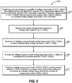
- Figure 2 illustrates an exemplary process 200 employed by the distributed voltage network circuit 100 in Figure 1 to calculate the average voltage (V AVG ) of the distributed load circuit 104 by averaging voltages provided to multiple areas of the distributed load circuit 104.
- the voltage distribution source component 106 distributes a source voltage to the plurality of voltage load nodes 110(1)-110(N) via the distributed source distribution network 112 (block 202).
- the distributed source distribution network 112 includes the plurality of resistive interconnects 114(1)-114(M) interconnecting each source node 108(1)-108(N) to a corresponding voltage load node 110(1)-110(N).
- each voltage load node 110(1)-110(N) receives the source voltage (block 204).
- the distributed voltage network circuit 100 determines a voltage present at each voltage load node 110(1)-110(N) via each corresponding voltage tap node 116(1)-116(N) employed within the distributed source distribution network 112 (block 206).
- the voltage at each voltage tap node 116(1)-116(N) is provided to the input node 118(1)-118(N) of each corresponding resistive element 120(1)-120(N) in the voltage averaging circuit 102 (block 208).
- the voltage averaging circuit 102 provides the voltage on the output node 122(1)-122(N) of each resistive element 120(1)-120(N) to the voltage output node 124, which is configured to provide the average voltage (V AVG ) across the voltage load nodes 110(1)-110(N) of the distributed load circuit 104 (block 210).
- Employing the process 200 allows the distributed voltage network circuit 100 to calculate the average voltage (V AVG ), which may be used to more accurately calculate the current in the distributed load circuit 104, as compared to calculating the current using a voltage present in only one of the voltage load nodes 110(1)-110(N).
- a distributed voltage network circuit similar to the distributed voltage network circuit 100 may employ distributed transistors, wherein a distributed source distribution network similar to the distributed source distribution network 112 includes multiple transistors.
- Figure 3 illustrates an n-type metal-oxide semiconductor (NMOS) distributed voltage network circuit 300, wherein a distributed source distribution network 302 employs NMOS transistors 304(1)-304(N).
- NMOS n-type metal-oxide semiconductor
- NMOS transistors 304(1)-304(N) are in the distributed source distribution network 302 in this aspect, the NMOS transistors 304(1)-304(N) may be located in other elements in other aspects.
- Each NMOS transistor 304(1)-304(N) is coupled to a corresponding source node 306(1)-306(N) of a voltage distribution source component 308 via a corresponding drain 310(1)-310(N).
- the distributed source distribution network 302 includes a plurality of resistive interconnects 312(1)-312(M) that, in conjunction with the NMOS transistors 304(1)-304(N), connect each source node 306(1)-306(N) to a corresponding voltage load node 314(1)-314(N) of a distributed load circuit 316. Particularly, a source 318(1)-318(N) of each corresponding NMOS transistor 304(1)-304(N) couples to the corresponding voltage load node 314(1)-314(N). Further, voltage provided to a gate 320 of the NMOS distributed voltage network circuit 300 controls each NMOS transistor 304(1)-304(N). Voltage tap nodes 322(1)-322(N) are employed within the distributed source distribution network 302 to access the voltage from each corresponding source 318(1)-318(N), and by extension, each voltage load node 314(1)-314(N).
- each voltage tap node 322(1)-322(N) is coupled to an input node 324(1)-324(N) of a corresponding resistor 326(1)-326(N) in a voltage averaging circuit 328.
- An output node 330(1)-330(N) of each resistor 326(1)-326(N) is coupled to a voltage output node 332 of the voltage averaging circuit 328.
- V AVG average voltage (V AVG ) of the distributed load circuit 316 on a voltage output node 332.
- V AVG average voltage in terms of the resistance R of each resistor 326(1)-326(N) and voltage V at each voltage tap node 322(1)-322(N):
- V AVG R 326 1 ⁇ R 326 2 ⁇ ... R 326 N ⁇ V 322 1 / R 326 1 + V 322 2 / R 326 2 + ... V 322 N / R 326 N
- the above equation describes the average voltage (V AVG ) on the voltage output node 332 when the gate width of one or more NMOS transistors 304(1)-304(N) is not approximately equal to the gate width of every other NMOS transistor 304(N)-304(N), as well as when each NMOS transistor 304(1)-304(N) has an approximately equal gate width.
- each resistor 326(1)-326(N) may not have an approximately equal resistance R.
- each resistor 326(1)-326(N) must have an appropriate resistance R in relation to the gate width of the corresponding NMOS transistor 304(1)-304(N) so that the equation described above accurately calculates the average voltage (V AVG ). Further, if each NMOS transistor 304(1)-304(N) has an approximately equal gate width, each resistor 326(1)-326(N) must have an approximately equal resistance R to accurately calculate the average voltage (V AVG ).
- the voltage averaging circuit 328 may also employ a scaling resistor 334.
- the scaling resistor 334 has an input node 336 coupled to a ground source 338, and an output node 340 coupled to the output node 330(1)-330(N) of each resistor 326(1)-326(N).
- the scaling resistor 334 may be used to scale the average voltage (V AVG ) by a scaling factor corresponding to the resistance of the scaling resistor 334 as compared to the average voltage (V AVG ) generated when the scaling resistor 334 is not employed.
- the average voltage may be used to more accurately calculate the current in the distributed load circuit 316, as compared to calculating the current using a voltage at only one of the voltage load nodes 314(1)-314(N).
- a more accurate current measurement may improve functions within a corresponding control system that use the current measurement to increase system performance.
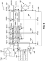
- FIG. 3 illustrates a p-type metal-oxide semiconductor (PMOS) distributed voltage network circuit 400, wherein a distributed source distribution network 402 employs PMOS transistors 404(1)-404(N).
- PMOS metal-oxide semiconductor
- the PMOS transistors 404(1)-404(N) are in the distributed source distribution network 402 in this aspect, the PMOS transistors 404(1)-404(N) may be located in other elements in other aspects.
- Each PMOS transistor 404(1)-404(N) is coupled to a corresponding source node 406(1)-406(N) of a voltage distribution source component 408 via a corresponding source 410(1)-410(N). Similar to the distributed source distribution network 302 in Figure 3 , the distributed source distribution network 402 employs a plurality of resistive interconnects 412(1)-412(M) that, in conjunction with the PMOS transistor 404(1)-404(N), connect each source node 406(1)-406(N) to a corresponding voltage load node 414(1)-414(N) of a distributed load circuit 416.
- a drain 418(1)-418(N) of each corresponding PMOS transistor 404(1)-404(N) couples to the corresponding voltage load node 414(1)-414(N).
- voltage provided to a gate 420 of the PMOS distributed voltage network circuit 400 controls each PMOS transistor 404(1)-404(N).
- Voltage tap nodes 422(1)-422(N) are employed within the distributed source distribution network 402 to access the voltage from each corresponding drain 418(1)-418(N), and thus, each voltage load node 414(1)-414(N).
- each voltage tap node 422(1)-422(N) is coupled to an input node 424(1)-424(N) of a corresponding resistor 426(1)-426(N) in a voltage averaging circuit 428.
- An output node 430(1)-430(N) of each resistor 426(1)-426(N) is coupled to a voltage output node 432 of the voltage averaging circuit 428.
- coupling each output node 430(1)-430(N) while each input node 424(1)-424(N) is coupled to a corresponding voltage tap node 422(1)-422(N) generates the average voltage (V AVG ) of the distributed load circuit 416 on the voltage output node 432.
- a scaling resistor 434 similar to the scaling resistor 334 in Figure 3 may be employed in the PMOS distributed voltage network circuit 400 to scale the average voltage (V AVG ). Further, the equations and associated gate width/resistance relationships previously described in relation to Figure 3 also apply when calculating the average voltage (V AVG ) in Figure 4 . In this manner, the average voltage (V AVG ) may be used to more accurately calculate the current in the distributed load circuit 416, as compared to calculating the current using a voltage at only one of the voltage load nodes 414(1)-414(N).
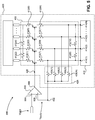
- FIG. 5 illustrates a PMOS distributed voltage network circuit 500, wherein the gate 420 of the PMOS distributed voltage network circuit 400 in Figure 4 is coupled to a voltage regulator circuit 502.
- a reference voltage V REF is provided to a first input 504 of the voltage regulator circuit 502, while the voltage output node 432 of the voltage averaging circuit 428 is coupled to a second input 506 of the voltage regulator circuit 502.
- An output node 508 of the voltage regulator circuit 502 is coupled to the gate 420 of the PMOS distributed voltage network circuit 400.
- the resistors 426(1)-426(N) sample the voltages across the distributed load circuit 416 as previously described, thus providing the average voltage (V AVG ) of the distributed load circuit 416 to the voltage regulator circuit 502.
- the voltage regulator circuit 502 which is an operational amplifier ("op-amp") in this aspect, forces the average voltage (V AVG ) provided to the distributed load circuit 416 to equal V REF .
- the output node 508 provides a voltage to the gate 420 so that the voltage provided to the distributed load circuit 416 is regulated to V REF .
- the voltages on the voltage load nodes 414(1)-414(N) may vary depending on factors such as the resistance of the resistive interconnects 412(0)-412(M) and the physical size and layout of the distributed load circuit 416.
- V AVG average voltage
- the average voltage may be used to more accurately calculate the current in a distributed load circuit.
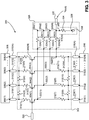
- Figure 6 illustrates an on-die current measurement system 600 that yields better performance when employing voltage averaging circuits similar to the voltage averaging circuits 102, 328, and 428 in Figures 1 , 3 , and 4 , respectively.
- the on-die current measurement system 600 is used to measure a power supply current (not shown) of a distributed load circuit 602, wherein the distributed load circuit 602 may be, as non-limiting examples, a processor core or a cache memory.
- the on-die current measurement system 600 includes a voltage source (V dd ) 604 that provides an input voltage to a source of each headswitch transistor 606(1)-606(N).
- the headswitch transistors 606(1)-606(N) provide power control to the distributed load circuit 602 by allowing a voltage signal 608 to reach corresponding voltage load nodes 610(1)-610(N) on the distributed load circuit 602.
- the voltage source 604 also provides an input voltage to a source of each mirror transistor 612(1)-612(N).
- Each mirror transistor 612(1)-612(N) width is a fraction (f) of the width of the corresponding headswitch transistor 606(1)-606(N).
- the headswitch transistors 606(1)-606(N) and the mirror transistors 612(1)-612(N) are biased deep in the field effect transistor (FET) triode region, effectively making them function as low value resistors.
- FET field effect transistor
- the headswitch transistors 606(1)-606(N) and the mirror transistors 612(1)-612(N) are employed as PMOS transistors in this aspect, other aspects may employ the headswitch transistors 606(1)-606(N) and the mirror transistors 612(1)-612(N) as NMOS transistors.
- a voltage provided by each mirror transistor 612(1)-612(N) traverses a corresponding cascode transistor 614(1)-614(N) into a sense resistor 616.
- a voltage from the sense resistor 616 is provided to an analog-to-digital converter (ADC) 618, which converts the voltage into a digital data stream 620 that represents the power supply current of the distributed load circuit 602.
- ADC analog-to-digital converter
- the headswitch transistors 606(1)-606(N) and the mirror transistors 612(1)-612(N) need to have precisely equal drain-source voltages.
- an op-amp 622 together with the cascode transistors 614(1)-614(N), forces the drain-source voltage of the mirror transistors 612(1)-612(N) to equal that of the headswitch transistors 606(1)-606(N).
- the op-amp 622 controls the cascode transistors 614(1)-614(N) in order to keep the current on the mirror transistors 612(1)-612(N) equal to a fraction (f) of the current on the headswitch transistors 606(1)-606(N). In doing so, the drain-source voltages of the mirror transistors 612(1)-612(N) and the headswitch transistors 606(1)-606(N) are kept equal to one another.
- this aspect illustrates the headswitch transistors 606(1)-606(N), the mirror transistors 612(1)-612(N), and the cascode transistors 614(1)-614(N) as PMOS transistors in Figure 6 , but other aspects may employ other types of transistors to achieve similar functionality.
- the headswitch transistors 606(1)-606(N) are distributed so as to couple to the distributed load circuit 602 at the corresponding voltage load nodes 610(1)-610(N) via headswitch resistive interconnects (not shown) within a distributed source distribution network (not shown).
- a headswitch voltage averaging circuit 624 is employed to provide an average headswitch voltage (V HSAVG ) (not shown) to a first input 626 of the op-amp 622 by way of a headswitch voltage output node 628.
- the mirror transistors 612(1)-612(N) each couple to the corresponding cascode transistor 614(1)-614(N) via mirror resistive interconnects (not shown) within the distributed source distribution network.
- a mirror voltage averaging circuit 630 is employed to provide an average mirror voltage (V MRAVG ) (not shown) to a second input 632 of the op-amp 622 by way of a mirror voltage output node 634.
- V MRAVG average mirror voltage
- Both the headswitch voltage averaging circuit 624 and the mirror voltage averaging circuit 630 include similar elements to the voltage averaging circuits 102, 328, and 428 in Figures 1 , 3 , and 4 , respectively.
- resistors 636(1)-636(N) in the headswitch voltage averaging circuit 624 couple to a corresponding headswitch voltage tap node 638(1)-638(N) within the distributed source distribution network, and are configured to provide the average headswitch voltage (V HSAVG ) to the first input 626 of the op-amp 622.
- Resistors 640(1)-640(N) in the mirror voltage averaging circuit 630 couple to corresponding mirror voltage tap nodes 642(1)-642(N) within the distributed source distribution network, and are configured to provide the average mirror voltage (V MRAVG ) to the second input 632 of the op-amp 622.
- the sense resistor 616 receives a voltage from which to more accurately calculate the current in the distributed load circuit 602, as compared to calculating the current using a voltage from one of the voltage load nodes 610(1)-610(N).
- the headswitch voltage averaging circuit 624 and the mirror voltage averaging circuit 630 may each employ an additional resistor to scale the average headswitch voltage (V HSAVG ) and the average mirror voltage (V MRAVG ), respectively, if desired. More specifically, the headswitch voltage averaging circuit 624 may employ a scaling resistor 644, similar to the scaling resistor 334 in Figure 3 . In this manner, the scaling resistor 644 may be used to scale the headswitch average voltage (V HSAVG ) by a scaling factor corresponding to the resistance of the scaling resistor 644 as compared to the headswitch average voltage (V HSAVG ) generated when the scaling resistor 644 is not employed.
- the mirror voltage averaging circuit 630 may employ a scaling resistor 646 in a similar manner as the headswitch voltage averaging circuit 624 to scale the average mirror voltage (V MRAVG ).
- the on-die current measurement system 600 may also be configured to regulate the load voltage and current provided to the distributed load circuit 602.
- a voltage regulator circuit 648 that is configured to regulate the voltage, and thus the current, provided across the distributed load circuit 602 may be employed in the on-die current measurement system 600.
- the voltage regulator circuit 648 is configured to operate similar to the voltage regulator circuit 502 in Figure 5 . In this manner, by receiving the reference voltage V REF and the average headswitch voltage (V HSAVG ), the voltage regulator circuit 648 provides a voltage to the distributed load circuit 602 that is approximately equal to the reference voltage V REF . Regulating the load voltage provided to the distributed load circuit 602 in this manner may help to ensure that the load voltage of the distributed load circuit 602 is maintained approximately at a desired level.
- test circuits may be used to generate sample data.
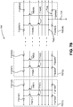
- Figure 7A illustrates a first test circuit 700 that employs headswitch tiles 702(1)-702(48).
- a resistor 704(1)-704(48) is coupled to a corresponding headswitch transistor 706(1)-706(48) to generate an average test headswitch voltage (V THSAVG ) in a similar manner to the headswitch voltage averaging circuit 624 in Figure 6 .
- a resistor 708(1)-708(48) is coupled to a corresponding mirror transistor 710(1)-710(48) to generate an average test mirror voltage (V TMRAVG ) in a similar manner to the mirror voltage averaging circuit 630 in Figure 6 .
- a plurality of parasitic resistors 712(1)(1)-712(48)(4) are included in the first test circuit 700 to simulate interconnection resistance.
- a cascode transistor 714(1)-714(48) corresponding to each mirror transistor 710(1)-710(48) is also included in each headswitch tile 702(1)-702(48). In this manner, currents from the cascode transistors 714(1)-714(48) are summed up and provided to a sense resistor 716.
- Figure 7B illustrates a second test circuit 700' that employs headswitch tiles 702'(1)-702'(48).
- Each headswitch tile 702'(1)-702'(48) includes a corresponding headswitch transistor 706(1)-706(48) and a corresponding mirror transistor 710(1)-710(48) similar to the first test circuit 700 in Figure 7A .
- the plurality of parasitic resistors 712(1)(1)-712(48)(4), as well as the cascode transistors 714(1)-714(48), are also included in the second test circuit 700'.
- the headswitch tiles 702'(1)-702'(48) do not include resistors 704(1)-704(48) and 708(1)-708(48) coupled to corresponding headswitch transistors 706(1)-706(48) and mirror transistors 710(1)-710(48), respectively, as in the first test circuit 700 in Figure 7A .
- the second test circuit 700' does not generate an average test headswitch voltage (V THSAVG ) and an average test mirror voltage (V TMRAVG ). Rather, a headswitch voltage (V HS ) and a mirror voltage (V MR ) is measured at the headswitch tile 702'(48). Currents from the cascode transistors 714(1)-714(48) are summed up and provided to a sense resistor 716'.
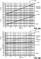
- Figure 8A illustrates an exemplary set of signals 800 corresponding to average current measured across the first and second test circuits 700, 700' in Figures 7A and 7B with ideal non-resistive metal interconnects.
- each parasitic resistor 712(1)(1)-712(48)(4) has a resistance equal to zero Ohms (0 ⁇ ) so as to remove any effect the parasitic resistors 712(1)(1)-712(48)(4) may have on the distributed voltage.
- each sense resistor 716, 716' has a resistance equal to 300 Ohms ( ⁇ ).
- a voltage (V SENSE1 ) across the sense resistor 716, and a voltage (V SENSE2 ) across the sense resistor 716', are both illustrated in a first graph 802.
- the voltage (V SENSE1 ) and the voltage V SENSE2 are approximately equal at multiple current values. For example, at a maximum current of 1.5 A, as indicated by arrow 804, both (V SENSE1 ) and (V SENSE2 ) are approximately equal to 374 mV. This is evidenced in a second graph 806 that illustrates the difference in the values between (V SENSE1 ) and (V SENSE2 ). More specifically, the maximum difference existing between (V SENSE1 ) and (V SENSE2 ) occurs at 1.5 A, wherein the difference is approximately only 160 ⁇ V (microVolts), as indicated by arrow 808.
- the first test circuit 700 and the second test circuit 700' generate close to an effectively ideal voltage across the respective sense resistors 716, 716' of approximately 374 mV.
- Figure 8B illustrates an exemplary set of signals 800' corresponding to average current measured across first and second test circuits 700, 700' in Figures 7A and 7B with non-ideal resistive metal interconnects.
- each parasitic resistor 712(1)(1)-712(48)(4) has a a non-zero Ohm resistance in this aspect.
- the voltage (V SENSE1 ) and the voltage (V SENSE2 ) are both illustrated in a first graph 802'.
- the values of (V SENSE1 ) and (V SENSE2 ) are not equal at varying levels of current, as in Figure 8A .
- (V SENSE1 ) has a value approximately equal to 374 mV, as indicated by arrow 810, which is the same value of (V SENSE1 ) in the ideal case described in Figure 8A .
- (V SENSE2 ) has a value approximately equal to 63 mV, as indicated by arrow 812.
- This difference in values is further illustrated in a second graph 806', which shows that the maximum difference existing between (V SENSE1 ) and (V SENSE2 ) again occurs at 1.5 A, wherein the difference is approximately 311 mV, as indicated by arrow 814.
- a value of 63 mV for (V SENSE2 ) represents a "measured" current of 252 mA, as compared to the actual current of 1.5 A.
- comparing the ideal case illustrated in Figure 8A to the more realistic case illustrated in Figure 8B demonstrates that employing voltage averaging in the first test circuit 700 essentially eliminates variation in measured voltage and current based on varying current distribution profiles across a load circuit. More specifically, under the realistic conditions in Figure 8B , the second test circuit 700' provides a voltage and current that is far below those generated under the ideal conditions in Figure 8A . However, under the realistic conditions in Figure 8B , the first test circuit 700 generates a voltage and current that are approximately equal to those generated under the ideal conditions in Figure 8A . In other words, the first test circuit 700 measures the average voltage, while the second test circuit 700' measures a voltage at a single voltage load node.
- the first test circuit 700 provides a consistent average voltage measurement, while the second test circuit 700' provides varying voltages depending on from which voltage load node the voltage is measured. Therefore, employing voltage averaging as disclosed herein may be used to more accurately calculate the current in a distributed load circuit, as compared to calculating the current using a voltage present in a single voltage load node.
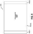
- Figure 9 illustrates a system 900 wherein headswitch circuits 902(1), 902(2) are distributed around a processor core 904 so as to measure average load voltage of the processor core 904.
- Each headswitch circuit 902(1), 902(2) includes a plurality of headswitch tiles similar to the headswitch tiles 702 in Figure 7A .
- the processor core 904 includes a plurality of digital circuits, each of which may be active at varying times. Because the various digital circuits within the processor core 904 may be active at different times, the voltage and current distribution throughout the processor core 904 and headswitch circuits 902(1), 902(2) may vary dramatically over time.
- the voltage averaging mechanism included in the headswitch circuits 902(1), 902(2), as described in previous figures, and particularly in Figure 7A measures the average core voltage (V CAVG ) distributed in the processor core 904. Therefore, the average core voltage (V CAVG ) may be used to more accurately calculate the current distributed in the processor core 904, as compared to calculating the current using a voltage at only one location at a single point in time.
- the distributed voltage network circuits employing voltage averaging according to aspects disclosed herein may be provided in or integrated into any processor-based device. Examples, without limitation, include a set top box, an entertainment unit, a navigation device, a communications device, a fixed location data unit, a mobile location data unit, a mobile phone, a cellular phone, a computer, a portable computer, a desktop computer, a personal digital assistant (PDA), a monitor, a computer monitor, a television, a tuner, a radio, a satellite radio, a music player, a digital music player, a portable music player, a digital video player, a video player, a digital video disc (DVD) player, and a portable digital video player.
- PDA personal digital assistant
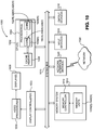
- Figure 10 illustrates an example of a processor-based system 1000 that can employ the voltage averaging circuits 102, 328, and 428 illustrated in Figures 1 , 3 , and 4 , respectively.
- the processor-based system 1000 includes one or more central processing units (CPUs) 1002, each including one or more processors 1004.
- CPUs central processing units
- Each of the one or more processors 1004 may employ a plurality of cores 1006(0)-1006(N), wherein the average load voltage and load current of each core 1006(0)-1006(N) may be calculated using a corresponding voltage averaging circuit, such as the voltage averaging circuits 102(0)-102(N), 328(0)-328(N), or 428(0)-428(N).
- the CPU(s) 1002 may be a master device.
- the CPU(s) 1002 may have cache memory 1008 coupled to the processor(s) 1004 for rapid access to temporarily stored data.
- the CPU(s) 1002 is coupled to a system bus 1010 and can intercouple master and slave devices included in the processor-based system 1000. As is well known, the CPU(s) 1002 communicates with these other devices by exchanging address, control, and data information over the system bus 1010. For example, the CPU(s) 1002 can communicate bus transaction requests to a memory controller 1012 as an example of a slave device.
- a memory controller 1012 as an example of a slave device.
- multiple system buses 1010 could be provided, wherein each system bus 1010 constitutes a different fabric.
- Other master and slave devices can be connected to the system bus 1010. As illustrated in Figure 10 , these devices can include a memory system 1014, one or more input devices 1016, one or more output devices 1018, one or more network interface devices 1020, and one or more display controllers 1022, as examples.
- the input device(s) 1016 can include any type of input device, including but not limited to input keys, switches, voice processors, etc.
- the output device(s) 1018 can include any type of output device, including but not limited to audio, video, other visual indicators, etc.
- the network interface device(s) 1020 can be any devices configured to allow exchange of data to and from a network 1024.
- the network 1024 can be any type of network, including but not limited to a wired or wireless network, a private or public network, a local area network (LAN), a wide local area network (WLAN), and the Internet.
- the network interface device(s) 1020 can be configured to support any type of communications protocol desired.
- the memory system 1014 can include one or more memory units 1026(0)-1026(N).
- the CPU(s) 1002 may also be configured to access the display controller(s) 1022 over the system bus 1010 to control information sent to one or more displays 1028.
- the display controller(s) 1022 sends information to the display(s) 1028 to be displayed via one or more video processors 1030, which process the information to be displayed into a format suitable for the display(s) 1028.
- the display(s) 1028 can include any type of display, including but not limited to a cathode ray tube (CRT), a liquid crystal display (LCD), a plasma display, etc.
- DSP Digital Signal Processor
- ASIC Application Specific Integrated Circuit
- FPGA Field Programmable Gate Array
- a processor may be a microprocessor, but in the alternative, the processor may be any conventional processor, controller, microcontroller, or state machine.
- a processor may also be implemented as a combination of computing devices, e.g., a combination of a DSP and a microprocessor, a plurality of microprocessors, one or more microprocessors in conjunction with a DSP core, or any other such configuration.
- RAM Random Access Memory
- ROM Read Only Memory
- EPROM Electrically Programmable ROM
- EEPROM Electrically Erasable Programmable ROM
- registers a hard disk, a removable disk, a CD-ROM, or any other form of computer readable medium known in the art.
- An exemplary storage medium is coupled to the processor such that the processor can read information from, and write information to, the storage medium.
- the storage medium may be integral to the processor.
- the processor and the storage medium may reside in an ASIC.
- the ASIC may reside in a remote station.
- the processor and the storage medium may reside as discrete components in a remote station, base station, or server.
Landscapes
- Engineering & Computer Science (AREA)
- General Physics & Mathematics (AREA)
- Physics & Mathematics (AREA)
- Manufacturing & Machinery (AREA)
- Electromagnetism (AREA)
- Radar, Positioning & Navigation (AREA)
- Automation & Control Theory (AREA)
- Microelectronics & Electronic Packaging (AREA)
- Computer Hardware Design (AREA)
- Power Engineering (AREA)
- General Engineering & Computer Science (AREA)
- Measurement Of Current Or Voltage (AREA)
- Semiconductor Integrated Circuits (AREA)
- Control Of Electrical Variables (AREA)
- Charge And Discharge Circuits For Batteries Or The Like (AREA)
Applications Claiming Priority (2)
| Application Number | Priority Date | Filing Date | Title |
|---|---|---|---|
| US14/482,456 US9494957B2 (en) | 2014-09-10 | 2014-09-10 | Distributed voltage network circuits employing voltage averaging, and related systems and methods |
| PCT/US2015/046067 WO2016039962A1 (en) | 2014-09-10 | 2015-08-20 | Distributed voltage network circuits employing voltage averaging, and related systems and methods |
Publications (2)
| Publication Number | Publication Date |
|---|---|
| EP3191858A1 EP3191858A1 (en) | 2017-07-19 |
| EP3191858B1 true EP3191858B1 (en) | 2021-01-20 |
Family
ID=54072974
Family Applications (1)
| Application Number | Title | Priority Date | Filing Date |
|---|---|---|---|
| EP15762830.6A Active EP3191858B1 (en) | 2014-09-10 | 2015-08-20 | Distributed voltage network circuits employing voltage averaging, and related systems and methods |
Country Status (10)
| Country | Link |
|---|---|
| US (1) | US9494957B2 (enExample) |
| EP (1) | EP3191858B1 (enExample) |
| JP (1) | JP6702945B2 (enExample) |
| KR (1) | KR102331244B1 (enExample) |
| CN (1) | CN106662888B (enExample) |
| BR (1) | BR112017004693B1 (enExample) |
| CA (1) | CA2957035C (enExample) |
| ES (1) | ES2861265T3 (enExample) |
| TW (1) | TWI594538B (enExample) |
| WO (1) | WO2016039962A1 (enExample) |
Families Citing this family (10)
| Publication number | Priority date | Publication date | Assignee | Title |
|---|---|---|---|---|
| US10345834B2 (en) * | 2017-08-09 | 2019-07-09 | Qualcomm Incorporated | Sensing total current of distributed load circuits independent of current distribution using distributed voltage averaging |
| US11047946B2 (en) | 2018-05-08 | 2021-06-29 | Qualcomm Incorporated | Differential current sensing with robust path, voltage offset removal and process, voltage, temperature (PVT) tolerance |
| US10958167B2 (en) | 2018-08-08 | 2021-03-23 | Qualcomm Incorporated | Current sensing in an on-die direct current-direct current (DC-DC) converter for measuring delivered power |
| US11099238B2 (en) * | 2019-03-27 | 2021-08-24 | General Electric Company | Distributed control modules with built-in tests and control-preserving fault responses |
| KR102639597B1 (ko) | 2020-08-06 | 2024-02-23 | 양쯔 메모리 테크놀로지스 씨오., 엘티디. | 3차원 메모리를 위한 멀티-다이 피크 전력 관리 |
| US11625054B2 (en) * | 2021-06-17 | 2023-04-11 | Novatek Microelectronics Corp. | Voltage to current converter of improved size and accuracy |
| US12153087B2 (en) | 2021-06-25 | 2024-11-26 | Ic Analytica, Llc | Apparatus and method for testing all test circuits on a wafer from a single test site |
| JP2023043717A (ja) * | 2021-09-16 | 2023-03-29 | キオクシア株式会社 | 半導体装置及び半導体集積回路 |
| US12066959B2 (en) * | 2022-05-12 | 2024-08-20 | Intel Corporation | Provisioning a reference voltage based on an evaluation of a pseudo-precision resistor of an IC die |
| US20230398878A1 (en) * | 2022-06-14 | 2023-12-14 | Ford Global Technologies, Llc | Control of gate drive resistance based on radio frequency interference |
Citations (1)
| Publication number | Priority date | Publication date | Assignee | Title |
|---|---|---|---|---|
| US20140097828A1 (en) * | 2006-02-17 | 2014-04-10 | Broadcom Corporation | Current-Monitoring Apparatus |
Family Cites Families (19)
| Publication number | Priority date | Publication date | Assignee | Title |
|---|---|---|---|---|
| JPS5038437A (enExample) * | 1973-08-08 | 1975-04-09 | ||
| US3934209A (en) * | 1974-04-23 | 1976-01-20 | Minnesota Mining And Manufacturing Company | High voltage DC coupled amplifier |
| DE3500676A1 (de) * | 1985-01-11 | 1986-07-17 | Robert Bosch Gmbh, 7000 Stuttgart | Einrichtung zur kontrolle von elektrischen verbrauchern in kraftfahrzeugen |
| DE4237122C2 (de) | 1992-11-03 | 1996-12-12 | Texas Instruments Deutschland | Schaltungsanordnung zur Überwachung des Drainstromes eines Metall-Oxid-Halbleiter-Feldeffekttransistors |
| US5600578A (en) * | 1993-08-02 | 1997-02-04 | Advanced Micro Devices, Inc. | Test method for predicting hot-carrier induced leakage over time in short-channel IGFETs and products designed in accordance with test results |
| US6191966B1 (en) | 1999-12-20 | 2001-02-20 | Texas Instruments Incorporated | Phase current sensor using inverter leg shunt resistor |
| US6461880B1 (en) * | 2001-06-28 | 2002-10-08 | Advanced Micro Devices, Inc. | Method for monitoring silicide failures |
| DE10258766B4 (de) * | 2002-12-16 | 2005-08-25 | Infineon Technologies Ag | Schaltungsanordnung zur Steuerung und Erfassung des Laststroms durch eine Last |
| US6937178B1 (en) | 2003-05-15 | 2005-08-30 | Linear Technology Corporation | Gradient insensitive split-core digital to analog converter |
| US7718448B1 (en) | 2005-05-27 | 2010-05-18 | National Semiconductor Corporation | Method of monitoring process misalignment to reduce asymmetric device operation and improve the electrical and hot carrier performance of LDMOS transistor arrays |
| JP2009123926A (ja) * | 2007-11-15 | 2009-06-04 | Seiko Epson Corp | 基準電圧発生回路、ad変換器、da変換器、および画像処理装置 |
| EP2113656B1 (en) * | 2008-04-29 | 2011-08-31 | GM Global Technology Operations LLC | A method and an apparatus for controlling glow plugs in a diesel engine, particularly for motor-vehicles |
| CN102246115B (zh) * | 2008-11-25 | 2014-04-02 | 凌力尔特有限公司 | 用于半导体芯片内金属电阻器的温度补偿的电路、调修和布图 |
| WO2012147139A1 (ja) * | 2011-04-26 | 2012-11-01 | パナソニック株式会社 | 半導体集積回路システムおよびそれを備えた電子機器、電気製品、移動体 |
| DE102011108738B3 (de) | 2011-07-28 | 2012-12-06 | Texas Instruments Deutschland Gmbh | Laststromabtastschaltung und Verfahren |
| CN102955492B (zh) * | 2011-08-18 | 2014-12-10 | 祥硕科技股份有限公司 | 参考电流产生电路 |
| US8890601B2 (en) * | 2011-11-11 | 2014-11-18 | Qualcomm Incorporated | Method, system, and circuit with a driver output interface having a common mode connection coupled to a transistor bulk connection |
| FR2995696B1 (fr) | 2012-09-19 | 2015-05-29 | Commissariat Energie Atomique | Circuit de mesure de tension differentielle |
| WO2014126496A1 (en) * | 2013-02-14 | 2014-08-21 | Freescale Semiconductor, Inc. | Voltage regulator with improved load regulation |
-
2014
- 2014-09-10 US US14/482,456 patent/US9494957B2/en active Active
-
2015
- 2015-08-17 TW TW104126735A patent/TWI594538B/zh active
- 2015-08-20 ES ES15762830T patent/ES2861265T3/es active Active
- 2015-08-20 JP JP2017512369A patent/JP6702945B2/ja active Active
- 2015-08-20 CN CN201580047060.1A patent/CN106662888B/zh active Active
- 2015-08-20 BR BR112017004693-8A patent/BR112017004693B1/pt active IP Right Grant
- 2015-08-20 KR KR1020177006358A patent/KR102331244B1/ko active Active
- 2015-08-20 CA CA2957035A patent/CA2957035C/en active Active
- 2015-08-20 WO PCT/US2015/046067 patent/WO2016039962A1/en not_active Ceased
- 2015-08-20 EP EP15762830.6A patent/EP3191858B1/en active Active
Patent Citations (1)
| Publication number | Priority date | Publication date | Assignee | Title |
|---|---|---|---|---|
| US20140097828A1 (en) * | 2006-02-17 | 2014-04-10 | Broadcom Corporation | Current-Monitoring Apparatus |
Also Published As
| Publication number | Publication date |
|---|---|
| CA2957035A1 (en) | 2016-03-17 |
| TWI594538B (zh) | 2017-08-01 |
| JP2017533410A (ja) | 2017-11-09 |
| KR20170056531A (ko) | 2017-05-23 |
| EP3191858A1 (en) | 2017-07-19 |
| ES2861265T3 (es) | 2021-10-06 |
| CA2957035C (en) | 2022-12-13 |
| CN106662888B (zh) | 2019-02-22 |
| BR112017004693A2 (pt) | 2017-12-05 |
| KR102331244B1 (ko) | 2021-11-24 |
| WO2016039962A1 (en) | 2016-03-17 |
| JP6702945B2 (ja) | 2020-06-03 |
| TW201618409A (zh) | 2016-05-16 |
| CN106662888A (zh) | 2017-05-10 |
| US9494957B2 (en) | 2016-11-15 |
| US20160070277A1 (en) | 2016-03-10 |
| BR112017004693B1 (pt) | 2022-06-21 |
Similar Documents
| Publication | Publication Date | Title |
|---|---|---|
| EP3191858B1 (en) | Distributed voltage network circuits employing voltage averaging, and related systems and methods | |
| US20190195700A1 (en) | MIDDLE-OF-LINE (MOL) METAL RESISTOR TEMPERATURE SENSORS FOR LOCALIZED TEMPERATURE SENSING OF ACTIVE SEMICONDUCTOR AREAS IN INTEGRATED CIRCUITS (ICs) | |
| CN106935527B (zh) | 电迁移签核方法和系统 | |
| CN110352395B (zh) | 用于集成电路装置的改进的电流感测 | |
| US20150103866A1 (en) | DIGITAL TEMPERATURE ESTIMATORS (DTEs) DISPOSED IN INTEGRATED CIRCUITS (ICs) FOR ESTIMATING TEMPERATURE WITHIN THE ICs, AND RELATED SYSTEMS AND METHODS | |
| EP3665488B1 (en) | Sensing total current of distributed load circuits independent of current distribution using distributed voltage averaging | |
| CN101183398A (zh) | 用于表征器件自加热的结构和方法 | |
| US9514999B2 (en) | Systems and methods for semiconductor line scribe line centering | |
| US20230366746A1 (en) | Multi-Sensing PTAT for Multiple-Location Temperature Sensing | |
| CN110617894A (zh) | 一种集成电路中金属线温度测量方法 | |
| JP2021532600A (ja) | 複数の感知トランジスタに結合されたパワートランジスタ | |
| US7212064B1 (en) | Methods and systems for measuring temperature using digital signals | |
| CN110610871B (zh) | 一种金属栅温度测量方法 | |
| BR112020002255B1 (pt) | Detecção de corrente total de circuitos de carga distribuída independentes da distribuição de corrente usando-se promediação de tensão distribuída | |
| JP2007322205A (ja) | 信頼性試験装置 | |
| CN118783924A (zh) | 以高精度监测工艺、电压及温度的超紧凑及微功率电路 | |
| HK40018433B (en) | Sensing total current of distributed load circuits using distributed voltage averaging circuits | |
| HK40018433A (en) | Sensing total current of distributed load circuits using distributed voltage averaging circuits | |
| Sandha et al. | FTGMOS: A novel feedback thermal gradient MOS circuit model | |
| Labun | Thermally-coupled IC interconnect networks |
Legal Events
| Date | Code | Title | Description |
|---|---|---|---|
| STAA | Information on the status of an ep patent application or granted ep patent |
Free format text: STATUS: THE INTERNATIONAL PUBLICATION HAS BEEN MADE |
|
| PUAI | Public reference made under article 153(3) epc to a published international application that has entered the european phase |
Free format text: ORIGINAL CODE: 0009012 |
|
| STAA | Information on the status of an ep patent application or granted ep patent |
Free format text: STATUS: REQUEST FOR EXAMINATION WAS MADE |
|
| 17P | Request for examination filed |
Effective date: 20170125 |
|
| AK | Designated contracting states |
Kind code of ref document: A1 Designated state(s): AL AT BE BG CH CY CZ DE DK EE ES FI FR GB GR HR HU IE IS IT LI LT LU LV MC MK MT NL NO PL PT RO RS SE SI SK SM TR |
|
| AX | Request for extension of the european patent |
Extension state: BA ME |
|
| RIN1 | Information on inventor provided before grant (corrected) |
Inventor name: SHAH, DHAVAL RAJESHBHAI Inventor name: KOLLA, YESHWANT NAGARAJ Inventor name: PRICE, BURT LEE |
|
| DAV | Request for validation of the european patent (deleted) | ||
| DAX | Request for extension of the european patent (deleted) | ||
| STAA | Information on the status of an ep patent application or granted ep patent |
Free format text: STATUS: EXAMINATION IS IN PROGRESS |
|
| 17Q | First examination report despatched |
Effective date: 20200226 |
|
| GRAP | Despatch of communication of intention to grant a patent |
Free format text: ORIGINAL CODE: EPIDOSNIGR1 |
|
| STAA | Information on the status of an ep patent application or granted ep patent |
Free format text: STATUS: GRANT OF PATENT IS INTENDED |
|
| RIC1 | Information provided on ipc code assigned before grant |
Ipc: G01R 31/30 20060101AFI20200805BHEP Ipc: G05F 1/46 20060101ALI20200805BHEP Ipc: H01L 21/66 20060101ALI20200805BHEP Ipc: G01R 19/00 20060101ALI20200805BHEP |
|
| RIN1 | Information on inventor provided before grant (corrected) |
Inventor name: KOLLA, YESHWANT NAGARAJ Inventor name: SHAH, DHAVAL RAJESHBHAI Inventor name: PRICE, BURT LEE |
|
| INTG | Intention to grant announced |
Effective date: 20200908 |
|
| GRAS | Grant fee paid |
Free format text: ORIGINAL CODE: EPIDOSNIGR3 |
|
| GRAA | (expected) grant |
Free format text: ORIGINAL CODE: 0009210 |
|
| STAA | Information on the status of an ep patent application or granted ep patent |
Free format text: STATUS: THE PATENT HAS BEEN GRANTED |
|
| AK | Designated contracting states |
Kind code of ref document: B1 Designated state(s): AL AT BE BG CH CY CZ DE DK EE ES FI FR GB GR HR HU IE IS IT LI LT LU LV MC MK MT NL NO PL PT RO RS SE SI SK SM TR |
|
| REG | Reference to a national code |
Ref country code: GB Ref legal event code: FG4D |
|
| REG | Reference to a national code |
Ref country code: CH Ref legal event code: EP |
|
| REG | Reference to a national code |
Ref country code: DE Ref legal event code: R096 Ref document number: 602015064966 Country of ref document: DE |
|
| REG | Reference to a national code |
Ref country code: AT Ref legal event code: REF Ref document number: 1356863 Country of ref document: AT Kind code of ref document: T Effective date: 20210215 Ref country code: CH Ref legal event code: NV Representative=s name: MAUCHER JENKINS PATENTANWAELTE AND RECHTSANWAE, DE |
|
| REG | Reference to a national code |
Ref country code: IE Ref legal event code: FG4D |
|
| REG | Reference to a national code |
Ref country code: NL Ref legal event code: FP |
|
| REG | Reference to a national code |
Ref country code: SE Ref legal event code: TRGR |
|
| REG | Reference to a national code |
Ref country code: LT Ref legal event code: MG9D |
|
| REG | Reference to a national code |
Ref country code: AT Ref legal event code: MK05 Ref document number: 1356863 Country of ref document: AT Kind code of ref document: T Effective date: 20210120 |
|
| PG25 | Lapsed in a contracting state [announced via postgrant information from national office to epo] |
Ref country code: PT Free format text: LAPSE BECAUSE OF FAILURE TO SUBMIT A TRANSLATION OF THE DESCRIPTION OR TO PAY THE FEE WITHIN THE PRESCRIBED TIME-LIMIT Effective date: 20210520 Ref country code: LT Free format text: LAPSE BECAUSE OF FAILURE TO SUBMIT A TRANSLATION OF THE DESCRIPTION OR TO PAY THE FEE WITHIN THE PRESCRIBED TIME-LIMIT Effective date: 20210120 Ref country code: BG Free format text: LAPSE BECAUSE OF FAILURE TO SUBMIT A TRANSLATION OF THE DESCRIPTION OR TO PAY THE FEE WITHIN THE PRESCRIBED TIME-LIMIT Effective date: 20210420 Ref country code: NO Free format text: LAPSE BECAUSE OF FAILURE TO SUBMIT A TRANSLATION OF THE DESCRIPTION OR TO PAY THE FEE WITHIN THE PRESCRIBED TIME-LIMIT Effective date: 20210420 Ref country code: FI Free format text: LAPSE BECAUSE OF FAILURE TO SUBMIT A TRANSLATION OF THE DESCRIPTION OR TO PAY THE FEE WITHIN THE PRESCRIBED TIME-LIMIT Effective date: 20210120 Ref country code: GR Free format text: LAPSE BECAUSE OF FAILURE TO SUBMIT A TRANSLATION OF THE DESCRIPTION OR TO PAY THE FEE WITHIN THE PRESCRIBED TIME-LIMIT Effective date: 20210421 Ref country code: HR Free format text: LAPSE BECAUSE OF FAILURE TO SUBMIT A TRANSLATION OF THE DESCRIPTION OR TO PAY THE FEE WITHIN THE PRESCRIBED TIME-LIMIT Effective date: 20210120 |
|
| PG25 | Lapsed in a contracting state [announced via postgrant information from national office to epo] |
Ref country code: RS Free format text: LAPSE BECAUSE OF FAILURE TO SUBMIT A TRANSLATION OF THE DESCRIPTION OR TO PAY THE FEE WITHIN THE PRESCRIBED TIME-LIMIT Effective date: 20210120 Ref country code: LV Free format text: LAPSE BECAUSE OF FAILURE TO SUBMIT A TRANSLATION OF THE DESCRIPTION OR TO PAY THE FEE WITHIN THE PRESCRIBED TIME-LIMIT Effective date: 20210120 Ref country code: PL Free format text: LAPSE BECAUSE OF FAILURE TO SUBMIT A TRANSLATION OF THE DESCRIPTION OR TO PAY THE FEE WITHIN THE PRESCRIBED TIME-LIMIT Effective date: 20210120 Ref country code: AT Free format text: LAPSE BECAUSE OF FAILURE TO SUBMIT A TRANSLATION OF THE DESCRIPTION OR TO PAY THE FEE WITHIN THE PRESCRIBED TIME-LIMIT Effective date: 20210120 |
|
| PG25 | Lapsed in a contracting state [announced via postgrant information from national office to epo] |
Ref country code: IS Free format text: LAPSE BECAUSE OF FAILURE TO SUBMIT A TRANSLATION OF THE DESCRIPTION OR TO PAY THE FEE WITHIN THE PRESCRIBED TIME-LIMIT Effective date: 20210520 |
|
| REG | Reference to a national code |
Ref country code: ES Ref legal event code: FG2A Ref document number: 2861265 Country of ref document: ES Kind code of ref document: T3 Effective date: 20211006 |
|
| REG | Reference to a national code |
Ref country code: DE Ref legal event code: R097 Ref document number: 602015064966 Country of ref document: DE |
|
| PG25 | Lapsed in a contracting state [announced via postgrant information from national office to epo] |
Ref country code: EE Free format text: LAPSE BECAUSE OF FAILURE TO SUBMIT A TRANSLATION OF THE DESCRIPTION OR TO PAY THE FEE WITHIN THE PRESCRIBED TIME-LIMIT Effective date: 20210120 Ref country code: CZ Free format text: LAPSE BECAUSE OF FAILURE TO SUBMIT A TRANSLATION OF THE DESCRIPTION OR TO PAY THE FEE WITHIN THE PRESCRIBED TIME-LIMIT Effective date: 20210120 Ref country code: SM Free format text: LAPSE BECAUSE OF FAILURE TO SUBMIT A TRANSLATION OF THE DESCRIPTION OR TO PAY THE FEE WITHIN THE PRESCRIBED TIME-LIMIT Effective date: 20210120 |
|
| PLBE | No opposition filed within time limit |
Free format text: ORIGINAL CODE: 0009261 |
|
| STAA | Information on the status of an ep patent application or granted ep patent |
Free format text: STATUS: NO OPPOSITION FILED WITHIN TIME LIMIT |
|
| PG25 | Lapsed in a contracting state [announced via postgrant information from national office to epo] |
Ref country code: SK Free format text: LAPSE BECAUSE OF FAILURE TO SUBMIT A TRANSLATION OF THE DESCRIPTION OR TO PAY THE FEE WITHIN THE PRESCRIBED TIME-LIMIT Effective date: 20210120 Ref country code: DK Free format text: LAPSE BECAUSE OF FAILURE TO SUBMIT A TRANSLATION OF THE DESCRIPTION OR TO PAY THE FEE WITHIN THE PRESCRIBED TIME-LIMIT Effective date: 20210120 Ref country code: RO Free format text: LAPSE BECAUSE OF FAILURE TO SUBMIT A TRANSLATION OF THE DESCRIPTION OR TO PAY THE FEE WITHIN THE PRESCRIBED TIME-LIMIT Effective date: 20210120 |
|
| 26N | No opposition filed |
Effective date: 20211021 |
|
| PG25 | Lapsed in a contracting state [announced via postgrant information from national office to epo] |
Ref country code: AL Free format text: LAPSE BECAUSE OF FAILURE TO SUBMIT A TRANSLATION OF THE DESCRIPTION OR TO PAY THE FEE WITHIN THE PRESCRIBED TIME-LIMIT Effective date: 20210120 |
|
| PG25 | Lapsed in a contracting state [announced via postgrant information from national office to epo] |
Ref country code: SI Free format text: LAPSE BECAUSE OF FAILURE TO SUBMIT A TRANSLATION OF THE DESCRIPTION OR TO PAY THE FEE WITHIN THE PRESCRIBED TIME-LIMIT Effective date: 20210120 |
|
| PG25 | Lapsed in a contracting state [announced via postgrant information from national office to epo] |
Ref country code: MC Free format text: LAPSE BECAUSE OF FAILURE TO SUBMIT A TRANSLATION OF THE DESCRIPTION OR TO PAY THE FEE WITHIN THE PRESCRIBED TIME-LIMIT Effective date: 20210120 |
|
| REG | Reference to a national code |
Ref country code: BE Ref legal event code: MM Effective date: 20210831 |
|
| PG25 | Lapsed in a contracting state [announced via postgrant information from national office to epo] |
Ref country code: IS Free format text: LAPSE BECAUSE OF FAILURE TO SUBMIT A TRANSLATION OF THE DESCRIPTION OR TO PAY THE FEE WITHIN THE PRESCRIBED TIME-LIMIT Effective date: 20210520 Ref country code: LU Free format text: LAPSE BECAUSE OF NON-PAYMENT OF DUE FEES Effective date: 20210820 |
|
| PG25 | Lapsed in a contracting state [announced via postgrant information from national office to epo] |
Ref country code: IE Free format text: LAPSE BECAUSE OF NON-PAYMENT OF DUE FEES Effective date: 20210820 Ref country code: BE Free format text: LAPSE BECAUSE OF NON-PAYMENT OF DUE FEES Effective date: 20210831 |
|
| PG25 | Lapsed in a contracting state [announced via postgrant information from national office to epo] |
Ref country code: HU Free format text: LAPSE BECAUSE OF FAILURE TO SUBMIT A TRANSLATION OF THE DESCRIPTION OR TO PAY THE FEE WITHIN THE PRESCRIBED TIME-LIMIT; INVALID AB INITIO Effective date: 20150820 |
|
| PG25 | Lapsed in a contracting state [announced via postgrant information from national office to epo] |
Ref country code: CY Free format text: LAPSE BECAUSE OF FAILURE TO SUBMIT A TRANSLATION OF THE DESCRIPTION OR TO PAY THE FEE WITHIN THE PRESCRIBED TIME-LIMIT Effective date: 20210120 |
|
| PG25 | Lapsed in a contracting state [announced via postgrant information from national office to epo] |
Ref country code: MK Free format text: LAPSE BECAUSE OF FAILURE TO SUBMIT A TRANSLATION OF THE DESCRIPTION OR TO PAY THE FEE WITHIN THE PRESCRIBED TIME-LIMIT Effective date: 20210120 |
|
| PG25 | Lapsed in a contracting state [announced via postgrant information from national office to epo] |
Ref country code: MT Free format text: LAPSE BECAUSE OF FAILURE TO SUBMIT A TRANSLATION OF THE DESCRIPTION OR TO PAY THE FEE WITHIN THE PRESCRIBED TIME-LIMIT Effective date: 20210120 |
|
| PGFP | Annual fee paid to national office [announced via postgrant information from national office to epo] |
Ref country code: NL Payment date: 20250711 Year of fee payment: 11 |
|
| PGFP | Annual fee paid to national office [announced via postgrant information from national office to epo] |
Ref country code: ES Payment date: 20250908 Year of fee payment: 11 |
|
| PGFP | Annual fee paid to national office [announced via postgrant information from national office to epo] |
Ref country code: DE Payment date: 20250709 Year of fee payment: 11 |
|
| PGFP | Annual fee paid to national office [announced via postgrant information from national office to epo] |
Ref country code: IT Payment date: 20250811 Year of fee payment: 11 |
|
| PGFP | Annual fee paid to national office [announced via postgrant information from national office to epo] |
Ref country code: GB Payment date: 20250710 Year of fee payment: 11 |
|
| PGFP | Annual fee paid to national office [announced via postgrant information from national office to epo] |
Ref country code: FR Payment date: 20250709 Year of fee payment: 11 |
|
| PGFP | Annual fee paid to national office [announced via postgrant information from national office to epo] |
Ref country code: CH Payment date: 20250901 Year of fee payment: 11 Ref country code: SE Payment date: 20250808 Year of fee payment: 11 |
|
| PG25 | Lapsed in a contracting state [announced via postgrant information from national office to epo] |
Ref country code: TR Free format text: LAPSE BECAUSE OF FAILURE TO SUBMIT A TRANSLATION OF THE DESCRIPTION OR TO PAY THE FEE WITHIN THE PRESCRIBED TIME-LIMIT Effective date: 20210120 |