EP3188235A1 - Arraysubstrat und herstellungsverfahren dafür, anzeigetafel und anzeigevorrichtung - Google Patents
Arraysubstrat und herstellungsverfahren dafür, anzeigetafel und anzeigevorrichtung Download PDFInfo
- Publication number
- EP3188235A1 EP3188235A1 EP14891131.6A EP14891131A EP3188235A1 EP 3188235 A1 EP3188235 A1 EP 3188235A1 EP 14891131 A EP14891131 A EP 14891131A EP 3188235 A1 EP3188235 A1 EP 3188235A1
- Authority
- EP
- European Patent Office
- Prior art keywords
- electrode
- layer
- via hole
- common electrode
- base substrate
- Prior art date
- Legal status (The legal status is an assumption and is not a legal conclusion. Google has not performed a legal analysis and makes no representation as to the accuracy of the status listed.)
- Granted
Links
- 239000000758 substrate Substances 0.000 title claims abstract description 176
- 238000004519 manufacturing process Methods 0.000 title 1
- 239000002184 metal Substances 0.000 claims abstract description 121
- 238000002161 passivation Methods 0.000 claims abstract description 80
- 238000000034 method Methods 0.000 claims abstract description 49
- 239000010408 film Substances 0.000 description 23
- 230000000149 penetrating effect Effects 0.000 description 12
- 238000010586 diagram Methods 0.000 description 5
- 239000000463 material Substances 0.000 description 4
- 238000000576 coating method Methods 0.000 description 3
- 238000005530 etching Methods 0.000 description 3
- 230000001681 protective effect Effects 0.000 description 3
- 239000010409 thin film Substances 0.000 description 3
- 239000011248 coating agent Substances 0.000 description 2
- 238000005516 engineering process Methods 0.000 description 2
- 239000004973 liquid crystal related substance Substances 0.000 description 2
- 230000008878 coupling Effects 0.000 description 1
- 238000010168 coupling process Methods 0.000 description 1
- 238000005859 coupling reaction Methods 0.000 description 1
- 230000005855 radiation Effects 0.000 description 1
- 238000004544 sputter deposition Methods 0.000 description 1
Images


Classifications
-
- H—ELECTRICITY
- H01—ELECTRIC ELEMENTS
- H01L—SEMICONDUCTOR DEVICES NOT COVERED BY CLASS H10
- H01L27/00—Devices consisting of a plurality of semiconductor or other solid-state components formed in or on a common substrate
- H01L27/02—Devices consisting of a plurality of semiconductor or other solid-state components formed in or on a common substrate including semiconductor components specially adapted for rectifying, oscillating, amplifying or switching and having at least one potential-jump barrier or surface barrier; including integrated passive circuit elements with at least one potential-jump barrier or surface barrier
- H01L27/12—Devices consisting of a plurality of semiconductor or other solid-state components formed in or on a common substrate including semiconductor components specially adapted for rectifying, oscillating, amplifying or switching and having at least one potential-jump barrier or surface barrier; including integrated passive circuit elements with at least one potential-jump barrier or surface barrier the substrate being other than a semiconductor body, e.g. an insulating body
- H01L27/1214—Devices consisting of a plurality of semiconductor or other solid-state components formed in or on a common substrate including semiconductor components specially adapted for rectifying, oscillating, amplifying or switching and having at least one potential-jump barrier or surface barrier; including integrated passive circuit elements with at least one potential-jump barrier or surface barrier the substrate being other than a semiconductor body, e.g. an insulating body comprising a plurality of TFTs formed on a non-semiconducting substrate, e.g. driving circuits for AMLCDs
- H01L27/124—Devices consisting of a plurality of semiconductor or other solid-state components formed in or on a common substrate including semiconductor components specially adapted for rectifying, oscillating, amplifying or switching and having at least one potential-jump barrier or surface barrier; including integrated passive circuit elements with at least one potential-jump barrier or surface barrier the substrate being other than a semiconductor body, e.g. an insulating body comprising a plurality of TFTs formed on a non-semiconducting substrate, e.g. driving circuits for AMLCDs with a particular composition, shape or layout of the wiring layers specially adapted to the circuit arrangement, e.g. scanning lines in LCD pixel circuits
-
- G—PHYSICS
- G02—OPTICS
- G02F—OPTICAL DEVICES OR ARRANGEMENTS FOR THE CONTROL OF LIGHT BY MODIFICATION OF THE OPTICAL PROPERTIES OF THE MEDIA OF THE ELEMENTS INVOLVED THEREIN; NON-LINEAR OPTICS; FREQUENCY-CHANGING OF LIGHT; OPTICAL LOGIC ELEMENTS; OPTICAL ANALOGUE/DIGITAL CONVERTERS
- G02F1/00—Devices or arrangements for the control of the intensity, colour, phase, polarisation or direction of light arriving from an independent light source, e.g. switching, gating or modulating; Non-linear optics
- G02F1/01—Devices or arrangements for the control of the intensity, colour, phase, polarisation or direction of light arriving from an independent light source, e.g. switching, gating or modulating; Non-linear optics for the control of the intensity, phase, polarisation or colour
- G02F1/13—Devices or arrangements for the control of the intensity, colour, phase, polarisation or direction of light arriving from an independent light source, e.g. switching, gating or modulating; Non-linear optics for the control of the intensity, phase, polarisation or colour based on liquid crystals, e.g. single liquid crystal display cells
- G02F1/133—Constructional arrangements; Operation of liquid crystal cells; Circuit arrangements
- G02F1/136—Liquid crystal cells structurally associated with a semi-conducting layer or substrate, e.g. cells forming part of an integrated circuit
- G02F1/1362—Active matrix addressed cells
- G02F1/136227—Through-hole connection of the pixel electrode to the active element through an insulation layer
-
- H—ELECTRICITY
- H01—ELECTRIC ELEMENTS
- H01L—SEMICONDUCTOR DEVICES NOT COVERED BY CLASS H10
- H01L27/00—Devices consisting of a plurality of semiconductor or other solid-state components formed in or on a common substrate
- H01L27/02—Devices consisting of a plurality of semiconductor or other solid-state components formed in or on a common substrate including semiconductor components specially adapted for rectifying, oscillating, amplifying or switching and having at least one potential-jump barrier or surface barrier; including integrated passive circuit elements with at least one potential-jump barrier or surface barrier
- H01L27/12—Devices consisting of a plurality of semiconductor or other solid-state components formed in or on a common substrate including semiconductor components specially adapted for rectifying, oscillating, amplifying or switching and having at least one potential-jump barrier or surface barrier; including integrated passive circuit elements with at least one potential-jump barrier or surface barrier the substrate being other than a semiconductor body, e.g. an insulating body
- H01L27/1214—Devices consisting of a plurality of semiconductor or other solid-state components formed in or on a common substrate including semiconductor components specially adapted for rectifying, oscillating, amplifying or switching and having at least one potential-jump barrier or surface barrier; including integrated passive circuit elements with at least one potential-jump barrier or surface barrier the substrate being other than a semiconductor body, e.g. an insulating body comprising a plurality of TFTs formed on a non-semiconducting substrate, e.g. driving circuits for AMLCDs
- H01L27/124—Devices consisting of a plurality of semiconductor or other solid-state components formed in or on a common substrate including semiconductor components specially adapted for rectifying, oscillating, amplifying or switching and having at least one potential-jump barrier or surface barrier; including integrated passive circuit elements with at least one potential-jump barrier or surface barrier the substrate being other than a semiconductor body, e.g. an insulating body comprising a plurality of TFTs formed on a non-semiconducting substrate, e.g. driving circuits for AMLCDs with a particular composition, shape or layout of the wiring layers specially adapted to the circuit arrangement, e.g. scanning lines in LCD pixel circuits
- H01L27/1244—Devices consisting of a plurality of semiconductor or other solid-state components formed in or on a common substrate including semiconductor components specially adapted for rectifying, oscillating, amplifying or switching and having at least one potential-jump barrier or surface barrier; including integrated passive circuit elements with at least one potential-jump barrier or surface barrier the substrate being other than a semiconductor body, e.g. an insulating body comprising a plurality of TFTs formed on a non-semiconducting substrate, e.g. driving circuits for AMLCDs with a particular composition, shape or layout of the wiring layers specially adapted to the circuit arrangement, e.g. scanning lines in LCD pixel circuits for preventing breakage, peeling or short circuiting
-
- H—ELECTRICITY
- H01—ELECTRIC ELEMENTS
- H01L—SEMICONDUCTOR DEVICES NOT COVERED BY CLASS H10
- H01L27/00—Devices consisting of a plurality of semiconductor or other solid-state components formed in or on a common substrate
- H01L27/02—Devices consisting of a plurality of semiconductor or other solid-state components formed in or on a common substrate including semiconductor components specially adapted for rectifying, oscillating, amplifying or switching and having at least one potential-jump barrier or surface barrier; including integrated passive circuit elements with at least one potential-jump barrier or surface barrier
- H01L27/12—Devices consisting of a plurality of semiconductor or other solid-state components formed in or on a common substrate including semiconductor components specially adapted for rectifying, oscillating, amplifying or switching and having at least one potential-jump barrier or surface barrier; including integrated passive circuit elements with at least one potential-jump barrier or surface barrier the substrate being other than a semiconductor body, e.g. an insulating body
- H01L27/1214—Devices consisting of a plurality of semiconductor or other solid-state components formed in or on a common substrate including semiconductor components specially adapted for rectifying, oscillating, amplifying or switching and having at least one potential-jump barrier or surface barrier; including integrated passive circuit elements with at least one potential-jump barrier or surface barrier the substrate being other than a semiconductor body, e.g. an insulating body comprising a plurality of TFTs formed on a non-semiconducting substrate, e.g. driving circuits for AMLCDs
- H01L27/1248—Devices consisting of a plurality of semiconductor or other solid-state components formed in or on a common substrate including semiconductor components specially adapted for rectifying, oscillating, amplifying or switching and having at least one potential-jump barrier or surface barrier; including integrated passive circuit elements with at least one potential-jump barrier or surface barrier the substrate being other than a semiconductor body, e.g. an insulating body comprising a plurality of TFTs formed on a non-semiconducting substrate, e.g. driving circuits for AMLCDs with a particular composition or shape of the interlayer dielectric specially adapted to the circuit arrangement
-
- H—ELECTRICITY
- H10—SEMICONDUCTOR DEVICES; ELECTRIC SOLID-STATE DEVICES NOT OTHERWISE PROVIDED FOR
- H10K—ORGANIC ELECTRIC SOLID-STATE DEVICES
- H10K59/00—Integrated devices, or assemblies of multiple devices, comprising at least one organic light-emitting element covered by group H10K50/00
- H10K59/10—OLED displays
- H10K59/12—Active-matrix OLED [AMOLED] displays
- H10K59/121—Active-matrix OLED [AMOLED] displays characterised by the geometry or disposition of pixel elements
-
- H—ELECTRICITY
- H10—SEMICONDUCTOR DEVICES; ELECTRIC SOLID-STATE DEVICES NOT OTHERWISE PROVIDED FOR
- H10K—ORGANIC ELECTRIC SOLID-STATE DEVICES
- H10K59/00—Integrated devices, or assemblies of multiple devices, comprising at least one organic light-emitting element covered by group H10K50/00
- H10K59/10—OLED displays
- H10K59/12—Active-matrix OLED [AMOLED] displays
- H10K59/123—Connection of the pixel electrodes to the thin film transistors [TFT]
-
- G—PHYSICS
- G02—OPTICS
- G02F—OPTICAL DEVICES OR ARRANGEMENTS FOR THE CONTROL OF LIGHT BY MODIFICATION OF THE OPTICAL PROPERTIES OF THE MEDIA OF THE ELEMENTS INVOLVED THEREIN; NON-LINEAR OPTICS; FREQUENCY-CHANGING OF LIGHT; OPTICAL LOGIC ELEMENTS; OPTICAL ANALOGUE/DIGITAL CONVERTERS
- G02F1/00—Devices or arrangements for the control of the intensity, colour, phase, polarisation or direction of light arriving from an independent light source, e.g. switching, gating or modulating; Non-linear optics
- G02F1/01—Devices or arrangements for the control of the intensity, colour, phase, polarisation or direction of light arriving from an independent light source, e.g. switching, gating or modulating; Non-linear optics for the control of the intensity, phase, polarisation or colour
- G02F1/13—Devices or arrangements for the control of the intensity, colour, phase, polarisation or direction of light arriving from an independent light source, e.g. switching, gating or modulating; Non-linear optics for the control of the intensity, phase, polarisation or colour based on liquid crystals, e.g. single liquid crystal display cells
- G02F1/133—Constructional arrangements; Operation of liquid crystal cells; Circuit arrangements
- G02F1/136—Liquid crystal cells structurally associated with a semi-conducting layer or substrate, e.g. cells forming part of an integrated circuit
- G02F1/1362—Active matrix addressed cells
- G02F1/136231—Active matrix addressed cells for reducing the number of lithographic steps
-
- G—PHYSICS
- G09—EDUCATION; CRYPTOGRAPHY; DISPLAY; ADVERTISING; SEALS
- G09G—ARRANGEMENTS OR CIRCUITS FOR CONTROL OF INDICATING DEVICES USING STATIC MEANS TO PRESENT VARIABLE INFORMATION
- G09G2300/00—Aspects of the constitution of display devices
- G09G2300/04—Structural and physical details of display devices
- G09G2300/0421—Structural details of the set of electrodes
- G09G2300/0426—Layout of electrodes and connections
Definitions
- Embodiments of the present disclosure relate to an array substrate and a fabricating method thereof, a display panel and a display apparatus.
- a thin film transistor liquid crystal display is a comparatively ideal display device due to advantages of small size, low power consumption, no radiation and so on.
- TFT-LCD thin film transistor liquid crystal display
- HADS Advanced-super Dimensional Switching
- an array substrate of an HADS technology in the state of art comprises a base substrate 1a, a gate electrode 2a, a common electrode line 3a, a gate insulating layer 4a, an active layer 5a, a pixel electrode 6a, a drain electrode 8a, a source electrode 7a, a data line 9a, a passivation layer 10a, and a common electrode 11a; the common electrode 11a is electrically connected with the common electrode line 3 a through a via hole 20a.
- the via hole 20a is a via hole penetrating through both the gate insulating layer 4a and the passivation layer 10a.
- the passivation layer 10a is required to be made thicker, and therefore, to ensure effectiveness of the via hole 20a, a hole depth of the via hole 20a is enough large and the size of the via hole is relatively large.
- the relatively large hole depth and size of the via hole 20a make the coating process of a subsequent fabricating process be difficultly controlled and easily invoke moires on a coated film layer, thereby affecting the yield of the fabricated array substrates.
- an array substrate comprising a base substrate and a gate metal layer, a gate insulating layer, an active layer, a source-drain electrode metal layer, a passivation layer and a common electrode layer which are sequentially formed on the base substrate, as well as a pixel electrode layer which is positioned between the active layer and the source-drain electrode metal layer or between the source-drain electrode metal layer and the passivation layer; the gate metal layer including a gate electrode and a common electrode line.
- the pixel electrode layer or the source-drain electrode metal layer includes a connecting electrode, the connecting electrode is electrically connected with the common electrode line through a first via hole in the gate insulating layer, and the connecting electrode is electrically connected with a common electrode of the common electrode layer through a second via hole in the passivation layer.
- the connecting electrode is in direct contact with the gate insulating layer and the passivation layer.
- vertical projections of the first via hole and the second via hole on the base substrate are mutually staggered, a position of the first via hole corresponds to that of the common electrode line, a position of the second via hole corresponds to that of the common electrode, and the vertical projections of the first via hole and the second via hole on the base substrate fall within a scope of a vertical projection of the connecting electrode on the base substrate.
- the connecting electrode is positioned in the pixel electrode layer, and the connecting electrode is mutually insulated from a pixel electrode of the pixel electrode layer.
- the connecting electrode is positioned in the source-drain electrode metal layer, and the connecting electrode is mutually insulated from a source electrode, a drain electrode and a data line of the source-drain electrode metal layer.
- the display panel comprises the array substrate as described above.
- the display apparatus comprises the display panel as described above.
- a fabricating method of an array substrate comprises: sequentially forming a gate metal layer, a gate insulating layer, an active layer, a source-drain electrode metal layer, a passivation layer and a common electrode layer on a substrate, and forming a pixel electrode layer between the active layer and the source-drain electrode metal layer or between the source-drain electrode metal layer and the passivation layer, the gate metal layer including a gate electrode and a common electrode line.
- the fabricating method further comprises: forming a connecting electrode in the pixel electrode layer or the source-drain electrode metal layer, forming a first via hole in the gate insulating layer, and forming a second via hole in the passivation layer, the connecting electrode being electrically connected with the common electrode line through the first via hole in the gate insulating layer, and the connecting electrode being electrically connected with a common electrode of the common electrode layer through the second via hole in the passivation layer.
- the fabricating method of the array substrate comprises: sequentially forming the gate metal layer on the base substrate, the gate metal layer including a gate electrode and the common electrode line; sequentially forming the gate insulating layer and the active layer on the gate metal layer; forming the first via hole in a region of the gate insulating layer outside the active layer, a position of the first via hole corresponding to that of the common electrode line; forming the pixel electrode layer including a pixel electrode and the connecting electrode on the base substrate, the connecting electrode being electrically connected with the common electrode line through the first via hole; forming the source-drain electrode metal layer including a source electrode, a drain electrode and a data line on the base substrate; forming the passivation layer on the base substrate, the passivation layer including the second via hole corresponding to the connecting electrode; forming the common electrode layer including the common electrode on the base substrate, the common electrode being electrically connected with the connecting electrode through the second via hole.
- the fabricating method of the array substrate comprises: sequentially forming the gate metal layer on the base substrate, the gate metal layer including a gate electrode and the common electrode line; sequentially forming the gate insulating layer and the active layer on the gate metal layer; forming the first via hole in a region of the gate insulating layer outside the active layer, a position of the first via hole corresponding to that of the common electrode line; forming the source-drain electrode metal layer including a source electrode, a drain electrode, a data line and the connecting electrode on the base substrate, the connecting electrode being electrically connected with the common electrode line through the first via hole; forming the pixel electrode layer including a pixel electrode on the base substrate; forming the passivation layer on the base substrate, the passivation layer including the second via hole corresponding to the connecting electrode; forming the common electrode layer including the common electrode on the base substrate, the common electrode being electrically connected with the connecting electrode through the second via hole.
- the fabricating method of the array substrate comprises: sequentially forming the gate metal layer on the base substrate, the gate metal layer including a gate electrode and the common electrode line; forming a gate insulating layer, an active layer and a pixel electrode layer including a pixel electrode on the gate metal layer; forming the first via hole in a region of the gate insulating layer, a position of the first via hole corresponding to that of the common electrode line; forming the source-drain electrode metal layer including a source electrode, a drain electrode, a data line and the connecting electrode on the base substrate, the connecting electrode being electrically connected with the common electrode line through the first via hole; forming a passivation layer on the base substrate, the passivation layer including the second via hole corresponding to the connecting electrode; forming a common electrode layer including the common electrode on the base substrate, the common electrode being electrically connected with the connecting electrode through the second via hole.
- the fabricating method of the array substrate comprises: sequentially forming the gate metal layer on the base substrate, the gate metal layer including a gate electrode and the common electrode line; forming the gate insulating layer, the active layer, and the source-drain electrode metal layer including a source electrode, a drain electrode and a data line on the gate metal layer; forming the first via hole in a region of the gate insulating layer outside the active layer and the data line, a position of the first via hole corresponding to that of the common electrode line; forming the pixel electrode layer including a pixel electrode and the connecting electrode on the base substrate, the connecting electrode being electrically connected with the common electrode line through the first via hole; forming the passivation layer on the base substrate, the passivation layer including the second via hole corresponding to the connecting electrode; forming a common electrode layer including the common electrode on the base substrate, the common electrode being electrically connected with the connecting electrode through the second via hole.
- the connecting electrode is mutually insulated from the pixel electrode.
- the connecting electrode is mutually insulated from the source electrode, the drain electrode and the data line.
- vertical projections of the first via hole and the second via hole on the base substrate are mutually staggered, and the vertical projections of the first via hole and the second via hole on the base substrate fall within a scope of a vertical projection of the connecting electrode on the base substrate.
- An embodiment of the present disclosure provides an array substrate, which comprises a base substrate and a gate metal layer, a gate insulating layer, an active layer, a source-drain electrode metal layer, a passivation layer, and a common electrode layer which are sequentially formed on the base substrate, as well as a pixel electrode layer which is positioned between the active layer and the source-drain electrode metal layer or between the source-drain electrode metal layer and the passivation layer; the gate metal layer includes a gate electrode and a common electrode line.
- the pixel electrode layer or the source-drain electrode metal layer includes a connecting electrode, the connecting electrode is electrically connected with the common electrode line through a first via hole in the gate insulating layer, and the connecting electrode is electrically connected with a common electrode of the common electrode layer through a second via hole in the passivation layer.
- the connecting electrode is electrically connected with the common electrode line through the first via hole, and the common electrode of the common electrode layer is electrically connected with the connecting electrode through the second via hole, so that an electrical connection between the common electrode and the common electrode line is established. Because the first via hole and the second via hole are electrically connected by the connecting electrode, hole depths and sizes of the first via hole and the second via hole are reduced in comparison with those of a continuous via hole directly penetrating through both the gate insulating layer and the passivation layer, the influence on the coated film layer in the subsequent fabricating process is reduced, and moires are prevented from being produced on the coated film layer.
- the connecting electrode is in direct contact with the gate insulating layer and the passivation layer, and is electrically connected with the common electrode line and the common electrode respectively through the first via hole in the gate insulating layer and the second via hole in the passivation layer.
- vertical projections of the first via hole and the second via hole on the base substrate are mutually staggered, the position of the first via hole corresponds to that of the common electrode line, the position of the second via hole corresponds to that of the common electrode, and the vertical projections of the first via hole and the second via hole on the base substrate fall within the scope of a vertical projection of the connecting electrode on the base substrate. Because the vertical projections of the first via hole and the second via hole are in different positions, they are not mutually influenced.
- the connecting electrode is positioned in the pixel electrode layer, and the connecting electrode is mutually insulated from the pixel electrode in the pixel electrode layer.
- the connecting electrode is positioned in the source-drain electrode metal layer, and the connecting electrode is mutually insulated from a source electrode, a drain electrode and a data line in the source-drain electrode metal layer.
- the gate metal layer includes a gate electrode 2 and a common electrode line 3;
- the pixel electrode layer includes a pixel electrode 6;
- the source-drain electrode metal layer includes a source electrode 7, a drain electrode 8 and a data line 9;
- the common electrode layer includes a common electrode 11; and the source electrode 7, the drain electrode 8, the gate electrode 2 and the active layer 5 form a Thin Film Transistor (TFT).
- TFT Thin Film Transistor
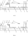
- the pixel electrode layer further includes a connecting electrode 12, the connecting electrode 12 is electrically connected with the common electrode line 3 through a first via hole 13 in the gate insulating layer, and the connecting electrode 12 is electrically connected with the common electrode 11 of the common electrode layer through a second via hole 14 in the passivation layer.
- the connecting electrode 12 and the pixel electrode 6 are arranged in a same layer.
- the connecting electrode 12 is in direct contact with the gate insulating layer 4 and the passivation layer 10 and is arranged outside a region of the active layer 5 and the pixel electrode 6.
- FIG. 2 visually shows a positional relationship of the first via hole 13, the second via hole 14 and the connecting electrode 12. Because the vertical projections of the first via hole 13 and the second via hole 14 are in different positions, they are not mutually influenced.
- the connecting electrode 12 is mutually insulated from the pixel electrode 6.
- the connecting electrode 12 is electrically connected with the common electrode line 3 through the first via hole 13, and the common electrode 11 of the common electrode layer is electrically connected with the connecting electrode 12 through the second via hole 14, so that an electrical connection of the common electrode 11 and the common electrode line 3 is established. Because the first via hole 13 and the second via hole 14 are electrically connected by the connecting electrode 12, hole depths and sizes of the first via hole 13 and the second via hole 14 are reduced in comparison with those of a continuous via hole (via hole 20a as shown in FIG.
- the gate metal layer includes a gate electrode 2 and a common electrode line 3;
- the pixel electrode layer includes a pixel electrode 6;
- the source-drain electrode metal layer includes a source electrode 7, a drain electrode 8 and a data line 9;
- the common electrode layer includes a common electrode 11; and the source electrode 7, the drain electrode 8, the gate electrode 2 and the active layer 5 form a TFT.
- the pixel electrode layer further includes a connecting electrode 12, the connecting electrode 12 is electrically connected with the common electrode line 3 through a first via hole 13 in the gate insulating layer, and the connecting electrode 12 is electrically connected with the common electrode 11 of the common electrode layer through a second via hole 14 in the passivation layer.
- the connecting electrode 12 and the source electrode 7, the drain electrode 8 and the data line 9 are arranged in a same layer.
- the connecting electrode 12 is in direct contact with the gate insulating layer 4 and the passivation layer 10 and is arranged outside a region of the active layer 5 and the pixel electrode 6.
- FIG. 3 visually shows a positional relationship of the first via hole 13, the second via hole 14 and the connecting electrode 12. Because the vertical projections of the first via hole 13 and the second via hole 14 are in different positions, they are not mutually influenced.
- the connecting electrode 12 is mutually insulated from the source electrode 7, the drain electrode 8 and the data line 9.
- the connecting electrode 12 is electrically connected with the common electrode line 3 through the first via hole 13, and the common electrode 11 of the common electrode layer is electrically connected with the connecting electrode 12 through the second via hole 14, so that an electrical connection of the common electrode 11 and the common electrode line 3 is established. Because the first via hole 13 and the second via hole 14 are electrically connected by the connecting electrode 12, hole depths and sizes of the first via hole 13 and the second via hole 14 are reduced in comparison with those of a continuous via hole (via hole 20a as shown in FIG.
- the gate metal layer includes a gate electrode 2 and a common electrode line 3;
- the source-drain electrode metal layer includes a source electrode 7, a drain electrode 8 and a data line 9;
- the pixel electrode layer includes a pixel electrode 6;
- the common electrode layer includes a common electrode 11; and the source electrode 7, the drain electrode 8, the gate electrode 2 and the active layer 5 form a TFT.
- the source-drain electrode metal layer further includes a connecting electrode 12, the connecting electrode 12 is electrically connected with the common electrode line 3 through a first via hole 13 in the gate insulating layer, and the connecting electrode 12 is electrically connected with the common electrode 11 of the common electrode layer through a second via hole 14 in the passivation layer.
- the connecting electrode 12 and the source electrode 7, the drain electrode 8 and the data line 9 are arranged in a same layer.
- the connecting electrode 12 is in direct contact with the gate insulating layer 4 and the passivation layer 10 and is arranged outside a region of the active layer 5 and the pixel electrode 6.
- FIG. 3 visually shows a positional relationship of the first via hole 13, the second via hole 14 and the connecting electrode 12. Because the vertical projections of the first via hole 13 and the second via hole 14 are in different positions, they are not mutually influenced.
- the connecting electrode 12 is mutually insulated from the source electrode 7, the drain electrode 8 and the data line 9.
- the connecting electrode 12 is electrically connected with the common electrode line 3 through the first via hole 13, and the common electrode 11 of the common electrode layer is electrically connected with the connecting electrode 12 through the second via hole 14, so that an electrical connection of the common electrode 11 and the common electrode line 3 is established. Because the first via hole 13 and the second via hole 14 are electrically connected by the connecting electrode 12, hole depths and sizes of the first via hole 13 and the second via hole 14 are reduced in comparison with those of a continuous via hole (via hole 20a as shown in FIG.
- the gate metal layer includes a gate electrode 2 and a common electrode line 3
- the source-drain electrode metal layer includes a source electrode 7, a drain electrode 8 and a data line 9
- the pixel electrode layer includes a pixel electrode 6;
- the common electrode layer includes a common electrode 11; and the source electrode 7, the drain electrode 8, the gate electrode 2 and the active layer 5 form a thin film transistor (TFT).
- TFT thin film transistor
- the pixel electrode layer further includes a connecting electrode 12, the connecting electrode 12 is electrically connected with the common electrode line 3 through a first via hole 13 in the gate insulating layer, and the connecting electrode 12 is electrically connected with the common electrode 11 of the common electrode layer through a second via hole 14 in the passivation layer.
- the connecting electrode 12 and the pixel electrode 6 are arranged in a same layer.
- the connecting electrode 12 is in direct contact with the gate insulating layer 4 and the passivation layer 10 and is arranged outside a region of the active layer 5 and the pixel electrode 6.
- FIG. 2 visually shows a positional relationship of the first via hole 13, the second via hole 14 and the connecting electrode 12. Because the vertical projections of the first via hole 13 and the second via hole 14 are in different positions, they are not mutually influenced.
- the connecting electrode 12 is mutually insulated from the pixel electrode 6.
- the connecting electrode 12 is electrically connected with the common electrode line 3 through the first via hole 13, and the common electrode 11 of the common electrode layer is electrically connected with the connecting electrode 12 through the second via hole 14, so that an electrical connection of the common electrode 11 and the common electrode line 3 is established. Because the first via hole 13 and the second via hole 14 are electrically connected by the connecting electrode 12, hole depths and sizes of the first via hole 13 and the second via hole 14 are reduced in comparison with those of a continuous via hole (via hole 20a as shown in FIG.
- An embodiment of the present disclosure further provides a display panel, comprising the array substrate provided by any of the above embodiments.
- the display panel provided by the embodiment of the present disclosure may further comprise a color filter substrate, a liquid crystal, and other commonly used components, which will not be described in detail herein.
- a pixel electrode layer or a source-drain electrode metal layer is provided with a connecting electrode, the connecting electrode is electrically connected with a common electrode line through a first via hole, and the common electrode is electrically connected with the connecting electrode through a second via hole, so that an electrical connection of the common electrode and the common electrode line is established.
- first via hole and the second via hole are respectively arranged in different layers and are electrically connected through the connecting electrode, hole depths and sizes of the first via hole and the second via hole are reduced in comparison with those of a continuous via hole directly penetrating through both the gate insulating layer and the passivation layer, the influence on the coated film layer in the subsequent fabricating process is reduced, and moires are prevented from being produced on the coated film layer, so that the yield of array substrates is increased.
- An embodiment of the present disclosure further provides a display apparatus, comprising the display panel provided by the above embodiment.
- the display apparatus according to the embodiment of the present disclosure may further comprise a backlight module, a frame, a base and the like, which will not be described in detail herein.
- a connecting electrode is arranged between a gate insulating layer and a passivation layer of the array substrate, the connecting electrode is electrically connected with a common electrode line through a first via hole, and the common electrode is electrically connected with the connecting electrode through a second via hole, so that an electrical connection of the common electrode and the common electrode line is established.
- the first via hole and the second via hole are respectively arranged in different layers and are electrically connected through the connecting electrode, the hole depths and the sizes of the first via hole and the second via hole are reduced in comparison with those of a continuous via hole directly penetrating through both the gate insulating layer and the passivation layer, the influence on the coated film layer in the subsequent fabricating process is reduced, and moires are prevented from being produced on the coated film layer, so that the yield of array substrates is increased.
- An embodiment of the present disclosure further provides a fabricating method of an array substrate.
- the fabricating method comprises: sequentially forming a gate metal layer, a gate insulating layer, an active layer, a source-drain electrode metal layer, a passivation layer and a common electrode layer on a base substrate, and forming a pixel electrode layer between the active layer and the source-drain electrode metal layer or between the source-drain electrode metal layer and the passivation layer, the gate metal layer including a gate electrode and a common electrode line.
- the fabricating method further comprises: forming a connecting electrode in the pixel electrode layer or the source-drain electrode metal layer, forming a first via hole in the gate insulating layer, and forming a second via hole in the passivation layer, the connecting electrode being electrically connected with the common electrode line through the first via hole in the gate insulating layer, and the connecting electrode being electrically connected with a common electrode of the common electrode layer through the second via hole in the passivation layer.
- the fabricating method of the array substrate comprises following steps:
- the structure of the array substrate fabricated by the steps 601-607 is shown in FIG. 2 .
- the connecting electrode is electrically connected with the common electrode line through the first via hole, and the common electrode of the common electrode layer is electrically connected with the connecting electrode through the second via hole, so that an electrical connection of the common electrode and the common electrode line is established.
- first via hole and the second via hole are electrically connected by the connecting electrode, hole depths and sizes of the first via hole and the second via hole are reduced in comparison with those of a continuous via hole directly penetrating through both the gate insulating layer and the passivation layer, the influence on the coated film layer in the subsequent fabricating process is reduced, and moires are prevented from being produced on the coated film layer, so that the yield of array substrates is increased; further, the connecting electrode and the pixel electrode are in a same layer and are synchronously formed, so that fabricating procedures and material consumption are reduced.
- the fabricating method of the array substrate comprises following steps:
- the connecting electrode is electrically connected with the common electrode line through the first via hole, and the common electrode of the common electrode layer is electrically connected with the connecting electrode through the second via hole, so that an electrical connection of the common electrode and the common electrode line is established.
- the connecting electrode Because the first via hole and the second via hole are electrically connected by the connecting electrode, the hole depths and the sizes of the first via hole and the second via hole are reduced in comparison with those of a continuous via hole directly penetrating through both the gate insulating layer and the passivation layer, the influence on the coated film layer in the subsequent fabricating process is reduced, and moires are prevented from being produced on the coated film layer, so that the yield of array substrates is increased; further, the connecting electrode, and the source electrode, the drain electrode and the data line are in a same layer and are synchronously formed, so that fabricating procedures and material consumption are reduced.
- the structure of the array substrate fabricated by the steps 701-707 is shown in FIG. 4 .
- the fabricating method of the array substrate comprises following steps:
- the connecting electrode is electrically connected with the common electrode line through the first via hole, and the common electrode of the common electrode layer is electrically connected with the connecting electrode through the second via hole, so that an electrical connection of the common electrode and the common electrode line is established.
- the connecting electrode and the source electrode, the drain electrode and the data line are in a same layer and are synchronously formed, so that fabricating procedures and material consumption are reduced.
- the structure of the array substrate fabricated by the steps 801-806 is shown in FIG. 3 .
- the fabricating method of the array substrate comprises following steps:
- the connecting electrode arranged in the pixel electrode layer, the connecting electrode is electrically connected with the common electrode line through the first via hole, and the common electrode of the common electrode layer is electrically connected with the connecting electrode through the second via hole, so that an electrical connection of the common electrode and the common electrode line is established.
- the connecting electrode Because the first via hole and the second via hole are electrically connected by the connecting electrode, the hole depths and the sizes of the first via hole and the second via hole are reduced in comparison with those of a continuous via hole directly penetrating through both the gate insulating layer and the passivation layer, the influence on the coated film layer in the subsequent fabricating process is reduced, and moires are prevented from being produced on the coated film layer, so that the yield of array substrates is increased; further, the connecting electrode and the pixel electrode are in a same layer and are synchronously formed, so that fabricating procedures and material consumption are reduced.
- the structure of the array substrate fabricated by the steps 901-906 is shown in FIG. 5 .
- the gate insulating layer and the first via hole therein and the passivation layer and the second via hole therein may be formed by processes such as coating and etching
- the gate metal layer and the source-drain electrode metal layer may be formed by processes such as sputtering, etching and the like
- the active layer, the pixel electrode layer and the common electrode layer may be formed by processes such as coating, etching and the like, which will not be described in detail herein.
Applications Claiming Priority (2)
| Application Number | Priority Date | Filing Date | Title |
|---|---|---|---|
| CN201410438637.9A CN104332473A (zh) | 2014-08-29 | 2014-08-29 | 一种阵列基板、其制备方法、显示面板和显示装置 |
| PCT/CN2014/091555 WO2016029564A1 (zh) | 2014-08-29 | 2014-11-19 | 阵列基板及其制备方法、显示面板和显示装置 |
Publications (3)
| Publication Number | Publication Date |
|---|---|
| EP3188235A1 true EP3188235A1 (de) | 2017-07-05 |
| EP3188235A4 EP3188235A4 (de) | 2018-04-18 |
| EP3188235B1 EP3188235B1 (de) | 2020-05-06 |
Family
ID=52407171
Family Applications (1)
| Application Number | Title | Priority Date | Filing Date |
|---|---|---|---|
| EP14891131.6A Active EP3188235B1 (de) | 2014-08-29 | 2014-11-19 | Arraysubstrat und herstellungsverfahren dafür, anzeigetafel und anzeigevorrichtung |
Country Status (4)
| Country | Link |
|---|---|
| US (1) | US9893091B2 (de) |
| EP (1) | EP3188235B1 (de) |
| CN (1) | CN104332473A (de) |
| WO (1) | WO2016029564A1 (de) |
Families Citing this family (14)
| Publication number | Priority date | Publication date | Assignee | Title |
|---|---|---|---|---|
| CN105047722A (zh) | 2015-08-19 | 2015-11-11 | 京东方科技集团股份有限公司 | 一种薄膜晶体管及其制作方法、阵列基板、显示面板 |
| CN105161505B (zh) * | 2015-09-28 | 2018-11-23 | 京东方科技集团股份有限公司 | 一种阵列基板及其制作方法、显示面板 |
| CN106910731B (zh) * | 2015-12-23 | 2019-01-29 | 创意电子股份有限公司 | 层叠基板结构 |
| CN106129067A (zh) * | 2016-07-18 | 2016-11-16 | 京东方科技集团股份有限公司 | 一种像素结构及其制备方法、阵列基板、显示装置 |
| CN106019751B (zh) | 2016-08-15 | 2020-06-02 | 京东方科技集团股份有限公司 | 阵列基板及其制造方法、显示装置 |
| KR102542594B1 (ko) | 2016-12-16 | 2023-06-14 | 삼성전자 주식회사 | 다층 인쇄 회로 기판 및 이를 포함하는 전자 장치 |
| US10355026B2 (en) * | 2017-06-22 | 2019-07-16 | Shenzhen China Star Optoelectronics Semiconductor Display Technology Co., Ltd. | Method for manufacturing metal wire and array substrate using the same |
| CN107180838B (zh) * | 2017-06-23 | 2019-12-31 | 深圳市华星光电技术有限公司 | 一种阵列基板及其制造方法 |
| CN107134463B (zh) * | 2017-07-03 | 2020-02-21 | 京东方科技集团股份有限公司 | 阵列基板及其制备方法、显示面板 |
| US10566354B2 (en) | 2018-02-26 | 2020-02-18 | Wuhan China Star Optoelectronics Technology Co., Ltd. | Array substrate, touch display screen and manufacturing method of array substrate |
| CN108073331A (zh) * | 2018-02-26 | 2018-05-25 | 武汉华星光电技术有限公司 | 阵列基板、触控显示屏及阵列基板的制备方法 |
| CN111638616B (zh) * | 2019-03-01 | 2022-04-15 | 京东方科技集团股份有限公司 | 显示基板及其制作方法、显示面板及其制作方法 |
| CN110648629B (zh) * | 2019-10-31 | 2023-09-22 | 厦门天马微电子有限公司 | 显示面板及其制作方法、显示装置 |
| CN113838867B (zh) * | 2021-09-22 | 2024-03-08 | 京东方科技集团股份有限公司 | 阵列基板及其制作方法、显示面板、显示装置 |
Family Cites Families (11)
| Publication number | Priority date | Publication date | Assignee | Title |
|---|---|---|---|---|
| TWI633365B (zh) * | 2006-05-16 | 2018-08-21 | 日商半導體能源研究所股份有限公司 | 液晶顯示裝置 |
| CN102681276B (zh) * | 2012-02-28 | 2014-07-09 | 京东方科技集团股份有限公司 | 阵列基板及其制造方法以及包括该阵列基板的显示装置 |
| CN102981335A (zh) * | 2012-11-15 | 2013-03-20 | 京东方科技集团股份有限公司 | 像素单元结构、阵列基板和显示装置 |
| CN202948925U (zh) * | 2012-12-21 | 2013-05-22 | 北京京东方光电科技有限公司 | Tft阵列基板及显示装置 |
| CN103018991B (zh) * | 2012-12-24 | 2015-01-28 | 京东方科技集团股份有限公司 | 一种阵列基板及其制造方法、显示装置 |
| CN103208491B (zh) * | 2013-02-25 | 2015-12-02 | 京东方科技集团股份有限公司 | 阵列基板及其制造方法、显示装置 |
| CN203117620U (zh) * | 2013-03-19 | 2013-08-07 | 北京京东方光电科技有限公司 | Tft阵列基板及显示装置 |
| CN103309108B (zh) | 2013-05-30 | 2016-02-10 | 京东方科技集团股份有限公司 | 阵列基板及其制造方法、显示装置 |
| CN103489877B (zh) * | 2013-09-30 | 2015-12-09 | 北京京东方光电科技有限公司 | 阵列基板及其制造方法和显示装置 |
| CN103715138B (zh) * | 2013-12-31 | 2017-01-25 | 京东方科技集团股份有限公司 | 一种阵列基板及其制造方法、显示装置 |
| CN104037126A (zh) | 2014-05-16 | 2014-09-10 | 京东方科技集团股份有限公司 | 一种阵列基板的制备方法、阵列基板和显示装置 |
-
2014
- 2014-08-29 CN CN201410438637.9A patent/CN104332473A/zh active Pending
- 2014-11-19 EP EP14891131.6A patent/EP3188235B1/de active Active
- 2014-11-19 WO PCT/CN2014/091555 patent/WO2016029564A1/zh active Application Filing
- 2014-11-19 US US14/771,094 patent/US9893091B2/en active Active
Also Published As
| Publication number | Publication date |
|---|---|
| EP3188235B1 (de) | 2020-05-06 |
| EP3188235A4 (de) | 2018-04-18 |
| WO2016029564A1 (zh) | 2016-03-03 |
| CN104332473A (zh) | 2015-02-04 |
| US20160064415A1 (en) | 2016-03-03 |
| US9893091B2 (en) | 2018-02-13 |
Similar Documents
| Publication | Publication Date | Title |
|---|---|---|
| EP3188235B1 (de) | Arraysubstrat und herstellungsverfahren dafür, anzeigetafel und anzeigevorrichtung | |
| US10658397B2 (en) | Flexible display panel, manufacturing method of flexible display panel and display apparatus | |
| EP2741135A1 (de) | Substrat für tft-lcd-array | |
| US9419027B2 (en) | Array substrate, method for fabricating the same and display device | |
| US20170052418A1 (en) | Array substrate, manufacturing method thereof, liquid crystal display panel and display device | |
| US9543324B2 (en) | Array substrate, display device and manufacturing method of the array substrate | |
| EP3089213B1 (de) | Arraysubstrat, herstellungsverfahren dafür und anzeigevorrichtung | |
| US9798192B2 (en) | Display substrate and manufacturing method thereof, display panel and display device | |
| US20140134809A1 (en) | Method for manufacturing fan-out lines on array substrate | |
| US20160379996A1 (en) | Display Substrate and Manufacturing Method Thereof, and Display Device | |
| EP3151279B1 (de) | Arraysubstrat und herstellungsverfahren dafür und anzeigevorrichtung | |
| US9923067B2 (en) | Thin-film transistor and method for fabricating the same, array substrate and method for fabricating the same, and display device | |
| EP2731127A1 (de) | Tft-array-substrat, herstellungsverfahren dafür und anzeigevorrichtung | |
| US9502576B2 (en) | Thin film transistor and method for manufacturing the same, array substrate, display device | |
| US20160254284A1 (en) | Array substrate, method of preparing the same, and display device | |
| US10551696B2 (en) | Method of producing metal electrode, array substrate and method of producing the same, display device | |
| WO2017008453A1 (en) | Thin film transistor, fabricating method thereof, and display device | |
| US20160322388A1 (en) | Array substrate, its manufacturing method and display device | |
| US9735278B2 (en) | Array substrate, display panel and method of manufacturing thin film transistor | |
| US9196631B1 (en) | Array substrate and method for manufacturing the same, and display device | |
| US10109653B2 (en) | Array substrate, manufacturing method thereof and display device | |
| US20170170212A1 (en) | Thin film transistor array substrate and method of fabricating the same | |
| US9947693B2 (en) | Array substrate, method for manufacturing the same, and display device | |
| US20150228733A1 (en) | Array Substrate, Manufacturing Method Thereof, and Display Device | |
| US8936973B1 (en) | Anodization of gate with laser vias and cuts |
Legal Events
| Date | Code | Title | Description |
|---|---|---|---|
| PUAI | Public reference made under article 153(3) epc to a published international application that has entered the european phase |
Free format text: ORIGINAL CODE: 0009012 |
|
| STAA | Information on the status of an ep patent application or granted ep patent |
Free format text: STATUS: REQUEST FOR EXAMINATION WAS MADE |
|
| 17P | Request for examination filed |
Effective date: 20151112 |
|
| AK | Designated contracting states |
Kind code of ref document: A1 Designated state(s): AL AT BE BG CH CY CZ DE DK EE ES FI FR GB GR HR HU IE IS IT LI LT LU LV MC MK MT NL NO PL PT RO RS SE SI SK SM TR |
|
| AX | Request for extension of the european patent |
Extension state: BA ME |
|
| DAX | Request for extension of the european patent (deleted) | ||
| A4 | Supplementary search report drawn up and despatched |
Effective date: 20180315 |
|
| RIC1 | Information provided on ipc code assigned before grant |
Ipc: H01L 27/12 20060101AFI20180309BHEP Ipc: H01L 21/77 20170101ALI20180309BHEP |
|
| REG | Reference to a national code |
Ref country code: DE Ref legal event code: R079 Ref document number: 602014065296 Country of ref document: DE Free format text: PREVIOUS MAIN CLASS: H01L0027120000 Ipc: G02F0001136200 |
|
| RIC1 | Information provided on ipc code assigned before grant |
Ipc: G02F 1/1362 20060101AFI20191219BHEP |
|
| GRAP | Despatch of communication of intention to grant a patent |
Free format text: ORIGINAL CODE: EPIDOSNIGR1 |
|
| STAA | Information on the status of an ep patent application or granted ep patent |
Free format text: STATUS: GRANT OF PATENT IS INTENDED |
|
| INTG | Intention to grant announced |
Effective date: 20200131 |
|
| GRAS | Grant fee paid |
Free format text: ORIGINAL CODE: EPIDOSNIGR3 |
|
| GRAA | (expected) grant |
Free format text: ORIGINAL CODE: 0009210 |
|
| STAA | Information on the status of an ep patent application or granted ep patent |
Free format text: STATUS: THE PATENT HAS BEEN GRANTED |
|
| AK | Designated contracting states |
Kind code of ref document: B1 Designated state(s): AL AT BE BG CH CY CZ DE DK EE ES FI FR GB GR HR HU IE IS IT LI LT LU LV MC MK MT NL NO PL PT RO RS SE SI SK SM TR |
|
| REG | Reference to a national code |
Ref country code: GB Ref legal event code: FG4D |
|
| REG | Reference to a national code |
Ref country code: CH Ref legal event code: EP Ref country code: AT Ref legal event code: REF Ref document number: 1267729 Country of ref document: AT Kind code of ref document: T Effective date: 20200515 |
|
| REG | Reference to a national code |
Ref country code: IE Ref legal event code: FG4D |
|
| REG | Reference to a national code |
Ref country code: DE Ref legal event code: R096 Ref document number: 602014065296 Country of ref document: DE |
|
| REG | Reference to a national code |
Ref country code: LT Ref legal event code: MG4D |
|
| REG | Reference to a national code |
Ref country code: NL Ref legal event code: MP Effective date: 20200506 |
|
| PG25 | Lapsed in a contracting state [announced via postgrant information from national office to epo] |
Ref country code: PT Free format text: LAPSE BECAUSE OF FAILURE TO SUBMIT A TRANSLATION OF THE DESCRIPTION OR TO PAY THE FEE WITHIN THE PRESCRIBED TIME-LIMIT Effective date: 20200907 Ref country code: IS Free format text: LAPSE BECAUSE OF FAILURE TO SUBMIT A TRANSLATION OF THE DESCRIPTION OR TO PAY THE FEE WITHIN THE PRESCRIBED TIME-LIMIT Effective date: 20200906 Ref country code: NO Free format text: LAPSE BECAUSE OF FAILURE TO SUBMIT A TRANSLATION OF THE DESCRIPTION OR TO PAY THE FEE WITHIN THE PRESCRIBED TIME-LIMIT Effective date: 20200806 Ref country code: GR Free format text: LAPSE BECAUSE OF FAILURE TO SUBMIT A TRANSLATION OF THE DESCRIPTION OR TO PAY THE FEE WITHIN THE PRESCRIBED TIME-LIMIT Effective date: 20200807 Ref country code: FI Free format text: LAPSE BECAUSE OF FAILURE TO SUBMIT A TRANSLATION OF THE DESCRIPTION OR TO PAY THE FEE WITHIN THE PRESCRIBED TIME-LIMIT Effective date: 20200506 Ref country code: SE Free format text: LAPSE BECAUSE OF FAILURE TO SUBMIT A TRANSLATION OF THE DESCRIPTION OR TO PAY THE FEE WITHIN THE PRESCRIBED TIME-LIMIT Effective date: 20200506 Ref country code: LT Free format text: LAPSE BECAUSE OF FAILURE TO SUBMIT A TRANSLATION OF THE DESCRIPTION OR TO PAY THE FEE WITHIN THE PRESCRIBED TIME-LIMIT Effective date: 20200506 |
|
| PG25 | Lapsed in a contracting state [announced via postgrant information from national office to epo] |
Ref country code: BG Free format text: LAPSE BECAUSE OF FAILURE TO SUBMIT A TRANSLATION OF THE DESCRIPTION OR TO PAY THE FEE WITHIN THE PRESCRIBED TIME-LIMIT Effective date: 20200806 Ref country code: RS Free format text: LAPSE BECAUSE OF FAILURE TO SUBMIT A TRANSLATION OF THE DESCRIPTION OR TO PAY THE FEE WITHIN THE PRESCRIBED TIME-LIMIT Effective date: 20200506 Ref country code: LV Free format text: LAPSE BECAUSE OF FAILURE TO SUBMIT A TRANSLATION OF THE DESCRIPTION OR TO PAY THE FEE WITHIN THE PRESCRIBED TIME-LIMIT Effective date: 20200506 Ref country code: HR Free format text: LAPSE BECAUSE OF FAILURE TO SUBMIT A TRANSLATION OF THE DESCRIPTION OR TO PAY THE FEE WITHIN THE PRESCRIBED TIME-LIMIT Effective date: 20200506 |
|
| REG | Reference to a national code |
Ref country code: AT Ref legal event code: MK05 Ref document number: 1267729 Country of ref document: AT Kind code of ref document: T Effective date: 20200506 |
|
| PG25 | Lapsed in a contracting state [announced via postgrant information from national office to epo] |
Ref country code: NL Free format text: LAPSE BECAUSE OF FAILURE TO SUBMIT A TRANSLATION OF THE DESCRIPTION OR TO PAY THE FEE WITHIN THE PRESCRIBED TIME-LIMIT Effective date: 20200506 Ref country code: AL Free format text: LAPSE BECAUSE OF FAILURE TO SUBMIT A TRANSLATION OF THE DESCRIPTION OR TO PAY THE FEE WITHIN THE PRESCRIBED TIME-LIMIT Effective date: 20200506 |
|
| PG25 | Lapsed in a contracting state [announced via postgrant information from national office to epo] |
Ref country code: AT Free format text: LAPSE BECAUSE OF FAILURE TO SUBMIT A TRANSLATION OF THE DESCRIPTION OR TO PAY THE FEE WITHIN THE PRESCRIBED TIME-LIMIT Effective date: 20200506 Ref country code: EE Free format text: LAPSE BECAUSE OF FAILURE TO SUBMIT A TRANSLATION OF THE DESCRIPTION OR TO PAY THE FEE WITHIN THE PRESCRIBED TIME-LIMIT Effective date: 20200506 Ref country code: SM Free format text: LAPSE BECAUSE OF FAILURE TO SUBMIT A TRANSLATION OF THE DESCRIPTION OR TO PAY THE FEE WITHIN THE PRESCRIBED TIME-LIMIT Effective date: 20200506 Ref country code: DK Free format text: LAPSE BECAUSE OF FAILURE TO SUBMIT A TRANSLATION OF THE DESCRIPTION OR TO PAY THE FEE WITHIN THE PRESCRIBED TIME-LIMIT Effective date: 20200506 Ref country code: RO Free format text: LAPSE BECAUSE OF FAILURE TO SUBMIT A TRANSLATION OF THE DESCRIPTION OR TO PAY THE FEE WITHIN THE PRESCRIBED TIME-LIMIT Effective date: 20200506 Ref country code: IT Free format text: LAPSE BECAUSE OF FAILURE TO SUBMIT A TRANSLATION OF THE DESCRIPTION OR TO PAY THE FEE WITHIN THE PRESCRIBED TIME-LIMIT Effective date: 20200506 Ref country code: CZ Free format text: LAPSE BECAUSE OF FAILURE TO SUBMIT A TRANSLATION OF THE DESCRIPTION OR TO PAY THE FEE WITHIN THE PRESCRIBED TIME-LIMIT Effective date: 20200506 Ref country code: ES Free format text: LAPSE BECAUSE OF FAILURE TO SUBMIT A TRANSLATION OF THE DESCRIPTION OR TO PAY THE FEE WITHIN THE PRESCRIBED TIME-LIMIT Effective date: 20200506 |
|
| REG | Reference to a national code |
Ref country code: DE Ref legal event code: R097 Ref document number: 602014065296 Country of ref document: DE |
|
| PG25 | Lapsed in a contracting state [announced via postgrant information from national office to epo] |
Ref country code: PL Free format text: LAPSE BECAUSE OF FAILURE TO SUBMIT A TRANSLATION OF THE DESCRIPTION OR TO PAY THE FEE WITHIN THE PRESCRIBED TIME-LIMIT Effective date: 20200506 Ref country code: SK Free format text: LAPSE BECAUSE OF FAILURE TO SUBMIT A TRANSLATION OF THE DESCRIPTION OR TO PAY THE FEE WITHIN THE PRESCRIBED TIME-LIMIT Effective date: 20200506 |
|
| PLBE | No opposition filed within time limit |
Free format text: ORIGINAL CODE: 0009261 |
|
| STAA | Information on the status of an ep patent application or granted ep patent |
Free format text: STATUS: NO OPPOSITION FILED WITHIN TIME LIMIT |
|
| 26N | No opposition filed |
Effective date: 20210209 |
|
| PG25 | Lapsed in a contracting state [announced via postgrant information from national office to epo] |
Ref country code: SI Free format text: LAPSE BECAUSE OF FAILURE TO SUBMIT A TRANSLATION OF THE DESCRIPTION OR TO PAY THE FEE WITHIN THE PRESCRIBED TIME-LIMIT Effective date: 20200506 |
|
| PG25 | Lapsed in a contracting state [announced via postgrant information from national office to epo] |
Ref country code: MC Free format text: LAPSE BECAUSE OF FAILURE TO SUBMIT A TRANSLATION OF THE DESCRIPTION OR TO PAY THE FEE WITHIN THE PRESCRIBED TIME-LIMIT Effective date: 20200506 |
|
| REG | Reference to a national code |
Ref country code: CH Ref legal event code: PL |
|
| GBPC | Gb: european patent ceased through non-payment of renewal fee |
Effective date: 20201119 |
|
| PG25 | Lapsed in a contracting state [announced via postgrant information from national office to epo] |
Ref country code: LU Free format text: LAPSE BECAUSE OF NON-PAYMENT OF DUE FEES Effective date: 20201119 |
|
| REG | Reference to a national code |
Ref country code: BE Ref legal event code: MM Effective date: 20201130 |
|
| PG25 | Lapsed in a contracting state [announced via postgrant information from national office to epo] |
Ref country code: LI Free format text: LAPSE BECAUSE OF NON-PAYMENT OF DUE FEES Effective date: 20201130 Ref country code: CH Free format text: LAPSE BECAUSE OF NON-PAYMENT OF DUE FEES Effective date: 20201130 |
|
| PG25 | Lapsed in a contracting state [announced via postgrant information from national office to epo] |
Ref country code: IE Free format text: LAPSE BECAUSE OF NON-PAYMENT OF DUE FEES Effective date: 20201119 Ref country code: FR Free format text: LAPSE BECAUSE OF NON-PAYMENT OF DUE FEES Effective date: 20201130 |
|
| PG25 | Lapsed in a contracting state [announced via postgrant information from national office to epo] |
Ref country code: GB Free format text: LAPSE BECAUSE OF NON-PAYMENT OF DUE FEES Effective date: 20201119 |
|
| PG25 | Lapsed in a contracting state [announced via postgrant information from national office to epo] |
Ref country code: TR Free format text: LAPSE BECAUSE OF FAILURE TO SUBMIT A TRANSLATION OF THE DESCRIPTION OR TO PAY THE FEE WITHIN THE PRESCRIBED TIME-LIMIT Effective date: 20200506 Ref country code: MT Free format text: LAPSE BECAUSE OF FAILURE TO SUBMIT A TRANSLATION OF THE DESCRIPTION OR TO PAY THE FEE WITHIN THE PRESCRIBED TIME-LIMIT Effective date: 20200506 Ref country code: CY Free format text: LAPSE BECAUSE OF FAILURE TO SUBMIT A TRANSLATION OF THE DESCRIPTION OR TO PAY THE FEE WITHIN THE PRESCRIBED TIME-LIMIT Effective date: 20200506 |
|
| PG25 | Lapsed in a contracting state [announced via postgrant information from national office to epo] |
Ref country code: MK Free format text: LAPSE BECAUSE OF FAILURE TO SUBMIT A TRANSLATION OF THE DESCRIPTION OR TO PAY THE FEE WITHIN THE PRESCRIBED TIME-LIMIT Effective date: 20200506 |
|
| PG25 | Lapsed in a contracting state [announced via postgrant information from national office to epo] |
Ref country code: BE Free format text: LAPSE BECAUSE OF NON-PAYMENT OF DUE FEES Effective date: 20201130 |
|
| PGFP | Annual fee paid to national office [announced via postgrant information from national office to epo] |
Ref country code: DE Payment date: 20231120 Year of fee payment: 10 |