EP3188174A1 - Pixelansteuerungsschaltung und ansteuerungsverfahren dafür sowie anzeigetafel und anzeigevorrichtung - Google Patents
Pixelansteuerungsschaltung und ansteuerungsverfahren dafür sowie anzeigetafel und anzeigevorrichtung Download PDFInfo
- Publication number
- EP3188174A1 EP3188174A1 EP16823633.9A EP16823633A EP3188174A1 EP 3188174 A1 EP3188174 A1 EP 3188174A1 EP 16823633 A EP16823633 A EP 16823633A EP 3188174 A1 EP3188174 A1 EP 3188174A1
- Authority
- EP
- European Patent Office
- Prior art keywords
- node
- transistor
- terminal
- level
- signal terminal
- Prior art date
- Legal status (The legal status is an assumption and is not a legal conclusion. Google has not performed a legal analysis and makes no representation as to the accuracy of the status listed.)
- Withdrawn
Links
- 238000000034 method Methods 0.000 title claims abstract description 18
- 238000004146 energy storage Methods 0.000 claims abstract description 33
- 239000003990 capacitor Substances 0.000 claims description 17
- 241001270131 Agaricus moelleri Species 0.000 claims description 9
- 238000004519 manufacturing process Methods 0.000 abstract description 6
- 238000005516 engineering process Methods 0.000 abstract description 2
- 238000010586 diagram Methods 0.000 description 13
- 230000008569 process Effects 0.000 description 5
- 230000008859 change Effects 0.000 description 4
- 230000000694 effects Effects 0.000 description 3
- 229920001621 AMOLED Polymers 0.000 description 2
- 230000003321 amplification Effects 0.000 description 2
- 230000001419 dependent effect Effects 0.000 description 2
- 230000004048 modification Effects 0.000 description 2
- 238000012986 modification Methods 0.000 description 2
- 238000003199 nucleic acid amplification method Methods 0.000 description 2
- 239000010409 thin film Substances 0.000 description 2
- 230000032683 aging Effects 0.000 description 1
- 230000005669 field effect Effects 0.000 description 1
- 238000007667 floating Methods 0.000 description 1
- 230000007774 longterm Effects 0.000 description 1
- 230000005855 radiation Effects 0.000 description 1
Images


Classifications
-
- G—PHYSICS
- G09—EDUCATION; CRYPTOGRAPHY; DISPLAY; ADVERTISING; SEALS
- G09G—ARRANGEMENTS OR CIRCUITS FOR CONTROL OF INDICATING DEVICES USING STATIC MEANS TO PRESENT VARIABLE INFORMATION
- G09G3/00—Control arrangements or circuits, of interest only in connection with visual indicators other than cathode-ray tubes
- G09G3/20—Control arrangements or circuits, of interest only in connection with visual indicators other than cathode-ray tubes for presentation of an assembly of a number of characters, e.g. a page, by composing the assembly by combination of individual elements arranged in a matrix no fixed position being assigned to or needed to be assigned to the individual characters or partial characters
- G09G3/22—Control arrangements or circuits, of interest only in connection with visual indicators other than cathode-ray tubes for presentation of an assembly of a number of characters, e.g. a page, by composing the assembly by combination of individual elements arranged in a matrix no fixed position being assigned to or needed to be assigned to the individual characters or partial characters using controlled light sources
- G09G3/30—Control arrangements or circuits, of interest only in connection with visual indicators other than cathode-ray tubes for presentation of an assembly of a number of characters, e.g. a page, by composing the assembly by combination of individual elements arranged in a matrix no fixed position being assigned to or needed to be assigned to the individual characters or partial characters using controlled light sources using electroluminescent panels
- G09G3/32—Control arrangements or circuits, of interest only in connection with visual indicators other than cathode-ray tubes for presentation of an assembly of a number of characters, e.g. a page, by composing the assembly by combination of individual elements arranged in a matrix no fixed position being assigned to or needed to be assigned to the individual characters or partial characters using controlled light sources using electroluminescent panels semiconductive, e.g. using light-emitting diodes [LED]
- G09G3/3208—Control arrangements or circuits, of interest only in connection with visual indicators other than cathode-ray tubes for presentation of an assembly of a number of characters, e.g. a page, by composing the assembly by combination of individual elements arranged in a matrix no fixed position being assigned to or needed to be assigned to the individual characters or partial characters using controlled light sources using electroluminescent panels semiconductive, e.g. using light-emitting diodes [LED] organic, e.g. using organic light-emitting diodes [OLED]
- G09G3/3225—Control arrangements or circuits, of interest only in connection with visual indicators other than cathode-ray tubes for presentation of an assembly of a number of characters, e.g. a page, by composing the assembly by combination of individual elements arranged in a matrix no fixed position being assigned to or needed to be assigned to the individual characters or partial characters using controlled light sources using electroluminescent panels semiconductive, e.g. using light-emitting diodes [LED] organic, e.g. using organic light-emitting diodes [OLED] using an active matrix
- G09G3/3233—Control arrangements or circuits, of interest only in connection with visual indicators other than cathode-ray tubes for presentation of an assembly of a number of characters, e.g. a page, by composing the assembly by combination of individual elements arranged in a matrix no fixed position being assigned to or needed to be assigned to the individual characters or partial characters using controlled light sources using electroluminescent panels semiconductive, e.g. using light-emitting diodes [LED] organic, e.g. using organic light-emitting diodes [OLED] using an active matrix with pixel circuitry controlling the current through the light-emitting element
-
- G—PHYSICS
- G09—EDUCATION; CRYPTOGRAPHY; DISPLAY; ADVERTISING; SEALS
- G09G—ARRANGEMENTS OR CIRCUITS FOR CONTROL OF INDICATING DEVICES USING STATIC MEANS TO PRESENT VARIABLE INFORMATION
- G09G3/00—Control arrangements or circuits, of interest only in connection with visual indicators other than cathode-ray tubes
- G09G3/20—Control arrangements or circuits, of interest only in connection with visual indicators other than cathode-ray tubes for presentation of an assembly of a number of characters, e.g. a page, by composing the assembly by combination of individual elements arranged in a matrix no fixed position being assigned to or needed to be assigned to the individual characters or partial characters
- G09G3/22—Control arrangements or circuits, of interest only in connection with visual indicators other than cathode-ray tubes for presentation of an assembly of a number of characters, e.g. a page, by composing the assembly by combination of individual elements arranged in a matrix no fixed position being assigned to or needed to be assigned to the individual characters or partial characters using controlled light sources
- G09G3/30—Control arrangements or circuits, of interest only in connection with visual indicators other than cathode-ray tubes for presentation of an assembly of a number of characters, e.g. a page, by composing the assembly by combination of individual elements arranged in a matrix no fixed position being assigned to or needed to be assigned to the individual characters or partial characters using controlled light sources using electroluminescent panels
- G09G3/32—Control arrangements or circuits, of interest only in connection with visual indicators other than cathode-ray tubes for presentation of an assembly of a number of characters, e.g. a page, by composing the assembly by combination of individual elements arranged in a matrix no fixed position being assigned to or needed to be assigned to the individual characters or partial characters using controlled light sources using electroluminescent panels semiconductive, e.g. using light-emitting diodes [LED]
- G09G3/3208—Control arrangements or circuits, of interest only in connection with visual indicators other than cathode-ray tubes for presentation of an assembly of a number of characters, e.g. a page, by composing the assembly by combination of individual elements arranged in a matrix no fixed position being assigned to or needed to be assigned to the individual characters or partial characters using controlled light sources using electroluminescent panels semiconductive, e.g. using light-emitting diodes [LED] organic, e.g. using organic light-emitting diodes [OLED]
- G09G3/3225—Control arrangements or circuits, of interest only in connection with visual indicators other than cathode-ray tubes for presentation of an assembly of a number of characters, e.g. a page, by composing the assembly by combination of individual elements arranged in a matrix no fixed position being assigned to or needed to be assigned to the individual characters or partial characters using controlled light sources using electroluminescent panels semiconductive, e.g. using light-emitting diodes [LED] organic, e.g. using organic light-emitting diodes [OLED] using an active matrix
- G09G3/3258—Control arrangements or circuits, of interest only in connection with visual indicators other than cathode-ray tubes for presentation of an assembly of a number of characters, e.g. a page, by composing the assembly by combination of individual elements arranged in a matrix no fixed position being assigned to or needed to be assigned to the individual characters or partial characters using controlled light sources using electroluminescent panels semiconductive, e.g. using light-emitting diodes [LED] organic, e.g. using organic light-emitting diodes [OLED] using an active matrix with pixel circuitry controlling the voltage across the light-emitting element
-
- G—PHYSICS
- G09—EDUCATION; CRYPTOGRAPHY; DISPLAY; ADVERTISING; SEALS
- G09G—ARRANGEMENTS OR CIRCUITS FOR CONTROL OF INDICATING DEVICES USING STATIC MEANS TO PRESENT VARIABLE INFORMATION
- G09G3/00—Control arrangements or circuits, of interest only in connection with visual indicators other than cathode-ray tubes
- G09G3/20—Control arrangements or circuits, of interest only in connection with visual indicators other than cathode-ray tubes for presentation of an assembly of a number of characters, e.g. a page, by composing the assembly by combination of individual elements arranged in a matrix no fixed position being assigned to or needed to be assigned to the individual characters or partial characters
- G09G3/22—Control arrangements or circuits, of interest only in connection with visual indicators other than cathode-ray tubes for presentation of an assembly of a number of characters, e.g. a page, by composing the assembly by combination of individual elements arranged in a matrix no fixed position being assigned to or needed to be assigned to the individual characters or partial characters using controlled light sources
- G09G3/30—Control arrangements or circuits, of interest only in connection with visual indicators other than cathode-ray tubes for presentation of an assembly of a number of characters, e.g. a page, by composing the assembly by combination of individual elements arranged in a matrix no fixed position being assigned to or needed to be assigned to the individual characters or partial characters using controlled light sources using electroluminescent panels
- G09G3/32—Control arrangements or circuits, of interest only in connection with visual indicators other than cathode-ray tubes for presentation of an assembly of a number of characters, e.g. a page, by composing the assembly by combination of individual elements arranged in a matrix no fixed position being assigned to or needed to be assigned to the individual characters or partial characters using controlled light sources using electroluminescent panels semiconductive, e.g. using light-emitting diodes [LED]
- G09G3/3208—Control arrangements or circuits, of interest only in connection with visual indicators other than cathode-ray tubes for presentation of an assembly of a number of characters, e.g. a page, by composing the assembly by combination of individual elements arranged in a matrix no fixed position being assigned to or needed to be assigned to the individual characters or partial characters using controlled light sources using electroluminescent panels semiconductive, e.g. using light-emitting diodes [LED] organic, e.g. using organic light-emitting diodes [OLED]
- G09G3/3266—Details of drivers for scan electrodes
-
- G—PHYSICS
- G09—EDUCATION; CRYPTOGRAPHY; DISPLAY; ADVERTISING; SEALS
- G09G—ARRANGEMENTS OR CIRCUITS FOR CONTROL OF INDICATING DEVICES USING STATIC MEANS TO PRESENT VARIABLE INFORMATION
- G09G3/00—Control arrangements or circuits, of interest only in connection with visual indicators other than cathode-ray tubes
- G09G3/20—Control arrangements or circuits, of interest only in connection with visual indicators other than cathode-ray tubes for presentation of an assembly of a number of characters, e.g. a page, by composing the assembly by combination of individual elements arranged in a matrix no fixed position being assigned to or needed to be assigned to the individual characters or partial characters
- G09G3/22—Control arrangements or circuits, of interest only in connection with visual indicators other than cathode-ray tubes for presentation of an assembly of a number of characters, e.g. a page, by composing the assembly by combination of individual elements arranged in a matrix no fixed position being assigned to or needed to be assigned to the individual characters or partial characters using controlled light sources
- G09G3/30—Control arrangements or circuits, of interest only in connection with visual indicators other than cathode-ray tubes for presentation of an assembly of a number of characters, e.g. a page, by composing the assembly by combination of individual elements arranged in a matrix no fixed position being assigned to or needed to be assigned to the individual characters or partial characters using controlled light sources using electroluminescent panels
- G09G3/32—Control arrangements or circuits, of interest only in connection with visual indicators other than cathode-ray tubes for presentation of an assembly of a number of characters, e.g. a page, by composing the assembly by combination of individual elements arranged in a matrix no fixed position being assigned to or needed to be assigned to the individual characters or partial characters using controlled light sources using electroluminescent panels semiconductive, e.g. using light-emitting diodes [LED]
- G09G3/3208—Control arrangements or circuits, of interest only in connection with visual indicators other than cathode-ray tubes for presentation of an assembly of a number of characters, e.g. a page, by composing the assembly by combination of individual elements arranged in a matrix no fixed position being assigned to or needed to be assigned to the individual characters or partial characters using controlled light sources using electroluminescent panels semiconductive, e.g. using light-emitting diodes [LED] organic, e.g. using organic light-emitting diodes [OLED]
- G09G3/3275—Details of drivers for data electrodes
- G09G3/3291—Details of drivers for data electrodes in which the data driver supplies a variable data voltage for setting the current through, or the voltage across, the light-emitting elements
-
- H—ELECTRICITY
- H10—SEMICONDUCTOR DEVICES; ELECTRIC SOLID-STATE DEVICES NOT OTHERWISE PROVIDED FOR
- H10K—ORGANIC ELECTRIC SOLID-STATE DEVICES
- H10K50/00—Organic light-emitting devices
- H10K50/80—Constructional details
- H10K50/805—Electrodes
-
- G—PHYSICS
- G09—EDUCATION; CRYPTOGRAPHY; DISPLAY; ADVERTISING; SEALS
- G09G—ARRANGEMENTS OR CIRCUITS FOR CONTROL OF INDICATING DEVICES USING STATIC MEANS TO PRESENT VARIABLE INFORMATION
- G09G2300/00—Aspects of the constitution of display devices
- G09G2300/08—Active matrix structure, i.e. with use of active elements, inclusive of non-linear two terminal elements, in the pixels together with light emitting or modulating elements
- G09G2300/0809—Several active elements per pixel in active matrix panels
- G09G2300/0819—Several active elements per pixel in active matrix panels used for counteracting undesired variations, e.g. feedback or autozeroing
-
- G—PHYSICS
- G09—EDUCATION; CRYPTOGRAPHY; DISPLAY; ADVERTISING; SEALS
- G09G—ARRANGEMENTS OR CIRCUITS FOR CONTROL OF INDICATING DEVICES USING STATIC MEANS TO PRESENT VARIABLE INFORMATION
- G09G2300/00—Aspects of the constitution of display devices
- G09G2300/08—Active matrix structure, i.e. with use of active elements, inclusive of non-linear two terminal elements, in the pixels together with light emitting or modulating elements
- G09G2300/0809—Several active elements per pixel in active matrix panels
- G09G2300/0842—Several active elements per pixel in active matrix panels forming a memory circuit, e.g. a dynamic memory with one capacitor
- G09G2300/0852—Several active elements per pixel in active matrix panels forming a memory circuit, e.g. a dynamic memory with one capacitor being a dynamic memory with more than one capacitor
-
- G—PHYSICS
- G09—EDUCATION; CRYPTOGRAPHY; DISPLAY; ADVERTISING; SEALS
- G09G—ARRANGEMENTS OR CIRCUITS FOR CONTROL OF INDICATING DEVICES USING STATIC MEANS TO PRESENT VARIABLE INFORMATION
- G09G2300/00—Aspects of the constitution of display devices
- G09G2300/08—Active matrix structure, i.e. with use of active elements, inclusive of non-linear two terminal elements, in the pixels together with light emitting or modulating elements
- G09G2300/0809—Several active elements per pixel in active matrix panels
- G09G2300/0842—Several active elements per pixel in active matrix panels forming a memory circuit, e.g. a dynamic memory with one capacitor
- G09G2300/0861—Several active elements per pixel in active matrix panels forming a memory circuit, e.g. a dynamic memory with one capacitor with additional control of the display period without amending the charge stored in a pixel memory, e.g. by means of additional select electrodes
-
- H—ELECTRICITY
- H10—SEMICONDUCTOR DEVICES; ELECTRIC SOLID-STATE DEVICES NOT OTHERWISE PROVIDED FOR
- H10K—ORGANIC ELECTRIC SOLID-STATE DEVICES
- H10K2102/00—Constructional details relating to the organic devices covered by this subclass
- H10K2102/301—Details of OLEDs
Definitions
- the present disclosure relates to display technology, and more particularly, to a pixel driving circuit and an associated driving method, a display panel and a display apparatus.
- OLEDs Active Matrix Organic Light Emitting Diodes
- OLEDs Organic Light Emitting Diodes
- OLEDs are current-driven and their working principle is to combine electrons and hole to generate radiation light, i.e., to convert electric energy directly into light energy. Hence, they require stable currents for controlling light emission while displaying.
- an OLED is driven by a Drive Thin Film Transistor (DTFT), which can be a P-type switching transistor.
- the DTFT has its gate connected to a data input terminal V data , its source connected to a constant-voltage power supply input terminal V DD , and its drain connected to the OLED.
- the driving current I OLED flowing through the OLED will be influenced by the threshold voltage V th of the DTFT. Due to deviations in the manufacture process and aging of the equipment, the threshold voltage V th of the DTFT may drift across respective pixel units, resulting in errors in the driving current flowing through the OLED and, in turn, a degraded display effect.
- the embodiments of the present disclosure provide a pixel driving circuit and an associated driving method, a display panel and a display apparatus, capable of avoiding influence of a drifting threshold voltage of a DTFT on a driving current of an active light emitting device and thereby improving evenness of a displayed image.
- a pixel driving circuit comprises: a compensating unit connected to a first level terminal, a reset signal terminal, a control signal terminal, a reference signal terminal, a first node, a second node and a third node, and configured to write a level at the first level terminal to the second node and the third node under control of the control signal terminal and the reset signal terminal and write a level at the reference signal terminal to the first node under control of the reset signal terminal; a data writing unit connected to a scan signal terminal, a data signal terminal and the second node, and configured to write a signal at the data signal terminal to the second node under control of the scan signal terminal; a first energy storage unit connected to the first node and the second node, and configured to store a voltage between the first node and the second node; a second energy storage unit connected to the first level terminal and the second node, and configured to store a voltage between the first level terminal and the second node; a driving unit
- the compensating unit can comprise a second transistor, a third transistor and a fourth transistor.
- the second transistor has its gate connected to the reset signal terminal, its first electrode connected to the third node, and its second electrode connected to the second node.
- the third transistor has its gate connected to the control signal terminal, its first electrode connected to the first level terminal, and its second electrode connected to the third node.
- the fourth transistor has its gate connected to the reset signal terminal, its first electrode connected to the reference signal terminal, and its second electrode connected to the first node.
- the data writing unit comprises: a first transistor having its gate connected to the scan signal terminal, its first electrode connected to the data signal terminal and its second electrode connected to the second node.
- the driving unit comprises a driving transistor having its gate connected to the first node, its first electrode connected to the third node and its second electrode connected to the display unit.
- the first energy storage unit comprises a first capacitor having its first terminal connected to the first node and its second terminal connected to the second node.
- the second energy storage unit comprises a second capacitor having its first terminal connected to the first level terminal and its second terminal connected to the second node.
- the display unit comprises an Organic Light Emitting Diode (OLED) having its first electrode connected to the driving unit and its second electrode connected to the second level terminal.
- OLED Organic Light Emitting Diode
- a display panel comprises the above pixel driving circuit.
- a display apparatus comprises the above display panel.
- a driving method for the above pixel driving circuit comprises: a first phase in which the compensating unit writes a level at the first level terminal to the second node and the third node under control of the reset signal terminal and the control signal terminal and writes a level at the reference signal terminal to the first node under control of the reset signal terminal; a second phase in which the second node is discharged via the driving unit and the display unit, and the first energy storage unit stores a threshold voltage of the driving unit; a third phase in which the data writing unit writes a signal at the data signal terminal to the second node under control of the scan signal terminal; and a fourth phase in which the compensating unit writes the level at the first level terminal to the third node under control of the control signal terminal, the second energy storage unit stores a voltage between the second node and the first level terminal, the first energy storage unit stores a voltage between the second node and the first node, and driving unit outputs a driving signal to the display, and the display unit displays grayscales under
- the compensating unit comprises a second transistor, a third transistor and a fourth transistor.
- the second transistor, the third transistor and the fourth transistor are all on, such that the level at the first level terminal is written to the third node via the third transistor and to the second node via the second transistor and the third transistor, and the level at the reference signal terminal is written to the first node via the fourth transistor.
- the second transistor and the fourth transistor are on, while the third transistor is off.
- the second transistor, the third transistor and the fourth transistor are all off.
- the second transistor and the fourth transistor are off, while the third transistor is on, such that the level at the first level terminal is written to the third node via the third transistor.
- the data writing unit comprises a first transistor.
- the first transistor In the first phase, the first transistor is off. In the second phase, the first transistor is off. In the third phase, the first transistor is on, such that the signal at the data signal terminal is written to the second node via the first transistor. In the fourth phase, the first transistor is off.
- the embodiments of the present disclosure provide a pixel driving circuit and an associated driving method, a display panel and a display apparatus, capable of avoiding influence of a drifting threshold voltage of a driving transistor in a driving unit on a driving current of an active light emitting device by providing a compensating unit for compensating for the threshold voltage of the driving unit and thereby improving evenness of a displayed image.
- each transistor can be a Thin Film Transistor (TFT), a Field Effect Transistor (FET) or any other device having the same characteristics.
- the transistors in the embodiments of the present disclosure are mainly switching transistors, depending on their functions in circuits. Since the gate and drain of each switching transistor as used herein are symmetric, they can be interchangeable. In the embodiments of the present disclosure, for a P-type transistor as an example, two electrodes other than the gate are referred to as a first electrode and a second electrode, respectively. It can be appreciated by those skilled in the art that the switching transistors in the embodiments of the present disclosure may include both P-type and N-type switching transistors.
- a P-type switching transistor is on when its gate is at a low level and off when its gate is at a high level.
- An N-type switching transistor is on when its gate is at a high level and off when its gate is at a low level.
- a driving transistor can be P-type or N-type.
- a P-type driving transistor is in an amplification or saturation state when its gate voltage is at a low level (lower than its source voltage) and the absolute value of the voltage difference between its gate and source is larger than a threshold voltage.
- An N-type driving transistor is in an amplification or saturation state when its gate voltage is at a high level (higher than its source voltage) and the absolute value of the voltage difference between its gate and source is larger than a threshold voltage.
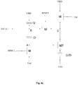
- Fig. 1 is a schematic diagram showing a structure of a pixel driving circuit according to an embodiment of the present disclosure.
- the pixel driving circuit according to the embodiment of the present disclosure can include: a compensating unit 11, a data writing unit 12, a driving unit 13, a first energy storage unit 14, a second energy storage unit 15 and a display unit 16.
- the compensating unit 11 is connected to a first level terminal, V1, a reset signal terminal, RESET, a control signal terminal, EM, a reference signal terminal, Vref, a first node, A, a second node, B and a third node, C.
- the compensating unit 11 is configured to write a level at the first level terminal V1 to the second node B and the third node C under control of the control signal terminal EM and the reset signal terminal RESET, and write a level at the reference signal terminal Vref to the first node A under control of the reset signal terminal RESET.
- the data writing unit 12 is connected to a scan signal terminal, SCAN, a data signal terminal, DATA, and the second node B, and is configured to write a signal at the data signal terminal DATA to the second node B under control of the scan signal terminal SCAN.
- the first energy storage unit 14 is connected to the first node A and the second node B, and is configured to store a voltage between the first node A and the second node B.
- the second energy storage unit 15 is connected to the first level terminal V1 and the second node B, and is configured to store a voltage between the first level terminal V1 and the second node B.
- the driving unit 13 is connected to the first node A, the third node C and the display unit 16, and is configured to output a driving signal to the display unit 16 under control of the first node A and the third node C.
- the display unit 16 is connected to the driving unit 13 and the second level terminal V2, and is configured to display grayscales under control of the driving signal 13 and the second level terminal V2.
- the compensating unit 11 writes the level at the first level terminal to the second node and the third node under control of the reset signal terminal and the control signal terminal, and writes the level at the reference signal terminal to the first node under control of the reset signal terminal.
- the second node is discharged via the driving unit and the display unit, and the first energy storage unit stores a threshold voltage of the driving unit.
- the data writing unit writes the signal at the data signal terminal to the second node under control of the scan signal terminal.
- the compensating unit writes the level at the first level terminal to the third node under control of the control signal terminal
- the second energy storage unit stores the voltage between the second node and the first level terminal
- the first energy storage unit stores the voltage between the second node and the first node
- the driving unit outputs the driving signal to the display unit
- the display unit displays grayscales under control of the driving signal and the second level terminal. Since the first energy storage unit stores the threshold voltage of the driving unit, in the light emission phase, the stored threshold voltage can be used directly to compensate for the threshold voltage of the driving unit.
- Fig. 2 is a schematic diagram showing an exemplary circuit structure of the pixel driving circuit shown in Fig. 1 .
- the compensating unit 11 of the pixel driving circuit includes a second transistor, M2, a third transistor, M3, and a fourth transistor, M4.
- the second transistor M2 has its gate connected to the reset signal terminal RESET, its first electrode connected to the third node C, and its second electrode connected to the second node B.
- the third transistor M3 has its gate connected to the control signal terminal EM, its first electrode connected to the first level terminal V1, and its second electrode connected to the third node C.
- the fourth transistor M4 has its gate connected to the reset signal terminal RESET, its first electrode connected to the reference signal terminal Vref, and its second electrode connected to the first node A.
- the data writing unit 12 can include: a first transistor M1 having its gate connected to the scan signal terminal SCAN, its first electrode connected to the data signal terminal DATA and its second electrode connected to the second node B.
- the driving unit 13 includes a driving transistor, MDT, having its gate connected to the first node A, its first electrode connected to the third node C and its second electrode connected to the display unit 16.
- MDT driving transistor
- the first energy storage unit 14 includes a first capacitor, C1, having its first terminal connected to the first node A and its second terminal connected to the second node B.
- the second energy storage unit 15 includes a second capacitor, C2, having its first terminal connected to the first level terminal V1 and its second terminal connected to the second node B.
- the display unit 16 includes an Organic Light Emitting Diode (OLED) having its first electrode connected to the driving unit 13 and its second electrode connected to the second level terminal V2.
- OLED Organic Light Emitting Diode
- the reset signal terminal controls the transistor M2, and the control signal terminal controls M3, to write the level at the first level terminal to the second node B and the third node C, and the reset signal terminal controls the transistor M4 to write the level at the reference signal terminal to the first node.
- the second node is discharged via the driving transistor MDT in the driving unit and the OLED in the display unit, and the capacitor C1 in the first energy storage unit stores the threshold voltage of the driving transistor MDT in the driving unit.
- the scan signal terminal in the data writing unit controls the transistor M1 to write the signal at the data signal terminal to the second node under.
- control signal terminal in the compensating unit controls the transistor M3 to write the level at the first level terminal to the third node
- the capacitor C2 in the second energy storage unit stores the voltage between the second node and the first level terminal
- the capacitor C1 in the first energy storage unit stores the voltage between the second node and the first node
- the MDT in the driving unit outputs the driving signal to the OLED in the display unit
- the OLED in the display unit displays grayscales under control of the driving signal and the second level terminal. Since the capacitor C1 in the first energy storage unit stores the threshold voltage of the MDT in the driving unit, in the light emission phase, the stored threshold voltage can be used directly to compensate for the threshold voltage of the MDT in the driving unit.
- the above transistors are all N-type or P-type transistors.
- P-type transistors are used.
- the light emitting device here can be an OLED.
- the first electrode of the OLED is anode
- the level V 2 at the second level terminal is lower than the level V 1 at the first level terminal.
- the low level is a ground terminal.
- Fig. 2 is described assuming the first electrode of the OLED to be anode.
- the driving method can include: a first phase in which the compensating unit writes a level at the first level terminal to the second node and the third node under control of the reset signal terminal and the control signal terminal and writes a level at the reference signal terminal to the first node under control of the reset signal terminal; a second phase in which the second node is discharged via the driving unit and the display unit, and the first energy storage unit stores a threshold voltage of the driving unit; a third phase in which the data writing unit writes a signal at the data signal terminal to the second node under control of the scan signal terminal; and a fourth phase in which the compensating unit writes the level at the first level terminal to the third node under control of the control signal terminal, the second energy storage unit stores a voltage between the second node and the first level terminal, the first energy storage unit stores a voltage between the second node and the first node, and driving unit outputs a driving signal
- the compensating unit includes a second transistor, a third transistor and a fourth transistor.
- the second transistor, the third transistor and the fourth transistor are all on, such that the level at the first level terminal is written to the third node via the third transistor and to the second node via the second transistor and the third transistor, and the level at the reference signal terminal is written to the first node via the fourth transistor.
- the second transistor and the fourth transistor are on, while the third transistor is off.
- the second transistor, the third transistor and the fourth transistor are all off.
- the second transistor and the fourth transistor are off, while the third transistor is on, such that the level at the first level terminal is written to the third node via the third transistor.
- the data writing unit includes a first transistor.
- the first transistor In the first phase, the first transistor is off. In the second phase, the first transistor is off. In the third phase, the first transistor is on, such that the signal at the data signal terminal is written to the second node via the first transistor. In the fourth phase, the first transistor is off.
- the transistors M1-M4 and the driving transistor DTFT are all P-type switching transistors.
- the terminal V1 is a high-level VDD signal and the terminal V2 is a low-level VSS signal.
- a driving method for the pixel driving circuit is provided according to an embodiment of the present disclosure.
- the working principles of the circuit can be divided into four parts, a first phase T1 of resetting, a second phase T2 of writing the threshold voltage to the driving transistor, a third phase T3 of writing the data signal, and the fourth phase T4 of light emitting.
- RESET and EM are low-voltage on signals and SCAN is a high-voltage off signal.
- RESET turns on the transistors M2 and M4. M2 being turned on allows the nodes B and C to be connected via M2. M4 being turned on allows the Vref signal at the Vref terminal to be written to the node A.
- EM turns on the transistor M3 and writes the VDD signal to the node C. Hence, the potentials at the nodes A and B of the capacitors C1 and C2 are reset to the potentials of Vref and VDD, respectively.
- RESET is a low-voltage on signal and SCAN and EM are high-voltage off signals.
- EM turns off M3, such that the VDD signal written in the phase T1 at the node B is discharged via the driving transistor MDT and the OLED, until the source potential of the driving transistor MDT is so low that the MDT is in a critical state before off or in an off state.
- the potential at the node B becomes Vref-Vth, where Vth is the threshold voltage of MDT.
- the voltages at the two terminals of the capacitor C1 are Vref at the node A and Vref-Vth at the node B, respectively.
- the capacitor C1 then maintains the threshold voltage of MDT at C1.
- the potential at the node B can be stored by the capacitor C2 and the potential VDD at the terminal V1. In this case, the charge at the node A can stored by the node B and C1 indirectly, so as to keep the potential at the node A in the light emitting phase the same as in the phase T3, i.e., Vdata +Vth.
- the working current I OLED is not influenced by the threshold voltage Vth and is dependent only on Vdata. In this way, the problem associated with the drifting threshold voltage of the driving transistor MDT due to manufacture process and long-term operation can be solved. Its influence on I OLED can be eliminated to ensure the normal function of the OLED.
- Fig. 5 shows current variations as the threshold voltage of the driving transistor MDT varies when the circuit structure is at high and low grayscales.
- the vertical axis denotes current different ratio and the horizontal axis denotes threshold voltage drifting.
- the threshold voltage drifting can be constrained to -0.3V to 0.3V.
- the threshold voltage drifting can be constrained to -0.3V to 0.3V.
- a display panel includes the above pixel driving circuit.
- a display apparatus includes the above display panel.
- the display apparatus can be an e-paper, a mobile phone, a television, a digital frame or any other display device.
- the display apparatus is capable of avoiding influence of a drifting threshold voltage of a driving transistor in a driving unit on a driving current of an active light emitting device by providing a compensating unit for compensating for the threshold voltage of the driving unit and thereby improving evenness of a displayed image.
Landscapes
- Engineering & Computer Science (AREA)
- Physics & Mathematics (AREA)
- Computer Hardware Design (AREA)
- General Physics & Mathematics (AREA)
- Theoretical Computer Science (AREA)
- Optics & Photonics (AREA)
- Control Of El Displays (AREA)
- Control Of Indicators Other Than Cathode Ray Tubes (AREA)
- Electroluminescent Light Sources (AREA)
Applications Claiming Priority (2)
| Application Number | Priority Date | Filing Date | Title |
|---|---|---|---|
| CN201510417355.5A CN104916257A (zh) | 2015-07-15 | 2015-07-15 | 一种像素电路及其驱动方法、显示面板和显示装置 |
| PCT/CN2016/070881 WO2017008484A1 (zh) | 2015-07-15 | 2016-01-14 | 一种像素驱动电路及其驱动方法、显示面板和显示装置 |
Publications (2)
| Publication Number | Publication Date |
|---|---|
| EP3188174A1 true EP3188174A1 (de) | 2017-07-05 |
| EP3188174A4 EP3188174A4 (de) | 2018-04-11 |
Family
ID=54085289
Family Applications (1)
| Application Number | Title | Priority Date | Filing Date |
|---|---|---|---|
| EP16823633.9A Withdrawn EP3188174A4 (de) | 2015-07-15 | 2016-01-14 | Pixelansteuerungsschaltung und ansteuerungsverfahren dafür sowie anzeigetafel und anzeigevorrichtung |
Country Status (4)
| Country | Link |
|---|---|
| US (1) | US10229639B2 (de) |
| EP (1) | EP3188174A4 (de) |
| CN (1) | CN104916257A (de) |
| WO (1) | WO2017008484A1 (de) |
Families Citing this family (29)
| Publication number | Priority date | Publication date | Assignee | Title |
|---|---|---|---|---|
| CN104916257A (zh) | 2015-07-15 | 2015-09-16 | 京东方科技集团股份有限公司 | 一种像素电路及其驱动方法、显示面板和显示装置 |
| CN105139804B (zh) * | 2015-09-28 | 2018-12-21 | 京东方科技集团股份有限公司 | 一种像素驱动电路、显示面板及其驱动方法和显示装置 |
| CN106935200A (zh) * | 2015-12-29 | 2017-07-07 | 上海和辉光电有限公司 | 有机发光显示装置及其驱动方法 |
| CN105427800B (zh) * | 2016-01-06 | 2018-06-12 | 京东方科技集团股份有限公司 | 像素电路、驱动方法、有机电致发光显示面板及显示装置 |
| CN106023898B (zh) * | 2016-07-26 | 2018-07-24 | 京东方科技集团股份有限公司 | 像素电路、显示面板及驱动方法 |
| US10431142B2 (en) | 2016-11-14 | 2019-10-01 | Int Tech Co., Ltd. | Pixel circuit and electroluminescent display comprising the pixel circuit |
| CN106652916B (zh) * | 2017-03-15 | 2019-01-15 | 京东方科技集团股份有限公司 | 像素驱动电路、显示装置及其显示方法 |
| CN109147665B (zh) * | 2017-06-16 | 2020-03-17 | 上海和辉光电有限公司 | 一种像素电路及其驱动方法、显示面板 |
| CN107464526B (zh) * | 2017-09-28 | 2020-02-18 | 京东方科技集团股份有限公司 | 一种像素补偿电路、其驱动方法及显示装置 |
| CN107767813A (zh) * | 2017-11-15 | 2018-03-06 | 武汉华星光电半导体显示技术有限公司 | 一种像素驱动电路及液晶显示装置 |
| CN108281112A (zh) * | 2018-02-05 | 2018-07-13 | 上海天马有机发光显示技术有限公司 | 像素驱动电路及其控制方法、显示面板和显示装置 |
| US10423286B1 (en) * | 2018-03-09 | 2019-09-24 | Int Tech Co., Ltd. | Circuit for fingerprint sensing and electronic device comprising the circuit |
| CN108492780A (zh) * | 2018-03-30 | 2018-09-04 | 京东方科技集团股份有限公司 | 像素电路及其驱动方法、阵列基板、显示装置 |
| TWI670706B (zh) * | 2018-05-24 | 2019-09-01 | 奕力科技股份有限公司 | 驅動電壓產生器 |
| CN110728946A (zh) * | 2018-06-29 | 2020-01-24 | 京东方科技集团股份有限公司 | 像素电路及其驱动方法、显示面板 |
| CN108962145B (zh) * | 2018-06-29 | 2021-03-23 | 北京大学深圳研究生院 | 显示装置及其像素电路和驱动方法 |
| CN108986748B (zh) * | 2018-08-02 | 2021-08-27 | 京东方科技集团股份有限公司 | 一种消除驱动晶体管漏电流的方法及系统、显示装置 |
| CN108962144B (zh) * | 2018-08-17 | 2020-06-19 | 京东方科技集团股份有限公司 | 一种像素驱动补偿电路、显示面板及驱动方法 |
| CN111243493B (zh) * | 2018-11-29 | 2022-07-08 | 成都辰显光电有限公司 | 一种像素电路、显示装置和像素电路的驱动方法 |
| CN113366562A (zh) * | 2019-07-12 | 2021-09-07 | 深圳市柔宇科技股份有限公司 | 像素单元、阵列基板与显示终端 |
| CN110620510B (zh) * | 2019-09-29 | 2020-07-28 | 维沃移动通信有限公司 | 电源电路、电子设备及电源电路控制方法 |
| KR102710277B1 (ko) * | 2019-11-12 | 2024-09-26 | 엘지디스플레이 주식회사 | 화소 구동 회로를 포함한 전계발광 표시패널 |
| KR102694938B1 (ko) * | 2019-12-30 | 2024-08-14 | 엘지디스플레이 주식회사 | 전계 발광 표시장치 |
| KR102811546B1 (ko) * | 2019-12-30 | 2025-05-21 | 엘지디스플레이 주식회사 | 화소회로, 발광표시장치 및 그의 구동방법 |
| CN113808542B (zh) * | 2021-09-22 | 2023-01-10 | 北京京东方技术开发有限公司 | 像素电路、驱动方法和显示装置 |
| CN113870786B (zh) * | 2021-09-28 | 2023-01-10 | 京东方科技集团股份有限公司 | 像素电路、驱动发光和显示装置 |
| CN116469338B (zh) * | 2022-01-11 | 2025-07-18 | 重庆康佳光电科技有限公司 | 一种像素驱动电路及其应用 |
| CN116312333B (zh) * | 2023-03-01 | 2024-05-14 | 昆山国显光电有限公司 | 像素电路及其驱动方法、显示面板 |
| CN119418669A (zh) * | 2025-01-02 | 2025-02-11 | 成都九天画芯科技有限公司 | 一种可实现Vth自补偿栅极控制电路及方法 |
Family Cites Families (18)
| Publication number | Priority date | Publication date | Assignee | Title |
|---|---|---|---|---|
| KR100673759B1 (ko) * | 2004-08-30 | 2007-01-24 | 삼성에스디아이 주식회사 | 발광 표시장치 |
| JP5017773B2 (ja) * | 2004-09-17 | 2012-09-05 | ソニー株式会社 | 画素回路及び表示装置とこれらの駆動方法 |
| JP4923410B2 (ja) * | 2005-02-02 | 2012-04-25 | ソニー株式会社 | 画素回路及び表示装置 |
| KR101152120B1 (ko) * | 2005-03-16 | 2012-06-15 | 삼성전자주식회사 | 표시 장치 및 그 구동 방법 |
| JP2008003544A (ja) | 2006-05-23 | 2008-01-10 | Sony Corp | 画像表示装置 |
| ITMI20070100A1 (it) * | 2007-01-24 | 2008-07-25 | St Microelectronics Srl | Circuito di pilotaggio di un diodo oled (diodo organico ed emissione di luce), in particolare per applicazione a display di tipo am-oled |
| KR101008482B1 (ko) | 2009-04-17 | 2011-01-14 | 삼성모바일디스플레이주식회사 | 화소 및 이를 이용한 유기전계발광 표시장치 |
| KR101073281B1 (ko) * | 2010-05-10 | 2011-10-12 | 삼성모바일디스플레이주식회사 | 유기전계발광 표시장치 및 그의 구동방법 |
| KR101859474B1 (ko) * | 2011-09-05 | 2018-05-23 | 엘지디스플레이 주식회사 | 유기 발광 다이오드 표시 장치의 화소 회로 |
| US9454932B2 (en) * | 2011-11-24 | 2016-09-27 | Joled Inc. | Display device and method of controlling the same |
| CN102982767B (zh) * | 2012-12-10 | 2015-02-25 | 京东方科技集团股份有限公司 | 一种像素单元驱动电路、驱动方法及显示装置 |
| TWI483233B (zh) * | 2013-02-08 | 2015-05-01 | Au Optronics Corp | 像素結構及其驅動方法 |
| CN103310732B (zh) * | 2013-06-09 | 2015-06-03 | 京东方科技集团股份有限公司 | 一种像素电路及其驱动方法、显示装置 |
| CN203288217U (zh) * | 2013-06-09 | 2013-11-13 | 京东方科技集团股份有限公司 | 一种像素电路及显示装置 |
| CN104200771B (zh) * | 2014-09-12 | 2017-03-01 | 上海天马有机发光显示技术有限公司 | 像素电路、阵列基板及显示装置 |
| CN104200777B (zh) * | 2014-09-25 | 2017-04-05 | 上海天马有机发光显示技术有限公司 | 像素电路及其驱动方法、显示面板、显示装置 |
| CN204808833U (zh) * | 2015-07-15 | 2015-11-25 | 京东方科技集团股份有限公司 | 一种像素电路、显示面板和显示装置 |
| CN104916257A (zh) * | 2015-07-15 | 2015-09-16 | 京东方科技集团股份有限公司 | 一种像素电路及其驱动方法、显示面板和显示装置 |
-
2015
- 2015-07-15 CN CN201510417355.5A patent/CN104916257A/zh active Pending
-
2016
- 2016-01-14 US US15/514,821 patent/US10229639B2/en active Active
- 2016-01-14 WO PCT/CN2016/070881 patent/WO2017008484A1/zh not_active Ceased
- 2016-01-14 EP EP16823633.9A patent/EP3188174A4/de not_active Withdrawn
Also Published As
| Publication number | Publication date |
|---|---|
| EP3188174A4 (de) | 2018-04-11 |
| CN104916257A (zh) | 2015-09-16 |
| WO2017008484A1 (zh) | 2017-01-19 |
| US10229639B2 (en) | 2019-03-12 |
| US20170229070A1 (en) | 2017-08-10 |
Similar Documents
| Publication | Publication Date | Title |
|---|---|---|
| US10229639B2 (en) | Pixel driving circuit for compensating drifting threshold voltage of driving circuit portion and driving method thereof | |
| EP3675100B1 (de) | Pixelschaltung und verfahren zum ansteuern derselben, anzeigevorrichtung | |
| US10825396B2 (en) | Pixel driving circuit and method for controlling the same, display driving circuit and method for controlling the same, and display panel | |
| US10923039B2 (en) | OLED pixel circuit and driving method thereof, and display device | |
| US10565933B2 (en) | Pixel circuit, driving method thereof, array substrate, display device | |
| CN104409047B (zh) | 像素驱动电路、像素驱动方法和显示装置 | |
| US10796625B2 (en) | Pixel circuit having dual-gate transistor, and driving method and display thereof | |
| US10078979B2 (en) | Display panel with pixel circuit having a plurality of light-emitting elements and driving method thereof | |
| EP3208793B1 (de) | Pixelschaltung und ansteuerungsverfahren dafür sowie organische lichtemittierende anzeige | |
| US9646540B2 (en) | Organic light emitting diode display device and method of driving the same | |
| US9898960B2 (en) | Pixel circuit, its driving method, OLED display panel and OLED display device | |
| US11127342B2 (en) | Pixel circuit for driving light emitting diode to emit light and method of controlling the pixel circuit | |
| US10504440B2 (en) | Pixel circuit, driving method thereof, display panel and display apparatus | |
| EP3257041B1 (de) | Pixelkompensationsschaltungen, zugehörige anzeigevorrichtung und verfahren zur ansteuerung davon | |
| CN104409043B (zh) | 像素驱动电路和像素驱动方法、显示装置 | |
| US9548024B2 (en) | Pixel driving circuit, driving method thereof and display apparatus | |
| US20170249898A1 (en) | Pixel circuit and driving method thereof, display substrate, and display apparatus | |
| JP5756859B2 (ja) | 画像表示装置 | |
| US9318048B2 (en) | Pixel circuit and display apparatus | |
| CN109166522B (zh) | 像素电路、其驱动方法及显示装置 | |
| US10424249B2 (en) | Pixel driving circuit and driving method thereof, array substrate, and display device | |
| US20190027091A9 (en) | Pixel circuit and method for driving pixel circuit | |
| US20170148389A1 (en) | Pixel Circuit | |
| US10796640B2 (en) | Pixel circuit, display panel, display apparatus and driving method | |
| JPWO2013021623A1 (ja) | 画像表示装置の駆動方法 |
Legal Events
| Date | Code | Title | Description |
|---|---|---|---|
| STAA | Information on the status of an ep patent application or granted ep patent |
Free format text: STATUS: THE INTERNATIONAL PUBLICATION HAS BEEN MADE |
|
| PUAI | Public reference made under article 153(3) epc to a published international application that has entered the european phase |
Free format text: ORIGINAL CODE: 0009012 |
|
| STAA | Information on the status of an ep patent application or granted ep patent |
Free format text: STATUS: REQUEST FOR EXAMINATION WAS MADE |
|
| 17P | Request for examination filed |
Effective date: 20170328 |
|
| AK | Designated contracting states |
Kind code of ref document: A1 Designated state(s): AL AT BE BG CH CY CZ DE DK EE ES FI FR GB GR HR HU IE IS IT LI LT LU LV MC MK MT NL NO PL PT RO RS SE SI SK SM TR |
|
| AX | Request for extension of the european patent |
Extension state: BA ME |
|
| A4 | Supplementary search report drawn up and despatched |
Effective date: 20180312 |
|
| RIC1 | Information provided on ipc code assigned before grant |
Ipc: G09G 3/3233 20160101AFI20180306BHEP Ipc: G09G 3/32 20160101ALI20180306BHEP |
|
| STAA | Information on the status of an ep patent application or granted ep patent |
Free format text: STATUS: THE APPLICATION HAS BEEN WITHDRAWN |
|
| 18W | Application withdrawn |
Effective date: 20180918 |
|
| DAV | Request for validation of the european patent (deleted) | ||
| DAX | Request for extension of the european patent (deleted) |