EP3185237B1 - Pixel circuit, organic electroluminescent display panel and display apparatus - Google Patents
Pixel circuit, organic electroluminescent display panel and display apparatus Download PDFInfo
- Publication number
- EP3185237B1 EP3185237B1 EP14884259.4A EP14884259A EP3185237B1 EP 3185237 B1 EP3185237 B1 EP 3185237B1 EP 14884259 A EP14884259 A EP 14884259A EP 3185237 B1 EP3185237 B1 EP 3185237B1
- Authority
- EP
- European Patent Office
- Prior art keywords
- terminal
- switching transistor
- signal
- module
- light emitting
- Prior art date
- Legal status (The legal status is an assumption and is not a legal conclusion. Google has not performed a legal analysis and makes no representation as to the accuracy of the status listed.)
- Active
Links
- 238000012360 testing method Methods 0.000 claims description 122
- 238000012545 processing Methods 0.000 claims description 20
- 239000003990 capacitor Substances 0.000 claims description 14
- 101100269674 Mus musculus Alyref2 gene Proteins 0.000 claims description 6
- 101100537098 Mus musculus Alyref gene Proteins 0.000 claims description 4
- 101150095908 apex1 gene Proteins 0.000 claims description 4
- 238000010586 diagram Methods 0.000 description 11
- 238000004519 manufacturing process Methods 0.000 description 5
- 230000000694 effects Effects 0.000 description 3
- 230000032683 aging Effects 0.000 description 2
- 230000008859 change Effects 0.000 description 2
- 238000013461 design Methods 0.000 description 2
- 241001508687 Mustela erminea Species 0.000 description 1
- 239000004973 liquid crystal related substance Substances 0.000 description 1
- 229910044991 metal oxide Inorganic materials 0.000 description 1
- 150000004706 metal oxides Chemical group 0.000 description 1
- 238000000034 method Methods 0.000 description 1
- 238000012544 monitoring process Methods 0.000 description 1
- 230000008569 process Effects 0.000 description 1
- 230000009467 reduction Effects 0.000 description 1
- 238000011160 research Methods 0.000 description 1
- 230000004044 response Effects 0.000 description 1
- 239000004065 semiconductor Substances 0.000 description 1
- 239000010409 thin film Substances 0.000 description 1
Images


Classifications
-
- G—PHYSICS
- G09—EDUCATION; CRYPTOGRAPHY; DISPLAY; ADVERTISING; SEALS
- G09G—ARRANGEMENTS OR CIRCUITS FOR CONTROL OF INDICATING DEVICES USING STATIC MEANS TO PRESENT VARIABLE INFORMATION
- G09G3/00—Control arrangements or circuits, of interest only in connection with visual indicators other than cathode-ray tubes
- G09G3/20—Control arrangements or circuits, of interest only in connection with visual indicators other than cathode-ray tubes for presentation of an assembly of a number of characters, e.g. a page, by composing the assembly by combination of individual elements arranged in a matrix no fixed position being assigned to or needed to be assigned to the individual characters or partial characters
- G09G3/22—Control arrangements or circuits, of interest only in connection with visual indicators other than cathode-ray tubes for presentation of an assembly of a number of characters, e.g. a page, by composing the assembly by combination of individual elements arranged in a matrix no fixed position being assigned to or needed to be assigned to the individual characters or partial characters using controlled light sources
- G09G3/30—Control arrangements or circuits, of interest only in connection with visual indicators other than cathode-ray tubes for presentation of an assembly of a number of characters, e.g. a page, by composing the assembly by combination of individual elements arranged in a matrix no fixed position being assigned to or needed to be assigned to the individual characters or partial characters using controlled light sources using electroluminescent panels
- G09G3/32—Control arrangements or circuits, of interest only in connection with visual indicators other than cathode-ray tubes for presentation of an assembly of a number of characters, e.g. a page, by composing the assembly by combination of individual elements arranged in a matrix no fixed position being assigned to or needed to be assigned to the individual characters or partial characters using controlled light sources using electroluminescent panels semiconductive, e.g. using light-emitting diodes [LED]
- G09G3/3208—Control arrangements or circuits, of interest only in connection with visual indicators other than cathode-ray tubes for presentation of an assembly of a number of characters, e.g. a page, by composing the assembly by combination of individual elements arranged in a matrix no fixed position being assigned to or needed to be assigned to the individual characters or partial characters using controlled light sources using electroluminescent panels semiconductive, e.g. using light-emitting diodes [LED] organic, e.g. using organic light-emitting diodes [OLED]
- G09G3/3225—Control arrangements or circuits, of interest only in connection with visual indicators other than cathode-ray tubes for presentation of an assembly of a number of characters, e.g. a page, by composing the assembly by combination of individual elements arranged in a matrix no fixed position being assigned to or needed to be assigned to the individual characters or partial characters using controlled light sources using electroluminescent panels semiconductive, e.g. using light-emitting diodes [LED] organic, e.g. using organic light-emitting diodes [OLED] using an active matrix
- G09G3/3233—Control arrangements or circuits, of interest only in connection with visual indicators other than cathode-ray tubes for presentation of an assembly of a number of characters, e.g. a page, by composing the assembly by combination of individual elements arranged in a matrix no fixed position being assigned to or needed to be assigned to the individual characters or partial characters using controlled light sources using electroluminescent panels semiconductive, e.g. using light-emitting diodes [LED] organic, e.g. using organic light-emitting diodes [OLED] using an active matrix with pixel circuitry controlling the current through the light-emitting element
-
- G—PHYSICS
- G09—EDUCATION; CRYPTOGRAPHY; DISPLAY; ADVERTISING; SEALS
- G09G—ARRANGEMENTS OR CIRCUITS FOR CONTROL OF INDICATING DEVICES USING STATIC MEANS TO PRESENT VARIABLE INFORMATION
- G09G3/00—Control arrangements or circuits, of interest only in connection with visual indicators other than cathode-ray tubes
- G09G3/006—Electronic inspection or testing of displays and display drivers, e.g. of LED or LCD displays
-
- G—PHYSICS
- G09—EDUCATION; CRYPTOGRAPHY; DISPLAY; ADVERTISING; SEALS
- G09G—ARRANGEMENTS OR CIRCUITS FOR CONTROL OF INDICATING DEVICES USING STATIC MEANS TO PRESENT VARIABLE INFORMATION
- G09G3/00—Control arrangements or circuits, of interest only in connection with visual indicators other than cathode-ray tubes
- G09G3/20—Control arrangements or circuits, of interest only in connection with visual indicators other than cathode-ray tubes for presentation of an assembly of a number of characters, e.g. a page, by composing the assembly by combination of individual elements arranged in a matrix no fixed position being assigned to or needed to be assigned to the individual characters or partial characters
- G09G3/22—Control arrangements or circuits, of interest only in connection with visual indicators other than cathode-ray tubes for presentation of an assembly of a number of characters, e.g. a page, by composing the assembly by combination of individual elements arranged in a matrix no fixed position being assigned to or needed to be assigned to the individual characters or partial characters using controlled light sources
- G09G3/30—Control arrangements or circuits, of interest only in connection with visual indicators other than cathode-ray tubes for presentation of an assembly of a number of characters, e.g. a page, by composing the assembly by combination of individual elements arranged in a matrix no fixed position being assigned to or needed to be assigned to the individual characters or partial characters using controlled light sources using electroluminescent panels
- G09G3/32—Control arrangements or circuits, of interest only in connection with visual indicators other than cathode-ray tubes for presentation of an assembly of a number of characters, e.g. a page, by composing the assembly by combination of individual elements arranged in a matrix no fixed position being assigned to or needed to be assigned to the individual characters or partial characters using controlled light sources using electroluminescent panels semiconductive, e.g. using light-emitting diodes [LED]
- G09G3/3208—Control arrangements or circuits, of interest only in connection with visual indicators other than cathode-ray tubes for presentation of an assembly of a number of characters, e.g. a page, by composing the assembly by combination of individual elements arranged in a matrix no fixed position being assigned to or needed to be assigned to the individual characters or partial characters using controlled light sources using electroluminescent panels semiconductive, e.g. using light-emitting diodes [LED] organic, e.g. using organic light-emitting diodes [OLED]
- G09G3/3225—Control arrangements or circuits, of interest only in connection with visual indicators other than cathode-ray tubes for presentation of an assembly of a number of characters, e.g. a page, by composing the assembly by combination of individual elements arranged in a matrix no fixed position being assigned to or needed to be assigned to the individual characters or partial characters using controlled light sources using electroluminescent panels semiconductive, e.g. using light-emitting diodes [LED] organic, e.g. using organic light-emitting diodes [OLED] using an active matrix
- G09G3/3258—Control arrangements or circuits, of interest only in connection with visual indicators other than cathode-ray tubes for presentation of an assembly of a number of characters, e.g. a page, by composing the assembly by combination of individual elements arranged in a matrix no fixed position being assigned to or needed to be assigned to the individual characters or partial characters using controlled light sources using electroluminescent panels semiconductive, e.g. using light-emitting diodes [LED] organic, e.g. using organic light-emitting diodes [OLED] using an active matrix with pixel circuitry controlling the voltage across the light-emitting element
-
- G—PHYSICS
- G09—EDUCATION; CRYPTOGRAPHY; DISPLAY; ADVERTISING; SEALS
- G09G—ARRANGEMENTS OR CIRCUITS FOR CONTROL OF INDICATING DEVICES USING STATIC MEANS TO PRESENT VARIABLE INFORMATION
- G09G2310/00—Command of the display device
- G09G2310/02—Addressing, scanning or driving the display screen or processing steps related thereto
- G09G2310/0243—Details of the generation of driving signals
- G09G2310/0251—Precharge or discharge of pixel before applying new pixel voltage
-
- G—PHYSICS
- G09—EDUCATION; CRYPTOGRAPHY; DISPLAY; ADVERTISING; SEALS
- G09G—ARRANGEMENTS OR CIRCUITS FOR CONTROL OF INDICATING DEVICES USING STATIC MEANS TO PRESENT VARIABLE INFORMATION
- G09G2320/00—Control of display operating conditions
- G09G2320/02—Improving the quality of display appearance
- G09G2320/0233—Improving the luminance or brightness uniformity across the screen
-
- G—PHYSICS
- G09—EDUCATION; CRYPTOGRAPHY; DISPLAY; ADVERTISING; SEALS
- G09G—ARRANGEMENTS OR CIRCUITS FOR CONTROL OF INDICATING DEVICES USING STATIC MEANS TO PRESENT VARIABLE INFORMATION
- G09G2320/00—Control of display operating conditions
- G09G2320/02—Improving the quality of display appearance
- G09G2320/029—Improving the quality of display appearance by monitoring one or more pixels in the display panel, e.g. by monitoring a fixed reference pixel
- G09G2320/0295—Improving the quality of display appearance by monitoring one or more pixels in the display panel, e.g. by monitoring a fixed reference pixel by monitoring each display pixel
-
- G—PHYSICS
- G09—EDUCATION; CRYPTOGRAPHY; DISPLAY; ADVERTISING; SEALS
- G09G—ARRANGEMENTS OR CIRCUITS FOR CONTROL OF INDICATING DEVICES USING STATIC MEANS TO PRESENT VARIABLE INFORMATION
- G09G2320/00—Control of display operating conditions
- G09G2320/06—Adjustment of display parameters
- G09G2320/0626—Adjustment of display parameters for control of overall brightness
-
- G—PHYSICS
- G09—EDUCATION; CRYPTOGRAPHY; DISPLAY; ADVERTISING; SEALS
- G09G—ARRANGEMENTS OR CIRCUITS FOR CONTROL OF INDICATING DEVICES USING STATIC MEANS TO PRESENT VARIABLE INFORMATION
- G09G2330/00—Aspects of power supply; Aspects of display protection and defect management
- G09G2330/12—Test circuits or failure detection circuits included in a display system, as permanent part thereof
Definitions
- the present disclosure relates to a pixel circuit, an organic light emitting display panel and display apparatus.
- OLED organic light emitting display
- LCD liquid crystal display
- advantages of low power consumption, low production cost, self-luminescent, broad view angle and fast response speed and so on At present, in the display field such as mobile phone, PDA and digital camera and the like, OLED has taken the place of the traditional LCD display screen. Unlike that LCD controls luminance by using a stable voltage, OLED is current-driven and a stable current is required to control light emitting.
- US 2010/079361 A1 discloses a pixel of a display device wherein a first transistor of which a second terminal is connected to a first terminal of a light emitting element supplies a driving current that corresponds to a voltage between a control terminal and the second terminal to the light emitting elements, and a second terminal of the light emitting element is connected to a driving voltage.
- At least one second transistor transmits a black voltage that corresponds to a black gray to the control terminal of the first transistor in a first period and a second period, and transmits a gray voltage that corresponds to an input image signal to the control terminal of the first transistor in a third period.
- a third transistor is connected between the first terminal of the light emitting element and a voltage supply line to transmit a reference voltage, and the third transistor is turned on in the first period and turned off in the second period.
- a capacitor between the control terminal and the source of the first transistor stores a control voltage based on a threshold voltage of the first transistor in the second period, and stores a voltage based on the control voltage and the gray voltage in the third period.
- Document US20130050292A1 discloses an OLED circuit with a monitoring of the OLED anode via an additional transistor connected to the data line.
- a pixel circuit, an organic light emitting display panel and a display apparatus which are used to solve the problem existing in the prior art that a current for driving a light emitting device OLED in the display apparatus has poor uniformity and display luminance is non-uniform.
- the invention is defined in claim 1.
- the testing module can comprise: a first switching transistor, and a second switching transistor and a third switching transistor which have a same doping polarity; and the first switching transistor has a doping polarity inverse to the second switching transistor and the third switching transistor respectively;
- the charging module can comprise a fourth switching transistor; wherein a gate of the fourth switching transistor is connected to the scan signal, a source of the fourth switching transistor is connected to the data signal, and a drain of the fourth switching transistor is connected to the first terminal and the third terminal of the testing module.
- the driving module can comprise: a storage capacitor and a fifth switching transistor;
- an organic light emitting display panel comprising a plurality of the pixel circuits provided in the embodiment of the present disclosure arranged in array.
- a display apparatus comprising the organic light emitting display panel provided in the embodiment of the present disclosure.
- the display apparatus in the embodiment of the present disclosure, it is further comprised: a test controlling unit connected to a test signal terminal through a test signal line, and a compensation processing unit and a driving unit connected to a data signal terminal through a data line;
- the compensation processing unit and the driving unit are integrated on a same chip.
- a testing module is added to the pixel circuit.
- the testing module receives the test signal switching between the displaying period of time and the testing period of time, and is configured to connect the second terminal of the charging module with the control terminal of the driving module during the displaying period of time and connect the second reference signal terminal with the second terminal of the light emitting device, so that the charging module provides the driving voltage signal to the driving module under the control of the scan signal terminal, and the driving module drives the light emitting device to emit light under the control of the driving voltage signal, thereby realizing the function of emitting light normally.
- This testing module is further configured to connect the second terminal of the light emitting device with the output ermine of the charging module during the testing period of time, so that the charging module outputs the current signal of the light emitting device to the data signal terminal under the control of the scan signal terminal, and then an external compensation processing unit determines the compensation voltage signal for the respective pixel circuits according to the current signal received by the data signal terminal, and the driving unit transmits the compensation voltage signal determined by the compensation processing unit and the data signal received from the signal source to the data signal terminal after superposing them.
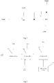
- Fig.1 is a schematic diagram of a configuration of a known pixel circuit.
- the pixel circuit driving OLED to emit light comprises: a driving transistor M1, a second switching transistor M2, a storage capacitor C and a light emitting device OLED; wherein a gate of the driving transistor M1 is connected to a drain of the second switching transistor M2 and one terminal of the storage capacitor C respectively, a source thereof is connected to the other terminal of the storage capacitor C and a high voltage signal terminal VDD, and a drain thereof is connected to one terminal of the light emitting device OLED; a gate of the switching transistor M2 is connected to a scan signal terminal Gate, and a drain thereof is connected to a data signal terminal Data; the other terminal of the light I emitting device OLED is connected to a low voltage signal terminal VSS.
- the driving transistor M1 drives the light emitting device OLED to emit light
- a driving current is controlled by the high voltage signal terminal VDD, the data signal terminal Data and the driving transistor M1 jointly.
- the driving transistor M1 cannot be made completely consistent in the manufacturing process thereof, and non-uniformity exists in a threshold voltage V th of the driving transistor M1 in the respective pixel circuits due to manufacturing process and device aging and so on, which result in a change occurring in a current flowing through OLED of each pixel point, so that the display luminance is non-uniform, thereby influencing the display effect of the entire image.
- Fig.2 shows a schematic diagram of a configuration of a pixel circuit provided in an embodiment of the present disclosure.
- the pixel circuit in the embodiment of the present disclosure comprises: a light emitting device 01, a charging module 02, a driving module 03, and a testing module 04.
- a first terminal of the charging module 02 is connected to the data signal terminal Data
- a control terminal thereof is connected to the scan signal terminal Gate
- a second terminal thereof is connected to a first terminal a1 and a third terminal b1 of the testing module 04 respectively.
- a control terminal of the driving module 03 is connected to a fourth terminal b2 of the testing module 04, an input terminal thereof is connected to a first reference signal terminal Ref1, and an output terminal thereof is connected to a first terminal of the light emitting device 01.
- a control terminal of the testing module 04 is connected to a test signal terminal TEST, a second terminal a2 thereof is connected to a second terminal of the light emitting device 01, and a fifth terminal b3 thereof is connected to a second reference signal terminal Ref2; the test signal terminal TEST is used to provide a test signal switching between a displaying period of time and a testing period of time.
- the testing module 04 is configured to connect the second terminal of the charging module 02 with the control terminal of the driving module 03 and connect the second reference signal terminal Ref2 with the second terminal of the light emitting device 01, so that the charging module 02 provides a driving voltage signal to the driving module 03 under the control of the scan signal terminal Gate, and the driving module 03 drives the light emitting device 01 to emit light under the control of the driving voltage signal.
- the testing module 04 is configured to connect the second terminal of the light emitting device 01 with the second terminal of the charging module 02, so that the charging module 02 outputs a current signal of the light emitting device 01 to the data signal terminal Data under the control of the scan signal terminal Gate.
- a testing module 04 is added.
- the testing module 04 receives the test signal switching between the displaying period of time and the testing period of time, and is configured to connect the second terminal of the charging module 02 with the control terminal of the driving module 03 during the displaying period of time, and connect the second reference signal terminal Ref2 with the second terminal of the light emitting device 01, so that the charging module 02 provides the driving voltage signal to the driving module 03 under the control of the scan signal terminal Gate, and the driving module 03 drives the light emitting device 01 to emit light under the control of the driving voltage signal, thereby realizing the function of emitting light normally.
- the testing module 04 is further configured to connect the second terminal of the light emitting device 01 with the second terminal of the charging module 02 during the testing period of time, so that the charging module 02 outputs the current signal of the light emitting device 01 to the data signal terminal Data under the control of the scan signal terminal Gate, which provides a flowing path for the current signal of the light emitting device 01 to flow into the data signal terminal Data to complete the testing.
- the current signal for driving the light emitting device in each pixel achieves the uniformity standard, so that the display luminance of each pixel is uniform, thereby ensuring the quality of the display picture.
- the testing module 04 in the pixel circuit provided in the embodiment of the present disclosure can comprise: a first switching transistor T1, and a second switching transistor T2 and a third switching transistor T3 which have the same doping polarity; the first switching transistor T1 has a doping polarity inverse to the second switching transistor T2 and the third switching transistor T3.
- a gate of the first switching transistor T1, a gate of the second switching transistor T2 and a gate of the third switching transistor T3 are connected to the test signal terminal TEST respectively;
- the testing module 04 when the testing module 04 is composed by adopting the first switching transistor T1, the second switching transistor T2 and the third switching transistor T3, by combining with the operation timing diagrams as shown in Figs.3b and 4b , where Figs.3b and 4b are specific to scan pixel circuits of one row, it has the following operating principle: during a displaying period of time A, the test signal terminal TEST is inputted a test signal to control the first switching transistor T1 to be in a turn-off state and control the second switching transistor T2 and the third switching transistor T3 to be in a turn-on state, so that the charging module 02 outputs the driving voltage signal to the driving module 03, and the driving module 03 drives the light emitting device 01 to emit light under the control of the driving voltage signal.
- the test signal terminal TEST is inputted a test signal having a polarity inverse to the test signal inputted during the displaying period of time A to control the first switching transistor T1 to be in the turn-on state and control the second switching transistor T2 and the third switching transistor T3 to be in the turn-off state, so that the current signal of the light-emitting device 01 flows into the second terminal of the charging module 02, and the charging module 02 outputs the current signal of the light emitting device 01 to the data signal terminal Data under the control of the scan signal terminal Gate, that is, current flowing directions in the pixel circuit during the displaying period of time A and the testing period of time B are inverse to each other to provide the flowing path of the current signal in order to complete the testing of the driving current signal and the external compensation, , which finally realizes that the current signal for driving the light emitting device 01 in each pixel achieves the uniformity standard, so that the display luminance of each pixel is uniform, thereby ensuring the quality of the display picture.
- the testing module 04 has to complete different operations during the displaying period of time A and the testing period of time B, and thus it requires that the first switching transistor T1 has a doping type inverse to the second switching transistor T2 and the third switching transistor T3 respectively.
- the first switching transistor T1 can be set as an N type transistor, while the second switching transistor T2 and the third switching transistor T3 can be set as P type transistors.
- the test signal terminal TEST is inputted a low level signal during the displaying period of time A to control the first switching transistor T1 to be in the turn-off state and control the second switching transistor T2 and the third switching transistor T3 to be in the turn-on state, and that the test signal terminal TEST is inputted a high level signal during the testing period of time B to control the first switching transistor T1 to be in the turn-on state and control the second switching transistor T2 and the third switching transistor T3 to be in the turn-off state.
- the first switching transistor T1 is set as the P type transistor
- the second switching transistor T2 and the third switching transistor T3 are set as the N type transistor.
- the test signal terminal TEST is inputted the high level signal during the displaying period of time A to control the first switching transistor T1 to be in the turn-off state and control the second switching transistor T2 and the third switching transistor T3 to be in the turn-on state, and that the test signal terminal TEST is inputted the low level signal during the testing period of time B to control the first switching transistor T1 to be in the turn-on state and control the second switching transistor T2 and the third switching transistor T3 to be in the turn-off state.
- the first switching transistor T1, the second switching transistor T2 and the third switching transistor T3 are turned on at different times under the control of the test signal terminal TEST to complete functions of the testing module 04 during different periods of time.
- the charging module 02 can comprise: a fourth switching transistor T4, whose gate is connected to the scan signal terminal Gate, source is connected to the data signal terminal Data, and drain is connected to the first terminal a1 and the third terminal b1 of the testing module 04.
- the fourth switching transistor T4 can be the P type transistor as shown in Fig.3a .
- the fourth switching transistor T4 can be the N type transistor as shown in Fig.4a , to which no limitation is made herein.
- the scan signal terminal Gate is inputted the low level signal to control the fourth switching transistor T4 to be in the turn-on state, and the turned-on fourth switching transistor T4 outputs the driving voltage signal of the data signal terminal Data to the control terminal of the driving module 03 through the testing module 04, so that the driving module 03 drives the light emitting device 01 to emit light under the control of the driving voltage signal, thereby realizing the function of emitting light normally;
- the scan signal terminal Gate is still inputted the low level signal to control the fourth switching transistor T4 to be in the turn-on state, and the turned on fourth switching transistor T4 outputs the current signal of the light emitting device 01 outputted by the testing module 04 to the data signal terminal Data, which provides the flowing path for the current signal of the light emitting device 01 to flow into the data signal terminal Data to complete the testing.
- the scan signal terminal Gate is inputted the high level signal to control the fourth switching transistor T4 to be in the turn-on state, and the function completed by the turned on fourth switching transistor T4 during the displaying period of time A and the testing period of time B is the same as that completed by the fourth switching transistor T4 when it is manufactured by adopting the P type transistor.
- the repeated description is not given herein.
- the driving module 03 can comprise: a storage capacitor C1 and a fifth switching transistor T5; a source of the fifth switching transistor T5 is connected to the first reference signal terminal Ref1, a gate thereof is connected to the fourth terminal b2 of the testing module 04, and a drain thereof is connected to the first terminal of the light emitting device 01; when the fifth switching transistor T5 is the P type transistor, the storage capacitor C1 is connected in parallel between the source and the gate of the fifth switching transistor T5; when the fifth switching transistor T5 is the N type transistor, the storage capacitor C1 is connected in parallel between the drain and the gate of the fifth switching transistor T5.
- the fifth switching transistor T5 drives the light emitting device 01 to emit light under the control of the driving voltage signal; during the testing period of time B, since the storage capacitor C1 is discharged to provide the driving voltage signal to the fifth switching transistor T5, the fifth switching transistor T5 is still in the turn-on state and drives the light emitting device 01 to emit light continuously.
- the switching transistors described in the embodiment of the present disclosure can be thin film transistors (TFT) or can be metal oxide semiconductors (MOS), to which no limitation is made herein.
- TFT thin film transistors
- MOS metal oxide semiconductors
- sources and drains of these transistors can be exchanged with each other, and no specific distinction is made between these sources and drains.
- the pixel circuit provided in the embodiment of the present disclosure can realize the function of external compensation, or can be applicable to a pixel circuit having the function of internal compensation, so that compensation for the threshold voltage of the driving transistor is realized. Its implementation and operating principle are similar to the above pixel circuit provided in the embodiments of the present disclosure, and thus the repeated description is not given herein.
- an organic light emitting display panel comprising a plurality of pixel circuits provided in the embodiment of the present disclosure arranged in array. Since the organic light emitting display panel has a principle for solving the problem similar to the pixel circuit, the implementation of the organic light emitting display panel can refer to the implementation of the pixel circuit. Thus, the repeated description is not further given herein.
- a display apparatus comprising the organic light emitting display panel provided in the embodiment of the present disclosure.
- the display apparatus can be any product or components having the displaying function, such as a mobile phone, a tablet computer, a TV set, a display device, a notebook computer, a digital photo frame, and a navigator and so on. Since the display apparatus has a principle for solving the problem similar to the organic light emitting display panel, the implementation of the display apparatus can refer to the implementation of the organic light emitting display panel. Thus, the repeated description is not further given herein.
- Fig.5 shows a schematic diagram of a configuration of the display apparatus provided in the embodiment of the present disclosure.
- the display apparatus provided in the embodiment of the present disclosure can further comprise:
- the charging module 02 in the pixel circuit provides the driving voltage signal to the driving module 03 through the testing module 04 to control the driving module 03 to drive the light emitting device 01 to emit light, thereby realizing the function of emitting light normally; during the testing period of time, the current signal outputted by the second terminal of the light emitting device 01 flows through the testing module 04 to reach the second terminal of the charging module 02, and the charging module 02 outputs the current signal to the data signal terminal Data under the control of the scan signal terminal Gate, so that the compensation processing unit 06 determines the compensation voltage signal for the respective pixel circuits according to the current signal received from the data signal terminal Data, and the driving unit 07 superpose the compensation voltage signal determined by the compensation processing unit 06 and the data signal received from the signal source and then transmit them to the data signal terminal Data, thereby realizing the function of compensating.
- the compensation processing unit 06 is used, by combining with the gating effect of the scan signal terminal Gate, to determine a corresponding compensation voltage signal according to the current signal received by the data signal terminal Data of each pixel unit, and for the pixel unit whose compensation voltage signal is determined, external compensation is realized through the driving unit 07, and then the current of each pixel unit is tested again until the current of all the pixel units reaches the uniformity standard.
- a compensation parameter is written into the driving unit 07, for example, the pixel units in the N-th column and the N-th row need a compensation voltage signal of -0.1V, then in the subsequent pixel driving process, the driving voltage signal of the pixel unit is maintained a reduction of 0.1V. In this way, the driving current of the respective pixel units reaching the uniformity standard is finally realized, and the uniformity of the display luminance of pixels is ensured, so that the quality of the display picture is ensured.
- the compensation processing unit 06 and the driving unit 07 can be integrated on a same chip.
- the test controlling unit 05, the compensation processing unit 06 and the driving unit 07 can also be integrated on the same chip.
- Such a design is advantageous for realizing a simultaneous control of all the pixels by using the smallest occupation space, to avoid that an aperture ratio of the product is affected, the arrangement space is saved, and the production cost is reduced.
- a testing module is added to the pixel circuit.
- the testing module receives the test signal switching between the displaying period of time and the testing period of time, and is configured to connect the second terminal of the charging module with the control terminal of the driving module during the displaying period of time, and connect the second reference signal terminal with the second terminal of the light emitting device, so that the charging module provides the driving voltage signal to the driving module under the control of the scan signal terminal, and the driving module drives the light emitting device to emit light under the control of the driving voltage signal, thereby realizing the function of emitting light normally.
- the testing module is further configured to connect the second terminal of the light emitting device with the second terminal of the charging module during the testing period of time, so that the charging module outputs the current signal of the light emitting device to the data signal terminal under the control of the scan signal terminal, and then the external compensation processing unit determines the compensation voltage signal for the respective pixel circuits according to the current signal received by the data signal terminal, and the driving unit superpose the compensation voltage signal determined by the compensation processing unit and the data signal received from the signal source and then transmit the superposed signals to the data signal terminal.
- the external compensation function is realized, and the current signal for driving the light emitting device in each pixel achieving the uniformity standard is finally realized, so that display luminance of each pixel is uniform, thereby ensuring the quality of the display picture.
Landscapes
- Engineering & Computer Science (AREA)
- Physics & Mathematics (AREA)
- Computer Hardware Design (AREA)
- General Physics & Mathematics (AREA)
- Theoretical Computer Science (AREA)
- Control Of Indicators Other Than Cathode Ray Tubes (AREA)
- Control Of El Displays (AREA)
- Electroluminescent Light Sources (AREA)
Applications Claiming Priority (2)
| Application Number | Priority Date | Filing Date | Title |
|---|---|---|---|
| CN201410419203.4A CN104240639B (zh) | 2014-08-22 | 2014-08-22 | 一种像素电路、有机电致发光显示面板及显示装置 |
| PCT/CN2014/090625 WO2016026218A1 (zh) | 2014-08-22 | 2014-11-07 | 像素电路、有机电致发光显示面板及显示装置 |
Publications (3)
| Publication Number | Publication Date |
|---|---|
| EP3185237A1 EP3185237A1 (en) | 2017-06-28 |
| EP3185237A4 EP3185237A4 (en) | 2018-03-21 |
| EP3185237B1 true EP3185237B1 (en) | 2021-10-27 |
Family
ID=52228612
Family Applications (1)
| Application Number | Title | Priority Date | Filing Date |
|---|---|---|---|
| EP14884259.4A Active EP3185237B1 (en) | 2014-08-22 | 2014-11-07 | Pixel circuit, organic electroluminescent display panel and display apparatus |
Country Status (4)
| Country | Link |
|---|---|
| US (1) | US9711085B2 (zh) |
| EP (1) | EP3185237B1 (zh) |
| CN (1) | CN104240639B (zh) |
| WO (1) | WO2016026218A1 (zh) |
Families Citing this family (43)
| Publication number | Priority date | Publication date | Assignee | Title |
|---|---|---|---|---|
| US10012678B2 (en) | 2004-12-15 | 2018-07-03 | Ignis Innovation Inc. | Method and system for programming, calibrating and/or compensating, and driving an LED display |
| US8576217B2 (en) | 2011-05-20 | 2013-11-05 | Ignis Innovation Inc. | System and methods for extraction of threshold and mobility parameters in AMOLED displays |
| US9799246B2 (en) | 2011-05-20 | 2017-10-24 | Ignis Innovation Inc. | System and methods for extraction of threshold and mobility parameters in AMOLED displays |
| US10013907B2 (en) | 2004-12-15 | 2018-07-03 | Ignis Innovation Inc. | Method and system for programming, calibrating and/or compensating, and driving an LED display |
| KR20070101275A (ko) | 2004-12-15 | 2007-10-16 | 이그니스 이노베이션 인크. | 발광 소자를 프로그래밍하고, 교정하고, 구동시키기 위한방법 및 시스템 |
| EP1904995A4 (en) | 2005-06-08 | 2011-01-05 | Ignis Innovation Inc | METHOD AND SYSTEM FOR CONTROLLING A LIGHT EMITTING DEVICE DISPLAY |
| EP2008264B1 (en) | 2006-04-19 | 2016-11-16 | Ignis Innovation Inc. | Stable driving scheme for active matrix displays |
| CA2556961A1 (en) | 2006-08-15 | 2008-02-15 | Ignis Innovation Inc. | Oled compensation technique based on oled capacitance |
| US9384698B2 (en) | 2009-11-30 | 2016-07-05 | Ignis Innovation Inc. | System and methods for aging compensation in AMOLED displays |
| US9311859B2 (en) | 2009-11-30 | 2016-04-12 | Ignis Innovation Inc. | Resetting cycle for aging compensation in AMOLED displays |
| US10319307B2 (en) | 2009-06-16 | 2019-06-11 | Ignis Innovation Inc. | Display system with compensation techniques and/or shared level resources |
| CA2692097A1 (en) | 2010-02-04 | 2011-08-04 | Ignis Innovation Inc. | Extracting correlation curves for light emitting device |
| US9881532B2 (en) | 2010-02-04 | 2018-01-30 | Ignis Innovation Inc. | System and method for extracting correlation curves for an organic light emitting device |
| US20140313111A1 (en) | 2010-02-04 | 2014-10-23 | Ignis Innovation Inc. | System and methods for extracting correlation curves for an organic light emitting device |
| US10089921B2 (en) | 2010-02-04 | 2018-10-02 | Ignis Innovation Inc. | System and methods for extracting correlation curves for an organic light emitting device |
| US9530349B2 (en) | 2011-05-20 | 2016-12-27 | Ignis Innovations Inc. | Charged-based compensation and parameter extraction in AMOLED displays |
| US9466240B2 (en) | 2011-05-26 | 2016-10-11 | Ignis Innovation Inc. | Adaptive feedback system for compensating for aging pixel areas with enhanced estimation speed |
| JP2014517940A (ja) | 2011-05-27 | 2014-07-24 | イグニス・イノベイション・インコーポレーテッド | Amoledディスプレイにおけるエージング補償ためのシステムおよび方法 |
| US10089924B2 (en) | 2011-11-29 | 2018-10-02 | Ignis Innovation Inc. | Structural and low-frequency non-uniformity compensation |
| US9324268B2 (en) | 2013-03-15 | 2016-04-26 | Ignis Innovation Inc. | Amoled displays with multiple readout circuits |
| US8937632B2 (en) | 2012-02-03 | 2015-01-20 | Ignis Innovation Inc. | Driving system for active-matrix displays |
| US8922544B2 (en) | 2012-05-23 | 2014-12-30 | Ignis Innovation Inc. | Display systems with compensation for line propagation delay |
| EP3043338A1 (en) | 2013-03-14 | 2016-07-13 | Ignis Innovation Inc. | Re-interpolation with edge detection for extracting an aging pattern for amoled displays |
| US9761170B2 (en) | 2013-12-06 | 2017-09-12 | Ignis Innovation Inc. | Correction for localized phenomena in an image array |
| US9502653B2 (en) | 2013-12-25 | 2016-11-22 | Ignis Innovation Inc. | Electrode contacts |
| CA2879462A1 (en) | 2015-01-23 | 2016-07-23 | Ignis Innovation Inc. | Compensation for color variation in emissive devices |
| CN104680979B (zh) * | 2015-03-23 | 2019-03-12 | 京东方科技集团股份有限公司 | Oled显示装置和用于矫正oled显示装置的残像的方法 |
| CA2889870A1 (en) | 2015-05-04 | 2016-11-04 | Ignis Innovation Inc. | Optical feedback system |
| CA2892714A1 (en) | 2015-05-27 | 2016-11-27 | Ignis Innovation Inc | Memory bandwidth reduction in compensation system |
| CA2900170A1 (en) | 2015-08-07 | 2017-02-07 | Gholamreza Chaji | Calibration of pixel based on improved reference values |
| CN105185321B (zh) * | 2015-10-27 | 2018-05-29 | 深圳市华星光电技术有限公司 | Amoled驱动电路、显示面板及显示器 |
| WO2017094461A1 (ja) * | 2015-12-01 | 2017-06-08 | シャープ株式会社 | 画像形成素子 |
| CN106328060B (zh) * | 2016-09-07 | 2019-02-12 | 深圳市华星光电技术有限公司 | 一种amoled面板及该面板像素驱动电路的漂移补偿方法 |
| CN108120915B (zh) * | 2017-12-15 | 2020-05-05 | 京东方科技集团股份有限公司 | 应用于显示面板的老化处理方法及老化处理系统 |
| CN108470534B (zh) * | 2018-05-25 | 2023-08-04 | 南京微芯华谱信息科技有限公司 | 应用于自发光的像素单元电路、测试电路及测试方法 |
| TWI676979B (zh) * | 2018-11-20 | 2019-11-11 | 友達光電股份有限公司 | 顯示面板及顯示面板的檢測方法 |
| CN109473064B (zh) * | 2018-12-14 | 2020-06-09 | 京东方科技集团股份有限公司 | 电压补偿方法及装置、显示装置 |
| CN110570809B (zh) * | 2019-09-10 | 2021-04-16 | 成都辰显光电有限公司 | 一种显示面板和显示面板的测试方法 |
| CN110890065B (zh) * | 2019-11-01 | 2021-04-27 | 深圳市华星光电半导体显示技术有限公司 | 显示面板的控制方法及控制装置 |
| CN112634800A (zh) * | 2020-12-22 | 2021-04-09 | 北方液晶工程研究开发中心 | 快速自动测试发光二极管显示屏刷新频率的方法及系统 |
| CN113345355B (zh) * | 2021-06-09 | 2022-08-23 | 云谷(固安)科技有限公司 | 显示面板的Mura检测方法、装置及介质 |
| CN115547243B (zh) * | 2022-09-20 | 2024-07-02 | 上海天马微电子有限公司 | 发光面板及其驱动方法、显示装置 |
| CN115631726B (zh) * | 2022-12-21 | 2023-03-10 | 惠科股份有限公司 | 阵列基板和显示面板 |
Family Cites Families (17)
| Publication number | Priority date | Publication date | Assignee | Title |
|---|---|---|---|---|
| JP2006106122A (ja) * | 2004-09-30 | 2006-04-20 | Toshiba Corp | 映像表示装置 |
| TWI317926B (en) * | 2005-12-20 | 2009-12-01 | Au Optronics Corp | Electroluminescent display panel testing apparatus and method thereof |
| JP5240542B2 (ja) * | 2006-09-25 | 2013-07-17 | カシオ計算機株式会社 | 表示駆動装置及びその駆動方法、並びに、表示装置及びその駆動方法 |
| JP2008257086A (ja) * | 2007-04-09 | 2008-10-23 | Sony Corp | 表示装置、表示装置の製造方法および電子機器 |
| KR101491623B1 (ko) * | 2008-09-24 | 2015-02-11 | 삼성디스플레이 주식회사 | 표시 장치 및 그 구동 방법 |
| KR101498094B1 (ko) * | 2008-09-29 | 2015-03-05 | 삼성디스플레이 주식회사 | 표시 장치 및 그 구동 방법 |
| US8228267B2 (en) * | 2008-10-29 | 2012-07-24 | Global Oled Technology Llc | Electroluminescent display with efficiency compensation |
| KR101223488B1 (ko) * | 2010-05-11 | 2013-01-17 | 삼성디스플레이 주식회사 | 유기 발광 표시 장치 및 그의 구동방법 |
| US9236011B2 (en) * | 2011-08-30 | 2016-01-12 | Lg Display Co., Ltd. | Organic light emitting diode display device for pixel current sensing in the sensing mode and pixel current sensing method thereof |
| CN102750903B (zh) * | 2012-06-28 | 2015-07-01 | 昆山工研院新型平板显示技术中心有限公司 | 有机发光显示器系统及其消除亮度不均匀的方法 |
| CN202855267U (zh) * | 2012-10-31 | 2013-04-03 | 四川虹视显示技术有限公司 | 一种amoled像素电路 |
| CN103137051A (zh) * | 2013-03-04 | 2013-06-05 | 陈鑫 | 快速检验像素驱动电路驱动管阈值补偿效果的测试电路 |
| CN103093724A (zh) * | 2013-03-04 | 2013-05-08 | 陈鑫 | 一种新型的amoled像素驱动电路 |
| CN103247278B (zh) * | 2013-04-28 | 2015-08-19 | 京东方科技集团股份有限公司 | 帧扫描像素显示驱动单元及其驱动方法、显示装置 |
| KR102022696B1 (ko) * | 2013-04-30 | 2019-11-05 | 삼성디스플레이 주식회사 | 유기 발광 표시 장치 |
| CN103943066B (zh) | 2014-03-27 | 2016-02-03 | 京东方科技集团股份有限公司 | 一种像素电路及其驱动方法、显示装置 |
| CN103971640B (zh) * | 2014-05-07 | 2016-08-24 | 京东方科技集团股份有限公司 | 一种像素驱动电路及其驱动方法和显示装置 |
-
2014
- 2014-08-22 CN CN201410419203.4A patent/CN104240639B/zh active Active
- 2014-11-07 EP EP14884259.4A patent/EP3185237B1/en active Active
- 2014-11-07 WO PCT/CN2014/090625 patent/WO2016026218A1/zh active Application Filing
- 2014-11-07 US US14/772,193 patent/US9711085B2/en active Active
Also Published As
| Publication number | Publication date |
|---|---|
| CN104240639B (zh) | 2016-07-06 |
| EP3185237A1 (en) | 2017-06-28 |
| WO2016026218A1 (zh) | 2016-02-25 |
| EP3185237A4 (en) | 2018-03-21 |
| US20160275860A1 (en) | 2016-09-22 |
| CN104240639A (zh) | 2014-12-24 |
| US9711085B2 (en) | 2017-07-18 |
Similar Documents
| Publication | Publication Date | Title |
|---|---|---|
| EP3185237B1 (en) | Pixel circuit, organic electroluminescent display panel and display apparatus | |
| US10242620B2 (en) | Pixel circuit, method for driving the same, display panel, and display device | |
| JP6474911B2 (ja) | 画素回路、有機エレクトロルミネセンス表示パネル、表示装置及びその駆動方法 | |
| US10325553B2 (en) | Pixel circuit and method for driving a light emitting device and organic light emitting display panel | |
| US9875691B2 (en) | Pixel circuit, driving method thereof and display device | |
| US9595227B2 (en) | Pixel circuit and driving method thereof, organic light emitting display panel and display apparatus | |
| US9881550B2 (en) | Pixel circuit, driving method thereof, and display apparatus | |
| US10930213B2 (en) | Light-emitting device, pixel circuit, method for controlling the pixel circuit, array substrate, and display device | |
| US20180374417A1 (en) | Pixel driving circuit and driving method thereof, display panel and display device | |
| US20160019833A1 (en) | Shift register, gate driver circuit and method for driving the same | |
| US20160035276A1 (en) | Oled pixel circuit, driving method of the same, and display device | |
| US9437142B2 (en) | Pixel circuit and display apparatus | |
| US9972245B2 (en) | Pixel circuit, driving method for the pixel circuit, display panel, and display device | |
| CN105161051A (zh) | 像素电路及其驱动方法、阵列基板、显示面板及显示装置 | |
| CN105185306A (zh) | 像素电路及其驱动方法、显示基板及显示装置 | |
| US11217175B2 (en) | Pixel-driving circuit and method, and a display utilizing the same | |
| US20190355305A1 (en) | Pixel circuit, driving method, display panel and display device | |
| US10553159B2 (en) | Pixel circuit, display panel and display device | |
| US20160300531A1 (en) | Pixel circuit and display apparatus | |
| US9779661B2 (en) | Pixel circuit and display apparatus | |
| US10957257B2 (en) | Pixel circuit, driving method thereof and display panel | |
| US10578896B2 (en) | Array substrate, method for controlling the same, display panel, and display device | |
| US9430969B2 (en) | Driving circuit and driving method for AMOLED pixel circuit |
Legal Events
| Date | Code | Title | Description |
|---|---|---|---|
| PUAI | Public reference made under article 153(3) epc to a published international application that has entered the european phase |
Free format text: ORIGINAL CODE: 0009012 |
|
| STAA | Information on the status of an ep patent application or granted ep patent |
Free format text: STATUS: REQUEST FOR EXAMINATION WAS MADE |
|
| 17P | Request for examination filed |
Effective date: 20150904 |
|
| AK | Designated contracting states |
Kind code of ref document: A1 Designated state(s): AL AT BE BG CH CY CZ DE DK EE ES FI FR GB GR HR HU IE IS IT LI LT LU LV MC MK MT NL NO PL PT RO RS SE SI SK SM TR |
|
| AX | Request for extension of the european patent |
Extension state: BA ME |
|
| DAX | Request for extension of the european patent (deleted) | ||
| A4 | Supplementary search report drawn up and despatched |
Effective date: 20180215 |
|
| RIC1 | Information provided on ipc code assigned before grant |
Ipc: G09G 3/32 20160101AFI20180210BHEP |
|
| REG | Reference to a national code |
Ref country code: DE Ref legal event code: R079 Ref document number: 602014080950 Country of ref document: DE Free format text: PREVIOUS MAIN CLASS: G09G0003320000 Ipc: G09G0003323300 |
|
| RIC1 | Information provided on ipc code assigned before grant |
Ipc: G09G 3/3233 20160101AFI20210330BHEP |
|
| GRAP | Despatch of communication of intention to grant a patent |
Free format text: ORIGINAL CODE: EPIDOSNIGR1 |
|
| STAA | Information on the status of an ep patent application or granted ep patent |
Free format text: STATUS: GRANT OF PATENT IS INTENDED |
|
| INTG | Intention to grant announced |
Effective date: 20210518 |
|
| GRAS | Grant fee paid |
Free format text: ORIGINAL CODE: EPIDOSNIGR3 |
|
| GRAA | (expected) grant |
Free format text: ORIGINAL CODE: 0009210 |
|
| STAA | Information on the status of an ep patent application or granted ep patent |
Free format text: STATUS: THE PATENT HAS BEEN GRANTED |
|
| AK | Designated contracting states |
Kind code of ref document: B1 Designated state(s): AL AT BE BG CH CY CZ DE DK EE ES FI FR GB GR HR HU IE IS IT LI LT LU LV MC MK MT NL NO PL PT RO RS SE SI SK SM TR |
|
| REG | Reference to a national code |
Ref country code: GB Ref legal event code: FG4D |
|
| REG | Reference to a national code |
Ref country code: CH Ref legal event code: EP |
|
| REG | Reference to a national code |
Ref country code: DE Ref legal event code: R096 Ref document number: 602014080950 Country of ref document: DE |
|
| REG | Reference to a national code |
Ref country code: AT Ref legal event code: REF Ref document number: 1442533 Country of ref document: AT Kind code of ref document: T Effective date: 20211115 |
|
| REG | Reference to a national code |
Ref country code: IE Ref legal event code: FG4D |
|
| REG | Reference to a national code |
Ref country code: LT Ref legal event code: MG9D |
|
| REG | Reference to a national code |
Ref country code: NL Ref legal event code: MP Effective date: 20211027 |
|
| REG | Reference to a national code |
Ref country code: AT Ref legal event code: MK05 Ref document number: 1442533 Country of ref document: AT Kind code of ref document: T Effective date: 20211027 |
|
| PG25 | Lapsed in a contracting state [announced via postgrant information from national office to epo] |
Ref country code: RS Free format text: LAPSE BECAUSE OF FAILURE TO SUBMIT A TRANSLATION OF THE DESCRIPTION OR TO PAY THE FEE WITHIN THE PRESCRIBED TIME-LIMIT Effective date: 20211027 Ref country code: LT Free format text: LAPSE BECAUSE OF FAILURE TO SUBMIT A TRANSLATION OF THE DESCRIPTION OR TO PAY THE FEE WITHIN THE PRESCRIBED TIME-LIMIT Effective date: 20211027 Ref country code: FI Free format text: LAPSE BECAUSE OF FAILURE TO SUBMIT A TRANSLATION OF THE DESCRIPTION OR TO PAY THE FEE WITHIN THE PRESCRIBED TIME-LIMIT Effective date: 20211027 Ref country code: BG Free format text: LAPSE BECAUSE OF FAILURE TO SUBMIT A TRANSLATION OF THE DESCRIPTION OR TO PAY THE FEE WITHIN THE PRESCRIBED TIME-LIMIT Effective date: 20220127 Ref country code: AT Free format text: LAPSE BECAUSE OF FAILURE TO SUBMIT A TRANSLATION OF THE DESCRIPTION OR TO PAY THE FEE WITHIN THE PRESCRIBED TIME-LIMIT Effective date: 20211027 |
|
| PG25 | Lapsed in a contracting state [announced via postgrant information from national office to epo] |
Ref country code: IS Free format text: LAPSE BECAUSE OF FAILURE TO SUBMIT A TRANSLATION OF THE DESCRIPTION OR TO PAY THE FEE WITHIN THE PRESCRIBED TIME-LIMIT Effective date: 20220227 Ref country code: SE Free format text: LAPSE BECAUSE OF FAILURE TO SUBMIT A TRANSLATION OF THE DESCRIPTION OR TO PAY THE FEE WITHIN THE PRESCRIBED TIME-LIMIT Effective date: 20211027 Ref country code: PT Free format text: LAPSE BECAUSE OF FAILURE TO SUBMIT A TRANSLATION OF THE DESCRIPTION OR TO PAY THE FEE WITHIN THE PRESCRIBED TIME-LIMIT Effective date: 20220228 Ref country code: PL Free format text: LAPSE BECAUSE OF FAILURE TO SUBMIT A TRANSLATION OF THE DESCRIPTION OR TO PAY THE FEE WITHIN THE PRESCRIBED TIME-LIMIT Effective date: 20211027 Ref country code: NO Free format text: LAPSE BECAUSE OF FAILURE TO SUBMIT A TRANSLATION OF THE DESCRIPTION OR TO PAY THE FEE WITHIN THE PRESCRIBED TIME-LIMIT Effective date: 20220127 Ref country code: NL Free format text: LAPSE BECAUSE OF FAILURE TO SUBMIT A TRANSLATION OF THE DESCRIPTION OR TO PAY THE FEE WITHIN THE PRESCRIBED TIME-LIMIT Effective date: 20211027 Ref country code: LV Free format text: LAPSE BECAUSE OF FAILURE TO SUBMIT A TRANSLATION OF THE DESCRIPTION OR TO PAY THE FEE WITHIN THE PRESCRIBED TIME-LIMIT Effective date: 20211027 Ref country code: HR Free format text: LAPSE BECAUSE OF FAILURE TO SUBMIT A TRANSLATION OF THE DESCRIPTION OR TO PAY THE FEE WITHIN THE PRESCRIBED TIME-LIMIT Effective date: 20211027 Ref country code: GR Free format text: LAPSE BECAUSE OF FAILURE TO SUBMIT A TRANSLATION OF THE DESCRIPTION OR TO PAY THE FEE WITHIN THE PRESCRIBED TIME-LIMIT Effective date: 20220128 Ref country code: ES Free format text: LAPSE BECAUSE OF FAILURE TO SUBMIT A TRANSLATION OF THE DESCRIPTION OR TO PAY THE FEE WITHIN THE PRESCRIBED TIME-LIMIT Effective date: 20211027 |
|
| REG | Reference to a national code |
Ref country code: CH Ref legal event code: PL |
|
| REG | Reference to a national code |
Ref country code: DE Ref legal event code: R097 Ref document number: 602014080950 Country of ref document: DE |
|
| PG25 | Lapsed in a contracting state [announced via postgrant information from national office to epo] |
Ref country code: SM Free format text: LAPSE BECAUSE OF FAILURE TO SUBMIT A TRANSLATION OF THE DESCRIPTION OR TO PAY THE FEE WITHIN THE PRESCRIBED TIME-LIMIT Effective date: 20211027 Ref country code: SK Free format text: LAPSE BECAUSE OF FAILURE TO SUBMIT A TRANSLATION OF THE DESCRIPTION OR TO PAY THE FEE WITHIN THE PRESCRIBED TIME-LIMIT Effective date: 20211027 Ref country code: RO Free format text: LAPSE BECAUSE OF FAILURE TO SUBMIT A TRANSLATION OF THE DESCRIPTION OR TO PAY THE FEE WITHIN THE PRESCRIBED TIME-LIMIT Effective date: 20211027 Ref country code: MC Free format text: LAPSE BECAUSE OF FAILURE TO SUBMIT A TRANSLATION OF THE DESCRIPTION OR TO PAY THE FEE WITHIN THE PRESCRIBED TIME-LIMIT Effective date: 20211027 Ref country code: LU Free format text: LAPSE BECAUSE OF NON-PAYMENT OF DUE FEES Effective date: 20211107 Ref country code: EE Free format text: LAPSE BECAUSE OF FAILURE TO SUBMIT A TRANSLATION OF THE DESCRIPTION OR TO PAY THE FEE WITHIN THE PRESCRIBED TIME-LIMIT Effective date: 20211027 Ref country code: DK Free format text: LAPSE BECAUSE OF FAILURE TO SUBMIT A TRANSLATION OF THE DESCRIPTION OR TO PAY THE FEE WITHIN THE PRESCRIBED TIME-LIMIT Effective date: 20211027 Ref country code: CZ Free format text: LAPSE BECAUSE OF FAILURE TO SUBMIT A TRANSLATION OF THE DESCRIPTION OR TO PAY THE FEE WITHIN THE PRESCRIBED TIME-LIMIT Effective date: 20211027 Ref country code: BE Free format text: LAPSE BECAUSE OF NON-PAYMENT OF DUE FEES Effective date: 20211130 |
|
| REG | Reference to a national code |
Ref country code: BE Ref legal event code: MM Effective date: 20211130 |
|
| PLBE | No opposition filed within time limit |
Free format text: ORIGINAL CODE: 0009261 |
|
| STAA | Information on the status of an ep patent application or granted ep patent |
Free format text: STATUS: NO OPPOSITION FILED WITHIN TIME LIMIT |
|
| GBPC | Gb: european patent ceased through non-payment of renewal fee |
Effective date: 20220127 |
|
| 26N | No opposition filed |
Effective date: 20220728 |
|
| PG25 | Lapsed in a contracting state [announced via postgrant information from national office to epo] |
Ref country code: IE Free format text: LAPSE BECAUSE OF NON-PAYMENT OF DUE FEES Effective date: 20211107 Ref country code: GB Free format text: LAPSE BECAUSE OF NON-PAYMENT OF DUE FEES Effective date: 20220127 Ref country code: AL Free format text: LAPSE BECAUSE OF FAILURE TO SUBMIT A TRANSLATION OF THE DESCRIPTION OR TO PAY THE FEE WITHIN THE PRESCRIBED TIME-LIMIT Effective date: 20211027 |
|
| PG25 | Lapsed in a contracting state [announced via postgrant information from national office to epo] |
Ref country code: SI Free format text: LAPSE BECAUSE OF FAILURE TO SUBMIT A TRANSLATION OF THE DESCRIPTION OR TO PAY THE FEE WITHIN THE PRESCRIBED TIME-LIMIT Effective date: 20211027 Ref country code: FR Free format text: LAPSE BECAUSE OF NON-PAYMENT OF DUE FEES Effective date: 20211227 |
|
| PG25 | Lapsed in a contracting state [announced via postgrant information from national office to epo] |
Ref country code: IT Free format text: LAPSE BECAUSE OF FAILURE TO SUBMIT A TRANSLATION OF THE DESCRIPTION OR TO PAY THE FEE WITHIN THE PRESCRIBED TIME-LIMIT Effective date: 20211027 Ref country code: HU Free format text: LAPSE BECAUSE OF FAILURE TO SUBMIT A TRANSLATION OF THE DESCRIPTION OR TO PAY THE FEE WITHIN THE PRESCRIBED TIME-LIMIT; INVALID AB INITIO Effective date: 20141107 |
|
| PG25 | Lapsed in a contracting state [announced via postgrant information from national office to epo] |
Ref country code: CY Free format text: LAPSE BECAUSE OF FAILURE TO SUBMIT A TRANSLATION OF THE DESCRIPTION OR TO PAY THE FEE WITHIN THE PRESCRIBED TIME-LIMIT Effective date: 20211027 |
|
| PG25 | Lapsed in a contracting state [announced via postgrant information from national office to epo] |
Ref country code: LI Free format text: LAPSE BECAUSE OF NON-PAYMENT OF DUE FEES Effective date: 20220701 Ref country code: CH Free format text: LAPSE BECAUSE OF NON-PAYMENT OF DUE FEES Effective date: 20220701 |
|
| PGFP | Annual fee paid to national office [announced via postgrant information from national office to epo] |
Ref country code: DE Payment date: 20231121 Year of fee payment: 10 |
|
| PG25 | Lapsed in a contracting state [announced via postgrant information from national office to epo] |
Ref country code: MK Free format text: LAPSE BECAUSE OF FAILURE TO SUBMIT A TRANSLATION OF THE DESCRIPTION OR TO PAY THE FEE WITHIN THE PRESCRIBED TIME-LIMIT Effective date: 20211027 |
|
| PG25 | Lapsed in a contracting state [announced via postgrant information from national office to epo] |
Ref country code: TR Free format text: LAPSE BECAUSE OF FAILURE TO SUBMIT A TRANSLATION OF THE DESCRIPTION OR TO PAY THE FEE WITHIN THE PRESCRIBED TIME-LIMIT Effective date: 20211027 |
|
| PG25 | Lapsed in a contracting state [announced via postgrant information from national office to epo] |
Ref country code: MT Free format text: LAPSE BECAUSE OF FAILURE TO SUBMIT A TRANSLATION OF THE DESCRIPTION OR TO PAY THE FEE WITHIN THE PRESCRIBED TIME-LIMIT Effective date: 20211027 |