EP3175482B1 - A colour iled display on silicon - Google Patents
A colour iled display on silicon Download PDFInfo
- Publication number
- EP3175482B1 EP3175482B1 EP15744594.1A EP15744594A EP3175482B1 EP 3175482 B1 EP3175482 B1 EP 3175482B1 EP 15744594 A EP15744594 A EP 15744594A EP 3175482 B1 EP3175482 B1 EP 3175482B1
- Authority
- EP
- European Patent Office
- Prior art keywords
- iled
- array chips
- discrete
- iled array
- chips
- Prior art date
- Legal status (The legal status is an assumption and is not a legal conclusion. Google has not performed a legal analysis and makes no representation as to the accuracy of the status listed.)
- Active
Links
Images


Classifications
-
- G—PHYSICS
- G09—EDUCATION; CRYPTOGRAPHY; DISPLAY; ADVERTISING; SEALS
- G09G—ARRANGEMENTS OR CIRCUITS FOR CONTROL OF INDICATING DEVICES USING STATIC MEANS TO PRESENT VARIABLE INFORMATION
- G09G3/00—Control arrangements or circuits, of interest only in connection with visual indicators other than cathode-ray tubes
- G09G3/20—Control arrangements or circuits, of interest only in connection with visual indicators other than cathode-ray tubes for presentation of an assembly of a number of characters, e.g. a page, by composing the assembly by combination of individual elements arranged in a matrix no fixed position being assigned to or needed to be assigned to the individual characters or partial characters
- G09G3/22—Control arrangements or circuits, of interest only in connection with visual indicators other than cathode-ray tubes for presentation of an assembly of a number of characters, e.g. a page, by composing the assembly by combination of individual elements arranged in a matrix no fixed position being assigned to or needed to be assigned to the individual characters or partial characters using controlled light sources
- G09G3/30—Control arrangements or circuits, of interest only in connection with visual indicators other than cathode-ray tubes for presentation of an assembly of a number of characters, e.g. a page, by composing the assembly by combination of individual elements arranged in a matrix no fixed position being assigned to or needed to be assigned to the individual characters or partial characters using controlled light sources using electroluminescent panels
- G09G3/32—Control arrangements or circuits, of interest only in connection with visual indicators other than cathode-ray tubes for presentation of an assembly of a number of characters, e.g. a page, by composing the assembly by combination of individual elements arranged in a matrix no fixed position being assigned to or needed to be assigned to the individual characters or partial characters using controlled light sources using electroluminescent panels semiconductive, e.g. using light-emitting diodes [LED]
-
- H—ELECTRICITY
- H01—ELECTRIC ELEMENTS
- H01L—SEMICONDUCTOR DEVICES NOT COVERED BY CLASS H10
- H01L25/00—Assemblies consisting of a plurality of semiconductor or other solid state devices
- H01L25/03—Assemblies consisting of a plurality of semiconductor or other solid state devices all the devices being of a type provided for in a single subclass of subclasses H10B, H10D, H10F, H10H, H10K or H10N, e.g. assemblies of rectifier diodes
- H01L25/04—Assemblies consisting of a plurality of semiconductor or other solid state devices all the devices being of a type provided for in a single subclass of subclasses H10B, H10D, H10F, H10H, H10K or H10N, e.g. assemblies of rectifier diodes the devices not having separate containers
- H01L25/075—Assemblies consisting of a plurality of semiconductor or other solid state devices all the devices being of a type provided for in a single subclass of subclasses H10B, H10D, H10F, H10H, H10K or H10N, e.g. assemblies of rectifier diodes the devices not having separate containers the devices being of a type provided for in group H10H20/00
- H01L25/0753—Assemblies consisting of a plurality of semiconductor or other solid state devices all the devices being of a type provided for in a single subclass of subclasses H10B, H10D, H10F, H10H, H10K or H10N, e.g. assemblies of rectifier diodes the devices not having separate containers the devices being of a type provided for in group H10H20/00 the devices being arranged next to each other
-
- G—PHYSICS
- G09—EDUCATION; CRYPTOGRAPHY; DISPLAY; ADVERTISING; SEALS
- G09G—ARRANGEMENTS OR CIRCUITS FOR CONTROL OF INDICATING DEVICES USING STATIC MEANS TO PRESENT VARIABLE INFORMATION
- G09G3/00—Control arrangements or circuits, of interest only in connection with visual indicators other than cathode-ray tubes
- G09G3/20—Control arrangements or circuits, of interest only in connection with visual indicators other than cathode-ray tubes for presentation of an assembly of a number of characters, e.g. a page, by composing the assembly by combination of individual elements arranged in a matrix no fixed position being assigned to or needed to be assigned to the individual characters or partial characters
- G09G3/2003—Display of colours
-
- H—ELECTRICITY
- H01—ELECTRIC ELEMENTS
- H01L—SEMICONDUCTOR DEVICES NOT COVERED BY CLASS H10
- H01L25/00—Assemblies consisting of a plurality of semiconductor or other solid state devices
- H01L25/16—Assemblies consisting of a plurality of semiconductor or other solid state devices the devices being of types provided for in two or more different subclasses of H10B, H10D, H10F, H10H, H10K or H10N, e.g. forming hybrid circuits
- H01L25/167—Assemblies consisting of a plurality of semiconductor or other solid state devices the devices being of types provided for in two or more different subclasses of H10B, H10D, H10F, H10H, H10K or H10N, e.g. forming hybrid circuits comprising optoelectronic devices, e.g. LED, photodiodes
-
- H—ELECTRICITY
- H10—SEMICONDUCTOR DEVICES; ELECTRIC SOLID-STATE DEVICES NOT OTHERWISE PROVIDED FOR
- H10D—INORGANIC ELECTRIC SEMICONDUCTOR DEVICES
- H10D86/00—Integrated devices formed in or on insulating or conducting substrates, e.g. formed in silicon-on-insulator [SOI] substrates or on stainless steel or glass substrates
- H10D86/40—Integrated devices formed in or on insulating or conducting substrates, e.g. formed in silicon-on-insulator [SOI] substrates or on stainless steel or glass substrates characterised by multiple TFTs
-
- H—ELECTRICITY
- H10—SEMICONDUCTOR DEVICES; ELECTRIC SOLID-STATE DEVICES NOT OTHERWISE PROVIDED FOR
- H10H—INORGANIC LIGHT-EMITTING SEMICONDUCTOR DEVICES HAVING POTENTIAL BARRIERS
- H10H20/00—Individual inorganic light-emitting semiconductor devices having potential barriers, e.g. light-emitting diodes [LED]
- H10H20/80—Constructional details
- H10H20/81—Bodies
- H10H20/819—Bodies characterised by their shape, e.g. curved or truncated substrates
-
- H—ELECTRICITY
- H10—SEMICONDUCTOR DEVICES; ELECTRIC SOLID-STATE DEVICES NOT OTHERWISE PROVIDED FOR
- H10H—INORGANIC LIGHT-EMITTING SEMICONDUCTOR DEVICES HAVING POTENTIAL BARRIERS
- H10H20/00—Individual inorganic light-emitting semiconductor devices having potential barriers, e.g. light-emitting diodes [LED]
- H10H20/80—Constructional details
- H10H20/81—Bodies
- H10H20/822—Materials of the light-emitting regions
- H10H20/824—Materials of the light-emitting regions comprising only Group III-V materials, e.g. GaP
-
- H—ELECTRICITY
- H10—SEMICONDUCTOR DEVICES; ELECTRIC SOLID-STATE DEVICES NOT OTHERWISE PROVIDED FOR
- H10H—INORGANIC LIGHT-EMITTING SEMICONDUCTOR DEVICES HAVING POTENTIAL BARRIERS
- H10H20/00—Individual inorganic light-emitting semiconductor devices having potential barriers, e.g. light-emitting diodes [LED]
- H10H20/80—Constructional details
- H10H20/85—Packages
- H10H20/857—Interconnections, e.g. lead-frames, bond wires or solder balls
-
- H—ELECTRICITY
- H10—SEMICONDUCTOR DEVICES; ELECTRIC SOLID-STATE DEVICES NOT OTHERWISE PROVIDED FOR
- H10H—INORGANIC LIGHT-EMITTING SEMICONDUCTOR DEVICES HAVING POTENTIAL BARRIERS
- H10H29/00—Integrated devices, or assemblies of multiple devices, comprising at least one light-emitting semiconductor element covered by group H10H20/00
- H10H29/10—Integrated devices comprising at least one light-emitting semiconductor component covered by group H10H20/00
- H10H29/14—Integrated devices comprising at least one light-emitting semiconductor component covered by group H10H20/00 comprising multiple light-emitting semiconductor components
- H10H29/142—Two-dimensional arrangements, e.g. asymmetric LED layout
-
- G—PHYSICS
- G09—EDUCATION; CRYPTOGRAPHY; DISPLAY; ADVERTISING; SEALS
- G09F—DISPLAYING; ADVERTISING; SIGNS; LABELS OR NAME-PLATES; SEALS
- G09F9/00—Indicating arrangements for variable information in which the information is built-up on a support by selection or combination of individual elements
- G09F9/30—Indicating arrangements for variable information in which the information is built-up on a support by selection or combination of individual elements in which the desired character or characters are formed by combining individual elements
- G09F9/302—Indicating arrangements for variable information in which the information is built-up on a support by selection or combination of individual elements in which the desired character or characters are formed by combining individual elements characterised by the form or geometrical disposition of the individual elements
-
- H—ELECTRICITY
- H01—ELECTRIC ELEMENTS
- H01L—SEMICONDUCTOR DEVICES NOT COVERED BY CLASS H10
- H01L2924/00—Indexing scheme for arrangements or methods for connecting or disconnecting semiconductor or solid-state bodies as covered by H01L24/00
- H01L2924/0001—Technical content checked by a classifier
- H01L2924/0002—Not covered by any one of groups H01L24/00, H01L24/00 and H01L2224/00
-
- H—ELECTRICITY
- H10—SEMICONDUCTOR DEVICES; ELECTRIC SOLID-STATE DEVICES NOT OTHERWISE PROVIDED FOR
- H10H—INORGANIC LIGHT-EMITTING SEMICONDUCTOR DEVICES HAVING POTENTIAL BARRIERS
- H10H20/00—Individual inorganic light-emitting semiconductor devices having potential barriers, e.g. light-emitting diodes [LED]
- H10H20/01—Manufacture or treatment
- H10H20/036—Manufacture or treatment of packages
- H10H20/0364—Manufacture or treatment of packages of interconnections
Definitions
- the invention relates to an optical display module. Specifically, the invention relates to, but is not limited to, an ILED RGB color display module involving hybrid integration of non silicon Red, Blue and Green LED emitters forming the ILED display device. Exemplary emitters may be mounted on silicon drive circuitry integrated directly using appropriate 3D package integration methods.
- ILED Inorganic Light Emitting Diode
- LCD Liquid Crystal Display
- OLED Organic Light Emitting Diode
- An ILED display does not have any of the negative qualities of LCD or OLED displays as it is inherently the same as a standard LED and has all the advantages thereof. It will have high quality black output, high quality white output, no dither, high quality uniformity, long lifespan, very low power consumption, predictable colour gamma, fast response rates and negligible flicker.
- Projection display technology ranges from large area projection displays (screen displays) to miniature microdisplays such as headup imaging displays.
- Projection displays generally consist of 4 components: a light source, an imaging engine, a driver and an optical path.
- the light source provides input light for the imaging engine.
- the imaging engine manipulates the light to produce the image.
- the driver instructs the imaging engine how the required image should be produced - i.e. which pixels should be on or off.
- the optical path will expand, contract or otherwise control the image such that it is as specified by the system for the intended application.
- the light required for projection can be generated as a continuous emission band (halogen, fluorescent bulbs, white LEDs) or in discrete bands (RGB LEDs, laser sources).
- the imaging engine options include Digital Light Processing (DLP), galvano-scanning mirrors, Liquid Crystal Displays (LCD) or Liquid Crystal on Silicon (LCOS).
- DLP Digital Light Processing
- LCD Liquid Crystal Displays
- LCOS Liquid Crystal on Silicon
- the enabling engine is the liquid crystal plus a series of filters to control the light color.
- LCD displays however require a backlight which typically consists of an array of LED devices and a diffuser to provide uniform illumination.
- the light source and imaging engine are combined using large area ILED chips packaging in standard SMT formats.
- the driver is the control electronics (in the form of an active backplane or a silicon controller chip) which decides the pixels to be activated based on incoming data (presumably from a graphical processing unit).
- micro-displays At the other end of the display scale size are micro-displays. In these devices either a very small image or a very small imaging system is targeted. A very small image may be used in retina projected displays (such as used in the Google Glass) while a small imaging system is required for other heads-up type displays. A range of image engines and light sources have been employed in such devices including those listed above. Of commercial interest today is OLED technology. OLED technology is comparable to large scale ILED displays where the light source and imaging engine are one in the same. However the manufacturing method while not capable to manufacture large scale displays equivalent to ILED is nevertheless capable of manfacturing high resolution displays with 250+ ppi equivalent to LCD technology. As with the displays above, the driver of an OLED display may be an active backplane or a silicon controller chip.
- OLED and LCD type displays have significant drawbacks for achieving higher resolution pixel for micro-displays with, for example, sub 15 ⁇ m pixel pitch.
- OLED's have limited resolution because of the shadow mask manufacturing process which limits the resolution to ⁇ 300 ppi.
- Methods to overcome this include pentile emitter design configurations for R,B and G chips to enhance the resolution of the OLED display to 300+ ppi. This design overcomes the resolution issues associated with shadow mask manufacture with OLEDs and eliminates uniformities with TFT's to produce an overall smooth defect free image.
- Monolithic array refers to a component that is indivisible from another and is formed from a larger block.
- the term "monolithic array” refers to a light emitting device that has several addressable emitting areas which are fabricated on the same material and are physically connected.
- a monolithic array is particular to Inorganic LED devices and is not formed from OLED materials. This is due to the difference in manufacturing of the two LED types.
- Inorganic LEDs are fabricated using a "top-down" method. In this method, the starting point is a singular piece of semiconductor material from which the LEDs are produced. If physical contact between a number of light emitting areas remains at the end of the fabrication processes (i.e.
- the monolithic ILED array chip is a singular piece of semiconductor material in which multiple emitting areas are formed. This is distinct from the assembly of light emitting devices on a physical interconnect that allows them to be transposed in unison.
- organic LEDs are fabricated by a "bottom-up" approach. This occurs by the deposition of organic materials in repeated layers on a target substrate. Since an OLED device does not start from singular piece of semiconductor material, the finished device cannot be considered monolithic. It is noted that in certain publications, monolithic OLEDs may be referred to. However, this is related to the integration of the OLED device directly on a driver circuit, commonly a CMOS. In this case, the backplane or CMOS chip, which has been formed from a “top-down” approach, is monolithic and the OLED material has been is integrated with it to form a monolithic component.
- monolithic ILED devices are necessiated because of the need to avoid chip manufacture and micropostioning at the scale of 10 ⁇ m or less. Examples can include the fabrication of chips containing as an example 160 x 120 individually addressable pixels on a mono-lithic chip >1mm x 1mm. Displays based on large monolithic ILED chips have inherent challenges. Firstly, since the ILED device begins from a singular piece of semiconductor material, the monolithic ILED array chip can only produce a single wavelength of light. In addition, the fabrication of monolithic ILED array devices produces issues assoicated with yields. When ILED devices are fabricated there will be a number of devices that are failed. When singular devices are fabricated then only the failed devices are discarded.
- the current invention seeks to overcome the drawbacks in current microdisplays.
- the current invention provides methods and apparatus for a plurality of monolithic ILED array chips arranged on a backplane driver, each monolithic ILED array chip providing an ILED emitter for a plurality of adjacent pixels of an image generator.
- the term "image generator” encompasses an array of ILED (or ⁇ ILED) array chips that provide light for a plurality of pixels.
- the ILED array chips comprise a plurality of ILED emitters, may be monolithic and may generate light all of a single colour.
- Each ILED emitter of an ILED array chip provides light to one of adjacent pixels of the image generator.
- the image generator may be considered as a single device that provides a light source and an image engine of a display.
- a high resolution micro-display fabricated from ILED devices which provides for sub 15 ⁇ m pitch and does not suffer from yield issues associated with monolithic ILEDs. Due to the use of an ILED platform, it does not suffer from the lifetime, aging or resolution issues associated with OLED devices.
- a high pixel resolution display is disclosed which is fabricated from small ILED array chips using hybrid micro-assembly technologies.
- the invention is related to display technology and an optical image engine combining inorganic LED light sources and control electronics to switch on/off each pixel of the display. Specifically, it may be related to projection displays where the image is produced at a distance away from the light source and the image forming engine.
- Projection display technology ranges from large area projection displays (screen displays) to miniature microdisplays such as headup imaging displays.
- the current invention seeks to overcome the drawbacks in current microdisplay architectures.
- the current invention results in the improvements inherent with inorganic LEDs over organic LEDs. These include increased stability, increased power efficiency and increased brightness.
- the inventors have identified a need to form a full color display module that combines dissimilar materials for Red, Green and Blue emitting sources, connected on the backside to IC driver circuitry using a suitable wireless interconnect bonding method.
- Wireless direct bonding methods eliminate the need for wirebonds, solder bumping/flipchip techniques thus simplifying interconnections.
- ILED image generator for a colour display with associated drive electronics.
- a method of realising a high resolution pixel image engine using inorganic LEDs ILEDs. Specifically a method is disclosed for arranging ILED array chips of a particular shape(s) each with a plurality of emitters to form a high density display with minimal fill factor losses. The design of the ILED array chips is also disclosed.
- the image generator can be either monochromatic or multi-wavelength depending on the application requirement. This design provides ultra-high density LED light source specifically suited to near-to-the-eye and pico-projector applications.
- ILED array chips configured to emit light having a first wavelength are positioned on the carrier substrate in a first step, and wherein ILED array chips configured to emit light having a second wavelength are positioned on the carrier substrate in a second step.
- the driver backplane is formed by a silicon wafer, a TFT backplane or other ILED driver electronics.
- the method further comprising removing the carrier substrate.
- the carrier substrate is substantially transparent, and wherein a light emitting surface of the ILED array chips is facing the carrier substrate, the electrical contacts of the ILED array chips being located on a side of the ILED array chip opposite the light emitting surface.
- the carrier substrate is a cover glass for the image generator.
- the carrier substrate comprises glass, plastics material or another transparent material.
- the carrier substrate is either flexible or rigid.
- the carrier substrate comprises one or more optical components configured to manipulate light emitted from the image generator.
- the plurality of ILED array chips are bonded to the carrier substrate using a glue and, optionally, wherein the glue is transparent.
- the plurality of ILED array chips comprises at least one ILED array chip configured to produce each of red, green or blue light.
- the method further comprising forming the plurality of ILED array chips as one of triangular, rectangular, hexagonal, or any other geometric shape capable of tessellation.
- the method further comprising forming the plurality of ILED emitters at the corners of the plurality of ILED array chips.
- the method further comprising bonding at least one of the plurality of ILED array chips at a corner of image generator.
- the ILED array chips are bonded to the driver backplane using direct bonding interconnect.
- the method further comprising providing electrical communication to driver electronics such that a plurality of addressable pixels is defined, wherein each addressable pixel comprises at least one ILED emitter from a plurality of adjacent ILED array chips.
- the driver backplane comprises an active backplane.
- the active backplane is fabricated with amorphous silicon (a-Si) or low temperature poly silicon (LTPS) or Metal Oxide (MO-TFTs).
- a-Si amorphous silicon
- LTPS low temperature poly silicon
- MO-TFTs Metal Oxide
- the ILED emitters are micro ILED emitters.
- an image generator according to claim 13.
- a display comprising one or more image generators described above.
- an ILED array chip comprising a plurality of ILED emitters, the ILED array chip being suitable for use in an ILED image generator comprising a plurality of discrete ILED array chips on a carrier substrate positioned such that a plurality of ILED emitters from adjacent chips form a pixel of a display.
- the ILED emitters comprise micro ILED emitters.
- a method of fabricating an addressable LED array chip comprising: fabricating a plurality of LED chips comprising one or more emitters, each LED chip being configured to produce one of red, green or blue light; bonding a first surface of the plurality of LED chips to a driver such that electrical contacts of the plurality of LED chips are in electrical communication with the driver, wherein the driver comprises electronics for driving the LED chips.
- the method further comprises bonding the LED chips to a carrier substrate, such that electrical contacts of the plurality of LED chips are on a second surface of the LED opposite the first surface and bonding the second surface of the LED chips to the driver.
- the driver is formed by a silicon wafer, a TFT backplane or another embodiment of LED driver electronics.
- the method further comprises removing the carrier substrate.
- the carrier substrate is either transparent or non-transparent.
- the carrier substrate is a cover glass for the addressable LED array chip.
- the carrier substrate comprises glass, plastics material or another transparent material.
- the carrier substrate is either flexible or rigid.
- the carrier substrate comprises one or more optical components configured to manipulate light emitted from the addressable LED array chip.
- a light emitting surface of each of the plurality of LED chips is bonded to the carrier substrate.
- the plurality of LED chips is bonded to the carrier substrate using a glue and, optionally, wherein the glue is transparent.
- the plurality of LED chips comprises at least one LED chip configured to produce each of red, green or blue light.
- the method further comprises forming the LED array chip as one of triangular, rectangular, hexagonal, or any other cornered geometric shape capable of tessellation.
- the method further comprises bonding at least one of the plurality of LED chips at a corner of the LED array chip.
- the LED chips are bonded to the silicon wafer using direct bonding interconnect.
- the method further comprises providing electrical communication to the driver electronics such that a plurality of addressable pixels is defined, wherein each addressable pixel comprises at least one LED chip from each of a LED array chips.
- the silicon wafer comprises an active backplane.
- the active backplane is fabricated with amorphous silicon (a-Si) or low temperature poly silicon (LTPS) or Metal Oxide (MO-TFTs).
- a-Si amorphous silicon
- LTPS low temperature poly silicon
- MO-TFTs Metal Oxide
- an addressable LED array chip manufactured according to the method described above.
- a micro image engine comprising a plurality of addressable LED array chips described above.
- Methods and apparatus disclosed relate to a method of fabricating inorganic light emitters for ultra-high resolution applications.
- the invention relates to a method of integrating an ILED Display on Si consisting of high density R, G and B ILED emitters (subpixels) of disimilar materials and combining directly onto a mounting platfrom followed by subsequent integration with a Silicon substrate containing integrated IC drive / mutliplex circuit.
- the ILED emitters may comprise ⁇ LEDs.
- Methods and apparatus also relate to applications where the light sources are directly integrated to a driver backplane via a number of possible platforms.
- an ILED arrangement may be based on the assembly and mounting of high perfromance array chips to form pixels or subpixels and ultimately form the image engine for a display.
- This enables the formation of large arrays of emitters for displays using small monolithic array chips.
- This also enables the fabrication of micro-displays based on ILED material without the need to manipulate and interconnect chips which would pose significant challenges to micro-assembly technologies.
- a method to realise high resolution image engines for micro-displays is disclosed which is enabled by the following means: 1) the manufacture of high performance ILED (e.g. ⁇ LED) arrays chips WO 2004/097947 ( US 7,518,149 ) of differing shapes; 2) the ability to micro-assemble the ILED array chips into a suitable configuration to form a mosaic where chips are tiled together with a small pitch and 3) the interconnect of this mosaic to control electronics.
- the mosaic may be formed directly on a controller device (such as a CMOS or TFT backplane) or on a carrier substrate which is subsequently integrated with the controller device.
- the shape of the chips allows for an array of chips of consistent pitch to be constructed using smaller chip sizes. Different configurations can be realised and the respective consistuent pixels dictate the quality and color of the pixel.
- Micro-assembly methods may include stamp processes, vacuum, piezoactuated, ink transfer, laser assist, self assembly and/or magnetic transfer as a method of creating arrays of ILED array chips on a substrate or controller device.
- Figure 7a-f provides images associated with each step.
- the method described is for a RGB display which is mounted on a CMOS driver circuit. Variations of the method may be required for the integration with our driver circuits or in the production of monolithic or other colour variations. Such variations in the method are also covered by the current invention.
- the final image generator of the display is not monolithic. It is more correctly described as an array of small monolithic ILED array chips. This substantially differentiates the device from both monolithic ILED arrays (where the light source is fabricated from a single chip) and OLED devices integrated with monolithic driver circuits.
- ILED array chip shapes and configurations are discussed.
- the simplest format is a square ILED array chip which has multiple ILED emitters, up to 4 in total with one at each corner. When these chips are tiled they form a NxM chip array, which has a corresponding pixel array in which each pixel comprises an emitter from a plurality of adjacent ILED array chips.
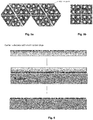
- a display pixel is formed made up of ILED emitters, one from a corner of a plurality of neighbouring monolithic chips. When chips of different wavelengths are tiled in neighbouring positions, a white pixel consisting of 4 emitter elements can then be formed, e.g. Red, Green, Blue, Green pixel configuration. The second green compensates for the lower efficiency that is currently inherent in green LED material. Not all corners of the ILED array chip must have an emitter pixel. For example, an array of RGB could be formed using square chips with emitters at 3 corners and an n-contact or inactive area at the fourth corner.
- a triangular or hexagonal array chip may be used in the formation of 3 pixel white elements, see Figure 2 , as the efficiency of use of material is maximised. This could lead to Red, Green, Blue pixels.
- Figure 2 shows a plurality of ILED array chips that have been assembled onto a substrate using one or more of the assembly techniques discussed above.
- the minimum size of the display pixels (X min ) (which is related to the display resolution) can be defined by (2 x (Dp + D e ) + Sc) where:
- FIG 4 Further illustration of this is shown in Fig 4 .
- Fig 8 gives an overview of the interconnection scheme at the device level. In order to illuminate the blue pixel, a voltage is applied to the p-contact for the Red, Green and Blue sub-pixel. The n-contact for the blue sub-pixel is then grounded which will result in only the blue device illuminating.
- the substrate may be permanent in exemplary methods and apparatus, in particular if the substrate is transparent (e.g. a glass substrate) to the wavelengths emitted by the ILED array chips.
- the substrate may then form an outer surface of the display.
- a display assembly process disclosed combines high resolution ILED array chip array design assembled by micro-assembly methods making them compatible with TFT integration and manufacture.
- the process flows for the first and bullets above are largely the same as the method described above. The main differences are the components (TFT vs CMOS) and final form factor (carrier on or carrier off).
- the resulting array chips comprising a plurality of ILED array chips positioned such that pixels are formed from emitters of adjacent chips, are then assembled on a component of the final display. This is then interconnected with the TFT planar backplane containing TFT control circuitry.
- TFTs using amphorous Silicon (a-Si TFTs), Metal Oxide (MO-TFT's) or low temperature polysilicon (LTPS-TFT's) provide current to the ILEDs, thereby controlling their respective brightness.
- the methods and apparatus disclosed comprise a display assembly process which deploys micro-assembly process which can fit into a cell production line of a LCD/TFT manufacturing line., i.e. replacing the polimide/gasket/liquid crystal injection/glass sandwich/polarizer with corresponding micro-assembly processing steps.
- Module production for IC placement, anisotropic conductive film (ACF) lamination and ribbon cables will be agnostic to OLED or ILED technology.
- the technology is considered not disruptive enough for a TFT line to manufacture.
- An advantage is that unlike LCD/TFT backplanes the micro ILED/TFT design does not suffer fill factor losses due to the need for backlighting.
- the final assembly metal bezel assembly and packaing removes the requirements for backlighting.
- the ILED array chips are designed specifically that multiple colour chips can be assembled in close proximity to essentially produce high density white display pixels directly on the driver backplane.
- the image engine containing the ILED array chips in a display array and a TFT backplane can then be integrated with a controller IC and connected to a PCB motherboard by ACF/FPC cabling.
- the high resolution ILED array chips are mounted directly onto a suitable transparent substrate face up, i.e. with an emitting surface of the ILED array chips facing the transparent substrate.
- the transparent substrate can be temporary or permanently fixed to the ILED array chips.
- the ILED array chips are then connected to a driver backplane and IC controllers using a suitable wireless interconnect bonding method. Wireless direct bonding methods eliminate the need for wirebonds, solder bumping/flipchip techniques thus simplifying interconnections.
- convalent bonds room temperature bonds between silicon oxide or nitride surfaces of each chip are formed.
- the direct bond is characterized by a very high bond energy between the chip surfaces, which includes the metal patterns that form effective electrical connections between the chips. With this technique the low resistance of these electrical connections enables better power efficiency and reduces the overall power consumption of the module.
- control electronics are not transparent.
- active backplanes used in backlit LCD displays
- significant effort is made to minimize the size of the control circuits. This allows the maximum amount of light to travel through pixels without it being blocked by the circuits and wasted.
- a passive matrix drive scheme In a passive matrix drive scheme the anode and cathode control lines are arranged perpendicular to each other.
- the emitter in this case the ILED array chips
- the driver circuitry is located away from the light emitting and transmitting region.
- a benefit of such an arrangement is a simplification of the driver circuitry and an increase in the transparency for the display.
- this approach is limited in the size of the array due to the current that must be driven across multiple pixels and the associated losses.
- small ILED array chips for the image engine greatly reduces the issues associated with the yield losses of large monolithic array chips.
- the monolithic ILED chip When an emitter fails, the monolithic ILED chip must be discarded.
- the discarding of the chip results in a small loss of material.
- a failed emitter results in the discarding of a chip with a large amount of working material and hence results in significant yield losses. It also allows for binning of the ILED array chips based on light output performance and hence provides for more uniform and less complex controller circuitry.
- the integration of the light source directly onto a driver backplane has a number of competitive advantages for higher density interconnect, minimal volume packaging with better performance and reliability
- the methods and apparatus disclosed may also incorporate a passive matrix.
- the benefits of this include the possibility of transparent display that would allow light to travel through it with minimal disruption. Such a concept could be applied to augmented reality systems or display contact lens.
- the ILED emitters may be micro ILED emitters as shown in Figure 9 , which shows a micro ILED structure 900 similar to that proposed in WO 2004/097947 ( US 7,518,149 ) with a high extraction efficiency and outputting quasi-collimated light because of its shape.
- a micro ILED 900 is shown in Figure 3 , wherein a substrate 902 has a semiconductor epitaxial layer 904 located on it. The epitaxial layer 904 is shaped into a mesa 906. An active (or light emitting) layer 908 is enclosed in the mesa structure 906.
- the mesa 906 has a truncated top, on a side opposed to a light transmitting or emitting face 910.
- the mesa 906 also has a near-parabolic shape to form a reflective enclosure for light generated or detected within the device.
- the arrows 912 show how light emitted from the active layer 908 is reflected off the walls of the mesa 906 toward the light exiting surface 910 at an angle sufficient for it to escape the LED device 900 (i.e. within the angle of total internal reflection).
Landscapes
- Engineering & Computer Science (AREA)
- Microelectronics & Electronic Packaging (AREA)
- Power Engineering (AREA)
- Physics & Mathematics (AREA)
- General Physics & Mathematics (AREA)
- Computer Hardware Design (AREA)
- Condensed Matter Physics & Semiconductors (AREA)
- Theoretical Computer Science (AREA)
- Devices For Indicating Variable Information By Combining Individual Elements (AREA)
- Led Device Packages (AREA)
- Electroluminescent Light Sources (AREA)
- Control Of Indicators Other Than Cathode Ray Tubes (AREA)
- Control Of El Displays (AREA)
- Manufacturing & Machinery (AREA)
Priority Applications (1)
| Application Number | Priority Date | Filing Date | Title |
|---|---|---|---|
| EP20215394.6A EP3826055A1 (en) | 2014-07-31 | 2015-07-31 | A colour iled display on silicon |
Applications Claiming Priority (2)
| Application Number | Priority Date | Filing Date | Title |
|---|---|---|---|
| GBGB1413578.4A GB201413578D0 (en) | 2014-07-31 | 2014-07-31 | A colour iled display on silicon |
| PCT/EP2015/067749 WO2016016460A1 (en) | 2014-07-31 | 2015-07-31 | A colour iled display on silicon |
Related Child Applications (2)
| Application Number | Title | Priority Date | Filing Date |
|---|---|---|---|
| EP20215394.6A Division-Into EP3826055A1 (en) | 2014-07-31 | 2015-07-31 | A colour iled display on silicon |
| EP20215394.6A Division EP3826055A1 (en) | 2014-07-31 | 2015-07-31 | A colour iled display on silicon |
Publications (2)
| Publication Number | Publication Date |
|---|---|
| EP3175482A1 EP3175482A1 (en) | 2017-06-07 |
| EP3175482B1 true EP3175482B1 (en) | 2021-05-19 |
Family
ID=51587531
Family Applications (2)
| Application Number | Title | Priority Date | Filing Date |
|---|---|---|---|
| EP15744594.1A Active EP3175482B1 (en) | 2014-07-31 | 2015-07-31 | A colour iled display on silicon |
| EP20215394.6A Pending EP3826055A1 (en) | 2014-07-31 | 2015-07-31 | A colour iled display on silicon |
Family Applications After (1)
| Application Number | Title | Priority Date | Filing Date |
|---|---|---|---|
| EP20215394.6A Pending EP3826055A1 (en) | 2014-07-31 | 2015-07-31 | A colour iled display on silicon |
Country Status (7)
Families Citing this family (83)
| Publication number | Priority date | Publication date | Assignee | Title |
|---|---|---|---|---|
| GB201413578D0 (en) * | 2014-07-31 | 2014-09-17 | Infiniled Ltd | A colour iled display on silicon |
| GB201413604D0 (en) * | 2014-07-31 | 2014-09-17 | Infiniled Ltd | A colour inorganic LED display for display devices with a high number of pixel |
| GB201418810D0 (en) | 2014-10-22 | 2014-12-03 | Infiniled Ltd | Display |
| GB201418772D0 (en) * | 2014-10-22 | 2014-12-03 | Infiniled Ltd | Display |
| GB2586423B (en) * | 2014-10-22 | 2021-09-01 | Facebook Tech Llc | Display |
| US10079264B2 (en) * | 2015-12-21 | 2018-09-18 | Hong Kong Beida Jade Bird Display Limited | Semiconductor devices with integrated thin-film transistor circuitry |
| DE102016108776A1 (de) | 2016-05-12 | 2017-11-16 | Osram Opto Semiconductors Gmbh | Optische Anordnung und Anzeigegerät |
| DE102016113168A1 (de) * | 2016-07-18 | 2018-01-18 | Osram Opto Semiconductors Gmbh | Modul für eine videowand |
| US10606121B2 (en) | 2016-09-12 | 2020-03-31 | Seoul Semiconductor Co., Ltd. | Display apparatus |
| KR20190085516A (ko) * | 2016-12-09 | 2019-07-18 | 어플라이드 머티어리얼스, 인코포레이티드 | 시준된 led 라이트-필드 디스플레이 |
| US10438859B2 (en) | 2016-12-19 | 2019-10-08 | X-Celeprint Limited | Transfer printed device repair |
| CN106898601A (zh) * | 2017-02-15 | 2017-06-27 | 佛山市国星光电股份有限公司 | 三角形组合的led线路板、三角形led器件及显示屏 |
| US10396137B2 (en) * | 2017-03-10 | 2019-08-27 | X-Celeprint Limited | Testing transfer-print micro-devices on wafer |
| US10770440B2 (en) * | 2017-03-15 | 2020-09-08 | Globalfoundries Inc. | Micro-LED display assembly |
| WO2018169968A1 (en) | 2017-03-16 | 2018-09-20 | Invensas Corporation | Direct-bonded led arrays and applications |
| CN106816502B (zh) * | 2017-04-12 | 2019-04-02 | 京东方科技集团股份有限公司 | 一种led芯片、led发光基板、显示装置及彩色显示控制方法 |
| US10490599B2 (en) | 2017-07-13 | 2019-11-26 | Applied Materials, Inc. | Collimated, directional micro-LED light field display |
| US10712579B1 (en) * | 2017-09-20 | 2020-07-14 | Facebook Technologies, Llc | Vortex linearization of micro-LED polarization |
| TWI781241B (zh) * | 2017-11-08 | 2022-10-21 | 美商康寧公司 | 用於組裝顯示區域的裝置及方法 |
| US10836200B2 (en) | 2017-11-13 | 2020-11-17 | X Display Company Technology Limited | Rigid micro-modules with ILED and light conductor |
| US12100696B2 (en) | 2017-11-27 | 2024-09-24 | Seoul Viosys Co., Ltd. | Light emitting diode for display and display apparatus having the same |
| US11282981B2 (en) | 2017-11-27 | 2022-03-22 | Seoul Viosys Co., Ltd. | Passivation covered light emitting unit stack |
| US10892296B2 (en) | 2017-11-27 | 2021-01-12 | Seoul Viosys Co., Ltd. | Light emitting device having commonly connected LED sub-units |
| US11527519B2 (en) | 2017-11-27 | 2022-12-13 | Seoul Viosys Co., Ltd. | LED unit for display and display apparatus having the same |
| US10892297B2 (en) | 2017-11-27 | 2021-01-12 | Seoul Viosys Co., Ltd. | Light emitting diode (LED) stack for a display |
| US10748881B2 (en) | 2017-12-05 | 2020-08-18 | Seoul Viosys Co., Ltd. | Light emitting device with LED stack for display and display apparatus having the same |
| US10886327B2 (en) | 2017-12-14 | 2021-01-05 | Seoul Viosys Co., Ltd. | Light emitting stacked structure and display device having the same |
| US11552057B2 (en) | 2017-12-20 | 2023-01-10 | Seoul Viosys Co., Ltd. | LED unit for display and display apparatus having the same |
| US11522006B2 (en) | 2017-12-21 | 2022-12-06 | Seoul Viosys Co., Ltd. | Light emitting stacked structure and display device having the same |
| US11552061B2 (en) | 2017-12-22 | 2023-01-10 | Seoul Viosys Co., Ltd. | Light emitting device with LED stack for display and display apparatus having the same |
| US11114499B2 (en) * | 2018-01-02 | 2021-09-07 | Seoul Viosys Co., Ltd. | Display device having light emitting stacked structure |
| US10784240B2 (en) | 2018-01-03 | 2020-09-22 | Seoul Viosys Co., Ltd. | Light emitting device with LED stack for display and display apparatus having the same |
| US11169326B2 (en) | 2018-02-26 | 2021-11-09 | Invensas Bonding Technologies, Inc. | Integrated optical waveguides, direct-bonded waveguide interface joints, optical routing and interconnects |
| JP7195653B2 (ja) | 2018-03-01 | 2022-12-26 | ヒーズ アイピー ホールディングス エルエルシー | 視野像の複数の深さを可能にするニアアイディスプレイ表示方法 |
| US11256004B2 (en) | 2018-03-20 | 2022-02-22 | Invensas Bonding Technologies, Inc. | Direct-bonded lamination for improved image clarity in optical devices |
| US11100844B2 (en) * | 2018-04-25 | 2021-08-24 | Raxium, Inc. | Architecture for light emitting elements in a light field display |
| CN112166465B (zh) | 2018-05-31 | 2022-07-12 | 株式会社日本显示器 | 显示装置以及阵列基板 |
| JP6985983B2 (ja) | 2018-05-31 | 2021-12-22 | 株式会社ジャパンディスプレイ | 表示装置 |
| WO2019230229A1 (ja) | 2018-05-31 | 2019-12-05 | 株式会社ジャパンディスプレイ | 表示装置及びアレイ基板 |
| WO2019230250A1 (ja) | 2018-05-31 | 2019-12-05 | 株式会社ジャパンディスプレイ | 表示装置及びアレイ基板 |
| DE112019002234B4 (de) | 2018-05-31 | 2024-09-12 | Japan Display Inc. | Anzeigevorrichtung |
| JP7132779B2 (ja) | 2018-07-18 | 2022-09-07 | 株式会社ジャパンディスプレイ | 表示装置及びアレイ基板 |
| JP7044882B2 (ja) | 2018-07-27 | 2022-03-30 | 株式会社ジャパンディスプレイ | 検出装置付き表示機器 |
| RU201978U1 (ru) * | 2018-08-03 | 2021-01-25 | Акционерное общество "Завод полупроводниковых приборов" | Корпус микросборки |
| DE102018129209B4 (de) * | 2018-11-20 | 2022-04-14 | OSRAM Opto Semiconductors Gesellschaft mit beschränkter Haftung | Multi-pixel-anzeigevorrichtung |
| JP7264669B2 (ja) | 2019-03-01 | 2023-04-25 | 株式会社ジャパンディスプレイ | 表示装置 |
| JP7360246B2 (ja) | 2019-03-14 | 2023-10-12 | 株式会社ジャパンディスプレイ | 表示装置 |
| JP7281940B2 (ja) | 2019-03-28 | 2023-05-26 | 株式会社ジャパンディスプレイ | 検出装置付き表示機器 |
| JP2020166191A (ja) | 2019-03-29 | 2020-10-08 | 株式会社ジャパンディスプレイ | 表示装置 |
| JP7264694B2 (ja) | 2019-03-29 | 2023-04-25 | 株式会社ジャパンディスプレイ | 表示装置 |
| JP7313925B2 (ja) * | 2019-06-25 | 2023-07-25 | 株式会社ジャパンディスプレイ | 表示装置 |
| JP2021026187A (ja) | 2019-08-08 | 2021-02-22 | 株式会社ジャパンディスプレイ | 表示装置 |
| JP7360272B2 (ja) | 2019-08-19 | 2023-10-12 | 株式会社ジャパンディスプレイ | 表示装置 |
| JP2021043373A (ja) | 2019-09-12 | 2021-03-18 | 株式会社ジャパンディスプレイ | 表示装置 |
| JP7300949B2 (ja) | 2019-09-24 | 2023-06-30 | 株式会社ジャパンディスプレイ | 表示装置の補修方法 |
| JP2021051150A (ja) | 2019-09-24 | 2021-04-01 | 株式会社ジャパンディスプレイ | 表示装置の補修方法及び表示装置 |
| JP2021056380A (ja) | 2019-09-30 | 2021-04-08 | 株式会社ジャパンディスプレイ | 表示装置 |
| JP2021056454A (ja) | 2019-10-01 | 2021-04-08 | 株式会社ジャパンディスプレイ | 表示装置 |
| JP7326137B2 (ja) | 2019-12-03 | 2023-08-15 | 株式会社ジャパンディスプレイ | 表示装置 |
| FR3104815B1 (fr) * | 2019-12-17 | 2023-08-25 | Thales Sa | Dispositif d'affichage couleur comportant une mosaique de paves de micro-diodes electroluminescentes |
| US11762200B2 (en) * | 2019-12-17 | 2023-09-19 | Adeia Semiconductor Bonding Technologies Inc. | Bonded optical devices |
| US11355480B1 (en) * | 2020-01-27 | 2022-06-07 | Facebook Technologies, Llc | Micropixellation for alignment-free assembly |
| CN113711296B (zh) | 2020-01-28 | 2025-09-05 | Oled沃克斯有限责任公司 | 具有低压硅背板的堆叠式oled微显示器 |
| US11756947B2 (en) * | 2020-02-06 | 2023-09-12 | Lumileds Llc | Light-emitting diode lighting system with wirebonded hybridized device |
| JP2021153114A (ja) | 2020-03-24 | 2021-09-30 | 株式会社ジャパンディスプレイ | 配線基板及び表示装置 |
| KR102722770B1 (ko) * | 2020-04-13 | 2024-10-29 | 애플 인크. | 디스플레이 뒤의 방출기 |
| KR20230005182A (ko) | 2020-05-01 | 2023-01-09 | 소니 세미컨덕터 솔루션즈 가부시키가이샤 | 표시 장치 및 표면 실장 부품 |
| JP2022025375A (ja) | 2020-07-29 | 2022-02-10 | 株式会社ジャパンディスプレイ | 表示装置 |
| KR102249675B1 (ko) * | 2020-08-25 | 2021-05-10 | 포스텍네트웍스(주) | 영상 저장 fpga를 활용하며 발광 소자 단위로 보정가능한 led 전광판 제어시스템 |
| JP2022041743A (ja) | 2020-09-01 | 2022-03-11 | 株式会社ジャパンディスプレイ | 発光装置及び発光装置の駆動方法 |
| EP4174965A4 (en) * | 2020-09-29 | 2023-09-06 | BOE Technology Group Co., Ltd. | LIGHT-EMITTING DIODE CHIP, DISPLAY SUBSTRATE AND RELATED MANUFACTURING METHOD |
| CN114361148A (zh) * | 2020-09-30 | 2022-04-15 | Tcl科技集团股份有限公司 | 像素结构、灯板、显示装置及像素结构的驱动方法 |
| DE102020130211A1 (de) * | 2020-11-16 | 2022-05-19 | OSRAM Opto Semiconductors Gesellschaft mit beschränkter Haftung | Optoelektronisches Halbleiterbauteil und Verfahren zur Herstellung zumindest eines optoelektronischen Halbleiterbauteils |
| DE102021101657B4 (de) | 2021-01-26 | 2024-12-12 | Infineon Technologies Ag | Verfahren zur Herstellung eines hybriden Bauelements |
| CN113205760B (zh) * | 2021-04-29 | 2023-12-01 | 无锡唐古半导体有限公司 | 硅基微显示器及其驱动电路 |
| US20230017865A1 (en) * | 2021-07-15 | 2023-01-19 | GM Global Technology Operations LLC | Full color microled display controlled by number of red green and blue leds |
| US12336357B2 (en) | 2021-11-24 | 2025-06-17 | Meta Platforms Technologies, Llc | Alignment-free micro-display architecture |
| TWI778883B (zh) * | 2021-12-03 | 2022-09-21 | 友達光電股份有限公司 | 元件陣列基板 |
| CN115172539A (zh) * | 2022-06-23 | 2022-10-11 | 深圳市兆驰光元科技有限公司 | Cob显示面板的制备方法及修复方法 |
| CN115171543B (zh) * | 2022-06-27 | 2023-10-31 | 湖北长江新型显示产业创新中心有限公司 | 显示面板及拼接显示装置 |
| WO2024072873A2 (en) * | 2022-09-29 | 2024-04-04 | Glo Technologies Llc | Light emitting device including led die having portions located in adjacent pixels and method of making same |
| WO2024211607A1 (en) * | 2023-04-05 | 2024-10-10 | Tectus Corporation | Ultra-dense micro-led array with partially overlapping microlenses |
| KR102831649B1 (ko) * | 2023-08-28 | 2025-07-07 | 한국로봇융합연구원 | 수중 보행 로봇용 자석발 장치 |
Family Cites Families (31)
| Publication number | Priority date | Publication date | Assignee | Title |
|---|---|---|---|---|
| US7091986B2 (en) | 1997-09-13 | 2006-08-15 | Gia Chuong Phan | Dynamic pixel resolution, brightness and contrast for displays using spatial elements |
| JP3906653B2 (ja) | 2000-07-18 | 2007-04-18 | ソニー株式会社 | 画像表示装置及びその製造方法 |
| JP2003084690A (ja) | 2001-09-12 | 2003-03-19 | Matsushita Electric Ind Co Ltd | Led表示装置 |
| JP4430010B2 (ja) | 2003-01-24 | 2010-03-10 | 株式会社半導体エネルギー研究所 | 発光装置 |
| US6962835B2 (en) | 2003-02-07 | 2005-11-08 | Ziptronix, Inc. | Method for room temperature metal direct bonding |
| WO2004097947A2 (en) | 2003-05-02 | 2004-11-11 | University College Cork-National University Of Ireland, Cork | Light emitting diodes and the manufacture thereof |
| US7408566B2 (en) * | 2003-10-22 | 2008-08-05 | Oki Data Corporation | Semiconductor device, LED print head and image-forming apparatus using same, and method of manufacturing semiconductor device |
| CN2741133Y (zh) * | 2004-09-07 | 2005-11-16 | 张艳君 | 可共享像素的led点阵显示模块 |
| JP2007027157A (ja) | 2005-07-12 | 2007-02-01 | Akita Denshi Systems:Kk | 発光ダイオード装置及びその製造方法並びに照明装置 |
| JP2007180163A (ja) | 2005-12-27 | 2007-07-12 | Samsung Electronics Co Ltd | 発光デバイスモジュール |
| GB2437110B (en) | 2006-04-12 | 2009-01-28 | Cambridge Display Tech Ltd | Optoelectronic display and method of manufacturing the same |
| JP2008218733A (ja) | 2007-03-05 | 2008-09-18 | Mikku:Kk | カラー表示用ledパネル |
| KR20110039313A (ko) * | 2008-07-07 | 2011-04-15 | 글로 에이비 | 나노구조 led |
| JP2010024557A (ja) | 2008-07-16 | 2010-02-04 | Mitsubishi Rayon Co Ltd | 仮撚加工糸及びその製造方法並びにその織編物 |
| EP2218571A1 (en) * | 2009-01-30 | 2010-08-18 | Nederlandse Organisatie voor toegepast -natuurwetenschappelijk onderzoek TNO | Illumination system for use in a stereolithography apparatus |
| JP4951018B2 (ja) * | 2009-03-30 | 2012-06-13 | 株式会社東芝 | 半導体装置の製造方法 |
| TWI592996B (zh) | 2009-05-12 | 2017-07-21 | 美國伊利諾大學理事會 | 用於可變形及半透明顯示器之超薄微刻度無機發光二極體之印刷總成 |
| DE102009033915B4 (de) * | 2009-07-20 | 2022-05-25 | OSRAM Opto Semiconductors Gesellschaft mit beschränkter Haftung | Verfahren zur Herstellung eines Leuchtmittels und Leuchtmittel |
| US8557616B2 (en) | 2009-12-09 | 2013-10-15 | Nano And Advanced Materials Institute Limited | Method for manufacturing a monolithic LED micro-display on an active matrix panel using flip-chip technology and display apparatus having the monolithic LED micro-display |
| US20130278631A1 (en) * | 2010-02-28 | 2013-10-24 | Osterhout Group, Inc. | 3d positioning of augmented reality information |
| US8835903B2 (en) | 2010-07-29 | 2014-09-16 | National Tsing Hua University | Light-emitting diode display and method of producing the same |
| DE102011016308A1 (de) * | 2011-04-07 | 2012-10-11 | Osram Opto Semiconductors Gmbh | Anzeigevorrichtung |
| JP5966412B2 (ja) | 2011-04-08 | 2016-08-10 | ソニー株式会社 | 画素チップ、表示パネル、照明パネル、表示装置および照明装置 |
| CN102903804B (zh) * | 2011-07-25 | 2015-12-16 | 财团法人工业技术研究院 | 发光元件的转移方法以及发光元件阵列 |
| US8646505B2 (en) * | 2011-11-18 | 2014-02-11 | LuxVue Technology Corporation | Micro device transfer head |
| US9368546B2 (en) * | 2012-02-15 | 2016-06-14 | Microsoft Technology Licensing, Llc | Imaging structure with embedded light sources |
| US20140056003A1 (en) * | 2012-08-20 | 2014-02-27 | John Frattalone | Modular video and lighting displays |
| GB201215632D0 (en) | 2012-09-03 | 2012-10-17 | Infiniled Ltd | Optical device |
| US9029880B2 (en) * | 2012-12-10 | 2015-05-12 | LuxVue Technology Corporation | Active matrix display panel with ground tie lines |
| US9153171B2 (en) | 2012-12-17 | 2015-10-06 | LuxVue Technology Corporation | Smart pixel lighting and display microcontroller |
| GB201413578D0 (en) * | 2014-07-31 | 2014-09-17 | Infiniled Ltd | A colour iled display on silicon |
-
2014
- 2014-07-31 GB GBGB1413578.4A patent/GB201413578D0/en not_active Ceased
-
2015
- 2015-07-31 EP EP15744594.1A patent/EP3175482B1/en active Active
- 2015-07-31 JP JP2017505214A patent/JP6741649B2/ja not_active Expired - Fee Related
- 2015-07-31 KR KR1020177003260A patent/KR102473326B1/ko active Active
- 2015-07-31 EP EP20215394.6A patent/EP3826055A1/en active Pending
- 2015-07-31 WO PCT/EP2015/067749 patent/WO2016016460A1/en active Application Filing
- 2015-07-31 CN CN201580052942.7A patent/CN107078132B/zh active Active
- 2015-07-31 KR KR1020227041481A patent/KR20220164076A/ko not_active Abandoned
- 2015-07-31 KR KR1020227041469A patent/KR20220164074A/ko not_active Abandoned
- 2015-07-31 CN CN202111314127.7A patent/CN113937092A/zh active Pending
- 2015-07-31 CN CN202111315743.4A patent/CN113937093A/zh active Pending
- 2015-07-31 KR KR1020227041476A patent/KR20220164075A/ko not_active Abandoned
- 2015-07-31 US US15/329,552 patent/US10515580B2/en active Active
-
2019
- 2019-11-05 US US16/675,004 patent/US10984705B2/en active Active
-
2020
- 2020-07-27 JP JP2020126764A patent/JP7004777B2/ja active Active
-
2021
- 2021-03-15 US US17/201,381 patent/US11244605B2/en active Active
- 2021-12-29 US US17/564,938 patent/US11468830B2/en active Active
-
2022
- 2022-01-04 JP JP2022000267A patent/JP7248828B2/ja active Active
-
2023
- 2023-03-16 JP JP2023041504A patent/JP7473702B2/ja active Active
Non-Patent Citations (1)
| Title |
|---|
| None * |
Also Published As
| Publication number | Publication date |
|---|---|
| CN113937092A (zh) | 2022-01-14 |
| KR102473326B1 (ko) | 2022-12-05 |
| JP7004777B2 (ja) | 2022-01-21 |
| WO2016016460A1 (en) | 2016-02-04 |
| US10984705B2 (en) | 2021-04-20 |
| US20200126477A1 (en) | 2020-04-23 |
| US20210217356A1 (en) | 2021-07-15 |
| US20170213502A1 (en) | 2017-07-27 |
| KR20220164075A (ko) | 2022-12-12 |
| JP2017529557A (ja) | 2017-10-05 |
| CN113937093A (zh) | 2022-01-14 |
| CN107078132A (zh) | 2017-08-18 |
| JP6741649B2 (ja) | 2020-08-19 |
| JP7248828B2 (ja) | 2023-03-29 |
| JP2023088953A (ja) | 2023-06-27 |
| US11468830B2 (en) | 2022-10-11 |
| KR20220164076A (ko) | 2022-12-12 |
| US10515580B2 (en) | 2019-12-24 |
| US11244605B2 (en) | 2022-02-08 |
| KR20220164074A (ko) | 2022-12-12 |
| CN107078132B (zh) | 2021-11-05 |
| JP2021005087A (ja) | 2021-01-14 |
| EP3826055A1 (en) | 2021-05-26 |
| US20220148495A1 (en) | 2022-05-12 |
| KR20170037975A (ko) | 2017-04-05 |
| JP2022058485A (ja) | 2022-04-12 |
| JP7473702B2 (ja) | 2024-04-23 |
| GB201413578D0 (en) | 2014-09-17 |
| EP3175482A1 (en) | 2017-06-07 |
Similar Documents
| Publication | Publication Date | Title |
|---|---|---|
| US11244605B2 (en) | Colour ILED display on silicon | |
| CN111048656B (zh) | 显示装置及该显示装置的制造方法 | |
| US9977152B2 (en) | Display panels with integrated micro lens array | |
| KR100926963B1 (ko) | 화상표시장치 및 그 제조방법 | |
| US20160179453A1 (en) | Display panel using direct emission pixel arrays | |
| US20180287008A1 (en) | Method for Producing an Optoelectronic Semiconductor Component and Optoelectronic Semiconductor Component | |
| CN113972196A (zh) | 显示器、用于其的led芯片、像素、控制法、计算机程序 | |
| US11069663B2 (en) | Method of producing an optoelectronic semiconductor component, and optoelectronic semiconductor component | |
| TW201822338A (zh) | 顯示器的製作方法 | |
| US10989376B2 (en) | Assembling of strip of micro light emitting diodes onto backplane | |
| WO2025111121A1 (en) | Light-emitting diode with spectrally selective optical element |
Legal Events
| Date | Code | Title | Description |
|---|---|---|---|
| STAA | Information on the status of an ep patent application or granted ep patent |
Free format text: STATUS: THE INTERNATIONAL PUBLICATION HAS BEEN MADE |
|
| 17P | Request for examination filed |
Effective date: 20170220 |
|
| AK | Designated contracting states |
Kind code of ref document: A1 Designated state(s): AL AT BE BG CH CY CZ DE DK EE ES FI FR GB GR HR HU IE IS IT LI LT LU LV MC MK MT NL NO PL PT RO RS SE SI SK SM TR |
|
| AX | Request for extension of the european patent |
Extension state: BA ME |
|
| PUAI | Public reference made under article 153(3) epc to a published international application that has entered the european phase |
Free format text: ORIGINAL CODE: 0009012 |
|
| STAA | Information on the status of an ep patent application or granted ep patent |
Free format text: STATUS: REQUEST FOR EXAMINATION WAS MADE |
|
| DAV | Request for validation of the european patent (deleted) | ||
| DAX | Request for extension of the european patent (deleted) | ||
| STAA | Information on the status of an ep patent application or granted ep patent |
Free format text: STATUS: EXAMINATION IS IN PROGRESS |
|
| RAP1 | Party data changed (applicant data changed or rights of an application transferred) |
Owner name: FACEBOOK TECHNOLOGIES, LLC |
|
| 17Q | First examination report despatched |
Effective date: 20181212 |
|
| RIC1 | Information provided on ipc code assigned before grant |
Ipc: H01L 25/075 20060101AFI20200831BHEP Ipc: G09F 9/302 20060101ALN20200831BHEP |
|
| RIC1 | Information provided on ipc code assigned before grant |
Ipc: H01L 25/075 20060101AFI20200917BHEP Ipc: G09F 9/302 20060101ALN20200917BHEP |
|
| GRAP | Despatch of communication of intention to grant a patent |
Free format text: ORIGINAL CODE: EPIDOSNIGR1 |
|
| STAA | Information on the status of an ep patent application or granted ep patent |
Free format text: STATUS: GRANT OF PATENT IS INTENDED |
|
| INTG | Intention to grant announced |
Effective date: 20201027 |
|
| GRAJ | Information related to disapproval of communication of intention to grant by the applicant or resumption of examination proceedings by the epo deleted |
Free format text: ORIGINAL CODE: EPIDOSDIGR1 |
|
| STAA | Information on the status of an ep patent application or granted ep patent |
Free format text: STATUS: EXAMINATION IS IN PROGRESS |
|
| GRAP | Despatch of communication of intention to grant a patent |
Free format text: ORIGINAL CODE: EPIDOSNIGR1 |
|
| STAA | Information on the status of an ep patent application or granted ep patent |
Free format text: STATUS: GRANT OF PATENT IS INTENDED |
|
| INTC | Intention to grant announced (deleted) | ||
| RIC1 | Information provided on ipc code assigned before grant |
Ipc: G09F 9/302 20060101ALN20210120BHEP Ipc: H01L 25/075 20060101AFI20210120BHEP |
|
| GRAJ | Information related to disapproval of communication of intention to grant by the applicant or resumption of examination proceedings by the epo deleted |
Free format text: ORIGINAL CODE: EPIDOSDIGR1 |
|
| STAA | Information on the status of an ep patent application or granted ep patent |
Free format text: STATUS: EXAMINATION IS IN PROGRESS |
|
| INTG | Intention to grant announced |
Effective date: 20210209 |
|
| GRAP | Despatch of communication of intention to grant a patent |
Free format text: ORIGINAL CODE: EPIDOSNIGR1 |
|
| STAA | Information on the status of an ep patent application or granted ep patent |
Free format text: STATUS: GRANT OF PATENT IS INTENDED |
|
| GRAS | Grant fee paid |
Free format text: ORIGINAL CODE: EPIDOSNIGR3 |
|
| INTC | Intention to grant announced (deleted) | ||
| RIC1 | Information provided on ipc code assigned before grant |
Ipc: H01L 25/075 20060101AFI20210309BHEP Ipc: G09F 9/302 20060101ALN20210309BHEP |
|
| GRAA | (expected) grant |
Free format text: ORIGINAL CODE: 0009210 |
|
| STAA | Information on the status of an ep patent application or granted ep patent |
Free format text: STATUS: THE PATENT HAS BEEN GRANTED |
|
| INTG | Intention to grant announced |
Effective date: 20210330 |
|
| AK | Designated contracting states |
Kind code of ref document: B1 Designated state(s): AL AT BE BG CH CY CZ DE DK EE ES FI FR GB GR HR HU IE IS IT LI LT LU LV MC MK MT NL NO PL PT RO RS SE SI SK SM TR |
|
| REG | Reference to a national code |
Ref country code: GB Ref legal event code: FG4D |
|
| REG | Reference to a national code |
Ref country code: CH Ref legal event code: EP |
|
| REG | Reference to a national code |
Ref country code: DE Ref legal event code: R096 Ref document number: 602015069436 Country of ref document: DE |
|
| REG | Reference to a national code |
Ref country code: AT Ref legal event code: REF Ref document number: 1394830 Country of ref document: AT Kind code of ref document: T Effective date: 20210615 |
|
| REG | Reference to a national code |
Ref country code: IE Ref legal event code: FG4D |
|
| REG | Reference to a national code |
Ref country code: LT Ref legal event code: MG9D |
|
| REG | Reference to a national code |
Ref country code: AT Ref legal event code: MK05 Ref document number: 1394830 Country of ref document: AT Kind code of ref document: T Effective date: 20210519 |
|
| REG | Reference to a national code |
Ref country code: NL Ref legal event code: MP Effective date: 20210519 |
|
| PG25 | Lapsed in a contracting state [announced via postgrant information from national office to epo] |
Ref country code: FI Free format text: LAPSE BECAUSE OF FAILURE TO SUBMIT A TRANSLATION OF THE DESCRIPTION OR TO PAY THE FEE WITHIN THE PRESCRIBED TIME-LIMIT Effective date: 20210519 Ref country code: LT Free format text: LAPSE BECAUSE OF FAILURE TO SUBMIT A TRANSLATION OF THE DESCRIPTION OR TO PAY THE FEE WITHIN THE PRESCRIBED TIME-LIMIT Effective date: 20210519 Ref country code: BG Free format text: LAPSE BECAUSE OF FAILURE TO SUBMIT A TRANSLATION OF THE DESCRIPTION OR TO PAY THE FEE WITHIN THE PRESCRIBED TIME-LIMIT Effective date: 20210819 Ref country code: AT Free format text: LAPSE BECAUSE OF FAILURE TO SUBMIT A TRANSLATION OF THE DESCRIPTION OR TO PAY THE FEE WITHIN THE PRESCRIBED TIME-LIMIT Effective date: 20210519 Ref country code: HR Free format text: LAPSE BECAUSE OF FAILURE TO SUBMIT A TRANSLATION OF THE DESCRIPTION OR TO PAY THE FEE WITHIN THE PRESCRIBED TIME-LIMIT Effective date: 20210519 |
|
| PG25 | Lapsed in a contracting state [announced via postgrant information from national office to epo] |
Ref country code: PT Free format text: LAPSE BECAUSE OF FAILURE TO SUBMIT A TRANSLATION OF THE DESCRIPTION OR TO PAY THE FEE WITHIN THE PRESCRIBED TIME-LIMIT Effective date: 20210920 Ref country code: NO Free format text: LAPSE BECAUSE OF FAILURE TO SUBMIT A TRANSLATION OF THE DESCRIPTION OR TO PAY THE FEE WITHIN THE PRESCRIBED TIME-LIMIT Effective date: 20210819 Ref country code: PL Free format text: LAPSE BECAUSE OF FAILURE TO SUBMIT A TRANSLATION OF THE DESCRIPTION OR TO PAY THE FEE WITHIN THE PRESCRIBED TIME-LIMIT Effective date: 20210519 Ref country code: SE Free format text: LAPSE BECAUSE OF FAILURE TO SUBMIT A TRANSLATION OF THE DESCRIPTION OR TO PAY THE FEE WITHIN THE PRESCRIBED TIME-LIMIT Effective date: 20210519 Ref country code: RS Free format text: LAPSE BECAUSE OF FAILURE TO SUBMIT A TRANSLATION OF THE DESCRIPTION OR TO PAY THE FEE WITHIN THE PRESCRIBED TIME-LIMIT Effective date: 20210519 Ref country code: GR Free format text: LAPSE BECAUSE OF FAILURE TO SUBMIT A TRANSLATION OF THE DESCRIPTION OR TO PAY THE FEE WITHIN THE PRESCRIBED TIME-LIMIT Effective date: 20210820 Ref country code: LV Free format text: LAPSE BECAUSE OF FAILURE TO SUBMIT A TRANSLATION OF THE DESCRIPTION OR TO PAY THE FEE WITHIN THE PRESCRIBED TIME-LIMIT Effective date: 20210519 Ref country code: IS Free format text: LAPSE BECAUSE OF FAILURE TO SUBMIT A TRANSLATION OF THE DESCRIPTION OR TO PAY THE FEE WITHIN THE PRESCRIBED TIME-LIMIT Effective date: 20210919 |
|
| PG25 | Lapsed in a contracting state [announced via postgrant information from national office to epo] |
Ref country code: NL Free format text: LAPSE BECAUSE OF FAILURE TO SUBMIT A TRANSLATION OF THE DESCRIPTION OR TO PAY THE FEE WITHIN THE PRESCRIBED TIME-LIMIT Effective date: 20210519 |
|
| PG25 | Lapsed in a contracting state [announced via postgrant information from national office to epo] |
Ref country code: ES Free format text: LAPSE BECAUSE OF FAILURE TO SUBMIT A TRANSLATION OF THE DESCRIPTION OR TO PAY THE FEE WITHIN THE PRESCRIBED TIME-LIMIT Effective date: 20210519 Ref country code: RO Free format text: LAPSE BECAUSE OF FAILURE TO SUBMIT A TRANSLATION OF THE DESCRIPTION OR TO PAY THE FEE WITHIN THE PRESCRIBED TIME-LIMIT Effective date: 20210519 Ref country code: EE Free format text: LAPSE BECAUSE OF FAILURE TO SUBMIT A TRANSLATION OF THE DESCRIPTION OR TO PAY THE FEE WITHIN THE PRESCRIBED TIME-LIMIT Effective date: 20210519 Ref country code: DK Free format text: LAPSE BECAUSE OF FAILURE TO SUBMIT A TRANSLATION OF THE DESCRIPTION OR TO PAY THE FEE WITHIN THE PRESCRIBED TIME-LIMIT Effective date: 20210519 Ref country code: CZ Free format text: LAPSE BECAUSE OF FAILURE TO SUBMIT A TRANSLATION OF THE DESCRIPTION OR TO PAY THE FEE WITHIN THE PRESCRIBED TIME-LIMIT Effective date: 20210519 Ref country code: SM Free format text: LAPSE BECAUSE OF FAILURE TO SUBMIT A TRANSLATION OF THE DESCRIPTION OR TO PAY THE FEE WITHIN THE PRESCRIBED TIME-LIMIT Effective date: 20210519 Ref country code: SK Free format text: LAPSE BECAUSE OF FAILURE TO SUBMIT A TRANSLATION OF THE DESCRIPTION OR TO PAY THE FEE WITHIN THE PRESCRIBED TIME-LIMIT Effective date: 20210519 |
|
| REG | Reference to a national code |
Ref country code: DE Ref legal event code: R097 Ref document number: 602015069436 Country of ref document: DE |
|
| REG | Reference to a national code |
Ref country code: CH Ref legal event code: PL |
|
| PLBE | No opposition filed within time limit |
Free format text: ORIGINAL CODE: 0009261 |
|
| STAA | Information on the status of an ep patent application or granted ep patent |
Free format text: STATUS: NO OPPOSITION FILED WITHIN TIME LIMIT |
|
| PG25 | Lapsed in a contracting state [announced via postgrant information from national office to epo] |
Ref country code: MC Free format text: LAPSE BECAUSE OF FAILURE TO SUBMIT A TRANSLATION OF THE DESCRIPTION OR TO PAY THE FEE WITHIN THE PRESCRIBED TIME-LIMIT Effective date: 20210519 |
|
| REG | Reference to a national code |
Ref country code: BE Ref legal event code: MM Effective date: 20210731 |
|
| 26N | No opposition filed |
Effective date: 20220222 |
|
| PG25 | Lapsed in a contracting state [announced via postgrant information from national office to epo] |
Ref country code: LI Free format text: LAPSE BECAUSE OF NON-PAYMENT OF DUE FEES Effective date: 20210731 Ref country code: CH Free format text: LAPSE BECAUSE OF NON-PAYMENT OF DUE FEES Effective date: 20210731 |
|
| PG25 | Lapsed in a contracting state [announced via postgrant information from national office to epo] |
Ref country code: IS Free format text: LAPSE BECAUSE OF FAILURE TO SUBMIT A TRANSLATION OF THE DESCRIPTION OR TO PAY THE FEE WITHIN THE PRESCRIBED TIME-LIMIT Effective date: 20210919 Ref country code: LU Free format text: LAPSE BECAUSE OF NON-PAYMENT OF DUE FEES Effective date: 20210731 Ref country code: AL Free format text: LAPSE BECAUSE OF FAILURE TO SUBMIT A TRANSLATION OF THE DESCRIPTION OR TO PAY THE FEE WITHIN THE PRESCRIBED TIME-LIMIT Effective date: 20210519 |
|
| PG25 | Lapsed in a contracting state [announced via postgrant information from national office to epo] |
Ref country code: IT Free format text: LAPSE BECAUSE OF FAILURE TO SUBMIT A TRANSLATION OF THE DESCRIPTION OR TO PAY THE FEE WITHIN THE PRESCRIBED TIME-LIMIT Effective date: 20210519 Ref country code: IE Free format text: LAPSE BECAUSE OF NON-PAYMENT OF DUE FEES Effective date: 20210731 Ref country code: BE Free format text: LAPSE BECAUSE OF NON-PAYMENT OF DUE FEES Effective date: 20210731 |
|
| PG25 | Lapsed in a contracting state [announced via postgrant information from national office to epo] |
Ref country code: HU Free format text: LAPSE BECAUSE OF FAILURE TO SUBMIT A TRANSLATION OF THE DESCRIPTION OR TO PAY THE FEE WITHIN THE PRESCRIBED TIME-LIMIT; INVALID AB INITIO Effective date: 20150731 |
|
| PG25 | Lapsed in a contracting state [announced via postgrant information from national office to epo] |
Ref country code: CY Free format text: LAPSE BECAUSE OF FAILURE TO SUBMIT A TRANSLATION OF THE DESCRIPTION OR TO PAY THE FEE WITHIN THE PRESCRIBED TIME-LIMIT Effective date: 20210519 |
|
| P01 | Opt-out of the competence of the unified patent court (upc) registered |
Effective date: 20230525 |
|
| REG | Reference to a national code |
Ref country code: DE Ref legal event code: R081 Ref document number: 602015069436 Country of ref document: DE Owner name: META PLATFORMS TECHNOLOGIES, LLC, MENLO PARK, US Free format text: FORMER OWNER: FACEBOOK TECHNOLOGIES, LLC, MENLO PARK, CA, US |
|
| PG25 | Lapsed in a contracting state [announced via postgrant information from national office to epo] |
Ref country code: MK Free format text: LAPSE BECAUSE OF FAILURE TO SUBMIT A TRANSLATION OF THE DESCRIPTION OR TO PAY THE FEE WITHIN THE PRESCRIBED TIME-LIMIT Effective date: 20210519 |
|
| PG25 | Lapsed in a contracting state [announced via postgrant information from national office to epo] |
Ref country code: MT Free format text: LAPSE BECAUSE OF FAILURE TO SUBMIT A TRANSLATION OF THE DESCRIPTION OR TO PAY THE FEE WITHIN THE PRESCRIBED TIME-LIMIT Effective date: 20210519 |
|
| PGFP | Annual fee paid to national office [announced via postgrant information from national office to epo] |
Ref country code: DE Payment date: 20240731 Year of fee payment: 10 |
|
| PGFP | Annual fee paid to national office [announced via postgrant information from national office to epo] |
Ref country code: GB Payment date: 20240802 Year of fee payment: 10 |
|
| PGFP | Annual fee paid to national office [announced via postgrant information from national office to epo] |
Ref country code: FR Payment date: 20240724 Year of fee payment: 10 |
|
| REG | Reference to a national code |
Ref country code: DE Ref legal event code: R079 Ref document number: 602015069436 Country of ref document: DE Free format text: PREVIOUS MAIN CLASS: H01L0025075000 Ipc: H10H0029240000 |