JP7360246B2 - 表示装置 - Google Patents
表示装置 Download PDFInfo
- Publication number
- JP7360246B2 JP7360246B2 JP2019047597A JP2019047597A JP7360246B2 JP 7360246 B2 JP7360246 B2 JP 7360246B2 JP 2019047597 A JP2019047597 A JP 2019047597A JP 2019047597 A JP2019047597 A JP 2019047597A JP 7360246 B2 JP7360246 B2 JP 7360246B2
- Authority
- JP
- Japan
- Prior art keywords
- heating resistor
- electrode
- light emitting
- pixel
- display device
- Prior art date
- Legal status (The legal status is an assumption and is not a legal conclusion. Google has not performed a legal analysis and makes no representation as to the accuracy of the status listed.)
- Active
Links
Images


Classifications
-
- G—PHYSICS
- G09—EDUCATION; CRYPTOGRAPHY; DISPLAY; ADVERTISING; SEALS
- G09G—ARRANGEMENTS OR CIRCUITS FOR CONTROL OF INDICATING DEVICES USING STATIC MEANS TO PRESENT VARIABLE INFORMATION
- G09G3/00—Control arrangements or circuits, of interest only in connection with visual indicators other than cathode-ray tubes
- G09G3/20—Control arrangements or circuits, of interest only in connection with visual indicators other than cathode-ray tubes for presentation of an assembly of a number of characters, e.g. a page, by composing the assembly by combination of individual elements arranged in a matrix no fixed position being assigned to or needed to be assigned to the individual characters or partial characters
- G09G3/22—Control arrangements or circuits, of interest only in connection with visual indicators other than cathode-ray tubes for presentation of an assembly of a number of characters, e.g. a page, by composing the assembly by combination of individual elements arranged in a matrix no fixed position being assigned to or needed to be assigned to the individual characters or partial characters using controlled light sources
- G09G3/30—Control arrangements or circuits, of interest only in connection with visual indicators other than cathode-ray tubes for presentation of an assembly of a number of characters, e.g. a page, by composing the assembly by combination of individual elements arranged in a matrix no fixed position being assigned to or needed to be assigned to the individual characters or partial characters using controlled light sources using electroluminescent panels
- G09G3/32—Control arrangements or circuits, of interest only in connection with visual indicators other than cathode-ray tubes for presentation of an assembly of a number of characters, e.g. a page, by composing the assembly by combination of individual elements arranged in a matrix no fixed position being assigned to or needed to be assigned to the individual characters or partial characters using controlled light sources using electroluminescent panels semiconductive, e.g. using light-emitting diodes [LED]
-
- H—ELECTRICITY
- H10—SEMICONDUCTOR DEVICES; ELECTRIC SOLID-STATE DEVICES NOT OTHERWISE PROVIDED FOR
- H10W—GENERIC PACKAGES, INTERCONNECTIONS, CONNECTORS OR OTHER CONSTRUCTIONAL DETAILS OF DEVICES COVERED BY CLASS H10
- H10W90/00—Package configurations
-
- G—PHYSICS
- G09—EDUCATION; CRYPTOGRAPHY; DISPLAY; ADVERTISING; SEALS
- G09F—DISPLAYING; ADVERTISING; SIGNS; LABELS OR NAME-PLATES; SEALS
- G09F9/00—Indicating arrangements for variable information in which the information is built-up on a support by selection or combination of individual elements
- G09F9/30—Indicating arrangements for variable information in which the information is built-up on a support by selection or combination of individual elements in which the desired character or characters are formed by combining individual elements
-
- H—ELECTRICITY
- H10—SEMICONDUCTOR DEVICES; ELECTRIC SOLID-STATE DEVICES NOT OTHERWISE PROVIDED FOR
- H10H—INORGANIC LIGHT-EMITTING SEMICONDUCTOR DEVICES HAVING POTENTIAL BARRIERS
- H10H29/00—Integrated devices, or assemblies of multiple devices, comprising at least one light-emitting semiconductor element covered by group H10H20/00
- H10H29/10—Integrated devices comprising at least one light-emitting semiconductor component covered by group H10H20/00
- H10H29/14—Integrated devices comprising at least one light-emitting semiconductor component covered by group H10H20/00 comprising multiple light-emitting semiconductor components
- H10H29/142—Two-dimensional arrangements, e.g. asymmetric LED layout
-
- H—ELECTRICITY
- H10—SEMICONDUCTOR DEVICES; ELECTRIC SOLID-STATE DEVICES NOT OTHERWISE PROVIDED FOR
- H10W—GENERIC PACKAGES, INTERCONNECTIONS, CONNECTORS OR OTHER CONSTRUCTIONAL DETAILS OF DEVICES COVERED BY CLASS H10
- H10W40/00—Arrangements for thermal protection or thermal control
-
- G—PHYSICS
- G09—EDUCATION; CRYPTOGRAPHY; DISPLAY; ADVERTISING; SEALS
- G09G—ARRANGEMENTS OR CIRCUITS FOR CONTROL OF INDICATING DEVICES USING STATIC MEANS TO PRESENT VARIABLE INFORMATION
- G09G2300/00—Aspects of the constitution of display devices
- G09G2300/04—Structural and physical details of display devices
- G09G2300/0421—Structural details of the set of electrodes
- G09G2300/0426—Layout of electrodes and connections
-
- G—PHYSICS
- G09—EDUCATION; CRYPTOGRAPHY; DISPLAY; ADVERTISING; SEALS
- G09G—ARRANGEMENTS OR CIRCUITS FOR CONTROL OF INDICATING DEVICES USING STATIC MEANS TO PRESENT VARIABLE INFORMATION
- G09G2300/00—Aspects of the constitution of display devices
- G09G2300/04—Structural and physical details of display devices
- G09G2300/0439—Pixel structures
- G09G2300/0452—Details of colour pixel setup, e.g. pixel composed of a red, a blue and two green components
-
- G—PHYSICS
- G09—EDUCATION; CRYPTOGRAPHY; DISPLAY; ADVERTISING; SEALS
- G09G—ARRANGEMENTS OR CIRCUITS FOR CONTROL OF INDICATING DEVICES USING STATIC MEANS TO PRESENT VARIABLE INFORMATION
- G09G2300/00—Aspects of the constitution of display devices
- G09G2300/08—Active matrix structure, i.e. with use of active elements, inclusive of non-linear two terminal elements, in the pixels together with light emitting or modulating elements
- G09G2300/0809—Several active elements per pixel in active matrix panels
- G09G2300/0819—Several active elements per pixel in active matrix panels used for counteracting undesired variations, e.g. feedback or autozeroing
-
- G—PHYSICS
- G09—EDUCATION; CRYPTOGRAPHY; DISPLAY; ADVERTISING; SEALS
- G09G—ARRANGEMENTS OR CIRCUITS FOR CONTROL OF INDICATING DEVICES USING STATIC MEANS TO PRESENT VARIABLE INFORMATION
- G09G2300/00—Aspects of the constitution of display devices
- G09G2300/08—Active matrix structure, i.e. with use of active elements, inclusive of non-linear two terminal elements, in the pixels together with light emitting or modulating elements
- G09G2300/0809—Several active elements per pixel in active matrix panels
- G09G2300/0842—Several active elements per pixel in active matrix panels forming a memory circuit, e.g. a dynamic memory with one capacitor
- G09G2300/0852—Several active elements per pixel in active matrix panels forming a memory circuit, e.g. a dynamic memory with one capacitor being a dynamic memory with more than one capacitor
-
- G—PHYSICS
- G09—EDUCATION; CRYPTOGRAPHY; DISPLAY; ADVERTISING; SEALS
- G09G—ARRANGEMENTS OR CIRCUITS FOR CONTROL OF INDICATING DEVICES USING STATIC MEANS TO PRESENT VARIABLE INFORMATION
- G09G2320/00—Control of display operating conditions
- G09G2320/04—Maintaining the quality of display appearance
- G09G2320/041—Temperature compensation
Landscapes
- Engineering & Computer Science (AREA)
- Physics & Mathematics (AREA)
- General Physics & Mathematics (AREA)
- Theoretical Computer Science (AREA)
- Computer Hardware Design (AREA)
- Control Of Indicators Other Than Cathode Ray Tubes (AREA)
- Control Of El Displays (AREA)
- Electroluminescent Light Sources (AREA)
- Devices For Indicating Variable Information By Combining Individual Elements (AREA)
Description
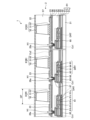
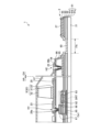
図1は、第1実施形態に係る表示装置を模式的に示す平面図である。図1に示すように、表示装置1は、アレイ基板2と、画素Pixと、駆動回路12と、駆動IC(Integrated Circuit)210と、カソード配線60と、を含む。アレイ基板2は、各画素Pixを駆動するための駆動回路基板であり、バックプレーン又はアクティブマトリックス基板とも呼ばれる。アレイ基板2は、基板21、複数のトランジスタ、複数の容量及び各種配線等を有する。
図12は、第2実施形態に係る画素回路を示す回路図である。なお、以下の説明においては、上述した実施形態で説明したものと同じ構成要素には同一の符号を付して重複する説明は省略する。
図13は、第3実施形態に係る画素回路を示す回路図である。図13に示すように、第3実施形態に係る画素回路PICAは、第1実施形態に比べて、発熱抵抗体28の一端側28e1が、カソード電極22に電気的に接続される構成が異なる。発熱抵抗体28の他端側28e2は、第1実施形態と同様に、発熱制御トランジスタHSTを介してアノード電源線L1に電気的に接続される。
図14は、第4実施形態に係る、温度センサを有する画素を示す平面図である。図15は、温度センサの一例を説明するための説明図である。図14に示すように、表示装置1Aは、画素Pixに温度センサ8及び温度センサ回路81を有する。温度センサ8は、例えばpn接合ダイオードを用いることができる。温度センサ回路81は、温度センサ8を駆動するための回路である。温度センサ回路81は、複数のトランジスタ等の回路素子を備え、温度センサ8への駆動信号の供給を制御する。
2 アレイ基板
3、3R、3G、3B 発光素子
8 温度センサ
12 駆動回路
21 基板
22 カソード電極
23 アノード電極
27 端子部
28 発熱抵抗体
28R 第1発熱抵抗体
28G 第2発熱抵抗体
28B 第3発熱抵抗体
28e1 一端側
28e2 他端側
31 半導体層
32 カソード端子
33 アノード端子
49 副画素
60 カソード配線
210 駆動IC
DRT 駆動トランジスタ
BCT 発光制御トランジスタ
IST 初期化トランジスタ
SST 書込トランジスタ
RST リセットトランジスタ
HST 発熱制御トランジスタ
BG 発光制御走査線
HG 発熱制御走査線
IG 初期化制御走査線
RG リセット制御走査線
SG 書込制御走査線
L1 アノード電源線
L10 カソード電源線
Pix 画素
PICA 画素回路
Claims (11)
- 基板と、
前記基板に設けられた複数の画素と、
複数の前記画素の各々に設けられる発光素子と、
前記基板に設けられ、前記発光素子と電気的に接続される第1電極と、
前記第1電極と電気的に接続されるトランジスタと、
前記基板に設けられ、前記発光素子に駆動信号を供給する画素回路と、
前記画素回路に設けられた発熱抵抗体と、を有し、
前記発熱抵抗体は、前記第1電極よりも高いシート抵抗値を有し、
前記基板に垂直な方向からの平面視で、前記発熱抵抗体はミアンダ状の配線パターンを有し、
前記複数の画素の一は、赤色の赤色を表示する第1副画素と、緑色を表示する第2副画素と、青色を表示する第3副画素とを含み、
前記第1副画素は、前記発熱抵抗体として第1発熱抵抗体を有し、
前記第2副画素は、前記発熱抵抗体として第2発熱抵抗体を有し、
前記第3副画素は、前記発熱抵抗体として第3発熱抵抗体を有し、
前記第1副画素が有する前記第1発熱抵抗体の抵抗値は、前記第2発熱抵抗体の抵抗値及び前記第3発熱抵抗体の抵抗値よりも小さい
表示装置。 - 前記発熱抵抗体の一端側は前記第1電極に電気的に接続される
請求項1に記載の表示装置。 - 前記基板に設けられ、前記発光素子と電気的に接続される第2電極と、
前記第2電極を介して、第2電位を前記発光素子に供給する第2電源線と、を有し、
前記発熱抵抗体の一端側は前記第2電極に電気的に接続される
請求項1に記載の表示装置。 - 前記画素回路は、前記第1電極を介して、前記発光素子に第1電位を供給する第1電源線を有し、
前記発熱抵抗体の他端側は前記第1電源線に電気的に接続される
請求項2又は請求項3に記載の表示装置。 - 前記画素回路は、前記発熱抵抗体に抵抗体駆動信号を供給する抵抗体信号線を有し、
前記発熱抵抗体の他端側は前記抵抗体信号線に電気的に接続される
請求項2又は請求項3に記載の表示装置。 - 前記第1電極の少なくとも一部は、前記基板に垂直な方向からの平面視で、前記発熱抵抗体と重なって設けられる
請求項1から請求項5のいずれか1項に記載の表示装置。 - 複数の前記発光素子の間に設けられ、複数の前記発光素子の少なくとも側面の一部を覆う素子絶縁膜を有し、
前記第2電極は、複数の前記発光素子及び前記素子絶縁膜を覆って、複数の前記発光素子に電気的に接続される
請求項3に記載の表示装置。 - 前記発熱抵抗体は、絶縁膜を介して前記第1電極と異なる層に設けられ、前記絶縁膜に設けられたコンタクトホールを介して前記第1電極と接続される
請求項1から請求項7のいずれか1項に記載の表示装置。 - 前記トランジスタに映像信号を供給する信号線をさらに有し、
前記基板に垂直な方向において、前記信号線、前記発熱抵抗体、前記第1電極の順に積層される
請求項1から請求項8のいずれか1項に記載の表示装置。 - 前記画素に設けられた温度センサと、
前記温度センサからの出力信号を受け取って、前記出力信号の温度依存性に基づいて温度を検出する検出回路と、を有する
請求項1から請求項9のいずれか1項に記載の表示装置。 - 前記発熱抵抗体は、前記トランジスタよりも上層であって、前記第1電極よりも下層に設けられる
請求項1から請求項10のいずれか1項に記載の表示装置。
Priority Applications (4)
| Application Number | Priority Date | Filing Date | Title |
|---|---|---|---|
| JP2019047597A JP7360246B2 (ja) | 2019-03-14 | 2019-03-14 | 表示装置 |
| PCT/JP2019/050422 WO2020183861A1 (ja) | 2019-03-14 | 2019-12-23 | 表示装置 |
| TW109107779A TWI738242B (zh) | 2019-03-14 | 2020-03-10 | 顯示裝置 |
| US17/471,202 US11721276B2 (en) | 2019-03-14 | 2021-09-10 | Display device |
Applications Claiming Priority (1)
| Application Number | Priority Date | Filing Date | Title |
|---|---|---|---|
| JP2019047597A JP7360246B2 (ja) | 2019-03-14 | 2019-03-14 | 表示装置 |
Publications (3)
| Publication Number | Publication Date |
|---|---|
| JP2020148964A JP2020148964A (ja) | 2020-09-17 |
| JP2020148964A5 JP2020148964A5 (ja) | 2022-03-22 |
| JP7360246B2 true JP7360246B2 (ja) | 2023-10-12 |
Family
ID=72427423
Family Applications (1)
| Application Number | Title | Priority Date | Filing Date |
|---|---|---|---|
| JP2019047597A Active JP7360246B2 (ja) | 2019-03-14 | 2019-03-14 | 表示装置 |
Country Status (4)
| Country | Link |
|---|---|
| US (1) | US11721276B2 (ja) |
| JP (1) | JP7360246B2 (ja) |
| TW (1) | TWI738242B (ja) |
| WO (1) | WO2020183861A1 (ja) |
Families Citing this family (8)
| Publication number | Priority date | Publication date | Assignee | Title |
|---|---|---|---|---|
| JP7706170B2 (ja) * | 2020-10-30 | 2025-07-11 | 三国電子有限会社 | タッチ及び指紋センサ付き表示装置 |
| KR102810624B1 (ko) * | 2021-02-23 | 2025-05-22 | 삼성디스플레이 주식회사 | 픽셀 회로, 이를 포함하는 표시 장치 및 이의 구동 방법 |
| CN113870791B (zh) * | 2021-10-11 | 2023-07-25 | 京东方科技集团股份有限公司 | 像素驱动电路及其驱动方法 |
| KR20230095457A (ko) * | 2021-12-22 | 2023-06-29 | 엘지디스플레이 주식회사 | 저전위배선을 포함하는 유기발광다이오드 표시장치 |
| US11961822B2 (en) | 2022-01-17 | 2024-04-16 | Samsung Display Co., Ltd. | Display device, and tiled display device including the display device |
| CN114882816B (zh) * | 2022-06-16 | 2025-01-14 | 厦门天马微电子有限公司 | 显示面板及其检测方法、显示装置 |
| JP2024171113A (ja) * | 2023-05-29 | 2024-12-11 | 株式会社ジャパンディスプレイ | 電子装置の温度調整方法および電子装置 |
| KR20250071980A (ko) * | 2023-11-15 | 2025-05-23 | 엘지디스플레이 주식회사 | 표시 장치 및 그 제조방법 |
Citations (6)
| Publication number | Priority date | Publication date | Assignee | Title |
|---|---|---|---|---|
| JP2002307734A (ja) | 2001-03-29 | 2002-10-23 | Shandong Hualing Electronics Co Ltd | サーマルプリンターヘッド及びその製造方法 |
| JP2005309731A (ja) | 2004-04-21 | 2005-11-04 | Toppan Printing Co Ltd | 基板設計装置、基板設計方法および基板設計プログラム |
| JP2005321684A (ja) | 2004-05-11 | 2005-11-17 | Sony Corp | 映像表示装置および映像表示方法 |
| US20050258446A1 (en) | 2004-05-18 | 2005-11-24 | New Millennium Media International Inc. | LED assembly with vented circuit board |
| JP2007081094A (ja) | 2005-09-14 | 2007-03-29 | Seiko Epson Corp | 発光装置及び電子機器 |
| JP2014082383A (ja) | 2012-10-17 | 2014-05-08 | Kyocera Corp | 発光ユニット、発光制御ユニット、および発光装置 |
Family Cites Families (15)
| Publication number | Priority date | Publication date | Assignee | Title |
|---|---|---|---|---|
| US6879110B2 (en) * | 2000-07-27 | 2005-04-12 | Semiconductor Energy Laboratory Co., Ltd. | Method of driving display device |
| KR100912320B1 (ko) * | 2001-09-07 | 2009-08-14 | 파나소닉 주식회사 | El 표시 장치 |
| US6911624B2 (en) * | 2002-08-23 | 2005-06-28 | Micron Technology, Inc. | Component installation, removal, and replacement apparatus and method |
| JP2012231083A (ja) * | 2011-04-27 | 2012-11-22 | Hitachi Consumer Electronics Co Ltd | バックライト及びそれを用いた液晶表示装置 |
| JP6152801B2 (ja) * | 2014-01-21 | 2017-06-28 | 豊田合成株式会社 | 発光装置及びその製造方法 |
| JP2015215780A (ja) * | 2014-05-12 | 2015-12-03 | 株式会社ジャパンディスプレイ | 表示装置 |
| GB201413578D0 (en) | 2014-07-31 | 2014-09-17 | Infiniled Ltd | A colour iled display on silicon |
| US9728125B2 (en) * | 2014-12-22 | 2017-08-08 | Shenzhen China Star Optoelectronics Technology Co., Ltd | AMOLED pixel circuit |
| KR102601579B1 (ko) * | 2015-12-16 | 2023-11-13 | 삼성전자주식회사 | 발광소자 실장용 회로 기판 및 이를 이용한 반도체 발광소자 패키지 |
| CN106652877B (zh) * | 2017-02-09 | 2020-02-14 | 京东方科技集团股份有限公司 | 显示面板和显示装置 |
| JP2019061929A (ja) * | 2017-09-28 | 2019-04-18 | シャープ株式会社 | 照明装置及びそれを備えた表示装置 |
| CN107452345B (zh) * | 2017-09-29 | 2020-01-10 | 京东方科技集团股份有限公司 | 一种显示器件亮度补偿方法、装置及显示装置 |
| CN110136622B (zh) * | 2018-02-02 | 2022-09-23 | 上海和辉光电股份有限公司 | 一种显示面板、显示装置、显示数据的处理方法及装置 |
| CN108649026A (zh) * | 2018-07-06 | 2018-10-12 | 易美芯光(北京)科技有限公司 | 一种可调色温的led结构 |
| CN109360525A (zh) * | 2018-09-13 | 2019-02-19 | 天长市辉盛电子有限公司 | Led显示屏系统的控制方法及led显示屏系统 |
-
2019
- 2019-03-14 JP JP2019047597A patent/JP7360246B2/ja active Active
- 2019-12-23 WO PCT/JP2019/050422 patent/WO2020183861A1/ja not_active Ceased
-
2020
- 2020-03-10 TW TW109107779A patent/TWI738242B/zh active
-
2021
- 2021-09-10 US US17/471,202 patent/US11721276B2/en active Active
Patent Citations (6)
| Publication number | Priority date | Publication date | Assignee | Title |
|---|---|---|---|---|
| JP2002307734A (ja) | 2001-03-29 | 2002-10-23 | Shandong Hualing Electronics Co Ltd | サーマルプリンターヘッド及びその製造方法 |
| JP2005309731A (ja) | 2004-04-21 | 2005-11-04 | Toppan Printing Co Ltd | 基板設計装置、基板設計方法および基板設計プログラム |
| JP2005321684A (ja) | 2004-05-11 | 2005-11-17 | Sony Corp | 映像表示装置および映像表示方法 |
| US20050258446A1 (en) | 2004-05-18 | 2005-11-24 | New Millennium Media International Inc. | LED assembly with vented circuit board |
| JP2007081094A (ja) | 2005-09-14 | 2007-03-29 | Seiko Epson Corp | 発光装置及び電子機器 |
| JP2014082383A (ja) | 2012-10-17 | 2014-05-08 | Kyocera Corp | 発光ユニット、発光制御ユニット、および発光装置 |
Also Published As
| Publication number | Publication date |
|---|---|
| US11721276B2 (en) | 2023-08-08 |
| WO2020183861A1 (ja) | 2020-09-17 |
| JP2020148964A (ja) | 2020-09-17 |
| TWI738242B (zh) | 2021-09-01 |
| TW202040548A (zh) | 2020-11-01 |
| US20210407385A1 (en) | 2021-12-30 |
Similar Documents
| Publication | Publication Date | Title |
|---|---|---|
| JP7360246B2 (ja) | 表示装置 | |
| TWI715052B (zh) | 顯示裝置 | |
| US11410595B2 (en) | Display device and driving method for display device | |
| TWI756731B (zh) | 顯示裝置 | |
| CN111326673B (zh) | 显示装置 | |
| CN108511485A (zh) | 显示装置 | |
| WO2020189047A1 (ja) | 表示装置 | |
| KR20150019129A (ko) | 표시 장치 | |
| US12142714B2 (en) | Display device | |
| KR20200138543A (ko) | 표시 장치 및 표시 장치의 제조 방법 | |
| WO2020084898A1 (ja) | 表示装置 | |
| US11508292B2 (en) | Display device | |
| US20250096216A1 (en) | Display device | |
| JP7264669B2 (ja) | 表示装置 | |
| CN115621398B (zh) | 显示装置 | |
| US12588347B2 (en) | Display device | |
| US20230025876A1 (en) | Display device | |
| US20230387374A1 (en) | Display device | |
| KR102292516B1 (ko) | 표시 장치 |
Legal Events
| Date | Code | Title | Description |
|---|---|---|---|
| A521 | Request for written amendment filed |
Free format text: JAPANESE INTERMEDIATE CODE: A523 Effective date: 20220311 |
|
| A621 | Written request for application examination |
Free format text: JAPANESE INTERMEDIATE CODE: A621 Effective date: 20220311 |
|
| A131 | Notification of reasons for refusal |
Free format text: JAPANESE INTERMEDIATE CODE: A131 Effective date: 20230411 |
|
| A521 | Request for written amendment filed |
Free format text: JAPANESE INTERMEDIATE CODE: A523 Effective date: 20230612 |
|
| TRDD | Decision of grant or rejection written | ||
| A01 | Written decision to grant a patent or to grant a registration (utility model) |
Free format text: JAPANESE INTERMEDIATE CODE: A01 Effective date: 20230905 |
|
| A61 | First payment of annual fees (during grant procedure) |
Free format text: JAPANESE INTERMEDIATE CODE: A61 Effective date: 20230929 |
|
| R150 | Certificate of patent or registration of utility model |
Ref document number: 7360246 Country of ref document: JP Free format text: JAPANESE INTERMEDIATE CODE: R150 |