EP3172694B1 - High-resolution electric field sensor in cover glass - Google Patents
High-resolution electric field sensor in cover glass Download PDFInfo
- Publication number
- EP3172694B1 EP3172694B1 EP15745343.2A EP15745343A EP3172694B1 EP 3172694 B1 EP3172694 B1 EP 3172694B1 EP 15745343 A EP15745343 A EP 15745343A EP 3172694 B1 EP3172694 B1 EP 3172694B1
- Authority
- EP
- European Patent Office
- Prior art keywords
- layer
- glass
- sensor
- receive
- transmit
- Prior art date
- Legal status (The legal status is an assumption and is not a legal conclusion. Google has not performed a legal analysis and makes no representation as to the accuracy of the status listed.)
- Active
Links
Images

Classifications
-
- G—PHYSICS
- G06—COMPUTING OR CALCULATING; COUNTING
- G06V—IMAGE OR VIDEO RECOGNITION OR UNDERSTANDING
- G06V40/00—Recognition of biometric, human-related or animal-related patterns in image or video data
- G06V40/10—Human or animal bodies, e.g. vehicle occupants or pedestrians; Body parts, e.g. hands
- G06V40/12—Fingerprints or palmprints
- G06V40/13—Sensors therefor
- G06V40/1329—Protecting the fingerprint sensor against damage caused by the finger
-
- G—PHYSICS
- G01—MEASURING; TESTING
- G01R—MEASURING ELECTRIC VARIABLES; MEASURING MAGNETIC VARIABLES
- G01R27/00—Arrangements for measuring resistance, reactance, impedance, or electric characteristics derived therefrom
- G01R27/02—Measuring real or complex resistance, reactance, impedance, or other two-pole characteristics derived therefrom, e.g. time constant
- G01R27/26—Measuring inductance or capacitance; Measuring quality factor, e.g. by using the resonance method; Measuring loss factor; Measuring dielectric constants ; Measuring impedance or related variables
- G01R27/2605—Measuring capacitance
-
- G—PHYSICS
- G06—COMPUTING OR CALCULATING; COUNTING
- G06F—ELECTRIC DIGITAL DATA PROCESSING
- G06F3/00—Input arrangements for transferring data to be processed into a form capable of being handled by the computer; Output arrangements for transferring data from processing unit to output unit, e.g. interface arrangements
- G06F3/01—Input arrangements or combined input and output arrangements for interaction between user and computer
- G06F3/017—Gesture based interaction, e.g. based on a set of recognized hand gestures
-
- G—PHYSICS
- G06—COMPUTING OR CALCULATING; COUNTING
- G06V—IMAGE OR VIDEO RECOGNITION OR UNDERSTANDING
- G06V40/00—Recognition of biometric, human-related or animal-related patterns in image or video data
- G06V40/10—Human or animal bodies, e.g. vehicle occupants or pedestrians; Body parts, e.g. hands
- G06V40/12—Fingerprints or palmprints
- G06V40/13—Sensors therefor
- G06V40/1306—Sensors therefor non-optical, e.g. ultrasonic or capacitive sensing
-
- G—PHYSICS
- G02—OPTICS
- G02F—OPTICAL DEVICES OR ARRANGEMENTS FOR THE CONTROL OF LIGHT BY MODIFICATION OF THE OPTICAL PROPERTIES OF THE MEDIA OF THE ELEMENTS INVOLVED THEREIN; NON-LINEAR OPTICS; FREQUENCY-CHANGING OF LIGHT; OPTICAL LOGIC ELEMENTS; OPTICAL ANALOGUE/DIGITAL CONVERTERS
- G02F1/00—Devices or arrangements for the control of the intensity, colour, phase, polarisation or direction of light arriving from an independent light source, e.g. switching, gating or modulating; Non-linear optics
- G02F1/01—Devices or arrangements for the control of the intensity, colour, phase, polarisation or direction of light arriving from an independent light source, e.g. switching, gating or modulating; Non-linear optics for the control of the intensity, phase, polarisation or colour
- G02F1/13—Devices or arrangements for the control of the intensity, colour, phase, polarisation or direction of light arriving from an independent light source, e.g. switching, gating or modulating; Non-linear optics for the control of the intensity, phase, polarisation or colour based on liquid crystals, e.g. single liquid crystal display cells
- G02F1/133—Constructional arrangements; Operation of liquid crystal cells; Circuit arrangements
- G02F1/1333—Constructional arrangements; Manufacturing methods
- G02F1/13338—Input devices, e.g. touch panels
-
- H—ELECTRICITY
- H10—SEMICONDUCTOR DEVICES; ELECTRIC SOLID-STATE DEVICES NOT OTHERWISE PROVIDED FOR
- H10K—ORGANIC ELECTRIC SOLID-STATE DEVICES
- H10K50/00—Organic light-emitting devices
- H10K50/80—Constructional details
- H10K50/84—Passivation; Containers; Encapsulations
-
- H—ELECTRICITY
- H10—SEMICONDUCTOR DEVICES; ELECTRIC SOLID-STATE DEVICES NOT OTHERWISE PROVIDED FOR
- H10K—ORGANIC ELECTRIC SOLID-STATE DEVICES
- H10K59/00—Integrated devices, or assemblies of multiple devices, comprising at least one organic light-emitting element covered by group H10K50/00
- H10K59/40—OLEDs integrated with touch screens
-
- H—ELECTRICITY
- H10—SEMICONDUCTOR DEVICES; ELECTRIC SOLID-STATE DEVICES NOT OTHERWISE PROVIDED FOR
- H10K—ORGANIC ELECTRIC SOLID-STATE DEVICES
- H10K59/00—Integrated devices, or assemblies of multiple devices, comprising at least one organic light-emitting element covered by group H10K50/00
- H10K59/80—Constructional details
- H10K59/87—Passivation; Containers; Encapsulations
Definitions
- Electronic devices utilizing a touchscreen are prevalent in today's technology.
- Electronic devices using a touchscreen can include, for example, a smartphone, a smartwatch, or a tablet computer.
- a touchscreen can include an electronic visual display that a user can control through simple or multi-touch gestures by touching the screen, for example with a finger. The user can use the touchscreen to react to what is displayed and to control how it is displayed (for example by zooming the text size).
- the touchscreen enables the user to interact directly with what is displayed, rather than using a mouse, touchpad, or any other intermediate device (other than a stylus, which is optional for most modern touchscreens).
- Fingerprint sensors can include a device used to capture an image of a fingerprint pattern. These fingerprint patterns can be used to create a representative template, which can be stored and used for matching an individual's fingerprint.
- US 2012134549 A1 discloses a sensor having a plurality of substantially parallel drive lines configured to transmit a signal into a surface of a proximally located object, and also a plurality of substantially parallel pickup lines oriented proximate the drive lines and electrically separated from the pickup lines to form intrinsic electrode pairs that are impedance sensitive at each of the drive and pickup proximal locations
- a high-resolution electric field-sensor fabricated on a cover glass is described.
- the cover glass is placed above a display to protect the display device from scratches, breakage, and other damage.
- the high-resolution elecric-field sensor can resolve the fine features of a fingerprint on the cover glass while still imaging fingers, styli, palms, and human body parts both on the cover glass and above the cover glass.
- the cover glass retains its strength, scratch resistance, and transparency even in the presence of the high-resolution electric-field sensor. The result is that sensing of many different objects can be done above the display.
- a fingerprint sensor that includes a thin protective cover layer on a sensor glass layer with receive circuitry between the thin protective cover layer and the sensor glass layer.
- a fingerprint sensor assembly includes a controller; a metal layer configured to be electrically coupled to the controller; a transmit layer electrically connected to the metal layer and the controller; a sensor glass layer including at least one through-glass via, where the transmit layer is disposed on a first side of the sensor glass layer, and where the transmit layer is electrically coupled to the at least one through-glass via; a receive layer disposed on a second side of the sensor glass layer, where the receive layer is electrically coupled to the at least one through-glass via; and a protective cover layer disposed on the receive layer.
- a cover glass assembly with a high-resolution electric field sensor that employs example techniques in accordance with the present disclosure includes a transmit layer electrically connected by a metal layer to a controller; a sensor glass layer including at least one through-glass via, where the transmit layer is disposed on a first side of the sensor glass layer and is electrically coupled to the at least one through-glass via; a receive layer disposed on a second side of the sensor glass layer, where the receive layer is electrically coupled to the at least one through-glass via; and a protective cover layer disposed on the receive layer, where the cover glass assembly is configured for a touch-panel device.
- a cover glass assembly with a high-resolution electric field sensor that employs example techniques in accordance with the present disclosure includes a display assembly configured for a mobile device; a transmit layer electrically connected by a metal layer to a controller, where the controller is electrically coupled to the display assembly; a sensor glass layer including at least one through-glass via, where the transmit layer is disposed on a first side of the sensor glass layer and is electrically coupled to the at least one through-glass via; a receive layer disposed on a second side of the sensor glass layer, where the receive layer is electrically coupled to the at least one through-glass via; and a protective cover layer disposed on the receive layer.
- Some existing smartphones and computing devices have added fingerprint sensors in the home buttons or on the back side.
- the design trend is for the display area to increase to the edges of the front face and potentially wrap around the sides.
- the physical home button may no longer exist, and the fingerprint sensor may need to be over the display area and may need to co-exist with a touch sensor, a stylus sensor, a hover sensor, and/or a gesture sensor.
- a fingerprint sensor may have low sensitivity due to thick cover glass (e.g., sometimes 0.5-0.7 mm).
- the sensitivity of these fingerprint sensors with thick protective cover glass may be too low for accurate fingerprint detection above the display with indium tin oxide layers traditionally placed under the protective cover glass.
- a fingerprint sensor capable of imaging fingerprints sensed by the fingerprint sensor and cover glass device, capacitive imaging of motion of multiple fingers in contact with the fingerprint sensor and cover glass device, capacitive imaging of approximate positions of fingers ("hovering") above the fingerprint sensor and cover glass device, and motions ("gestures") of hands in proximity to the fingerprint sensor and cover glass device.
- the fingerprint sensor and touch panel device disclosed herein provide improved sensitivity by placing a receive layer between the sensor glass layer and the protective cover layer and bringing the leads from the receive layer to a transmit layer on the opposite side of the sense glass by way of through-glass vias in the sensor glass layer. Additionally, the fingerprint sensor and cover glass device provide a thinner fingerprint sensor and faster fingerprint detection because of the thin protective cover layer and the through-glass via configuration.
- a capacitive touch sensor typically is constructed to provide mutual capacitance between transmit rows (parallel to "x") and receive columns (parallel to "y”).
- the transmit rows and receive columns can be at the same distance from the top surface (e.g., protective cover layer 136) of the sensor, or the receive columns can be closer to the top surface.
- typical thicknesses of a protective cover glass can be 0.4 to 0.7 mm.
- a controller integrated circuit provides signals (typically in the 50-KHz to 10-MHz frequency range) to the transmit rows and detects changes in mutual capacitance to the receive columns from the amplitude and phase of the received signals.
- the spatial period ("pitch") of a touch sensor can typically be about 5 mm.
- the tip of a stylus is often smaller than a fingertip, typically 1 to 2 mm in diameter.
- a touch sensor can often be optimized for finer spatial resolution in order to better localize the position of the stylus.
- the touch sensor pitch may be about 5 mm, but it uses knowledge of the spatial sensitivity of a single pixel and neighboring pixels to better locate the stylus.
- Cover glass thicknesses can be 0.4mm to 0.7mm, which is similar to the thickness of a capacitive touch sensor.
- a fingerprint sensor must be able to detect and image the ridges and valleys of a fingerprint. These fingerprint features have a pitch of a few hundred microns (e.g., 400 ⁇ m), and the valleys are a few hundred microns below the ridges. A finer fingerprint sensor pitch is needed to form an accurate image of these fingerprint features.
- the industry standard (and required for certain government applications) is a pitch of 50 microns, nearly 100 times less than the 5-mm pitch of typical touch sensors. Capacitive sensing of the fine ridges and valleys of a fingerprint requires a cover glass that is considerably thinner than the 0.4 to 0.7 mm that is standard for touch sensors.
- a hover sensor must detect the presence of a finger that is a few to several centimeters above the hover sensor. It needs to give the approximate position of the finger in x and y coordinates. Often, the hover sensor can include a touch panel operated in a different, low-spatial-resolution mode. This might be achieved, for example, by ganging together multiple transmit and receive elements.
- a gesture sensor can include an extension of a hover sensor for detecting and classifying motions of a hand on or above a touch panel.
- touch panels cannot resolve the fine features of a fingerprint, simply because, with a typical pitch of 5 mm, they grossly spatially undersample fingerprint ridges that have a pitch around 400um.
- Existing capacitive fingerprint sensors can include silicon integrated circuits. Silicon integrated circuits are opaque and cannot be placed over a display, which is where a fingerprint sensor needs to be in order to function. Other fingerprint sensors that use optical techniques need a large distance between the fingerprint and the camera and thus are totally unsuitable for mobile devices.
- the fingerprint sensor disclosed herein solves the sensing of a fingerprint by using a transmit and receive pitch of about 50 to 100 microns, moving the transmit layer and especially the receive layer closer to the actual finger, and using a hard and virtually scratchproof material for the protective cover glass.
- the receive layer should be less than 100 microns away from the finger for obtaining the best fingerprint image.
- a fingerprint sensor that includes a thin protective cover layer on a sensor glass layer with receive circuitry between the thin protective cover layer and the sensor glass layer.
- a fingerprint sensor assembly includes a controller; a metal layer configured to be electrically coupled to the controller; a transmit layer electrically connected to the metal layer and the controller; a sensor glass layer including at least one through-glass via, where the transmit layer is disposed on a first side of the sensor glass layer, and where the transmit layer is electrically coupled to the at least one through-glass via; a receive layer disposed on a second side of the sensor glass layer, where the receive layer is electrically coupled to the at least one through-glass via; and a protective cover layer disposed on the receive layer.
- a cover glass assembly with a high-resolution electric field sensor that employs example techniques in accordance with the present disclosure includes a transmit layer electrically connected by a metal layer to a controller; a sensor glass layer including at least one through-glass via, where the transmit layer is disposed on a first side of the sensor glass layer and is electrically coupled to the at least one through-glass via; a receive layer disposed on a second side of the sensor glass layer, where the receive layer is electrically coupled to the at least one through-glass via; and a protective cover layer disposed on the receive layer, where the cover glass assembly is configured for a touch-panel device.
- a cover glass assembly with a high-resolution electric field sensor that employs example techniques in accordance with the present disclosure includes a display assembly configured for a mobile device; a transmit layer electrically connected by a metal layer to a controller, where the controller is electrically coupled to the display assembly; a sensor glass layer including at least one through-glass via, where the transmit layer is disposed on a first side of the sensor glass layer and is electrically coupled to the at least one through-glass via; a receive layer disposed on a second side of the sensor glass layer, where the receive layer is electrically coupled to the at least one through-glass via; and a protective cover layer disposed on the receive layer.
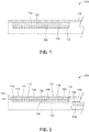
- FIGS. 1 and 2 illustrate a cross section view of a fingerprint sensor 100.
- a fingerprint sensor 100 can include a fingerprint sensor assembly, a cover glass assembly, and/or a fingerprint sensing mobile device. As illustrated in FIGS. 1 and 2 , the fingerprint sensor 100 can include a transmit layer 104, a sensor glass layer 108, a receive layer 112, and a protective cover layer 116.
- the transmit layer 104 (e.g., disposed on a first side of the sensor glass) can function to drive a strong electric field into the region above the receive layer 112.
- the transmit layer 104 can include a layer of indium tin oxide (ITO) rows. Indium tin oxide can serve as a good signal routing layer due to its electrical conductivity and optical transparency.
- ITO indium tin oxide
- indium tin oxide can be formed as a thin film.
- the indium tin oxide layer can be deposited using techniques such as physical vapor deposition, electron beam evaporation, and/or sputtering.
- the transmit layer 104 can include metal mesh, silver nanowires, and/or carbon nanotubes.
- the transmit layer 104 can be electrically coupled to a metal layer 106, which can be formed using techniques, such as lithography, deposition, and etching on a small scale, or other techniques such as placing wiring for a larger scale.
- the metal layer 106 can function to connect the supplies, inputs, and outputs of the controller 130 to the receive layer 112, transmit layer 104, or a flexible flat cable and/or a flexible printed circuit board.
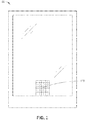
- the flexible printed circuit board and/or metal layer 106 can connect the controller 130 to a printed circuit board 138, for example. As represented in FIG. 2 , 138 can include a flexible printed circuit board and/or a printed circuit board.
- the controller 130 can detect the changes in mutual capacitance between the lines on the receive layer 112 and the lines on the transmit layer 104.
- the metal layer 106 can include any suitable conductive material, such as wires of copper, aluminum, etc.
- the fingerprint sensor 100 can include a sensor glass layer 108, as illustrated in FIGS. 1 and 2 .
- the sensor glass layer 108 can include a thin glass substrate configured to let light pass from a display assembly 102 through the fingerprint sensor 100 to a user while providing mechanical support.
- a sensor glass layer 108 thickness of about 400 microns can provide both strength and an adequate spatial modulation transfer function for the transmit layer 104. It is contemplated that the sensor glass layer 108 can be of varying thickness (e.g., 300 microns, 500 microns, etc.).
- the sensor glass layer 108 includes a thin glass substrate, such as an alkali-aluminosilicate sheet toughened glass manufactured through immersion in a molten alkaline salt bath using ion exchange to produce compressive residual stress at the surface.
- the sensor glass layer 108 can include soda-lime-silica glass. It is contemplated that other types of glass may also be utilized.
- the sensor glass layer 108 can be chosen and/or configured for breakage resistance. If additional strength is desired, the fingerprint sensor 100 can, in some embodiments, include at least one additional sensor glass layer 108.
- a second sensor glass layer 108 can be laminated between the transmit layer 104 and the metal layer 106 for additional strength.
- the transmit layer 104 can include a wiring pattern that includes a controller 130 in a chip-on-glass configuration and/or a ribbon cable configured to receive from and/or transmit signals to a motherboard or other device.
- the sensor glass layer 108 can include at least one through-glass via 110.
- a through-glass via 110 can include a through substrate via in the sensor glass layer 108.
- the through-glass via 110 can be backfilled with a conductive material, for example copper, or coated with a conductive material.
- the copper and/or conductive material can be electrically coupled to the transmit layer 104 and/or a receive layer 112.
- the at least one through-glass via 110 can include a metal-filled blind via that extends from the first side of the sensor glass layer 108 to the second side of the sensor glass layer 108, where the metal-filled blind via is configured to provide capacitive coupling between the transmit layer 104 and the receive layer 112.
- a blind via can include a via that is exposed on only one side of the sensor glass layer 108.
- the through-glass via 110 can be laser-drilled.
- the fingerprint sensor 100 can include multiple through-glass vias 110 disposed in a bezel area (e.g., the outer area and/or area proximate to the edge of the fingerprint sensor 100) that bring receive signals from the receive layer 112 to the transmit layer 104.
- Utilizing a through-glass via 110 can function to take leads from a transmit layer 104 on a first side of the sensor glass layer 108 to a receive layer 112 on a second side of the sensor glass layer 108 and eliminate flex cables and obviate awkward wiring on the receive layer 112 side (e.g., side of the sense glass 108 distal from the transmit layer 104) of the sensor glass layer 108. Bringing the receive signals from the receive layer 112 to the transmit layer 104 through the through-glass via(s) 110 provides a neater, thinner, and more compact assembly.
- the fingerprint sensor 100 can include a receive layer 112 disposed on the sensor glass layer 108.
- the receive layer 112 functions to sense the change in capacitance due to a fingerprint, touch, stylus, hovering finger, or gesturing hand.
- the receive layer 112 can include a transparent conductor, such as indium tin oxide (ITO), which can be patterned on the surface of the sensor glass layer 108.
- ITO indium tin oxide
- the receive layer 112 can be deposited using techniques such as physical vapor deposition, electron beam evaporation, and/or chemical vapor deposition.
- the receive layer 112 can be configured to route signals and/or provide electrical communication to and/or from the transmit layer 104 by way of at least one through-glass via 110.
- the fingerprint sensor 100 can include a protective cover layer 116 disposed on the receive layer 112 and sense glass layer 108.
- the protective cover layer 116 can include a protective layer and/or cover layer for the fingerprint sensor 100 and can be scratch-resistant as well as provide insulation for the receive layer 112.
- the protective cover layer 116 can include a thin single crystal layer, such as sapphire, which may be laminated on the receive layer 112 and the sensor glass layer 108. Sapphire is a hard natural material and can be difficult to scratch. Sapphire can function well as a protective cover layer 116.
- the single crystal sapphire layer can be approximately 100 ⁇ m to approximately 200 ⁇ m in thickness.
- the protective cover layer 116 can include a hard thin film.
- the protective cover layer 116 can include, for example, silicon nitride, aluminum oxide, silicon carbide, and/or diamond.
- a protective cover layer 116 includes a layer of aluminum oxide with a thickness of about one ⁇ m.
- a protective cover layer 116 including a hard thin film can be a conformal coating in full contact with the sensor glass layer 108 and/or the receive layer 112 (e.g., the indium tin oxide layer).
- the protective cover layer 116 may serve as a protective coating and/or an anti-reflective coating for the fingerprint sensor 100.
- the protective cover layer 116 functions as a touch surface upon which a user can use one or more fingers, a stylus, and so forth to input commands to the touch screen device 100.
- the protective cover layer 116 is an at least substantially transparent dielectric. Utilizing a thin protective cover layer 116 can allow the receive layer 112 to be disposed within several hundred microns, tens of microns, or even a few microns of a user's finger or stylus. The high dielectric constants of sapphire and/or the thin film further enhance sensitivity.
- the fingerprint sensor 100 may include a display assembly 102 (e.g., a liquid crystal display (LCD) and/or an organic light-emitting diode (OLED)).
- a display assembly 102 can include a display that employs the light modulating properties of liquid crystals.
- LCD displays can utilize two sheets of polarizing material with a liquid crystal solution between them. An electric current passed through the liquid causes the crystals to align so that light cannot pass through them. Each crystal functions as a shutter either allowing light to pass through or blocking the light.
- a display assembly 102 can include a video display, a flat panel display, an electronic visual display, a computer monitor, and/or an active-matrix organic light-emitting diode.
- a display assembly 102 can include an active-matrix organic light-emitting diode utilized in a smartphone or tablet computer.
- Some other examples of a display assembly 102 can include an electroluminescent display (ELD) or a plasma display panel.
- ELD electroluminescent display
- the fingerprint sensor 100 can include a display assembly 102 (e.g., a liquid crystal display) with a sensor glass layer 108 disposed on the display assembly 102.
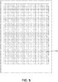
- a receive layer 112 and a transmit layer 104 can be patterned into a first layer 122 (e.g., a single indium tin oxide layer including the receive layer 112 and the transmit layer 104) on the sensor glass layer 108 with conductive bridge(s) 118 formed in a second layer 124 of indium tin oxide (or other suitable material).
- the first layer 122 can be physically and/or electrically separated from the second layer 124 by at least one dielectric patch 120 (e.g., a thin-film patch) at each row/column intersection, which can make the columns of the receive layer 112 continuous.
- the fingerprint sensor 100 can sense touch, styli, hover, and gestures. This is done by electrically ganging the transmit layer 104 (e.g., transmit rows) and also ganging the receive layer 112 (e.g., receive columns) to form wider sensing elements.
- the fingerprint sensing portion 103 can be limited to a small area of the fingerprint sensor 100 and protective cover layer 116.
- an example 1 cm 2 fingerprint sense area may provide adequate fingerprint sensing with a pitch of 50 microns, which can require about 200 transmit lines and about 200 receive lines. Each of these lines can be electrically and/or physically connected to a contact pad on a controller 130.
- the fingerprint sensing portion 103 of an overall device can include a larger portion of the entire cover glass device, such as the touch-panel device shown in FIG. 5 .
- a larger area fingerprint sensor 100 may enable expanded functionality.
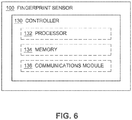
- the fingerprint sensor 100 can include a controller 130 configured to authenticate a user.
- the controller 130 may further include a processor 132, a communications module 136, and/or memory 134.
- the processor 132 can provide processing functionality for the controller 130 and may include any number of processors, micro-controllers, or other processing systems and resident or external memory for storing data and other information accessed or generated by the controller 130.
- the processor may execute one or more software programs, such as a fingerprint sensing application, which implement techniques described herein.
- the processor 132 is not limited by the materials from which it is formed or the processing mechanisms employed therein, and as such, may be implemented via semiconductor(s) and/or transistors (e.g., using electronic integrated circuit (IC) components), and so forth.
- the communications module 136 can be operatively configured to communicate with components of the fingerprint sensor 100 and/or system host.
- the communications module 136 can also be communicatively coupled with the processor 132 (e.g., for communicating inputs from the fingerprint sensor 100 to the processor 132).
- the communications module 136 and/or the processor 132 can also be configured to communicate with a variety of different networks, including the Internet, a cellular telephone network, a local area network (LAN), a wide area network (WAN), a wireless network, a public telephone network, and/or an intranet, for example.
- the communications module 136 can include sensing lines between components of the fingerprint sensor 100.
- the memory 134 is an example of tangible computer-readable media that provides storage functionality to store various data associated with operation of the controller 130, such as software programs and/or code segments, algorithms, or other data to instruct the processor 132 and/or other components of the controller 130 to perform the steps and/or functions described herein.
- the memory 134 can store data, such as a program of instructions for operating a fingerprint sensor 100 (including its components), data, and so on.
- a single memory 134 is described, a wide variety of types and combinations of memory (e.g., tangible memory, non-transitory) may be employed.
- the memory 134 may be integral with the processor 132, may comprise stand-alone memory, or may be a combination of both.
- the memory 134 may include removable and non-removable memory components, such as Random Access Memory (RAM), Read-Only Memory (ROM), Flash memory (e.g., a Secure Digital (SD) memory card, a mini-SD memory card, and/or a micro-SD memory card), magnetic memory, optical memory, a Universal Serial Bus (USB) memory device, hard disk memory, external memory, and other types of computer-readable storage media.
- RAM Random Access Memory
- ROM Read-Only Memory
- Flash memory e.g., a Secure Digital (SD) memory card, a mini-SD memory card, and/or a micro-SD memory card
- magnetic memory e.g., a Secure Digital (SD) memory card, a mini-SD memory card, and/or a micro-SD memory card
- magnetic memory e.g., a Secure Digital (SD) memory card, a mini-SD memory card, and/or a micro-SD memory card
- USB Universal Serial Bus
- the fingerprint sensor 100 and/or memory 134 may include removable
Landscapes
- Engineering & Computer Science (AREA)
- Physics & Mathematics (AREA)
- General Physics & Mathematics (AREA)
- Theoretical Computer Science (AREA)
- Human Computer Interaction (AREA)
- Multimedia (AREA)
- General Engineering & Computer Science (AREA)
- Image Input (AREA)
- Measurement Of Length, Angles, Or The Like Using Electric Or Magnetic Means (AREA)
- Measurement Of The Respiration, Hearing Ability, Form, And Blood Characteristics Of Living Organisms (AREA)
Applications Claiming Priority (3)
| Application Number | Priority Date | Filing Date | Title |
|---|---|---|---|
| US201462028887P | 2014-07-25 | 2014-07-25 | |
| US14/496,073 US9558390B2 (en) | 2014-07-25 | 2014-09-25 | High-resolution electric field sensor in cover glass |
| PCT/US2015/041522 WO2016014660A1 (en) | 2014-07-25 | 2015-07-22 | High-resolution electric field sensor in cover glass |
Publications (2)
| Publication Number | Publication Date |
|---|---|
| EP3172694A1 EP3172694A1 (en) | 2017-05-31 |
| EP3172694B1 true EP3172694B1 (en) | 2021-06-02 |
Family
ID=53773564
Family Applications (1)
| Application Number | Title | Priority Date | Filing Date |
|---|---|---|---|
| EP15745343.2A Active EP3172694B1 (en) | 2014-07-25 | 2015-07-22 | High-resolution electric field sensor in cover glass |
Country Status (6)
| Country | Link |
|---|---|
| US (2) | US9558390B2 (enExample) |
| EP (1) | EP3172694B1 (enExample) |
| JP (1) | JP2017521797A (enExample) |
| KR (1) | KR20170036687A (enExample) |
| CN (1) | CN106663194B (enExample) |
| WO (1) | WO2016014660A1 (enExample) |
Families Citing this family (36)
| Publication number | Priority date | Publication date | Assignee | Title |
|---|---|---|---|---|
| JP5884764B2 (ja) * | 2013-03-29 | 2016-03-15 | ブラザー工業株式会社 | 通信装置、およびプログラム |
| US10036734B2 (en) | 2013-06-03 | 2018-07-31 | Snaptrack, Inc. | Ultrasonic sensor with bonded piezoelectric layer |
| US20140355387A1 (en) | 2013-06-03 | 2014-12-04 | Qualcomm Incorporated | Ultrasonic receiver with coated piezoelectric layer |
| US9558390B2 (en) | 2014-07-25 | 2017-01-31 | Qualcomm Incorporated | High-resolution electric field sensor in cover glass |
| CN104766053B (zh) * | 2015-03-26 | 2018-10-30 | 业成光电(深圳)有限公司 | 指纹识别装置及其制造方法 |
| US20170103249A1 (en) | 2015-10-09 | 2017-04-13 | Corning Incorporated | Glass-based substrate with vias and process of forming the same |
| US10282585B2 (en) | 2015-11-13 | 2019-05-07 | Cypress Semiconductor Corporation | Sensor-compatible overlay |
| US9639734B1 (en) | 2015-11-13 | 2017-05-02 | Cypress Semiconductor Corporation | Fingerprint sensor-compatible overlay material |
| US10832029B2 (en) | 2015-11-13 | 2020-11-10 | Cypress Semiconductor Corporation | Sensor-compatible overlay |
| US9773153B1 (en) * | 2016-03-24 | 2017-09-26 | Fingerprint Cards Ab | Fingerprint sensor module |
| US20170285778A1 (en) * | 2016-04-01 | 2017-10-05 | Intel Corporation | Electronic device with fingerprint sensor |
| US10410883B2 (en) | 2016-06-01 | 2019-09-10 | Corning Incorporated | Articles and methods of forming vias in substrates |
| US11003884B2 (en) | 2016-06-16 | 2021-05-11 | Qualcomm Incorporated | Fingerprint sensor device and methods thereof |
| JP6934079B2 (ja) * | 2016-06-27 | 2021-09-08 | 株式会社ジャパンディスプレイ | 表示装置 |
| JP6684167B2 (ja) | 2016-06-27 | 2020-04-22 | 株式会社ジャパンディスプレイ | 表示装置 |
| US10794679B2 (en) | 2016-06-29 | 2020-10-06 | Corning Incorporated | Method and system for measuring geometric parameters of through holes |
| US10134657B2 (en) | 2016-06-29 | 2018-11-20 | Corning Incorporated | Inorganic wafer having through-holes attached to semiconductor wafer |
| CN106095211B (zh) * | 2016-06-30 | 2019-06-18 | 京东方科技集团股份有限公司 | 显示面板及其制备方法、显示装置 |
| JP6651420B2 (ja) | 2016-07-11 | 2020-02-19 | 株式会社ジャパンディスプレイ | カバー部材及び表示装置 |
| CN106354351B (zh) * | 2016-08-30 | 2019-04-05 | 京东方科技集团股份有限公司 | 触控基板及制作方法、显示装置、指纹识别装置和方法 |
| CN106127195B (zh) * | 2016-08-30 | 2017-11-17 | 广东欧珀移动通信有限公司 | 指纹模组、指纹模组制作方法及移动终端 |
| TW201815710A (zh) * | 2016-08-31 | 2018-05-01 | 美商康寧公司 | 具有經填充之孔洞的經強化玻璃系物件及製造其之方法 |
| US10984304B2 (en) | 2017-02-02 | 2021-04-20 | Jonny B. Vu | Methods for placing an EMV chip onto a metal card |
| US11078112B2 (en) | 2017-05-25 | 2021-08-03 | Corning Incorporated | Silica-containing substrates with vias having an axially variable sidewall taper and methods for forming the same |
| US10580725B2 (en) | 2017-05-25 | 2020-03-03 | Corning Incorporated | Articles having vias with geometry attributes and methods for fabricating the same |
| TWI633480B (zh) * | 2017-08-07 | 2018-08-21 | 致伸科技股份有限公司 | 指紋辨識觸控屏 |
| US12180108B2 (en) | 2017-12-19 | 2024-12-31 | Corning Incorporated | Methods for etching vias in glass-based articles employing positive charge organic molecules |
| US11554984B2 (en) | 2018-02-22 | 2023-01-17 | Corning Incorporated | Alkali-free borosilicate glasses with low post-HF etch roughness |
| US11152294B2 (en) | 2018-04-09 | 2021-10-19 | Corning Incorporated | Hermetic metallized via with improved reliability |
| USD956760S1 (en) * | 2018-07-30 | 2022-07-05 | Lion Credit Card Inc. | Multi EMV chip card |
| US12200875B2 (en) | 2018-09-20 | 2025-01-14 | Industrial Technology Research Institute | Copper metallization for through-glass vias on thin glass |
| CN112070018B (zh) | 2018-12-14 | 2023-12-01 | 深圳市汇顶科技股份有限公司 | 指纹识别装置和电子设备 |
| KR20250083587A (ko) | 2019-02-21 | 2025-06-10 | 코닝 인코포레이티드 | 구리-금속화된 쓰루 홀을 갖는 유리 또는 유리 세라믹 물품 및 이를 제조하기 위한 공정 |
| KR102697765B1 (ko) * | 2019-05-15 | 2024-08-21 | 삼성전자주식회사 | 지문 센서, 지문 센서 어레이 및 장치 |
| WO2021041037A1 (en) * | 2019-08-30 | 2021-03-04 | Corning Incorporated | Display protector assemblies having vias |
| CN117030599A (zh) * | 2023-08-11 | 2023-11-10 | 吉林大学 | 一种便捷式模具毛刺锐角识别防划伤装置 |
Family Cites Families (27)
| Publication number | Priority date | Publication date | Assignee | Title |
|---|---|---|---|---|
| JPS5368180A (en) * | 1976-11-30 | 1978-06-17 | Nippon Telegr & Teleph Corp <Ntt> | Semiconductor device |
| JP2001111233A (ja) * | 1999-10-07 | 2001-04-20 | Mitsubishi Gas Chem Co Inc | フリップチップ搭載用高密度多層プリント配線板 |
| NO316796B1 (no) * | 2002-03-01 | 2004-05-10 | Idex Asa | Sensormodul for maling av strukturer i en overflate, saerlig en fingeroverflate |
| WO2003102974A1 (fr) * | 2002-06-03 | 2003-12-11 | Mitsubishi Denki Kabushiki Kaisha | Pellicule fine de platine et capteur thermique |
| FI20030102A0 (fi) * | 2003-01-22 | 2003-01-22 | Nokia Corp | Henkilön varmennusjärjestely |
| JP2006061630A (ja) * | 2004-08-30 | 2006-03-09 | Glory Ltd | 指紋検出装置および指紋検出装置の製造方法 |
| TWI310521B (en) * | 2005-06-29 | 2009-06-01 | Egis Technology Inc | Structure of sweep-type fingerprint sensing chip capable of resisting electrostatic discharge (esd) and method of fabricating the same |
| US7714882B2 (en) * | 2006-09-15 | 2010-05-11 | Ricoh Company, Ltd. | Image forming apparatus and image forming process |
| US8610690B2 (en) * | 2007-07-27 | 2013-12-17 | Tpk Touch Solutions Inc. | Capacitive sensor and method for manufacturing same |
| US8470680B2 (en) * | 2008-07-28 | 2013-06-25 | Kemet Electronics Corporation | Substrate with embedded patterned capacitance |
| JP5230533B2 (ja) * | 2009-05-29 | 2013-07-10 | 三菱電機株式会社 | タッチパネルおよびそれを備えた表示装置 |
| US9274553B2 (en) | 2009-10-30 | 2016-03-01 | Synaptics Incorporated | Fingerprint sensor and integratable electronic display |
| NO20093601A1 (no) * | 2009-12-29 | 2011-06-30 | Idex Asa | Overflatesensor |
| US8866347B2 (en) | 2010-01-15 | 2014-10-21 | Idex Asa | Biometric image sensing |
| US8724038B2 (en) * | 2010-10-18 | 2014-05-13 | Qualcomm Mems Technologies, Inc. | Wraparound assembly for combination touch, handwriting and fingerprint sensor |
| US8564314B2 (en) * | 2010-11-02 | 2013-10-22 | Atmel Corporation | Capacitive touch sensor for identifying a fingerprint |
| US9310940B2 (en) | 2011-01-17 | 2016-04-12 | Pixart Imaging Inc. | Capacitive touchscreen or touch panel with fingerprint reader |
| US8884502B2 (en) * | 2011-07-25 | 2014-11-11 | General Electric Company | OLED assembly and luminaire with removable diffuser |
| JP5849344B2 (ja) * | 2011-08-09 | 2016-01-27 | 日本電気株式会社 | 位置検出装置 |
| US20130265137A1 (en) | 2012-04-02 | 2013-10-10 | Validity Sensors, Inc. | Integratable fingerprint sensor packagings |
| US20130287274A1 (en) | 2012-04-29 | 2013-10-31 | Weidong Shi | Methods and Apparatuses of Unified Capacitive Based Sensing of Touch and Fingerprint |
| US20140062875A1 (en) * | 2012-09-06 | 2014-03-06 | Panasonic Corporation | Mobile device with an inertial measurement unit to adjust state of graphical user interface or a natural language processing unit, and including a hover sensing function |
| US9250753B2 (en) * | 2013-01-07 | 2016-02-02 | Microsoft Technology Licensing, Llc | Capacitive touch surface in close proximity to display |
| US20150009118A1 (en) * | 2013-07-03 | 2015-01-08 | Nvidia Corporation | Intelligent page turner and scroller |
| US9177831B2 (en) * | 2013-09-30 | 2015-11-03 | Intel Corporation | Die assembly on thin dielectric sheet |
| US9342727B2 (en) * | 2014-03-04 | 2016-05-17 | Apple Inc. | Field shaping channels in a substrate above a biometric sensing device |
| US9558390B2 (en) | 2014-07-25 | 2017-01-31 | Qualcomm Incorporated | High-resolution electric field sensor in cover glass |
-
2014
- 2014-09-25 US US14/496,073 patent/US9558390B2/en not_active Expired - Fee Related
-
2015
- 2015-07-22 JP JP2017503482A patent/JP2017521797A/ja active Pending
- 2015-07-22 KR KR1020177001888A patent/KR20170036687A/ko not_active Withdrawn
- 2015-07-22 CN CN201580038985.XA patent/CN106663194B/zh not_active Expired - Fee Related
- 2015-07-22 WO PCT/US2015/041522 patent/WO2016014660A1/en not_active Ceased
- 2015-07-22 EP EP15745343.2A patent/EP3172694B1/en active Active
-
2016
- 2016-12-14 US US15/378,897 patent/US10268864B2/en active Active
Non-Patent Citations (1)
| Title |
|---|
| EDN JUNE: "Sensor Ganging - Optimize power in a capacitive sensing system - Part I", 1 January 2015 (2015-01-01), XP055764455, Retrieved from the Internet <URL:edn.com/sensor-ganging-optimize-power-in-a-capacitive-sensing-system-part-i> [retrieved on 20210111] * |
Also Published As
| Publication number | Publication date |
|---|---|
| JP2017521797A (ja) | 2017-08-03 |
| CN106663194B (zh) | 2019-06-18 |
| CN106663194A (zh) | 2017-05-10 |
| US20160026842A1 (en) | 2016-01-28 |
| EP3172694A1 (en) | 2017-05-31 |
| WO2016014660A1 (en) | 2016-01-28 |
| US9558390B2 (en) | 2017-01-31 |
| KR20170036687A (ko) | 2017-04-03 |
| US10268864B2 (en) | 2019-04-23 |
| US20170091513A1 (en) | 2017-03-30 |
Similar Documents
| Publication | Publication Date | Title |
|---|---|---|
| EP3172694B1 (en) | High-resolution electric field sensor in cover glass | |
| TWI522932B (zh) | 電容性感測器、裝置及方法 | |
| US8603574B2 (en) | Curved touch sensor | |
| US7030860B1 (en) | Flexible transparent touch sensing system for electronic devices | |
| US9104283B2 (en) | Capacitive detection device with arrangement of linking tracks, and method implementing such a device | |
| US10613689B2 (en) | Touch screen, method of manufacturing touch screen, and display device including touch screen | |
| KR102618537B1 (ko) | 온-스크린 지문 센서 및 이를 포함하는 전자 기기 | |
| US20140132854A1 (en) | Touch display device | |
| WO2016040468A1 (en) | Device and method for force and proximity sensing employing an intermediate shield electrode layer | |
| US10754478B2 (en) | Capacitive display device | |
| EP3101591A1 (en) | Terminal for recognizing fingerprint | |
| US9372587B2 (en) | Methods and apparatus for arranging electrode layers and associated routing traces in a sensor device | |
| US10572707B2 (en) | Transparent fingerprint sensor pattern | |
| CN115437524A (zh) | 用于具有屏蔽的跨电容性感测的传感器设备 | |
| CN105320327A (zh) | 手持式电子装置及其触控外盖 | |
| US20190302941A1 (en) | Touchscreen, Method for Touch Detection, and Wearable Device | |
| CN105302386A (zh) | 无挡触控的手持式电子装置及其触控外盖 | |
| CN105302349A (zh) | 无挡触控的手持式电子装置及其触控外盖 | |
| TWM448739U (zh) | 電磁感應天線基板、結合電容式觸控與電磁式感應的複合基板、電磁輸入裝置及具觸控與書寫輸入功能之裝置 | |
| WO2017031764A1 (en) | Apparatus and method for an rfid touch panel |
Legal Events
| Date | Code | Title | Description |
|---|---|---|---|
| STAA | Information on the status of an ep patent application or granted ep patent |
Free format text: STATUS: THE INTERNATIONAL PUBLICATION HAS BEEN MADE |
|
| PUAI | Public reference made under article 153(3) epc to a published international application that has entered the european phase |
Free format text: ORIGINAL CODE: 0009012 |
|
| STAA | Information on the status of an ep patent application or granted ep patent |
Free format text: STATUS: REQUEST FOR EXAMINATION WAS MADE |
|
| 17P | Request for examination filed |
Effective date: 20161209 |
|
| AK | Designated contracting states |
Kind code of ref document: A1 Designated state(s): AL AT BE BG CH CY CZ DE DK EE ES FI FR GB GR HR HU IE IS IT LI LT LU LV MC MK MT NL NO PL PT RO RS SE SI SK SM TR |
|
| AX | Request for extension of the european patent |
Extension state: BA ME |
|
| DAV | Request for validation of the european patent (deleted) | ||
| DAX | Request for extension of the european patent (deleted) | ||
| STAA | Information on the status of an ep patent application or granted ep patent |
Free format text: STATUS: EXAMINATION IS IN PROGRESS |
|
| 17Q | First examination report despatched |
Effective date: 20180103 |
|
| GRAP | Despatch of communication of intention to grant a patent |
Free format text: ORIGINAL CODE: EPIDOSNIGR1 |
|
| STAA | Information on the status of an ep patent application or granted ep patent |
Free format text: STATUS: GRANT OF PATENT IS INTENDED |
|
| INTG | Intention to grant announced |
Effective date: 20210202 |
|
| GRAS | Grant fee paid |
Free format text: ORIGINAL CODE: EPIDOSNIGR3 |
|
| GRAA | (expected) grant |
Free format text: ORIGINAL CODE: 0009210 |
|
| STAA | Information on the status of an ep patent application or granted ep patent |
Free format text: STATUS: THE PATENT HAS BEEN GRANTED |
|
| REG | Reference to a national code |
Ref country code: CH Ref legal event code: EP |
|
| AK | Designated contracting states |
Kind code of ref document: B1 Designated state(s): AL AT BE BG CH CY CZ DE DK EE ES FI FR GB GR HR HU IE IS IT LI LT LU LV MC MK MT NL NO PL PT RO RS SE SI SK SM TR |
|
| REG | Reference to a national code |
Ref country code: GB Ref legal event code: FG4D |
|
| REG | Reference to a national code |
Ref country code: AT Ref legal event code: REF Ref document number: 1399134 Country of ref document: AT Kind code of ref document: T Effective date: 20210615 |
|
| REG | Reference to a national code |
Ref country code: IE Ref legal event code: FG4D |
|
| REG | Reference to a national code |
Ref country code: DE Ref legal event code: R096 Ref document number: 602015069986 Country of ref document: DE |
|
| REG | Reference to a national code |
Ref country code: LT Ref legal event code: MG9D |
|
| PG25 | Lapsed in a contracting state [announced via postgrant information from national office to epo] |
Ref country code: HR Free format text: LAPSE BECAUSE OF FAILURE TO SUBMIT A TRANSLATION OF THE DESCRIPTION OR TO PAY THE FEE WITHIN THE PRESCRIBED TIME-LIMIT Effective date: 20210602 Ref country code: BG Free format text: LAPSE BECAUSE OF FAILURE TO SUBMIT A TRANSLATION OF THE DESCRIPTION OR TO PAY THE FEE WITHIN THE PRESCRIBED TIME-LIMIT Effective date: 20210902 Ref country code: LT Free format text: LAPSE BECAUSE OF FAILURE TO SUBMIT A TRANSLATION OF THE DESCRIPTION OR TO PAY THE FEE WITHIN THE PRESCRIBED TIME-LIMIT Effective date: 20210602 Ref country code: FI Free format text: LAPSE BECAUSE OF FAILURE TO SUBMIT A TRANSLATION OF THE DESCRIPTION OR TO PAY THE FEE WITHIN THE PRESCRIBED TIME-LIMIT Effective date: 20210602 |
|
| REG | Reference to a national code |
Ref country code: NL Ref legal event code: MP Effective date: 20210602 |
|
| REG | Reference to a national code |
Ref country code: AT Ref legal event code: MK05 Ref document number: 1399134 Country of ref document: AT Kind code of ref document: T Effective date: 20210602 |
|
| REG | Reference to a national code |
Ref country code: DE Ref legal event code: R079 Ref document number: 602015069986 Country of ref document: DE Free format text: PREVIOUS MAIN CLASS: G06K0009000000 Ipc: G06V0010000000 |
|
| PG25 | Lapsed in a contracting state [announced via postgrant information from national office to epo] |
Ref country code: PL Free format text: LAPSE BECAUSE OF FAILURE TO SUBMIT A TRANSLATION OF THE DESCRIPTION OR TO PAY THE FEE WITHIN THE PRESCRIBED TIME-LIMIT Effective date: 20210602 Ref country code: NO Free format text: LAPSE BECAUSE OF FAILURE TO SUBMIT A TRANSLATION OF THE DESCRIPTION OR TO PAY THE FEE WITHIN THE PRESCRIBED TIME-LIMIT Effective date: 20210902 Ref country code: SE Free format text: LAPSE BECAUSE OF FAILURE TO SUBMIT A TRANSLATION OF THE DESCRIPTION OR TO PAY THE FEE WITHIN THE PRESCRIBED TIME-LIMIT Effective date: 20210602 Ref country code: RS Free format text: LAPSE BECAUSE OF FAILURE TO SUBMIT A TRANSLATION OF THE DESCRIPTION OR TO PAY THE FEE WITHIN THE PRESCRIBED TIME-LIMIT Effective date: 20210602 Ref country code: LV Free format text: LAPSE BECAUSE OF FAILURE TO SUBMIT A TRANSLATION OF THE DESCRIPTION OR TO PAY THE FEE WITHIN THE PRESCRIBED TIME-LIMIT Effective date: 20210602 Ref country code: GR Free format text: LAPSE BECAUSE OF FAILURE TO SUBMIT A TRANSLATION OF THE DESCRIPTION OR TO PAY THE FEE WITHIN THE PRESCRIBED TIME-LIMIT Effective date: 20210903 |
|
| PG25 | Lapsed in a contracting state [announced via postgrant information from national office to epo] |
Ref country code: CZ Free format text: LAPSE BECAUSE OF FAILURE TO SUBMIT A TRANSLATION OF THE DESCRIPTION OR TO PAY THE FEE WITHIN THE PRESCRIBED TIME-LIMIT Effective date: 20210602 Ref country code: EE Free format text: LAPSE BECAUSE OF FAILURE TO SUBMIT A TRANSLATION OF THE DESCRIPTION OR TO PAY THE FEE WITHIN THE PRESCRIBED TIME-LIMIT Effective date: 20210602 Ref country code: SK Free format text: LAPSE BECAUSE OF FAILURE TO SUBMIT A TRANSLATION OF THE DESCRIPTION OR TO PAY THE FEE WITHIN THE PRESCRIBED TIME-LIMIT Effective date: 20210602 Ref country code: SM Free format text: LAPSE BECAUSE OF FAILURE TO SUBMIT A TRANSLATION OF THE DESCRIPTION OR TO PAY THE FEE WITHIN THE PRESCRIBED TIME-LIMIT Effective date: 20210602 Ref country code: AT Free format text: LAPSE BECAUSE OF FAILURE TO SUBMIT A TRANSLATION OF THE DESCRIPTION OR TO PAY THE FEE WITHIN THE PRESCRIBED TIME-LIMIT Effective date: 20210602 Ref country code: PT Free format text: LAPSE BECAUSE OF FAILURE TO SUBMIT A TRANSLATION OF THE DESCRIPTION OR TO PAY THE FEE WITHIN THE PRESCRIBED TIME-LIMIT Effective date: 20211004 Ref country code: NL Free format text: LAPSE BECAUSE OF FAILURE TO SUBMIT A TRANSLATION OF THE DESCRIPTION OR TO PAY THE FEE WITHIN THE PRESCRIBED TIME-LIMIT Effective date: 20210602 Ref country code: RO Free format text: LAPSE BECAUSE OF FAILURE TO SUBMIT A TRANSLATION OF THE DESCRIPTION OR TO PAY THE FEE WITHIN THE PRESCRIBED TIME-LIMIT Effective date: 20210602 Ref country code: ES Free format text: LAPSE BECAUSE OF FAILURE TO SUBMIT A TRANSLATION OF THE DESCRIPTION OR TO PAY THE FEE WITHIN THE PRESCRIBED TIME-LIMIT Effective date: 20210602 |
|
| REG | Reference to a national code |
Ref country code: CH Ref legal event code: PL |
|
| REG | Reference to a national code |
Ref country code: DE Ref legal event code: R097 Ref document number: 602015069986 Country of ref document: DE |
|
| PG25 | Lapsed in a contracting state [announced via postgrant information from national office to epo] |
Ref country code: MC Free format text: LAPSE BECAUSE OF FAILURE TO SUBMIT A TRANSLATION OF THE DESCRIPTION OR TO PAY THE FEE WITHIN THE PRESCRIBED TIME-LIMIT Effective date: 20210602 |
|
| REG | Reference to a national code |
Ref country code: BE Ref legal event code: MM Effective date: 20210731 |
|
| PLBE | No opposition filed within time limit |
Free format text: ORIGINAL CODE: 0009261 |
|
| STAA | Information on the status of an ep patent application or granted ep patent |
Free format text: STATUS: NO OPPOSITION FILED WITHIN TIME LIMIT |
|
| PG25 | Lapsed in a contracting state [announced via postgrant information from national office to epo] |
Ref country code: LI Free format text: LAPSE BECAUSE OF NON-PAYMENT OF DUE FEES Effective date: 20210731 Ref country code: DK Free format text: LAPSE BECAUSE OF FAILURE TO SUBMIT A TRANSLATION OF THE DESCRIPTION OR TO PAY THE FEE WITHIN THE PRESCRIBED TIME-LIMIT Effective date: 20210602 Ref country code: CH Free format text: LAPSE BECAUSE OF NON-PAYMENT OF DUE FEES Effective date: 20210731 |
|
| 26N | No opposition filed |
Effective date: 20220303 |
|
| PG25 | Lapsed in a contracting state [announced via postgrant information from national office to epo] |
Ref country code: LU Free format text: LAPSE BECAUSE OF NON-PAYMENT OF DUE FEES Effective date: 20210722 Ref country code: AL Free format text: LAPSE BECAUSE OF FAILURE TO SUBMIT A TRANSLATION OF THE DESCRIPTION OR TO PAY THE FEE WITHIN THE PRESCRIBED TIME-LIMIT Effective date: 20210602 |
|
| PG25 | Lapsed in a contracting state [announced via postgrant information from national office to epo] |
Ref country code: IT Free format text: LAPSE BECAUSE OF FAILURE TO SUBMIT A TRANSLATION OF THE DESCRIPTION OR TO PAY THE FEE WITHIN THE PRESCRIBED TIME-LIMIT Effective date: 20210602 Ref country code: IE Free format text: LAPSE BECAUSE OF NON-PAYMENT OF DUE FEES Effective date: 20210722 Ref country code: BE Free format text: LAPSE BECAUSE OF NON-PAYMENT OF DUE FEES Effective date: 20210731 |
|
| PG25 | Lapsed in a contracting state [announced via postgrant information from national office to epo] |
Ref country code: HU Free format text: LAPSE BECAUSE OF FAILURE TO SUBMIT A TRANSLATION OF THE DESCRIPTION OR TO PAY THE FEE WITHIN THE PRESCRIBED TIME-LIMIT; INVALID AB INITIO Effective date: 20150722 |
|
| PG25 | Lapsed in a contracting state [announced via postgrant information from national office to epo] |
Ref country code: CY Free format text: LAPSE BECAUSE OF FAILURE TO SUBMIT A TRANSLATION OF THE DESCRIPTION OR TO PAY THE FEE WITHIN THE PRESCRIBED TIME-LIMIT Effective date: 20210602 |
|
| PGFP | Annual fee paid to national office [announced via postgrant information from national office to epo] |
Ref country code: FR Payment date: 20230616 Year of fee payment: 9 |
|
| PGFP | Annual fee paid to national office [announced via postgrant information from national office to epo] |
Ref country code: GB Payment date: 20230614 Year of fee payment: 9 |
|
| PGFP | Annual fee paid to national office [announced via postgrant information from national office to epo] |
Ref country code: DE Payment date: 20230614 Year of fee payment: 9 |
|
| PG25 | Lapsed in a contracting state [announced via postgrant information from national office to epo] |
Ref country code: MK Free format text: LAPSE BECAUSE OF FAILURE TO SUBMIT A TRANSLATION OF THE DESCRIPTION OR TO PAY THE FEE WITHIN THE PRESCRIBED TIME-LIMIT Effective date: 20210602 |
|
| PG25 | Lapsed in a contracting state [announced via postgrant information from national office to epo] |
Ref country code: MT Free format text: LAPSE BECAUSE OF FAILURE TO SUBMIT A TRANSLATION OF THE DESCRIPTION OR TO PAY THE FEE WITHIN THE PRESCRIBED TIME-LIMIT Effective date: 20210602 |
|
| REG | Reference to a national code |
Ref country code: DE Ref legal event code: R119 Ref document number: 602015069986 Country of ref document: DE |
|
| GBPC | Gb: european patent ceased through non-payment of renewal fee |
Effective date: 20240722 |
|
| PG25 | Lapsed in a contracting state [announced via postgrant information from national office to epo] |
Ref country code: DE Free format text: LAPSE BECAUSE OF NON-PAYMENT OF DUE FEES Effective date: 20250201 |
|
| PG25 | Lapsed in a contracting state [announced via postgrant information from national office to epo] |
Ref country code: FR Free format text: LAPSE BECAUSE OF NON-PAYMENT OF DUE FEES Effective date: 20240731 |
|
| PG25 | Lapsed in a contracting state [announced via postgrant information from national office to epo] |
Ref country code: GB Free format text: LAPSE BECAUSE OF NON-PAYMENT OF DUE FEES Effective date: 20240722 |
|
| PG25 | Lapsed in a contracting state [announced via postgrant information from national office to epo] |
Ref country code: TR Free format text: LAPSE BECAUSE OF FAILURE TO SUBMIT A TRANSLATION OF THE DESCRIPTION OR TO PAY THE FEE WITHIN THE PRESCRIBED TIME-LIMIT Effective date: 20210602 |