EP3167992B1 - Bleilötverbindungsstruktur und verfahren zu ihrer herstellung - Google Patents
Bleilötverbindungsstruktur und verfahren zu ihrer herstellung Download PDFInfo
- Publication number
- EP3167992B1 EP3167992B1 EP16187779.0A EP16187779A EP3167992B1 EP 3167992 B1 EP3167992 B1 EP 3167992B1 EP 16187779 A EP16187779 A EP 16187779A EP 3167992 B1 EP3167992 B1 EP 3167992B1
- Authority
- EP
- European Patent Office
- Prior art keywords
- solder layer
- solder
- lead
- layer
- joint
- Prior art date
- Legal status (The legal status is an assumption and is not a legal conclusion. Google has not performed a legal analysis and makes no representation as to the accuracy of the status listed.)
- Active
Links
- 229910000679 solder Inorganic materials 0.000 title claims description 122
- 238000004519 manufacturing process Methods 0.000 title claims description 12
- 238000000034 method Methods 0.000 claims description 39
- 229910000765 intermetallic Inorganic materials 0.000 claims description 36
- 230000008569 process Effects 0.000 claims description 26
- 239000000470 constituent Substances 0.000 claims description 13
- 229910052709 silver Inorganic materials 0.000 claims description 12
- 238000005476 soldering Methods 0.000 claims description 10
- 239000004332 silver Substances 0.000 claims description 9
- RYGMFSIKBFXOCR-UHFFFAOYSA-N Copper Chemical compound [Cu] RYGMFSIKBFXOCR-UHFFFAOYSA-N 0.000 claims description 5
- QCEUXSAXTBNJGO-UHFFFAOYSA-N [Ag].[Sn] Chemical compound [Ag].[Sn] QCEUXSAXTBNJGO-UHFFFAOYSA-N 0.000 claims description 5
- KUNSUQLRTQLHQQ-UHFFFAOYSA-N copper tin Chemical compound [Cu].[Sn] KUNSUQLRTQLHQQ-UHFFFAOYSA-N 0.000 claims description 5
- 238000005304 joining Methods 0.000 claims description 4
- 238000010438 heat treatment Methods 0.000 claims description 2
- ATJFFYVFTNAWJD-UHFFFAOYSA-N Tin Chemical compound [Sn] ATJFFYVFTNAWJD-UHFFFAOYSA-N 0.000 description 19
- 239000004020 conductor Substances 0.000 description 15
- 238000010586 diagram Methods 0.000 description 8
- 238000002844 melting Methods 0.000 description 8
- 230000008018 melting Effects 0.000 description 8
- 229910000978 Pb alloy Inorganic materials 0.000 description 5
- 239000000463 material Substances 0.000 description 5
- 238000005219 brazing Methods 0.000 description 4
- 230000015556 catabolic process Effects 0.000 description 4
- 238000006731 degradation reaction Methods 0.000 description 4
- 229910045601 alloy Inorganic materials 0.000 description 3
- 239000000956 alloy Substances 0.000 description 3
- 229910052751 metal Inorganic materials 0.000 description 3
- 239000002184 metal Substances 0.000 description 3
- 229910001128 Sn alloy Inorganic materials 0.000 description 2
- 239000000853 adhesive Substances 0.000 description 2
- 230000001070 adhesive effect Effects 0.000 description 2
- 229910052782 aluminium Inorganic materials 0.000 description 2
- XAGFODPZIPBFFR-UHFFFAOYSA-N aluminium Chemical compound [Al] XAGFODPZIPBFFR-UHFFFAOYSA-N 0.000 description 2
- 229910052802 copper Inorganic materials 0.000 description 2
- 239000010949 copper Substances 0.000 description 2
- 230000008642 heat stress Effects 0.000 description 2
- 229910000833 kovar Inorganic materials 0.000 description 2
- 229910052745 lead Inorganic materials 0.000 description 2
- LQBJWKCYZGMFEV-UHFFFAOYSA-N lead tin Chemical compound [Sn].[Pb] LQBJWKCYZGMFEV-UHFFFAOYSA-N 0.000 description 2
- 239000000758 substrate Substances 0.000 description 2
- 230000007704 transition Effects 0.000 description 2
- 229910000838 Al alloy Inorganic materials 0.000 description 1
- 239000004411 aluminium Substances 0.000 description 1
- 230000005540 biological transmission Effects 0.000 description 1
- 230000008859 change Effects 0.000 description 1
- 239000011889 copper foil Substances 0.000 description 1
- 230000001419 dependent effect Effects 0.000 description 1
- 239000011888 foil Substances 0.000 description 1
- 230000006872 improvement Effects 0.000 description 1
- 230000001939 inductive effect Effects 0.000 description 1
- 238000009413 insulation Methods 0.000 description 1
- 238000001465 metallisation Methods 0.000 description 1
- 239000000203 mixture Substances 0.000 description 1
- 230000004048 modification Effects 0.000 description 1
- 238000012986 modification Methods 0.000 description 1
- 229910052697 platinum Inorganic materials 0.000 description 1
- 230000009467 reduction Effects 0.000 description 1
- 230000008439 repair process Effects 0.000 description 1
- 239000006104 solid solution Substances 0.000 description 1
- 230000035882 stress Effects 0.000 description 1
- 238000003466 welding Methods 0.000 description 1
Images


Classifications
-
- H—ELECTRICITY
- H05—ELECTRIC TECHNIQUES NOT OTHERWISE PROVIDED FOR
- H05K—PRINTED CIRCUITS; CASINGS OR CONSTRUCTIONAL DETAILS OF ELECTRIC APPARATUS; MANUFACTURE OF ASSEMBLAGES OF ELECTRICAL COMPONENTS
- H05K3/00—Apparatus or processes for manufacturing printed circuits
- H05K3/30—Assembling printed circuits with electric components, e.g. with resistor
- H05K3/32—Assembling printed circuits with electric components, e.g. with resistor electrically connecting electric components or wires to printed circuits
- H05K3/34—Assembling printed circuits with electric components, e.g. with resistor electrically connecting electric components or wires to printed circuits by soldering
- H05K3/3457—Solder materials or compositions; Methods of application thereof
-
- B—PERFORMING OPERATIONS; TRANSPORTING
- B23—MACHINE TOOLS; METAL-WORKING NOT OTHERWISE PROVIDED FOR
- B23K—SOLDERING OR UNSOLDERING; WELDING; CLADDING OR PLATING BY SOLDERING OR WELDING; CUTTING BY APPLYING HEAT LOCALLY, e.g. FLAME CUTTING; WORKING BY LASER BEAM
- B23K1/00—Soldering, e.g. brazing, or unsoldering
- B23K1/0008—Soldering, e.g. brazing, or unsoldering specially adapted for particular articles or work
- B23K1/0016—Brazing of electronic components
-
- B—PERFORMING OPERATIONS; TRANSPORTING
- B23—MACHINE TOOLS; METAL-WORKING NOT OTHERWISE PROVIDED FOR
- B23K—SOLDERING OR UNSOLDERING; WELDING; CLADDING OR PLATING BY SOLDERING OR WELDING; CUTTING BY APPLYING HEAT LOCALLY, e.g. FLAME CUTTING; WORKING BY LASER BEAM
- B23K20/00—Non-electric welding by applying impact or other pressure, with or without the application of heat, e.g. cladding or plating
- B23K20/02—Non-electric welding by applying impact or other pressure, with or without the application of heat, e.g. cladding or plating by means of a press ; Diffusion bonding
- B23K20/023—Thermo-compression bonding
- B23K20/026—Thermo-compression bonding with diffusion of soldering material
-
- B—PERFORMING OPERATIONS; TRANSPORTING
- B23—MACHINE TOOLS; METAL-WORKING NOT OTHERWISE PROVIDED FOR
- B23K—SOLDERING OR UNSOLDERING; WELDING; CLADDING OR PLATING BY SOLDERING OR WELDING; CUTTING BY APPLYING HEAT LOCALLY, e.g. FLAME CUTTING; WORKING BY LASER BEAM
- B23K35/00—Rods, electrodes, materials, or media, for use in soldering, welding, or cutting
- B23K35/22—Rods, electrodes, materials, or media, for use in soldering, welding, or cutting characterised by the composition or nature of the material
- B23K35/24—Selection of soldering or welding materials proper
- B23K35/26—Selection of soldering or welding materials proper with the principal constituent melting at less than 400 degrees C
- B23K35/268—Pb as the principal constituent
-
- B—PERFORMING OPERATIONS; TRANSPORTING
- B23—MACHINE TOOLS; METAL-WORKING NOT OTHERWISE PROVIDED FOR
- B23K—SOLDERING OR UNSOLDERING; WELDING; CLADDING OR PLATING BY SOLDERING OR WELDING; CUTTING BY APPLYING HEAT LOCALLY, e.g. FLAME CUTTING; WORKING BY LASER BEAM
- B23K2101/00—Articles made by soldering, welding or cutting
- B23K2101/36—Electric or electronic devices
- B23K2101/38—Conductors
-
- H—ELECTRICITY
- H05—ELECTRIC TECHNIQUES NOT OTHERWISE PROVIDED FOR
- H05K—PRINTED CIRCUITS; CASINGS OR CONSTRUCTIONAL DETAILS OF ELECTRIC APPARATUS; MANUFACTURE OF ASSEMBLAGES OF ELECTRICAL COMPONENTS
- H05K2201/00—Indexing scheme relating to printed circuits covered by H05K1/00
- H05K2201/03—Conductive materials
- H05K2201/0332—Structure of the conductor
- H05K2201/0335—Layered conductors or foils
- H05K2201/0338—Layered conductor, e.g. layered metal substrate, layered finish layer, layered thin film adhesion layer
-
- H—ELECTRICITY
- H05—ELECTRIC TECHNIQUES NOT OTHERWISE PROVIDED FOR
- H05K—PRINTED CIRCUITS; CASINGS OR CONSTRUCTIONAL DETAILS OF ELECTRIC APPARATUS; MANUFACTURE OF ASSEMBLAGES OF ELECTRICAL COMPONENTS
- H05K3/00—Apparatus or processes for manufacturing printed circuits
- H05K3/30—Assembling printed circuits with electric components, e.g. with resistor
- H05K3/32—Assembling printed circuits with electric components, e.g. with resistor electrically connecting electric components or wires to printed circuits
- H05K3/34—Assembling printed circuits with electric components, e.g. with resistor electrically connecting electric components or wires to printed circuits by soldering
- H05K3/3457—Solder materials or compositions; Methods of application thereof
- H05K3/3478—Applying solder preforms; Transferring prefabricated solder patterns
Definitions
- the present invention relates to a lead solder joint structure and a manufacturing method thereof that suppress the occurrence of phase transition of solder at the time of usage.
- solder is used in various apparatuses, recently, use of lead solder is restricted in some cases. On the other hand, the use of lead solder is not restricted in a field of aerospace. Since joint strength of a solder joint portion that uses such lead solder affects reliability of apparatuses, it is desired that the joint strength is high.
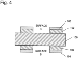
- Japanese Patent Application Laid-Open Publication No. 1993-259632 discloses a printed wiring board shown in Fig. 4 .
- an object of the art is to improve reliability of joint in a joint process.
- a conductor 102 which forms a wiring pattern made of a copper foil and which is used for soldering electric components to be mounted, is arranged on both surfaces (surface A and surface B) of a substrate 100.
- a solder layer (first solder layer) 105 which includes lead and an intermetallic compound of tin, is arranged on the conductor 102 of the surface A (one surface).
- a solder layer (second solder layer) 104 which is tin-lead based solder layer (tin-lead 63/37), is arranged on the conductor 102 of the surface B (the other surface).
- a melting point (227 degrees centigrade) of the solder layer 105 on the surface A is higher than a melting point (183 degrees centigrade) of the solder layer 104 on the surface B.
- the solder layers are formed on the conductors formed on both surfaces of the substrate 102, and the solder layer formed on the one surface is changed to an alloy of lead and an intermetallic compound of tin by carrying out the heating process. Since the melting point of the solder layer formed on the one surface is higher than the melting point of the solder layer formed on the other surface by virtue of the above mention, it is possible to prevent that a joint portion of an electric component, which has been mounted on the surface A set downward, is melted when melting the solder layer 104 on the surface B.
- JP 2013 016726 A discloses a solar cell panel having solar cells arranged on its surface.
- the solar cell panel comprises: a conductive bus bar connected to an end of a solar cell sequence in which a plurality of solar cells is serially connected and a conductor wire which is electrically connected to the bus bar in order to enable the flow of current obtained by the solar cells.
- the conductor wire has a first covering which has insulation properties and covers the conductor wire, and a second covering which has electrical conductivity and covers the first covering.
- US 2014/060611 A1 relates to a method for connecting solder-coated connection leads to photovoltaic solar cells.
- the solder-coated connection leads are made of aluminium or an aluminium alloy and the photovoltaic solar cells have metallizations on the upper side and the lower side.
- the soldering method for joining the parts can be IR soldering, inductive soldering, thermal contact soldering, ultrasonic soldering or hot air soldering.
- suitable solder materials consisting of different combinations of materials, e.g. tin, lead or copper.
- JP 2001 345467 A reveals an electrode structure of a photovoltaic element comprising current collecting electrodes of metal wire and bus bars touching the current collecting electrodes.
- the bus bar is attached to a part of the photovoltaic element through an adhesive and at least a part of the current collecting electrode has a bonding part sandwiched between the bus bar and the adhesive.
- the metal wire consists of a material with a low electric resistance.
- the material of the bus bar electrode can be a metal, such as Cu, Ag, Pt or the like or an alloy thereof. It can be shaped as a sheet, a tape, a foil or the like.
- the structure according to Japanese Patent Application Laid-Open Publication No. 1993-259632 increases the joint strength by making the melting temperature of the tin-based intermetallic compound, which is typically formed when phase transition of the lead solder takes place, different from the melting temperature of the alloy.
- the intermetallic compound is generally brittle as mentioned above, it is important to have the sufficient joint strength at the time of joint, and furthermore it is also necessary to avoid that the joint strength is degraded at the time of using an electronic device including the solder joint.
- the joint portion receives an impact of the heat cycle or the like, and consequently it is progressed that the joint portion deteriorates into the intermetallic compound and the metallic crystalline grains of the solder become coarse.
- a main object of the present invention is to provide lead solder joint structure and a manufacturing method thereof which can restrain degradation of the joint strength even if the high temperature or the heat cycle is applied.
- a method for manufacturing a lead soldered joint structure according to claim 4 is provided.
- the lead solder joint structure and the manufacturing method thereof which can restrain degradation of the joint strength even if the high temperature or the heat cycle is applied.
- Fig. 1 is a top view of a joint portion for explaining a lead solder joint structure according to the present exemplary embodiment
- Fig. 2 is a cross section view taken along A - A of Fig. 1 .
- Sn10 Sn: 10%, Ag: 2%, Pb: 88% ; solidus line: 267.8 degrees centigrade, liquidus line: 298.9 degrees centigrade
- lead solder Sn10
- FIG. 1 exemplifies lead solder joint structure 20 in which a wire (first member) 10 is joined to a conductor (second member) 11 by use of the Sn10 solder.
- a bus bar which is manufactured by use of a sheet of silver or a sheet of kovar plated with silver, is exemplified.
- the wire 10 a wiring member which is copper wire plated with silver is exemplified.
- the lead solder joint structure 20 includes a first solder layer 21 that is formed so as to include the wire 10 as a core, a second solder layer 22 which covers the first solder layer 21 and adheres to the conductor 11 through a third solder layer 24, and the third solder layer that exists between the second solder layer 22 and a solder joint surface side of the second member 11.
- the first solder layer 21 is a solder layer whose main constituent is a tin-copper based intermetallic compound.
- the second solder layer 22 is a solder layer whose main constituent is a lead-based alloy (that is, a solder layer which has a quite small amount of tin, and tin-based intermetallic compound).
- the third solder layer 24 is a solder layer whose main constituent is a tin-silver based intermetallic compound.
- the intermetallic compound is hard and brittle. Accordingly, the tin-copper based intermetallic compound and the tin-silver based intermetallic compound also have the same characteristics. Therefore, when the wire 10 or the conductor 11 is under stress caused by difference in expansion rate associating with heat cycles and the like, brittle fracture and the like may occur at the joint portion. Accordingly, there is a fear that reliability of joint is degraded.
- the intermetallic compound is gradually formed and the crystalline grains of the solder become coarse when an exposure time to a high temperature state becomes increasing not only continuously but also discontinuously during the course of usage even if a small amount of the intermetallic compound exists at the time of joint.
- the intermetallic compound is gradually formed at the joint portion soldered using the lead solder, and it is progressed that the crystalline grains of the solder become coarse in the forming process. As a result, the reliability of joint is degraded.
- the intermetallic compound is formed as much as possible after the joint portion is formed and before being put into use (before shipping of product) to consume tin completely.
- the intermetallic compound is formed as much as possible after the joint portion is formed and before being put into use (before shipping of product) to consume tin completely.
- the layer which is rich in tin becomes the first solder layer 21 and the third solder layer 24 which are corresponding to the layer including the intermetallic compound. Then, the layer which is poor in tin becomes the second solder layer 22 which is rich in lead.
- a main constituent of the second solder layer 22, which is rich in lead is an alloy of lead, and the second solder layer 22 is softer than the intermetallic compound (Young's modulus is low).
- the lead solder joint structure 20 is formed from the first solder layer 21 whose main constituent is the intermetallic compound covering the wire 10, the second solder layer 22 whose main constituent is the alloy of lead covering the first solder layer 21, and the third solder layer 24 which exists between the second solder layer 22 and the second member 11 and whose main constituent is the intermetallic compound.
- the wire 10 is arranged on the conductor 11.
- the wire 10 is soldered to the conductor 11 by using Sn10.
- the solder layer just after completion of soldering is denoted by reference numeral 23 in Fig. 3B .
- the solder layer is referred to as a simple joint layer 12, and a process for forming the simple joint layer is referred to as a simple joint layer forming process.
- the heat process (step of heat process) is carried out on the simple joint layer 12.
- a condition of the heat process a condition that a temperature of the heat process is 200 to 250 degrees centigrade and a time of the heat process is 1500 to 2000 hours is exemplified.
- the tin-based intermetallic compound is formed from tin which is included by the simple joint layer 12.
- Fig. 3C is a diagram exemplifying a state just after the completion of the heat process. Specifically, Fig 3C shows the first solder layer 21 and the third solder layer 24 which are rich in the intermetallic compound, and the second solder layer 22 whose tin is used for forming the first solder layer 21 and the third solder layer 24 and which consequently becomes poor in tin (rich in lead).
- the first solder layer 21 is the tin-copper based intermetallic compound which is formed by the solder layer 23 and the wire 10 reacting on each other in the heat process.
- the third solder layer 24 is the tin-silver based intermetallic compound which is formed by the solder layer 23 and the conductor 11 reacting on each other in the heat process.
- the intermetallic compound which is a brittle member, is formed in advance.
- various crystalline grains (intermetallic compound and ⁇ solid solution including a large amount of lead), which become coarse so that degradation in strength of the solder may be caused at the time of using the electronic device, are not formed.
- kirkendallvoid which is caused at a time of forming the intermetallic compound, by the heat process carried out for a long time.
- kirkendallvoid is one of factors which cause a crack in the solder joint, but by carrying out the heat process according to the present exemplary embodiment, it becomes difficult that new kirkendallvoid is formed at a time of using the electronic device.
- the solder layer 23 is changed to the second solder layer 22 which is poor in tin (rich in lead). Since the second solder layer 22 which is rich in lead is soft, even if the wire 10 is under heat stress, the second solder layer 22 can absorb the heat stress. Accordingly, it is possible to suppress a decrease in reliability of joint.
- the lead solder joint structure may be used to join such a waveguide and a waveguide flange.
- a base tube and a flange of the waveguide are brazed by the dip-brazing method, and afterward the brazed portion is plated with silver.
- the joint structure according to the exemplary embodiment for connecting the solar cell panels in series and in parallel.
- an interconnector which is made of silver or kovar plated with silver, is joined between cell electrodes by welding.
- a series of cells which are connected by the interconnectors is called a string.
- Sn62 Sn: 62%, Pb: 36%, Ag: 2%; melting point: 183 degrees centigrade
Claims (5)
- Bleilötverbindungsstruktur (20) mit einem ersten Element (10), das mit einem zweiten Element (11) mittels eines Bleilötmittels verbunden ist, wobei die Struktur aufweist:das erste Element (10);das zweite Element (11);eine erste Lötmittelschicht (21), die das erste Element (10) als einen Kern enthält und als Hauptbestandteil eine intermetallische Verbindung auf Zinn-Kupfer-Basis aufweist;eine zweite Lötmittelschicht (22), die zwischen der ersten Lötmittelschicht (21) und dem zweiten Element (11) vorhanden ist und die erste Lötmittelschicht (21) und das zweite Element (11) miteinander verbindet und Blei als einen Hauptbestandteil enthält; undeine dritte Lötmittelschicht (24), die zwischen der zweiten Lötmittelschicht (22) und dem zweiten Element (11) vorhanden ist und als einen Hauptbestandteil eine intermetallische Verbindung auf Zinn-Silber-Basis aufweist.
- Bleilötverbindungsstruktur (20) nach Anspruch 1,
wobei das Elastizitätsmodul der zweiten Lötmittelschicht (22) kleiner ist als das Elastizitätsmodul der ersten Lötmittelschicht (21) und der dritten Lötmittelschicht (24). - Bleilötverbindungsstruktur (20) nach Anspruch 1 oder 2,
wobei das erste Element (10) Kupferdraht ist und die Oberfläche des zweiten Elements (11) aus Silber besteht. - Verfahren zum Herstellen einer Bleilötverbindungsstruktur (20), in welchem ein erstes Element (10) unter Verwendung eines Bleilötmittels mit einem zweiten Element (11) verbunden wird, wobei das Verfahren aufweist:einen Lötprozess zum Ausbilden einer Verbindungsschicht (12, 23) durch Verbinden des ersten Elements (10) und des zweiten Elements (11) miteinander unter Verwendung des Bleilötmittels; undeinen Erwärmungsprozess zum Erwärmen eines Verbindungsabschnitts, der die Verbindungsschicht (12, 23) enthält, unter einer vorgegebenen Bedingung und zum Ändern der Verbindungsschicht (12, 23) in eine erste Lötmittelschicht (21), eine zweite Lötmittelschicht (22) und eine dritte Lötmittelschicht (24), wobei die erste Lötmittelschicht (21) das erste Element (10) als einen Kern enthält und als einen Hauptbestandteil davon eine intermetallische Verbindung auf Zinn-KupferBasis aufweist, wobei die zweite Lötmittelschicht (22), die zwischen der ersten Lötmittelschicht (21) und dem zweiten Element (11) vorhanden ist, die erste Lötmittelschicht (21) und das zweite Element (11) miteinander verbindet und als einen Hauptbestandteil Blei aufweist, und die dritte Lötmittelschicht (24), die zwischen dem zweiten Element (11) und der zweiten Lötmittelschicht (22) vorhanden ist als einen Hauptbestandteil eine intermetallische Verbindung auf Zinn-Silber-Basis aufweist,wobei das Bleilötmittel Sn10 ist,wobei die Erwärmungsprozessbedingung des Erwärmungsprozesses ist, dass eine Temperatur des Erwärmungsprozesses 200 bis 250 Grad Celsius beträgt und eine Zeit des Erwärmungsprozesses 1500 bis 2000 Stunden beträgt.
- Verfahren zum Herstellen der Bleilötverbindungsstruktur (20) nach Anspruch 4,
wobei das erste Element (10) Kupferdraht ist und die Oberfläche des zweiten Elements (11) aus Silber besteht.
Applications Claiming Priority (2)
| Application Number | Priority Date | Filing Date | Title |
|---|---|---|---|
| JP2015179112 | 2015-09-11 | ||
| JP2016154442A JP6329212B2 (ja) | 2015-09-11 | 2016-08-05 | 鉛半田接合構造及び製造方法 |
Publications (2)
| Publication Number | Publication Date |
|---|---|
| EP3167992A1 EP3167992A1 (de) | 2017-05-17 |
| EP3167992B1 true EP3167992B1 (de) | 2023-11-01 |
Family
ID=58317056
Family Applications (1)
| Application Number | Title | Priority Date | Filing Date |
|---|---|---|---|
| EP16187779.0A Active EP3167992B1 (de) | 2015-09-11 | 2016-09-08 | Bleilötverbindungsstruktur und verfahren zu ihrer herstellung |
Country Status (2)
| Country | Link |
|---|---|
| EP (1) | EP3167992B1 (de) |
| JP (1) | JP6329212B2 (de) |
Families Citing this family (1)
| Publication number | Priority date | Publication date | Assignee | Title |
|---|---|---|---|---|
| JP7182170B2 (ja) | 2019-03-04 | 2022-12-02 | 富士電機株式会社 | ジャーク測定システム |
Family Cites Families (10)
| Publication number | Priority date | Publication date | Assignee | Title |
|---|---|---|---|---|
| JPS5782065U (de) * | 1980-11-07 | 1982-05-20 | ||
| JPS60194062A (ja) * | 1984-03-14 | 1985-10-02 | Nippon Mining Co Ltd | 銅及び銅合金の表面処理方法 |
| JPS6286895A (ja) * | 1985-10-14 | 1987-04-21 | 株式会社日立製作所 | 電子部品のはんだ付け方法 |
| JPH05259632A (ja) | 1992-03-10 | 1993-10-08 | Matsushita Electric Ind Co Ltd | プリント配線板およびその製造方法 |
| JPH06296080A (ja) * | 1993-04-08 | 1994-10-21 | Sony Corp | 電子部品実装基板及び電子部品実装方法 |
| US5803344A (en) * | 1996-09-09 | 1998-09-08 | Delco Electronics Corp. | Dual-solder process for enhancing reliability of thick-film hybrid circuits |
| JP2001345467A (ja) * | 2000-06-01 | 2001-12-14 | Canon Inc | 光起電力素子の電極構造および製造方法 |
| JP5231727B2 (ja) * | 2006-09-29 | 2013-07-10 | 株式会社東芝 | 接合方法 |
| DE102011013928A1 (de) * | 2011-03-14 | 2012-09-20 | Schott Solar Ag | Verfahren zum Löten von Solarzellen |
| JP5659970B2 (ja) * | 2011-07-06 | 2015-01-28 | 三菱電機株式会社 | 太陽電池パネル |
-
2016
- 2016-08-05 JP JP2016154442A patent/JP6329212B2/ja active Active
- 2016-09-08 EP EP16187779.0A patent/EP3167992B1/de active Active
Also Published As
| Publication number | Publication date |
|---|---|
| JP6329212B2 (ja) | 2018-05-23 |
| JP2017054804A (ja) | 2017-03-16 |
| EP3167992A1 (de) | 2017-05-17 |
Similar Documents
| Publication | Publication Date | Title |
|---|---|---|
| KR101087202B1 (ko) | 태양 전지 모듈 | |
| JP4993916B2 (ja) | Inハンダ被覆銅箔リボン導線及びその接続方法 | |
| JP2004247402A (ja) | 太陽電池モジュールおよびその製造方法 | |
| KR101609036B1 (ko) | 태양 전지용 인터커넥터 및 태양 전지 모듈 | |
| US20090260689A1 (en) | Solar cell lead wire, method of making the same, and solar cell | |
| JP5702937B2 (ja) | 半導体装置 | |
| JP2008140787A (ja) | 太陽電池用はんだめっき線およびその製造方法 | |
| EP1484801A2 (de) | Solarzellenmodul und sein Herstellungsverfahren | |
| US9877399B2 (en) | Lead solder joint structure and manufacturing method thereof | |
| EP3167992B1 (de) | Bleilötverbindungsstruktur und verfahren zu ihrer herstellung | |
| JP4984431B2 (ja) | 集積型薄膜太陽電池、及びその製造方法 | |
| WO2020233839A1 (en) | Solder paste for module fabrication of solar cells | |
| JP2008294390A (ja) | モジュール構成 | |
| CN217799731U (zh) | 焊带用焊片、组合式焊带及组合式焊带串 | |
| JP2008098315A (ja) | 太陽電池用はんだめっき線およびその製造方法 | |
| JP5418189B2 (ja) | 太陽電池用リード線及びそれを用いた太陽電池 | |
| US20220069141A1 (en) | Low temperature metallic interconnect for solar cell shingling | |
| JP6586352B2 (ja) | 半導体装置の製造方法 | |
| WO2021241635A1 (ja) | 熱電変換モジュール及びその製造方法 | |
| CN205079882U (zh) | 带引线的热敏电阻组件 | |
| JP2014042065A (ja) | 太陽電池用リード線及び太陽電池 | |
| JP2005191201A (ja) | 太陽電池素子接続用インナーリード及び太陽電池モジュール並びに太陽電池モジュールの製造方法 | |
| JP3552704B2 (ja) | 熱電変換モジュール | |
| CN103943703A (zh) | 一种太阳电池用互连条及对应的太阳电池组件 | |
| JP2013152979A (ja) | 太陽電池モジュール及びその製造方法 |
Legal Events
| Date | Code | Title | Description |
|---|---|---|---|
| PUAI | Public reference made under article 153(3) epc to a published international application that has entered the european phase |
Free format text: ORIGINAL CODE: 0009012 |
|
| STAA | Information on the status of an ep patent application or granted ep patent |
Free format text: STATUS: THE APPLICATION HAS BEEN PUBLISHED |
|
| AK | Designated contracting states |
Kind code of ref document: A1 Designated state(s): AL AT BE BG CH CY CZ DE DK EE ES FI FR GB GR HR HU IE IS IT LI LT LU LV MC MK MT NL NO PL PT RO RS SE SI SK SM TR |
|
| AX | Request for extension of the european patent |
Extension state: BA ME |
|
| STAA | Information on the status of an ep patent application or granted ep patent |
Free format text: STATUS: REQUEST FOR EXAMINATION WAS MADE |
|
| 17P | Request for examination filed |
Effective date: 20171113 |
|
| RBV | Designated contracting states (corrected) |
Designated state(s): AL AT BE BG CH CY CZ DE DK EE ES FI FR GB GR HR HU IE IS IT LI LT LU LV MC MK MT NL NO PL PT RO RS SE SI SK SM TR |
|
| STAA | Information on the status of an ep patent application or granted ep patent |
Free format text: STATUS: EXAMINATION IS IN PROGRESS |
|
| 17Q | First examination report despatched |
Effective date: 20210715 |
|
| STAA | Information on the status of an ep patent application or granted ep patent |
Free format text: STATUS: EXAMINATION IS IN PROGRESS |
|
| GRAP | Despatch of communication of intention to grant a patent |
Free format text: ORIGINAL CODE: EPIDOSNIGR1 |
|
| STAA | Information on the status of an ep patent application or granted ep patent |
Free format text: STATUS: GRANT OF PATENT IS INTENDED |
|
| RIC1 | Information provided on ipc code assigned before grant |
Ipc: B23K 101/38 20060101ALN20230525BHEP Ipc: H05K 3/34 20060101ALI20230525BHEP Ipc: B23K 20/02 20060101ALI20230525BHEP Ipc: B23K 35/26 20060101ALI20230525BHEP Ipc: B23K 1/00 20060101AFI20230525BHEP |
|
| INTG | Intention to grant announced |
Effective date: 20230615 |
|
| GRAS | Grant fee paid |
Free format text: ORIGINAL CODE: EPIDOSNIGR3 |
|
| GRAA | (expected) grant |
Free format text: ORIGINAL CODE: 0009210 |
|
| STAA | Information on the status of an ep patent application or granted ep patent |
Free format text: STATUS: THE PATENT HAS BEEN GRANTED |
|
| AK | Designated contracting states |
Kind code of ref document: B1 Designated state(s): AL AT BE BG CH CY CZ DE DK EE ES FI FR GB GR HR HU IE IS IT LI LT LU LV MC MK MT NL NO PL PT RO RS SE SI SK SM TR |
|
| REG | Reference to a national code |
Ref country code: GB Ref legal event code: FG4D |
|
| REG | Reference to a national code |
Ref country code: CH Ref legal event code: EP |
|
| REG | Reference to a national code |
Ref country code: IE Ref legal event code: FG4D |
|
| REG | Reference to a national code |
Ref country code: DE Ref legal event code: R096 Ref document number: 602016083785 Country of ref document: DE |
|
| REG | Reference to a national code |
Ref country code: LT Ref legal event code: MG9D |
|
| REG | Reference to a national code |
Ref country code: NL Ref legal event code: MP Effective date: 20231101 |
|
| PG25 | Lapsed in a contracting state [announced via postgrant information from national office to epo] |
Ref country code: GR Free format text: LAPSE BECAUSE OF FAILURE TO SUBMIT A TRANSLATION OF THE DESCRIPTION OR TO PAY THE FEE WITHIN THE PRESCRIBED TIME-LIMIT Effective date: 20240202 |
|
| PG25 | Lapsed in a contracting state [announced via postgrant information from national office to epo] |
Ref country code: IS Free format text: LAPSE BECAUSE OF FAILURE TO SUBMIT A TRANSLATION OF THE DESCRIPTION OR TO PAY THE FEE WITHIN THE PRESCRIBED TIME-LIMIT Effective date: 20240301 |
|
| PG25 | Lapsed in a contracting state [announced via postgrant information from national office to epo] |
Ref country code: LT Free format text: LAPSE BECAUSE OF FAILURE TO SUBMIT A TRANSLATION OF THE DESCRIPTION OR TO PAY THE FEE WITHIN THE PRESCRIBED TIME-LIMIT Effective date: 20231101 |
|
| REG | Reference to a national code |
Ref country code: AT Ref legal event code: MK05 Ref document number: 1626650 Country of ref document: AT Kind code of ref document: T Effective date: 20231101 |
|
| PG25 | Lapsed in a contracting state [announced via postgrant information from national office to epo] |
Ref country code: NL Free format text: LAPSE BECAUSE OF FAILURE TO SUBMIT A TRANSLATION OF THE DESCRIPTION OR TO PAY THE FEE WITHIN THE PRESCRIBED TIME-LIMIT Effective date: 20231101 |
|
| PG25 | Lapsed in a contracting state [announced via postgrant information from national office to epo] |
Ref country code: AT Free format text: LAPSE BECAUSE OF FAILURE TO SUBMIT A TRANSLATION OF THE DESCRIPTION OR TO PAY THE FEE WITHIN THE PRESCRIBED TIME-LIMIT Effective date: 20231101 |
|
| PG25 | Lapsed in a contracting state [announced via postgrant information from national office to epo] |
Ref country code: ES Free format text: LAPSE BECAUSE OF FAILURE TO SUBMIT A TRANSLATION OF THE DESCRIPTION OR TO PAY THE FEE WITHIN THE PRESCRIBED TIME-LIMIT Effective date: 20231101 |
|
| PG25 | Lapsed in a contracting state [announced via postgrant information from national office to epo] |
Ref country code: NL Free format text: LAPSE BECAUSE OF FAILURE TO SUBMIT A TRANSLATION OF THE DESCRIPTION OR TO PAY THE FEE WITHIN THE PRESCRIBED TIME-LIMIT Effective date: 20231101 Ref country code: LT Free format text: LAPSE BECAUSE OF FAILURE TO SUBMIT A TRANSLATION OF THE DESCRIPTION OR TO PAY THE FEE WITHIN THE PRESCRIBED TIME-LIMIT Effective date: 20231101 Ref country code: IS Free format text: LAPSE BECAUSE OF FAILURE TO SUBMIT A TRANSLATION OF THE DESCRIPTION OR TO PAY THE FEE WITHIN THE PRESCRIBED TIME-LIMIT Effective date: 20240301 Ref country code: GR Free format text: LAPSE BECAUSE OF FAILURE TO SUBMIT A TRANSLATION OF THE DESCRIPTION OR TO PAY THE FEE WITHIN THE PRESCRIBED TIME-LIMIT Effective date: 20240202 Ref country code: ES Free format text: LAPSE BECAUSE OF FAILURE TO SUBMIT A TRANSLATION OF THE DESCRIPTION OR TO PAY THE FEE WITHIN THE PRESCRIBED TIME-LIMIT Effective date: 20231101 Ref country code: BG Free format text: LAPSE BECAUSE OF FAILURE TO SUBMIT A TRANSLATION OF THE DESCRIPTION OR TO PAY THE FEE WITHIN THE PRESCRIBED TIME-LIMIT Effective date: 20240201 Ref country code: AT Free format text: LAPSE BECAUSE OF FAILURE TO SUBMIT A TRANSLATION OF THE DESCRIPTION OR TO PAY THE FEE WITHIN THE PRESCRIBED TIME-LIMIT Effective date: 20231101 Ref country code: PT Free format text: LAPSE BECAUSE OF FAILURE TO SUBMIT A TRANSLATION OF THE DESCRIPTION OR TO PAY THE FEE WITHIN THE PRESCRIBED TIME-LIMIT Effective date: 20240301 |