EP3166136A1 - Structures à semi-conducteurs et leurs procédé de fabrication - Google Patents
Structures à semi-conducteurs et leurs procédé de fabrication Download PDFInfo
- Publication number
- EP3166136A1 EP3166136A1 EP16196137.0A EP16196137A EP3166136A1 EP 3166136 A1 EP3166136 A1 EP 3166136A1 EP 16196137 A EP16196137 A EP 16196137A EP 3166136 A1 EP3166136 A1 EP 3166136A1
- Authority
- EP
- European Patent Office
- Prior art keywords
- layer
- dummy gate
- region
- gate
- opening
- Prior art date
- Legal status (The legal status is an assumption and is not a legal conclusion. Google has not performed a legal analysis and makes no representation as to the accuracy of the status listed.)
- Withdrawn
Links
Images





Classifications
-
- H—ELECTRICITY
- H10—SEMICONDUCTOR DEVICES; ELECTRIC SOLID-STATE DEVICES NOT OTHERWISE PROVIDED FOR
- H10D—INORGANIC ELECTRIC SEMICONDUCTOR DEVICES
- H10D30/00—Field-effect transistors [FET]
- H10D30/60—Insulated-gate field-effect transistors [IGFET]
- H10D30/62—Fin field-effect transistors [FinFET]
- H10D30/6215—Fin field-effect transistors [FinFET] having multiple independently-addressable gate electrodes
-
- H—ELECTRICITY
- H10—SEMICONDUCTOR DEVICES; ELECTRIC SOLID-STATE DEVICES NOT OTHERWISE PROVIDED FOR
- H10D—INORGANIC ELECTRIC SEMICONDUCTOR DEVICES
- H10D30/00—Field-effect transistors [FET]
- H10D30/01—Manufacture or treatment
- H10D30/021—Manufacture or treatment of FETs having insulated gates [IGFET]
- H10D30/024—Manufacture or treatment of FETs having insulated gates [IGFET] of fin field-effect transistors [FinFET]
-
- H—ELECTRICITY
- H10—SEMICONDUCTOR DEVICES; ELECTRIC SOLID-STATE DEVICES NOT OTHERWISE PROVIDED FOR
- H10D—INORGANIC ELECTRIC SEMICONDUCTOR DEVICES
- H10D30/00—Field-effect transistors [FET]
- H10D30/60—Insulated-gate field-effect transistors [IGFET]
- H10D30/62—Fin field-effect transistors [FinFET]
-
- H—ELECTRICITY
- H10—SEMICONDUCTOR DEVICES; ELECTRIC SOLID-STATE DEVICES NOT OTHERWISE PROVIDED FOR
- H10D—INORGANIC ELECTRIC SEMICONDUCTOR DEVICES
- H10D30/00—Field-effect transistors [FET]
- H10D30/60—Insulated-gate field-effect transistors [IGFET]
- H10D30/62—Fin field-effect transistors [FinFET]
- H10D30/6211—Fin field-effect transistors [FinFET] having fin-shaped semiconductor bodies integral with the bulk semiconductor substrates
-
- H—ELECTRICITY
- H10—SEMICONDUCTOR DEVICES; ELECTRIC SOLID-STATE DEVICES NOT OTHERWISE PROVIDED FOR
- H10D—INORGANIC ELECTRIC SEMICONDUCTOR DEVICES
- H10D30/00—Field-effect transistors [FET]
- H10D30/60—Insulated-gate field-effect transistors [IGFET]
- H10D30/62—Fin field-effect transistors [FinFET]
- H10D30/6212—Fin field-effect transistors [FinFET] having fin-shaped semiconductor bodies having non-rectangular cross-sections
-
- H—ELECTRICITY
- H10—SEMICONDUCTOR DEVICES; ELECTRIC SOLID-STATE DEVICES NOT OTHERWISE PROVIDED FOR
- H10D—INORGANIC ELECTRIC SEMICONDUCTOR DEVICES
- H10D30/00—Field-effect transistors [FET]
- H10D30/60—Insulated-gate field-effect transistors [IGFET]
- H10D30/62—Fin field-effect transistors [FinFET]
- H10D30/6217—Fin field-effect transistors [FinFET] having non-uniform gate electrodes, e.g. gate conductors having varying doping
-
- H—ELECTRICITY
- H10—SEMICONDUCTOR DEVICES; ELECTRIC SOLID-STATE DEVICES NOT OTHERWISE PROVIDED FOR
- H10D—INORGANIC ELECTRIC SEMICONDUCTOR DEVICES
- H10D64/00—Electrodes of devices having potential barriers
- H10D64/01—Manufacture or treatment
- H10D64/017—Manufacture or treatment using dummy gates in processes wherein at least parts of the final gates are self-aligned to the dummy gates, i.e. replacement gate processes
-
- H—ELECTRICITY
- H10—SEMICONDUCTOR DEVICES; ELECTRIC SOLID-STATE DEVICES NOT OTHERWISE PROVIDED FOR
- H10D—INORGANIC ELECTRIC SEMICONDUCTOR DEVICES
- H10D64/00—Electrodes of devices having potential barriers
- H10D64/01—Manufacture or treatment
- H10D64/021—Manufacture or treatment using multiple gate spacer layers, e.g. bilayered sidewall spacers
-
- H—ELECTRICITY
- H10—SEMICONDUCTOR DEVICES; ELECTRIC SOLID-STATE DEVICES NOT OTHERWISE PROVIDED FOR
- H10D—INORGANIC ELECTRIC SEMICONDUCTOR DEVICES
- H10D64/00—Electrodes of devices having potential barriers
- H10D64/20—Electrodes characterised by their shapes, relative sizes or dispositions
- H10D64/27—Electrodes not carrying the current to be rectified, amplified, oscillated or switched, e.g. gates
- H10D64/311—Gate electrodes for field-effect devices
- H10D64/411—Gate electrodes for field-effect devices for FETs
- H10D64/511—Gate electrodes for field-effect devices for FETs for IGFETs
- H10D64/512—Disposition of the gate electrodes, e.g. buried gates
-
- H—ELECTRICITY
- H10—SEMICONDUCTOR DEVICES; ELECTRIC SOLID-STATE DEVICES NOT OTHERWISE PROVIDED FOR
- H10D—INORGANIC ELECTRIC SEMICONDUCTOR DEVICES
- H10D84/00—Integrated devices formed in or on semiconductor substrates that comprise only semiconducting layers, e.g. on Si wafers or on GaAs-on-Si wafers
- H10D84/01—Manufacture or treatment
- H10D84/0123—Integrating together multiple components covered by H10D12/00 or H10D30/00, e.g. integrating multiple IGBTs
- H10D84/0126—Integrating together multiple components covered by H10D12/00 or H10D30/00, e.g. integrating multiple IGBTs the components including insulated gates, e.g. IGFETs
- H10D84/0144—Manufacturing their gate insulating layers
-
- H—ELECTRICITY
- H10—SEMICONDUCTOR DEVICES; ELECTRIC SOLID-STATE DEVICES NOT OTHERWISE PROVIDED FOR
- H10D—INORGANIC ELECTRIC SEMICONDUCTOR DEVICES
- H10D84/00—Integrated devices formed in or on semiconductor substrates that comprise only semiconducting layers, e.g. on Si wafers or on GaAs-on-Si wafers
- H10D84/01—Manufacture or treatment
- H10D84/0123—Integrating together multiple components covered by H10D12/00 or H10D30/00, e.g. integrating multiple IGBTs
- H10D84/0126—Integrating together multiple components covered by H10D12/00 or H10D30/00, e.g. integrating multiple IGBTs the components including insulated gates, e.g. IGFETs
- H10D84/0158—Integrating together multiple components covered by H10D12/00 or H10D30/00, e.g. integrating multiple IGBTs the components including insulated gates, e.g. IGFETs the components including FinFETs
-
- H—ELECTRICITY
- H10—SEMICONDUCTOR DEVICES; ELECTRIC SOLID-STATE DEVICES NOT OTHERWISE PROVIDED FOR
- H10D—INORGANIC ELECTRIC SEMICONDUCTOR DEVICES
- H10D84/00—Integrated devices formed in or on semiconductor substrates that comprise only semiconducting layers, e.g. on Si wafers or on GaAs-on-Si wafers
- H10D84/01—Manufacture or treatment
- H10D84/02—Manufacture or treatment characterised by using material-based technologies
- H10D84/03—Manufacture or treatment characterised by using material-based technologies using Group IV technology, e.g. silicon technology or silicon-carbide [SiC] technology
- H10D84/038—Manufacture or treatment characterised by using material-based technologies using Group IV technology, e.g. silicon technology or silicon-carbide [SiC] technology using silicon technology, e.g. SiGe
-
- H—ELECTRICITY
- H10—SEMICONDUCTOR DEVICES; ELECTRIC SOLID-STATE DEVICES NOT OTHERWISE PROVIDED FOR
- H10D—INORGANIC ELECTRIC SEMICONDUCTOR DEVICES
- H10D84/00—Integrated devices formed in or on semiconductor substrates that comprise only semiconducting layers, e.g. on Si wafers or on GaAs-on-Si wafers
- H10D84/80—Integrated devices formed in or on semiconductor substrates that comprise only semiconducting layers, e.g. on Si wafers or on GaAs-on-Si wafers characterised by the integration of at least one component covered by groups H10D12/00 or H10D30/00, e.g. integration of IGFETs
- H10D84/82—Integrated devices formed in or on semiconductor substrates that comprise only semiconducting layers, e.g. on Si wafers or on GaAs-on-Si wafers characterised by the integration of at least one component covered by groups H10D12/00 or H10D30/00, e.g. integration of IGFETs of only field-effect components
- H10D84/83—Integrated devices formed in or on semiconductor substrates that comprise only semiconducting layers, e.g. on Si wafers or on GaAs-on-Si wafers characterised by the integration of at least one component covered by groups H10D12/00 or H10D30/00, e.g. integration of IGFETs of only field-effect components of only insulated-gate FETs [IGFET]
- H10D84/834—Integrated devices formed in or on semiconductor substrates that comprise only semiconducting layers, e.g. on Si wafers or on GaAs-on-Si wafers characterised by the integration of at least one component covered by groups H10D12/00 or H10D30/00, e.g. integration of IGFETs of only field-effect components of only insulated-gate FETs [IGFET] comprising FinFETs
-
- H—ELECTRICITY
- H10—SEMICONDUCTOR DEVICES; ELECTRIC SOLID-STATE DEVICES NOT OTHERWISE PROVIDED FOR
- H10P—GENERIC PROCESSES OR APPARATUS FOR THE MANUFACTURE OR TREATMENT OF DEVICES COVERED BY CLASS H10
- H10P14/00—Formation of materials, e.g. in the shape of layers or pillars
- H10P14/20—Formation of materials, e.g. in the shape of layers or pillars of semiconductor materials
- H10P14/24—Formation of materials, e.g. in the shape of layers or pillars of semiconductor materials using chemical vapour deposition [CVD]
-
- H—ELECTRICITY
- H10—SEMICONDUCTOR DEVICES; ELECTRIC SOLID-STATE DEVICES NOT OTHERWISE PROVIDED FOR
- H10P—GENERIC PROCESSES OR APPARATUS FOR THE MANUFACTURE OR TREATMENT OF DEVICES COVERED BY CLASS H10
- H10P50/00—Etching of wafers, substrates or parts of devices
- H10P50/20—Dry etching; Plasma etching; Reactive-ion etching
- H10P50/24—Dry etching; Plasma etching; Reactive-ion etching of semiconductor materials
- H10P50/242—Dry etching; Plasma etching; Reactive-ion etching of semiconductor materials of Group IV materials
Definitions
- the present invention generally relates to the field of semiconductor fabrication technology and, more particularly, relates to semiconductor structures and fabrication methods thereof.
- MOSFET metal-oxide-semiconductor field-effect-transistors
- Fin-FETs fin field-effect-transistors
- gate electrode is able to control an ultra-thin structure (e.g., a fin structure) from the two side surfaces of the ultra-thin structure. Therefore, Fin-FETs demonstrate much better gate-to-channel controllability than planar MOSFETs. As such, Fin-FETs may be able to significantly suppress the short-channel effects.
- Fin-FETs may also demonstrate better compatibility with the existing fabrication technology for integrated circuits.
- Fin-FETs may be classified mainly into two categories based on their functions, namely, core devices and peripheral devices (e.g. input/output (I/O) devices).
- core devices may be further categorized into two types: core N-type metal-oxide-semiconductor (NMOS) devices and core P-type metal-oxide-semiconductor (PMOS) devices; and the peripheral devices may be further categorized into two types: peripheral NMOS devices and peripheral PMOS devices.
- NMOS core N-type metal-oxide-semiconductor
- PMOS P-type metal-oxide-semiconductor
- peripheral devices may be further categorized into two types: peripheral NMOS devices and peripheral PMOS devices.
- the operation power voltage of the peripheral devices is significantly larger than the operation power voltage of the core devices. Therefore, the thickness of the gate dielectric layers in peripheral devices is usually larger than the thickness of the gate dielectric layers in core devices. In order to prevent electrical breakdown and other issues, for a device with a high operation power voltage, the thickness of the gate dielectric layer in the device may need to be increased. The thickness of the dielectric layers in peripheral devices may also need to be increased.
- a first aspect of the present invention includes a method for fabricating a semiconductor structure.
- the method includes forming a plurality of fin structures on a substrate including a peripheral region and a core region. Fin structures formed in the peripheral region are first fin structures and fin structures formed in the core region are second fin structures.
- the method for fabricating the semiconductor structure also includes forming a first dummy gate structure, including a first dummy gate electrode layer and a first dummy oxide layer, on each first fin structure, and a second dummy gate structure, including a second dummy gate electrode layer and a second dummy oxide layer, on each second fin structure.
- the method further includes forming a dielectric layer on the substrate having a top surface of the leveled with the top surfaces of the first dummy gate structures and the second dummy gate structures.
- the method then includes forming a first opening to expose the first dummy oxide layer by removing the first dummy gate electrode layer and a second opening to expose the second dummy oxide layer by removing the second dummy gate electrode layer, and removing the first dummy gate oxide layer in the first opening to expose a portion of the first fin structure.
- the method includes forming a first gate oxide layer on the exposed portion of each first fin structure, removing each second dummy gate oxide layer in the second opening to expose a portion of the second fin structure, and forming a gate dielectric layer to cover each first gate oxide layer, sidewall surfaces of each first opening, and bottom and sidewall surfaces of each second opening.
- the method for fabricating the semiconductor structure further includes forming a metal layer to cover the gate dielectric layer and fill up the first openings and the second openings.
- the first gate oxide layer, the gate dielectric layer, and the metal layer formed in each first opening together form a first gate structure
- the gate dielectric layer and the metal layer formed in each second opening together form a second gate structure.
- the first gate oxide layer, the gate dielectric layer, and the metal layer may be formed in each first opening form a first gate structure.
- the gate dielectric layer and the metal layer may be formed in each second opening form a second gate structure.
- the first gate oxide layer may formed by an in-situ steam generation (ISSG) oxidation process.
- Process parameters used in the ISSG oxidation process may include: a process gas including O 2 and H 2 ; a flow rate of O 2 in a range of 1 sccm to 30 sccm; a flow rate of H 2 in a range of 1.5 sccm to 15 sccm; and a chamber temperature in a range of 700 °C to 1200 °C.
- the dielectric layer may be made of one of HfO 2 , HfSiO, HfSiON, HfTaO, HfTiO, HfZrO, ZrO 2 , and Al 2 O 3 .
- the core region and the peripheral region may be both P-type regions, or may be both N-type regions.
- a work function layer may be formed on the gate dielectric layer.
- the work function layer may be made of an N-type work function material.
- the work function layer may be made of a P-type work function material.
- the N-type work function layer may be made of one or more of TiAl, TaAlN, TiAIN, MoN, TaCN, and AlN.
- the P-type work function layer may be made of one or more of Ta, TiN, TaN, TaSiN, and TiSiN.
- the first dummy gate structure and the second dummy gate structure may be formed by a process including: forming a dummy gate oxide film to cover the first fin structures and the second fin structures; forming a dummy gate electrode film on the dummy gate oxide film; forming a first patterned layer on the dummy gate electrode film, wherein positions, shapes, and dimensions of the first patterned layer define positions, shapes, and dimensions for subsequently-formed dummy gate electrode layers; performing an etching process to etch the dummy gate electrode film and the dummy gate oxide film to form a first dummy gate structure on each first fin structure in the peripheral region and form a second dummy gate structure on each second fin structure in the core region, wherein the first dummy gate structure includes a first dummy gate oxide layer and a first dummy gate electrode layer, and the second dummy gate structure includes a second dummy gate oxide layer and a second dummy gate electrode layer; and removing the first patterned layer.
- the first dummy gate electrode layer and the second dummy gate electrode layer may be removed in a same etching process.
- the first dummy gate electrode layer and the second dummy gate electrode layer may removed by a dry etching process.
- the removing of the first dummy oxide layer in the first opening may include: forming a second patterned layer to cover the core region, wherein the second patterned layer exposes a top surface of the first dummy gate oxide layer; performing a dry etching process to remove the first dummy gate oxide layer using the second patterned layer as an etch mask until a portion of the first fin structure is exposed on a bottom surface of the corresponding first opening; and removing the second patterned layer.
- the removing of the second dummy gate oxide layer may include: forming a third patterned layer to cover the peripheral region, wherein the third patterned layer exposes a top surface of the second dummy gate oxide layer; performing a dry etching process to remove the second dummy gate oxide layer using the third patterned layer as an etch mask until a portion of the second fin structure is exposed on a bottom surface of the corresponding second opening; and removing the third patterned layer.
- the first gate structure and the second gate structure may be formed by a process including: forming the gate dielectric layer on the first gate oxide layer in each first opening, sidewall surfaces of each first opening, and bottom and sidewall surfaces of each second opening, wherein the gate dielectric layer also covers the top surface of the dielectric layer; forming a work function layer on the gate dielectric layer; forming a metal layer on the work function layer to fill up the first openings and the second openings, wherein a top surface of the metal layer is higher than the top surface of the dielectric layer; removing a portion of the metal layer formed above the dielectric layer to form a first gate electrode layer on the work function layer in each first opening in the peripheral region and a second gate electrode layer on the work function layer in each second opening in the core region; and removing a portion of the gate dielectric layer and the work function layer formed above the dielectric layer to form a first gate dielectric layer on each first gate oxide layer as well as sidewall surfaces of the corresponding first opening in the peripheral region, a first work function layer on each first
- an interface layer may be formed on the first gate oxide layer in each first opening, sidewall surfaces of each first opening, and bottom and sidewall surfaces of each second opening, wherein the interface layer also covers the top surface of the dielectric layer.
- a portion of the interface layer formed above the dielectric layer may also be removed to form a first interface layer on each first gate oxide layer as well as sidewall surfaces of the corresponding first opening in the peripheral region, and a second interface layer on bottom and sidewall surfaces of each second opening in the core region.
- the first dummy gate structure may be made of one of polycrystalline silicon, SiO x , SiN x , SiON, SiCN, SiCON, and amorphous silicon.
- the second dummy gate structure may be made of one of polycrystalline silicon, SiO x , SiN x , SiON, SiCN, SiCON, and amorphous silicon.
- the method may further include: forming a first peripheral-region sidewall spacer on each sidewall surface of the first dummy fin structure and a first core-region sidewall spacer on each sidewall surface of the second dummy fin structure; forming a peripheral-region stress layer in the first fin structure on each side of the first dummy gate structure and a core-region stress layer in the second fin structure on each side of the second dummy gate structure; forming a second peripheral-region sidewall spacer on a sidewall surface of each first peripheral-region sidewall spacer and a second core-region sidewall spacer on a sidewall surface of each first core-region sidewall spacer; and forming a peripheral-region source region and a peripheral-region drain region in the first fin structure and the peripheral-region stress layer on each side of the first dummy gate structure and a core-region source region and a core-region drain
- the peripheral-region stress layer may be made of silicon.
- the peripheral-region stress layer may be formed by an epitaxial chemical vapor deposition growth process.
- the core-region stress layer may be made of silicon.
- the core-region stress layer may be formed by an epitaxial chemical vapor deposition growth process.
- Process parameters used in the epitaxial chemical vapor deposition growth process may include: a process temperature in a range of 500 °C to 950 °C; a process time in a range of 1000 s to 11000 s; a chamber pressure in a range of 5 Torr to 1000 Torr; a pretreatment gas of H 2 ; and a reaction gas including one or more of HCl, SiH 2 Cl 2 , and SiH 4 .
- a second aspect of the present invention provides a semiconductor structure.
- the semiconductor structure includes a semiconductor base structure.
- the semiconductor base structure includes a plurality of fin structures formed on a substrate including a peripheral region and a core region. Fin structures formed in the peripheral region are first fin structures and fin structures formed in the core region are second fin structures.
- the semiconductor structure further includes a first gate structure formed on a portion of each first fin structure in the peripheral region, a second gate structure formed on a portion of each second fin structure in the core region, and a dielectric layer formed on the substrate having a top surface leveled with top surfaces of the first gate structures and the second gate structures.
- the first gate structure in the peripheral region includes a first gate oxide layer formed on the first fin structure, a gate dielectric layer formed on the first gate oxide layer and sidewall surfaces of the corresponding first opening, and a first gate electrode layer formed on the first gate dielectric layer
- the second gate structure in the core region includes a second gate dielectric layer formed on the second fin structure and sidewall surfaces of the corresponding second opening, and a second gate electrode layer formed on the second gate dielectric layer.
- the first gate oxide layer is formed in a first opening formed by removing a first dummy gate structure, including a first dummy gate electrode layer and a first dummy gate oxide layer, previously formed on the first fin structure.
- the second gate structure is formed in a second opening formed by removing a second dummy gate structure, including a second dummy gate electrode layer and a second dummy gate oxide layer, previously formed on the second fin structure. Moreover, the second dummy gate oxide layer is removed after forming the first gate oxide layer.
- the first gate structure may also include a first interface layer formed on the first gate oxide layer and sidewall surfaces of the corresponding first opening.
- the first gate dielectric layer may be formed on the first interface layer.
- the second gate structure may also include a second interface layer formed on the exposed portion of the second fin structure in the second opening and also on sidewall surfaces of the corresponding second opening.
- the second gate dielectric layer may be formed on the second interface layer.
- the first gate structure may also include a first work function layer formed between the first gate dielectric layer and the first gate electrode layer.
- the second gate structure may also include a second work function layer formed between the second gate dielectric layer and the second gate electrode layer.
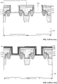
- Figures 1-5 show schematic cross-section views of semiconductor structures at certain stages of an existing fabrication process.
- the semiconductor base structure includes a substrate 100 and a plurality of fin structures protruding from the substrate 100.
- the substrate 100 includes a peripheral region I and a core region II, and the plurality of fin structures are formed in both the peripheral region I and the core region II.
- the semiconductor base structure is described to have a first fin structure 110 formed on the substrate 100 in the peripheral region I and a second fin structure 120 formed on the substrate 100 in the core region II.
- the semiconductor base structure also includes a first dummy gate structure (not shown) formed in the peripheral region I, a second dummy gate structure (not shown) formed in the core region II, peripheral-region source/drain regions 113 formed on the two sides of the first dummy gate structure, core-region source/drain regions 123 formed on the two sides of the second dummy gate structure.
- the first dummy gate structure also includes a first dummy gate oxide layer 111 formed on the surface of the first fin structure 110, and a first dummy gate electrode layer 112 formed on the surface of the first dummy gate oxide layer 111.
- the second dummy gate structure also includes a second dummy gate oxide layer 121 formed on the surface of the second fin structure 120, and a second dummy gate electrode layer 122 formed on the surface of the second dummy gate oxide layer 121.
- the semiconductor base structure further includes a dielectric layer 130 covering the side surfaces of the first dummy gate structure and the second dummy gate structure.
- the first dummy gate electrode layer 112 (referring to Figure 1 ) is removed by etching to expose a portion of the surface of the first dummy gate oxide layer 111 and form a first opening 200 in the dielectric layer 130.
- the second dummy gate electrode layer 122 (referring to Figure 1 ) is also removed by etching to expose a portion of the surface of the second dummy gate oxide layer 121 and form a second opening 210 in the dielectric layer 130.
- a first patterned layer 300 is formed to cover the peripheral region I. Specifically, the first patterned layer 300 covers the dielectric layer 130 in the peripheral region I and also fills up the first opening 200 (referring to Figure 2 ). However, the first patterned layer 300 does not cover the second dummy gate oxide layer 121 (referring to Figure 2 ) on the bottom of the second opening 210. That is, the second dummy gate oxide layer 121 (referring to Figure 2 ) on the bottom of the second opening 210 is exposed. Further, the second dummy gate oxide layer 121 on the bottom of the second opening 210 is removed through an etching process using the first patterned layer 300 as an etch mask. Finally, the first patterned layer 300 is removed after removing the second dummy gate oxide layer 121.
- an interface layer 140 is formed on the surface of the first dummy gate oxide layer 111 situated on the bottom of the first opening 200 (referring to Figure 2 ), the sidewall surfaces of the first opening 200, the bottom surface of the second opening 210 (referring to Figure 2 ), and the sidewall surfaces of the second opening 210.
- the interface layer 140 also covers the surface of the dielectric layer 130.
- a gate dielectric layer 150 is formed on the surface of the interface layer 140, and then a work function layer 160 is formed on the surface of the gate dielectric layer 150.
- a metal layer (not shown) is formed on the work function layer 160.
- the metal layer fills up the first opening 200 (referring to Figure 2 ) and the second opening 210 (referring to Figure 2 ).
- the top surface of the metal layer is higher than the top surface of the dielectric layer 130.
- the portion of the metal layer formed above the top surface of the dielectric layer 130 is then removed by polishing.
- a first gate electrode layer 114 is formed on the surface of the work function layer 160 in the peripheral region I and a second gate electrode layer 124 is formed on the surface of the work function layer 160 in the core region II.
- a first interface layer 115 is formed on the surface of the first dummy gate oxide layer 111 and the sidewall surfaces of the first opening 200 (referring to Figure 2 ), a first gate dielectric layer 116 is formed on the surface of the first interface layer 115, and a first work function layer 117 is formed on the surface of the first gate dielectric layer 116.
- a second interface layer 125 is formed on the bottom and the sidewall surfaces of the second opening 210 (referring to Figure 2 ), a second gate dielectric layer 126 is formed on the surface of the second interface layer 125, and a second work function layer 127 is formed on the surface of the second gate dielectric layer 126.
- the first dummy gate oxide layer 111, the first interface layer 115, the first gate dielectric layer 116, the first work function layer 117, and the first gate electrode layer 114 together form a first gate structure in the peripheral region I.
- the second interface layer 125, the second gate dielectric layer 126, the second work function layer 127, and the second gate electrode layer 124 together form a second gate structure in the core region II.
- the first dummy gate oxide layer 111 is served as a part of the first gate structure.
- the etching process performed in the course of fabricating the first dummy gate structure may easily cause damages to the first dummy gate oxide layer 111, and thus may further affect the quality of the subsequently-formed first gate structure in the peripheral region I. Because the damaged region may be closed to the channel edge of the peripheral device, the electrical performance of the semiconductor device may be degraded.
- the present invention provides a semiconductor structure and a method for fabricating a semiconductor structure.
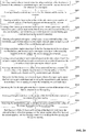
- Figure 20 shows a flowchart of an exemplary fabrication process consistent with the disclosed embodiments.
- Figures 6-19 show schematic views of semiconductor structure at certain stages of the fabrication process consistent with the disclosed embodiments.
- a semiconductor base structure is formed (S801).
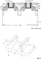
- Figure 6 shows a perspective view of the semiconductor base structure.
- Figure 7 shows a schematic cross-section view of the semiconductor base structure shown in Figure 6 along an AA1 line.
- a semiconductor base structure may be formed.
- the semiconductor base structure may include a substrate 400 and a plurality of fin structures protruding from the substrate 400.
- the substrate 400 may further include a peripheral region I (referring to Figure 7 ) and a core region II (referring to Figure 7 ).
- a plurality of fin structures may be formed on the substrate in both the peripheral region I and the core region II.
- the semiconductor base structure is described to have a first fin structure 410 formed on the substrate 400 in the peripheral region I and a second fin structure 420 formed on the substrate 400 in the core region II, although any number of fin structures may be formed in each of the peripheral region I and the core region II.
- a Fin-FET subsequently-formed in the peripheral region I may be used for signal I/O, and the operation power voltage of the Fin-FET subsequently-formed in the peripheral region I may be larger than the operation power voltage of a Fin-FET subsequently-formed in the core region II.
- the substrate 400 may be made of one of silicon, germanium, SiGe, SiC, GaAs, InAs, etc.
- the substrate 400 may also be a silicon on insulator (SOI) or germanium on insulator (GOI) substrate.
- the first fin structure 410 and the second fin structure 420 may be made of one of silicon, germanium, SiGe, SiC, GaAs, InAs, etc.
- the substrate 400 is a silicon substrate, and the first fin structure 410 and the second fin structure 420 are also made of silicon.
- the peripheral region I and the core region II may both be N-type regions or may both be P-type regions.
- the semiconductor base structure may be formed by a process including the following steps. First, an initial substrate is provided. A patterned layer (not shown) may be formed on the surface of the initial substrate. A hard mask layer 500 may be formed on the surfaces of the patterned layer and the initial substrate. Further, an etching process may be performed on the hard mask layer 500, which is formed on the top of the patterned layer and the initial substrate. After the etching process, only the portion of the hard mask layer 500 formed on the sidewall surfaces of the patterned layer may remain. The patterned layer may then be removed to expose a portion of the initial substrate. The shape, the dimension, and the position of the remaining patterned hard mask layer 500 may define the shape, the dimension, and the position of the fin structures to be formed.
- a plurality of discrete bulges may be formed by etching the initial substrate along the exposed surface of the initial substrate using the remaining patterned hard mask layer 500 as an etch mask.
- the bulges formed by the etching process may become the fin structures of the semiconductor base structure, and the etched initial substrate may become the substrate 400.
- the substrate 400 further includes a peripheral region I and a core region II.
- the fin structure formed in the peripheral region I may be the first fin structure 410 and the fin structure formed in the core region II may be the second fin structure 420, as shown in Figure 7 .
- the top dimension of the first fin structure 410 may be smaller than the bottom dimension of the first fin structure 410
- the top dimension of the second fin structure 420 may be smaller than the bottom dimension of the second fin structure 420.
- the sidewalls of the first fin structure may be perpendicular to the surface of the substrate. That is, the top dimension of the first fin structure may be equal to the bottom dimension of the first fin structure.
- the sidewalls of the second fin structure may be perpendicular to the surface of the substrate. That is, the top dimension of the second fin structure may be equal to the bottom dimension of the second fin structure.
- the portion of the hard mask layer 500 situated on the top of the first fin structure 410 and the second fin structure 420 may be kept.
- the hard mask layer 500 may be made of SiN x .
- the hard mask layer 500 may serve as a stop layer for the planarization process.
- the hard mask layer 500 may also provide protection for the top of the first fin structure 410 and the second fin structure 420 during subsequent fabrication processes.
- the semiconductor base structure may also be formed by a process including the following steps. First, an initial substrate is provided. A patterned hard mask layer may be formed on the surface of the initial substrate. The position, the shape, and the dimension of the patterned hard mask layer may define the position, the shape, and the dimension of the subsequently-formed fin structures. Then, a plurality of bulges may be formed by etching the initial substrate using the patterned mask layer as an etch mask. The bulges formed by the etching process may be the fin structures and the etched initial substrate may become the substrate.
- the substrate further includes a peripheral region and a core region. The fin structure formed in the peripheral region may be the first fin structure and the fin structure formed in the core region may be the second fin structure.
- a linearly-oxidized layer may be formed on the surface of the first fin structure and the second fin structure (S802).
- Figure 8 shows a schematic cross-section view of a corresponding semiconductor structure.
- a linearly-oxidized layer 401 may be formed on each of the first fin structure 410 and the second fin structure 420.
- the linearly-oxidized layer 401 may be used to recondition the first fin structure 410 and the second fin structure 420.
- first fin structure 410 and the second fin structure 420 are formed by etching the initial substrate, the first fin structure 410 and the second fin structure 420 may often have protruding edges and corners. In addition, defects may also exist at the surfaces of the first fin structure 410 and the second fin structure 420. Therefore, the performance of subsequently-formed Fin-FETs may be affected.
- an oxidation treatment process may be performed on the first fin structure 410 and the second fin structure 420 to form a linearly-oxidized layer 401 on each of the first fin structure 410 and the second fin structure 420.
- the protruding edges and corners of the first fin structure 410 and the second fin structure 420 may have a larger specific surface area than structures with flat surfaces, the protruding edges and corners may be easily oxidized during the oxidation treatment process. Therefore, after removing the linearly-oxidized layer 401 in a subsequent process, not only the defect layer at the surface of the first fin structure 410 and the second fin structure 420 may be removed, but the protruding edges and corners may be removed.
- the surfaces of the first fin structure 410 and the second fin structure 420 may become smooth and the lattice quality may also be improved.
- point discharge at the top tips of the first fin structure 410 and the second fin structure 420 may be avoided, which may further help improve the performance of the Fin-FETs.
- the oxidation treatment process may be an oxygen plasma oxidation process or a solution oxidation process using a mixture of sulfuric acid and hydrogen peroxide.
- the oxidation treatment process may also oxidize the surface of the substrate 400. Therefore, a linearly-oxidized layer 401 may also be formed at the surface of the substrate 400.
- the oxygen treatment process performed on the first fin structure 410 and the second fin structure 420 in order to form the linearly-oxidized layers 401 may be an in-situ steam generation (ISSG) oxidation process. Accordingly, the linearly-oxidized layers 401 are made of SiO 2 .
- an isolation layer may be formed on the surface of the substrate (S803).
- Figure 9 shows a schematic cross-second view of the semiconductor structure.
- an isolation layer 402 may be formed on the surface of the substrate 400.
- the isolation layer 402 may be used as an isolation structure in semiconductor structure. Specifically, the isolation layer 402 may be used to electrically isolate adjacent devices.
- the isolation layer 402 may be made of SiO x , SiN x , SiON, or any appropriate material. In one embodiment, the isolation layer 402 is made of SiO x .
- the isolation layer 402 is a shallow trench isolation (STI) layer.
- the isolation layer may not be limited to STI layer and may have other appropriate forms that may provide sufficient electrical isolation between neighboring devices.
- the isolation layer 402 may be formed by a process including the following steps. First, an isolation film may be formed on the surfaces of the linearly-oxidized layers 401. The isolation film may also cover the surface of the hard mask layer 500; that is, the top of the isolation film may be higher than the top of the hard mask layer 500. A planarization process may be performed on the isolation film until the surface of the hard mask layer 500 is exposed. Further, the isolation layer 402 may be formed by removing a top portion of the isolation film through an etch-back process. Finally, a portion of each linearly-oxidized layer 401 formed above the top surface of the isolation layer 402 (referring to Figure 8 ) may be removed, and then the hard mask layer 500 may also be removed.
- the material used to form the isolation film may be different from the materials used for the first fin structure 410, the second fin structure 420, and substrate 400.
- the isolation layer may be made of a material that can be easily removed. As such, during the subsequent process to remove the portion of the isolation film, damages to the first fin structure 410 and the second fin structure 420 may be avoided.
- the isolation film may be made of one of amorphous silicon, SiO x , SiON, SiC, SiOC, SiCON, etc.
- the isolation film may be formed by chemical vapor deposition (CVD), physical vapor deposition (PVD), or atomic layer deposition (ALD).
- CVD chemical vapor deposition
- PVD physical vapor deposition
- ALD atomic layer deposition
- the isolation film is made of SiO x and formed by a CVD process.
- a chemical mechanical planarization process may be performed to planarize the isolation film until the surface of the mask layer 500 is exposed. Then, the isolation layer 402 may be formed by performing a dry etching process, a wet etching process, or a process combining dry etching and wet etching to remove a portion of the isolation film.
- the ratio between the thickness of the isolation layer 402 and the height of the first fin structure 410 or the second fin structure 420 may be greater than or equal to 1 ⁇ 4 but less than or equal to 1 ⁇ 2. In one embodiment, the ratio between the thickness of the isolation layer 402 and the height of the first fin structure 410 or the second fin structure 420 is 1 ⁇ 2.
- a first dummy gate structure may be formed on the first fin structure and a second dummy gate structure may be formed on the second fin structure (S804).
- Figure 10 shows a schematic cross-section view of a corresponding semiconductor structure. Specifically, the schematic view shown in Figure 10 corresponds to the cross-section of the semiconductor structure along a BB1 line (referring to Figure 6 ).
- a first dummy gate structure (not shown) may be formed on the surface of the first fin structure 410 and a second dummy gate structure (not shown) may be formed on the surface of the second fin structure 420.
- the first dummy gate structure and the second dummy gate structure may be used to occupy spaces for a subsequently-formed first gate structure and a subsequently-formed second gate structure, respectively.
- the first dummy gate structure includes a first dummy gate oxide layer 411 and a first dummy gate electrode layer 412; the second dummy gate structure includes a second dummy gate oxide layer 421 and a second dummy gate electrode layer 422.
- the first dummy gate oxide layer 411 and the second dummy gate oxide layer 421 may be made of SiO x .
- the first dummy gate electrode layer 412 and the second dummy gate electrode layer 422 may be made of polycrystalline silicon, SiO x , SiN x , SiON, SiCN, SiCON, or amorphous silicon.
- the first dummy gate electrode layer 412 and the second dummy gate electrode layer 422 are both made of polycrystalline silicon.
- the first dummy gate structure and the second dummy gate structure may be formed by a process including the following steps.
- a dummy gate oxide film may be formed on the surfaces of the first fin structure 410 and the second fin structure 420.
- the dummy gate oxide film may also cover the surfaces of the substrate 400 and the isolation layer 402.
- a dummy gate electrode film may then be formed on the surface of the dummy gate oxide film, and a first patterned layer 510 may be formed on the surface of the dummy gate electrode film.
- the position, the shape, and the dimension of the first patterned layer 510 may define the position, the shape, and the dimension for subsequently-formed dummy gate electrode layers.
- An etching process may then be performed using the first patterned layer 510 as an etch mask to sequentially etch the dummy gate electrode film and the dummy gate oxide film.
- a first dummy gate structure may be formed on the surface of the first fin structure 410 in the peripheral region I and a second dummy gate structure may be formed on the surface of the second fin structure 420 in the core region II.
- the first dummy gate structure may include a first dummy gate oxide layer 411 and a first dummy gate electrode layer 412 while the second dummy gate structure may include a second dummy gate oxide layer 421 and a second dummy gate electrode layer 422.
- the first patterned layer 510 may be removed.
- the first patterned layer 510 is a hard mask layer.
- the first patterned layer 510 may be made of SiN x .
- a first peripheral-region sidewall spacer may be formed on each sidewall of the first dummy gate structure in the peripheral region and a first core-region sidewall spacer may also be formed on each sidewall of the second dummy gate structure in the core region (S805).
- Figure 11 shows a schematic cross-section view of the corresponding structure along the BB1 line (referring to Figure 6 ).
- a first peripheral-region sidewall spacer 413 may be formed on each sidewall surface of the first dummy gate structure in the peripheral region I and a first core-region sidewall spacer 423 may be formed on each sidewall surface of the second dummy gate structure in the core region II.
- the first peripheral-region sidewall spacer 413 formed in the peripheral region I may be made of SiO x , SiN x , SiC, SiCN, SiCON, SiON, BN, or BCN.
- the first peripheral-region sidewall spacer 413 formed in the peripheral region I may have a single-layer structure or a multiple-layer structure.
- the first core-region sidewall spacer 423 formed in the core region II may be made of SiO x , SiN x , SiC, SiCN, SiCON, SiON, BN, or BCN.
- the first core-region sidewall spacer 423 formed in the core region II may have a single-layer structure or a multiple-layer structure.
- the first peripheral-region sidewall 413 in the peripheral region I may have a single-layer structure and may be made of SiN x ; while the first core-region sidewall 423 in the core region II may have a single-layer structure and may be made of SiN x .
- the first peripheral-region sidewall spacer 413 in the peripheral region I and the first core-region sidewall spacer 423 in the core region II may be formed by a process including the following steps.
- a first sidewall film may be formed on the surfaces of the first dummy gate structure and the second dummy gate structure.
- the first sidewall film may also cover the surfaces of the substrate 400 and the isolation layer 402.
- the portion of the first sidewall film formed on the top surfaces of the first dummy gate electrode layer 412 and the second dummy gate electrode layer 422 may be removed by performing a maskless etching process.
- a first peripheral-region sidewall spacer 413 may be formed on each sidewall surface of the first dummy gate structure in the peripheral region I and a first core-region sidewall spacer 423 may be formed on each sidewall surface of the second dummy gate structure in the core region II.
- the maskless etching process may be a plasma dry etching process.
- the portion of the first sidewall film formed on the top of the first dummy gate electrode layer 412 and the top of the second dummy gate electrode layer 422 may be removed by etching to form a first peripheral-region sidewall spacer 413 on each sidewall of the first dummy gate structure in the peripheral region I and a first core-region sidewall spacer 423 on each side wall of the second dummy gate structure in the core region II.
- a portion of the first sidewall film formed on the surfaces of the substrate 400 and the isolation layer 402 may be removed.
- a peripheral-region stress layer may be formed in the first fin structure on the two sides of the first dummy gate structure, and a core-region stress layer may be formed in second fin structure on the two sides of the second dummy gate structure (S806).
- Figure 12 shows a schematic cross-section view of the semiconductor structures.
- a peripheral-region stress layer 414 may be formed in the first fin structure 410 on the two sides of the first dummy gate structure.
- a core-region stress layer 424 may be formed in the second fin structure 420 on the two sides of the second dummy gate structure.
- the peripheral-region stress layer 414 and the core-region stress layer 424 may be used to reduce the resistance of the device as well as the contact resistance in the device. In the meantime, the peripheral-region stress layer 414 and the core-region stress layer 424 may also induce appropriate stress into the channel region of devices in the peripheral region I and also into the channel region of devices in the core groin II. Therefore, the mobility of electrons and holes may be improved, and thus the performance of the semiconductor device may also be improved.
- the peripheral-region stress layer 414 and the core-region stress layer 424 may be formed by a process including the following steps.
- a mask layer (not shown) may be formed on the surface of the semiconductor base structure.
- the mask layer may also cover the surfaces of the first dummy gate structure, the second dummy gate structure, the isolation layer 402, and the substrate 400.
- the mask layer may expose a portion of the surface of the first fin structure 410 on each side of the first dummy gate structure and a portion of the surface of the second fin structure 420 on each side of the second dummy gate structure.
- the exposed portion of the first fin structure 410 and the second fin structure 420 may be etched by a first etching process using the mask layer as an etch mask.
- An initial opening may then be formed in the first fin structure 410 on each side of the first dummy gate structure; in addition, an initial opening (not shown) may also be formed in the second fin structure 420 on each side of the second dummy gate structure.
- Each initial openings may be further etched by a second etching process using the mask layer as an etch mask to form a trench (not shown).
- the depth of the trench may be larger than the depth of the initial opening, while the cross-sectional area of the trench may also be larger than the cross-sectional area of the initial opening.
- the mask layer may be removed by a wet etching process or by an ashing process.
- a peripheral-region stress layer 414 may be formed in each trench formed in the first fin structure 410 and a core-region stress layer 424 may be formed in each trench formed in the second fin structure 420.
- the first etching process is a plasma dry etching process.
- the process parameters used in the first etching process may include an etch gas including one or more of CF 4 , CH 3 F, HBr, NF 3 , Cl 2 , O 2 , and N 2 , a carrier gas including at least one of Ar and He, a chamber pressure in a range of 2 mTorr to 100 mTorr, an offset voltage in a range of 50 V to 250 V, a process temperature in a range of 30 °C to 100 °C, and a process time in a range of 3 s to 20 s.
- the second etching process is a wet etching process.
- the wet etching process may demonstrate a large etch selectivity ratio on silicon. Specifically, during the wet etching process, the etching rate on silicon is anisotropic, and thus trenches may then be formed in the first fin structure 410 on the two sides of the first dummy gate structure and in the second fin structure 420 on the two sides of the second dummy gate structure.
- the wet etching process may use an etching liquid including tetramethyl ammonium hydroxide solution.
- the process temperature may be in a range of 20 °C to 120 °C and the process time may be in a range of 20 s to 500 s.
- the peripheral-region stress layer 414 and the core-region stress layer 424 may be made of one of silicon, germanium, SiGe, SiC, GaAs, InAs, etc. In one embodiment, the peripheral-region stress layer 414 and the core-region stress layer 424 are both made of silicon.
- the peripheral-region stress layer 414 and the core-region stress layer 424 may be formed by an epitaxial CVD growth process.
- the lattice constant of the material used to form the peripheral-region stress layer 414 may be the same as the lattice constant of the material of the first fin structure 410, while the lattice constant of the material used to form the core-region stress layer 424 may be the same as the lattice constant of the material of the second fin structure 420.
- an epitaxial film may be grown layer by layer along the crystal orientation of the exposed surface of the first fin structure 410 in each trench of the peripheral region; in the meantime, an epitaxial film may also be grown layer by layer along the crystal orientation of the exposed surface of the second fin structure 420 in each trench of the core region.
- the epitaxial CVD growth process may be performed until a peripheral-region stress layer 414 with a thickness meeting a targeted value is formed in the first fin structure 410 while a core-region stress layer 424 with a thickness meeting a targeted value is formed in the second fin structure 420.
- the top surface of the formed peripheral-region stress layer 414 may be higher than the top surface of the first dummy gate oxide layer 411 while the top surface of the formed core-region stress layer 424 may be higher than the top surface of the second dummy gate oxide layer 421.
- the process parameters used in the epitaxial CVD growth process may include a process temperature in a range of 500 °C and 950 °C, a process time in a range of 1000 s to 11000 s, a chamber pressure in a range of 5 Torr to 1000 Torr.
- a pretreatment gas used in the epitaxial CVD growth process for forming the peripheral-region stress layer 414 and the core-region stress layer 424 may be hydrogen
- a reaction gas used in the epitaxial CVD growth process for forming the peripheral-region stress layer 414 and the core-region stress layer 424 may include one or more of HCl, SiH 2 Cl 2 , SiH 4 , etc.
- a second peripheral-region sidewall spacer may be formed on the side surface of each first peripheral-region sidewall spacer in the peripheral region and a second core-region sidewall spacer may be formed on the side surface of each first core-region sidewall spacer in the core region (S807).
- Figure 13 shows a schematic cross-section view of a corresponding semiconductor structure.
- a second peripheral-region sidewall spacer 415 may be formed on the side surface of each first peripheral-region sidewall spacer in the peripheral region I.
- a second core-region sidewall spacer 425 may be formed on the side surface of each first core-region sidewall spacer in the core region II.
- the second peripheral-region sidewall spacer 415 may be made of SiO x , SiN x , SiC, SiCN, SiCON, SiON, BN, or BCN.
- the second peripheral-region sidewall spacer 415 may have a single-layer structure or a multiple-layer structure.
- the second core-region sidewall spacer 425 may also be made of SiO x , SiN x , SiC, SiCN, SiCON, SiON, BN, or BCN.
- the second core-region sidewall spacer 425 may also have a single-layer structure or a multiple-layer structure.
- the second peripheral-region sidewall spacer 415 may have a single-layer structure and may be made of SiN x ; while , the second core-region sidewall spacer 425 may also have a single-layer structure and may be made of SiN x .
- the second peripheral-region sidewall spacer 415 and the core-region sidewall spacer 425 may be made of a process including the following steps.
- a second sidewall film may cover the top surfaces of the first dummy gate electrode layer 412 and the second dummy gate electrode layer 422 as well as the surface of the isolation layer 402.
- the portion of the second sidewall film formed on the top surfaces of the first dummy gate electrode layer 412 and the second dummy gate electrode layer 422 may be removed by performing a maskless etching process.
- a second peripheral-region sidewall spacer 415 may be formed on each sidewall surface of the first peripheral-region sidewall spacer 413 in the peripheral region I and a second core-region sidewall spacer 425 may be formed on each sidewall surface of the first core-region sidewall spacer 423 in the core region II.
- the maskless etching process may be a dry etching process.
- the portion of the second sidewall film formed on the top of first dummy gate electrode layer 412 and the top of the second dummy gate electrode layer 422 may be removed by etching to form a second peripheral-region sidewall spacer 415 on each sidewall of the first peripheral-region sidewall spacer 413 in the peripheral region I and a second core-region sidewall spacer 425 on each side wall of the first core-region sidewall spacer 423 in the core region II.
- a portion of the second sidewall film formed on the surface of the isolation layer 402 may be removed.
- a peripheral-region source/drain region may be formed in the first fin structure 410 and the peripheral-region stress layer 414 on each side of the first dummy gate structure.
- a core-region source/drain region may also be formed in the second fin structure 420 and the core-region stress layer 424 on each side of the second dummy gate structure.
- a dielectric layer may be formed on the surface of the semiconductor base structure (S808).
- Figure 14 shows a schematic cross-section view of a corresponding semiconductor structure.
- a dielectric layer 460 may be formed on the surface of the semiconductor base structure.
- the top surface of the dielectric layer 460 may be leveled with the top surfaces of the first dummy gate structure and the second dummy gate structure. That is, the top surfaces of the dielectric layer, the first dummy gate electrode layer 412, and the second dummy gate electrode layer 422 may be leveled with each other such that the first dummy gate electrode layer 412 and the second dummy gate electrode layer 422 may be exposed.
- the dielectric layer 460 may be situated on the surface of the isolation layer 402 as well as a portion of the surface of the first fin structure 410 and a portion of the surface of the second fin structure 420.
- the dielectric layer 470 may also cover the peripheral-region source/drain regions (not shown) and the core-region source/drain regions (not shown) in the II.
- the top surfaces of the dielectric layer, the first dummy gate electrode layer 412, and the second dummy gate electrode layer 422 may be leveled with each other.
- the dielectric layer 460 may have a multiple-layer structure. Specifically, the dielectric layer 460 may include a first dielectric layer 440 formed on the surface of the semiconductor base structure and a second dielectric layer 450 formed on the surface of the first dielectric layer 440.
- the first dielectric layer 440 may be used as an isolation structure to separate the subsequently-formed Fin-FETs.
- the first dielectric layer 440 may be made of an insulating material such as SiO x , SiN x , SiON, SiOC, SiCN, SiCON, etc. In one embodiment, the first dielectric layer 440 is made of SiO x .
- the second dielectric layer 450 may also be made of an insulating material such as SiO x , SiN x , SiON, SiOC, SiCN, SiCON, etc. In one embodiment, the second dielectric layer 450 is made of SiO x .
- the density of the second dielectric layer 450 may be larger than the density of the first dielectric layer 440. As compared to the first dielectric layer 440, the second dielectric layer 450 may demonstrate better electrical insulation property so that the subsequently-formed isolation structures may also demonstrate desirable electrical insulating property.
- an etch stop layer 430 may be formed on the surface of the semiconductor base structure.
- the etch stop layer 430 may also cover the surfaces of the first dummy gate structure and the second dummy gate structure.
- the etch stop layer 430 may be used to indicate a process stop position for a subsequently-performed etching process in order to form contact vias.
- the etch stop layer 430 may also serve as a stop layer in a subsequently-performed planarization process.
- the etch stop layer 430 is made of SiN x .
- the dielectric layer may be formed by a process including the following steps. First, after forming the etch stop layer 430 on the surface of the semiconductor base structure, a first dielectric film may be formed over the semiconductor base structure between neighboring fin structures. The first dielectric film may also cover the first dummy gate structure and the second dummy gate structure. The top surface of the first dielectric film may be higher than the top surfaces of the first dummy gate electrode layer 412 and the second dummy gate electrode layer 422. A planarization process may then be performed on the first dielectric film until the top surface of the etch stop layer 430 exposed. An etch-back process may be further performed to remove a portion of the first dielectric film, and thus form the first dielectric layer 440.
- a second dielectric film may then be formed on the surface of the first dielectric layer 440.
- the second dielectric film may also cover the surfaces of the first dummy gate structure and the second dummy gate structure.
- the top surface of the second dielectric film may be higher than the top surfaces of the first dummy gate electrode layer 412 and the second dummy gate electrode layer 422.
- a planarization process may then be performed on the second dielectric film until the top surfaces of the first dummy gate electrode layer 412 and the second dummy gate electrode layer 422 are exposed. As such, the second dielectric layer 450 may be formed.
- a portion of the etch stop layer 430 formed on the top surfaces of the first dummy gate electrode layer 412 and the second dummy gate electrode layer 422 may be removed. Therefore, the top surfaces of the second dielectric layer 450, the first dummy gate electrode layer 412, and the second dummy gate electrode layer 422 may be leveled with each other.
- the openings to be filled by the first dielectric film may include a plurality of openings formed between neighboring fin structures on the substrate 400.
- the aspect ratio of the openings to be filled by the first dielectric film may be large.
- FCVD flowable chemical vapor deposition
- a high aspect ratio process may be adapted to form the second dielectric film.
- a chemical mechanical polishing (CMP) process may be performed on the first dielectric film to remove the portion of the first dielectric film formed on the top surface of the etch stop layer 430.
- the etch-back process performed to further remove a portion of the first dielectric film may be a dry etching process, a wet etching process, or a process combining dry etching and wet etching.
- the portion of the second dielectric film formed above the top surfaces of the first dummy gate electrode layer 412 and the second dummy gate electrode layer 422 may also be removed by a CMP process.
- the first dummy gate electrode layer may be removed to form a first opening in the dielectric layer to expose a portion of the first dummy gate oxide layer
- the second dummy gate electrode layer may also be removed to form a second opening in the dielectric layer to expose a portion of the second dummy gate oxide layer (S809).
- Figure 15 shows a schematic cross-section view of a corresponding semiconductor structure.
- the first dummy gate electrode layer 412 (referring to Figure 14 ) may be removed to form a first opening 600 in the dielectric layer 460, while the second dummy gate electrode layer 422 (referring to Figure 14 ) may be removed to form a second opening 610 in the dielectric layer 460.
- the first opening 600 may expose a portion of the surface of the first dummy gate oxide layer 411 and the second opening 610 may expose a portion of the surface of the second dummy gate oxide layer 421.
- the first dummy gate electrode layer 412 and the second dummy gate electrode layer 422 may be removed by a same etching process. Specifically, the first dummy gate electrode layer 412 and the second dummy gate electrode layer 422 may be simultaneously removed by a maskless etching process.
- a dry etching process may be performed to remove the first dummy gate electrode layer 412 and the second dummy gate electrode layer 422. Further, because the etching process may have relatively high etching selectivity ratio on the first dummy gate electrode layer 412 and the second dummy gate electrode layer 422, the dielectric layer 460 may not be consumed during the etching process to remove the first dummy gate electrode layer 412 and the second dummy gate electrode layer 422.
- Figure 16 shows a schematic cross-section view of a corresponding semiconductor structure.
- the portion of the first dummy gate oxide layer 411 (referring to Figure 15 ) exposed in the first opening 600 may be removed to expose a portion of the surface of the first fin structure 410.
- the first dummy gate oxide layer exposed in the first opening may be removed by a process including the following steps. First, a second patterned layer 520 may be formed to cover the core region II. The second patterned layer 520 may expose the surface of the first dummy gate oxide layer 411. The first dummy gate oxide layer 411 may then be removed by a dry etching process until the surface of the first fin structure 410 is exposed in the first opening 600. Finally, the second patterned layer 520 may be removed.
- the second patterned layer 520 may be made of a photoresist material with desired filling ability.
- the process to form the second patterned layer 520 may include the following steps.
- a second photoresist film may be formed to cover the semiconductor base structure.
- the second photoresist film may also fill up the second opening 610 (referring to Figure 15 ) and cover the surface of the dielectric layer 460.
- An exposure development process may then be performed to remove the portion of the second photoresist film formed in the peripheral region, and thus form the second patterned layer 520.
- the second patterned layer 520 may expose the surface of the first dummy gate oxide layer 411 (referring to Figure 15 ) on the bottom of the first opening 600. Further, after removing the first dummy oxide layer 411, a wet photoresist stripping process or an ashing process may be performed to remove the second patterned layer 520.
- the process to form the first dummy gate structure and the etching process to remove the first dummy gate structure may cause damages to the first dummy gate oxide layer 411.
- the damaged first dummy gate oxide layer 411 may have negative influence on the quality of the formed first gate structure in the peripheral region I.
- the damaged regions of the first dummy gate oxide layer 411 may be closed to the channel edge of the device in the peripheral region I, the electrical performance of the semiconductor device may be degraded. Therefore, in order to avoid negative influence of the damaged first dummy gate oxide layer 411 on the electrical performance of the formed semiconductor device, the first dummy gate oxide layer 411 may be removed prior to the formation of the first gate structure in the peripheral region I.
- a first gate oxide layer may be formed on the surface of the first fin structure exposed in the bottom of the first opening (S811).
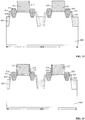
- Figure 17 shows a schematic cross-section view of a corresponding semiconductor structure.
- a first gate oxide layer 470 may be formed on the surface of the first fin structure 410 situated on the bottom of the first opening 600.
- the first gate oxide layer 470 may be used as a component of the subsequently-formed first gate structure in the peripheral region I.
- the first gate oxide layer 470 may be made of SiO x .
- the first gate oxide layer 470 may be formed by an ISSG oxidation process.
- the process parameters used in the ISSG oxidation process may include a process gas including O 2 and H 2 , a flow rate of O 2 in a range of 1 sccm to 30 sccm, a flow rate of H 2 in a range of 1.5 sccm to 15 sccm, and a chamber temperature in a range of 700 °C to 1200 °C.
- the first gate oxide layer 470 may also be simultaneously formed on the surface of the second dummy gate oxide layer 421 on the bottom of the second opening 610.
- the thickness of the first gate oxide layer 470 formed on the surface of the second dummy gate oxide layer 421 on the bottom of the second opening 610 may be smaller than the thickness of the first gate oxide layer 470 formed on the top of first fin structure 411. Further, in a subsequent process, the portion of the first gate oxide layer 470 formed on the surface of the second dummy gate oxide layer 421 on the bottom of the second opening 610 may be removed.
- the second dummy gate oxide layer on the bottom of the second opening may be removed to expose a portion of the surface of the second fin structure (S812).
- Figure 18 shows a schematic cross-section view of a corresponding semiconductor structure.
- the second dummy gate oxide layer 421 on the bottom of the second opening 610 may be removed to expose a portion of the surface of the second fin structure 420.
- the operation power voltage of the devices in the core region II may be smaller than the operation power voltage of the devices in the peripheral region I.
- a larger thickness is required for the dielectric layer when the operation power voltage becomes larger.
- the thickness of the dielectric layer in the core region II may be smaller than the thickness of the dielectric layer in the peripheral region I. Therefore, in one embodiment, before forming the dielectric layer in the core region II, the second dummy gate oxide layer 421 on the bottom of the second opening 610 may be removed.
- the second dummy gate oxide layer 421 on the bottom of the second opening 610 may be removed by a process including the following steps.
- a third patterned layer 530 may be formed to cover the peripheral region I.
- the third patterned layer 530 may expose the surface of the second dummy gate oxide layer 421 (referring to Figure 17 ).
- a dry etching process may then be performed to remove the second dummy gate oxide layer 421 (referring to Figure 17 ) until a portion of the surface of the second fin structure 420 is exposed and the second opening 610.
- the third patterned layer 530 may be removed.
- the portion of the first gate oxide layer 470 formed on the surface of the second dummy gate oxide layer 421 may also be removed during the etching process to remove the second dummy gate oxide layer 421.
- a gate dielectric layer may be formed on the surface of the first gate oxide layer, the sidewall surfaces of the first opening, and the bottom and the sidewall surfaces of the second opening, and then a metal layer may be filled into the first opening and the second opening (S813).
- Figure 19 shows a schematic cross-section view of a corresponding semiconductor structure.
- a gate dielectric layer (not shown) may be formed on the surface of the first gate oxide layer 470, the sidewall surfaces of the first opening 600 (referring to Figure 16 ), and the bottom and the sidewall surfaces of the second opening 610 (referring to Figure 17 ). Then, a metal layer (not shown) may be filled into the first opening 600 and the second opening 610.
- the first gate oxide layer 470 together with the portion of the gate dielectric layer and the metal layer formed in the first opening 600 may form a first gate structure (not shown).
- the portion of the gate dielectric layer and the metal layer formed in the second opening 610 may form a second gate structure (not shown).
- a work function layer (not shown) may be formed on the surface of the gate dielectric layer before further forming the metal layer to fill the first opening 600 and the second opening 610.
- the work function layer when the peripheral region I and the core region II are both N-type regions, the work function layer may be made of an N-type work function material; when the peripheral region I and the core region II are both P-type regions, the work function layer may be made of a P-type work function material.
- the N-type work function material used to form the work function layer may have a work function in a range of 3.9 eV to 4.5 eV.
- the work function of the N-type work function material may be 4.0 eV, 4.1 eV, or 4.3 eV.
- the work function layer may have a single layer structure or a multiple-layer structure.
- the N-type work function material may include one or more of TiAl, TaAlN, TiAIN, MoN, TaCN, AlN, etc. In one embodiment, the work function material used to form the work function layer is TiAl.
- the P-type work function material used to form the work function layer may have a work function in a range of 5.1 eV to 5.5 eV.
- the work function of the P-type work function material may be 5.2 eV, 5.3 eV, or 5.4 eV.
- the work function layer may have a single layer structure or a multiple-layer structure.
- the P-type work function material may include one or more of Ta, TiN, TaN, TaSiN, TiSiN, etc. In one embodiment, the work function material used to form the work function layer is TiN.
- the gate dielectric layer may be made of a high-k dielectric material.
- the high-k dielectric material may refer to a dielectric material with a relative dielectric constant greater than the relative dielectric constant of SiO 2 .
- the high-k dielectric material may include HfO 2 HfSiO, HfSiON, HfTaO, HfTiO, HfZrO, ZrO 2 , Al 2 O 3 , etc.
- the first gate structure and the second gate structure may be formed by a process including the following steps.
- a gate dielectric layer may be formed on the surface of the first gate oxide layer situated on the bottom of the first opening 600, the sidewall surfaces of the first opening 600, and the bottom and sidewall surfaces of the second opening 610.
- the gate dielectric layer may also cover the surface of the dielectric layer 460.
- a work function layer may be formed on the surface of the gate dielectric layer, and then a metal layer may be formed on the surface of the work function layer.
- the metal layer may fill up the first opening 600 and the second opening 610, and the top surface of the metal layer may be higher than the top surface of the dielectric layer 460.
- the portion of the metal layer formed above the top surface of the dielectric layer 460 may then be removed by a planarization process to form a first gate electrode layer 419 on the surface of the work function layer in the peripheral region I and a second gate electrode layer 429 on the surface of the work function layer in the core region II.
- a first gate dielectric layer 417 may be formed on the surface of the first gate oxide layer 470 and the sidewall surfaces of the first opening 600 (referring to Figure 16 ), and a first work function layer 418 may be formed on the surface of the first gate dielectric layer 417; while in the core region, a second gate dielectric layer 427 may be formed on the bottom and the sidewall surfaces of the second opening 610 (referring to Figure 17 ), and a second work function layer 428 may be formed on the surface of the second gate dielectric layer 427.
- the first gate structure may include the first gate oxide layer 470, the first gate dielectric layer 417 formed on the surface of the first gate oxide layer 470 as well as the sidewall surfaces of the first opening 600 (referring to Figure 16 ), the first work function layer 418 formed on the surface of the first gate dielectric layer 417, and the first gate electrode layer 419 formed on the surface of the first work function layer 418;
- the second gate structure may include the second gate dielectric layer 427 formed on the bottom and the sidewall surfaces of the second opening 610 (referring to Figure 17 ), the second work function layer 428 formed on the surface of the second gate dielectric layer 427, and the second gate electrode layer 429 formed on the surface of the second work function layer 428.
- the first gate oxide layer 470 and the first gate dielectric layer 417 may together sever as the gate dielectric layer for the devices in the peripheral region I, and the first work function layer 418 may be used to adjust the threshold voltage of the devices in the peripheral region I.
- the second gate dielectric layer 427 may be used as the gate dielectric layer for the devices in the core region II, and the second work function layer 428 may be used to adjust the threshold voltage of the devices in the core region II.
- the first gate electrode layer 419 may be made of Al, Cu, Ag, Au, Pt, Ni, Ti, or W.
- the second gate electrode layer 429 may also be made of Al, Cu, Ag, Au, Pt, Ni, Ti, or W. In one embodiment, the first gate electrode layer 419 and the second gate electrode layer 429 are both made of W.
- the fabrication process may also include the following steps prior to forming the first gate dielectric layer 417 and the second gate dielectric layer 427.
- an interface layer may be formed on the surface of the first gate oxide layer 470 situated on the bottom of the first opening 600 (referring to Figure 16 ), the sidewall surfaces of the first opening 600, and the bottom and the sidewall surfaces of the second opening 610 (referring to Figure 17 ).
- the interface layer may also cover the surface of the dielectric layer 460.
- the portion of the interface layer formed above the top surface of the dielectric layer 460 may also be removed to form a first interface layer 416 in the peripheral region I on the surface of the first gate oxide layer 470 as well as the sidewall surfaces of the first opening 600, and a second interface layer 426 in the core region II on the bottom and the sidewall surfaces of the second opening 610.
- the damaged first dummy gate oxide layer may be removed and then a first gate oxide layer may be formed on the surface of the first fin structure in the peripheral region. Further, the first gate oxide layer may not experience any etching process, and thus damages to the first gate oxide layer due to etching may be avoided. Therefore the film quality of the first gate oxide layer may be desired. Using such a first gate oxide layer as a part of the dielectric layer of the devices in the peripheral region may improve the quality of the first gate structure in the devices of the peripheral region, and thus the electrical performance of the subsequently-formed semiconductor device may be improved.
- the present invention also provides a semiconductor structure.
- Figure 19 shows a schematic cross-section view of the semiconductor structure.
- the semiconductor structure may include a semiconductor base structure.
- the semiconductor base structure may include a substrate 400 and a plurality of fin structures formed on the substrate 400.
- the substrate may include a peripheral region I and a core region II.
- the plurality of fin structures may be formed in both the core region and the peripheral region.
- the semiconductor structure is described to have a first fin structure 410 formed in the peripheral region I and a second fin structure 420 formed in the core region II.
- the number of the fin structures formed in the peripheral region and the number of the fin structures formed in the core region may be greater than one.
- the semiconductor structure may also include an isolation layer 402 formed on the substrate 400 between neighboring fin structures.
- the isolation layer 402 may cover a portion of the sidewall surfaces of each fin structure and the top surface of the isolation layer 402 may be lower than the top surfaces of the fin structures.
- the semiconductor structure may include a first gate structure (not shown) formed on a portion of the surface of the first fin structure 410.
- the first gate structure may include a first gate oxide layer 470 and a first gate dielectric layer 417 formed on the surface of the first gate oxide layer 470 as well as the sidewall surfaces of a first opening 600 (referring to Figure 16 ), which is formed by removing a first dummy gate structure, initially formed on the surface of the first fin structure 410 in the peripheral region I to occupy a space for the first gate structure.
- the first dummy gate structure may include a first dummy gate oxide layer formed on the surface of the first fin structure and a first dummy gate electrode layer formed on the first dummy gate oxide layer.
- the first gate structure may also include a first work function layer 418 formed on the surface of the first gate dielectric layer 417 and a first gate electrode layer 419 formed on the surface of the first work function layer 418.
- the semiconductor structure may include a second gate structure (not shown) formed on a portion of the surface of the second fin structure 420.
- the second gate structure may include a second gate dielectric layer 427 formed on the bottom and the sidewall surfaces of a second opening 610 (referring to Figure 18 ), which is formed by removing a second dummy gate structure initially formed on the surface of the second fin structure 420 in the core region II to occupy a space for the second gate structure.
- the second dummy gate structure may include a second dummy gate oxide layer formed on the surface of the second fin structure and a second dummy gate electrode layer formed on the second dummy gate oxide layer.
- the second gate structure may also include a second work function layer 428 formed on the surface of the second gate dielectric layer 427 and a second gate electrode layer 429 formed on the surface of the second work function layer 428.
- the first gate oxide layer 470 and the first gate dielectric layer 417 may together sever as the gate dielectric layer for the devices in the peripheral region I, and the first work function layer 418 may be used to adjust the threshold voltage of the devices in the peripheral region I.
- the second gate dielectric layer 427 may be used as the gate dielectric layer for the devices in the core region II, and the second work function layer 428 may be used to adjust the threshold voltage of the devices in the core region II.
- the semiconductor structure may also include a peripheral-region source region (not shown) and a peripheral-region drain region (not shown) formed in a peripheral-region stress layer 414 situated in the first fin structure 410 on the two sides of the first gate structure, and a core-region source region (not shown) and a core-region drain region (not shown) formed in a core-region stress layer 424 situated in the second fin structure 420 on the two sides of the second gate structure.
- the semiconductor structure may also include a sidewall spacer (not shown) formed on each sidewall surface of the first gate structure and the second gate structure, and an etch stop layer 430 formed on the surface of the isolation layer 402, a portion of the top and sidewall surfaces of each fin structure, and the surfaces of the sidewall spacers.
- the semiconductor structure may further include a dielectric layer 460 formed on the etch stop layer 430.
- the top surfaces of the dielectric layer 460, the first gate electrode layer 419, and the second gate electrode layer 429 may be leveled with each other.
- the fabrication process for the semiconductor structure may include the following steps prior to forming the first gate dielectric layer 417 and the second gate dielectric layer 427.
- an interface layer may be formed on the surface of the first gate oxide layer 470 situated on the bottom of the first opening 600 (referring to Figure 16 ), the sidewall surfaces of the first opening 600, and the bottom and the sidewall surfaces of the second opening 610 (referring to Figure 18 ).
- the interface layer may also cover the surface of the dielectric layer 460.
- the portion of the interface layer formed above the top surface of the dielectric layer 460 may also be removed to form a first interface layer 416 in the peripheral region I on the surface of the first gate oxide layer 470 as well as the sidewall surfaces of the first opening 600, and a second interface layer 426 in the core region II on the bottom and the sidewall surfaces of the second opening 610.
- the damaged first dummy gate oxide layer may be removed and then a first gate oxide layer may be formed on the surface of the first fin structure in the peripheral region. Further, the first gate oxide layer may not experience any etching process, and thus damages to the first gate oxide layer due to etching may be avoided. Therefore the film quality of the first gate oxide layer may be desired. Using such a first gate oxide layer as a part of the dielectric layer of the devices in the peripheral region may improve the quality of the first gate structure in the devices of the peripheral region, and thus the electrical performance of the subsequently-formed semiconductor device may be improved.
- the disclosed semiconductor structures and fabrication methods may demonstrates several advantages.
- a first dummy gate structure is formed on the surface of a first fin structure in a peripheral region, while a second dummy gate structure is formed on the surface of a second fin structure in a core region.
- the first dummy gate structure includes a first dummy gate oxide layer formed on the surface of the first fin structure and a first dummy gate electrode layer formed on the surface of the first dummy gate oxide layer
- the second dummy gate structure includes a second dummy gate oxide layer formed on the surface of the second fin structure and a second dummy gate electrode layer formed on the surface of the second dummy gate oxide layer.
- the first dummy gate electrode layer and the second dummy gate electrode layer may be removed to expose the first dummy gate oxide layer and the second dummy gate oxide layer. Further, the first dummy gate oxide layer is removed to expose the surface of a portion of the fist fin structure. A first gate oxide layer may then be formed on the exposed surface of the first fin structure. After forming the first oxide layer, the second dummy gate oxide layer may then be removed. Finally, by further forming a gate dielectric layer and a gate electrode layer, a first fin structure may be formed on the surface of the first fin structure in the peripheral region while a second fin structure may be formed on the surface of the second fin structure in the core region.
- a first dummy gate structure is formed to occupy a space for a subsequently-formed first gate structure
- a second dummy gate structure is formed to occupy a space for a subsequently-formed second gate structure.
- a first gate oxide layer may be formed on the surface of the first fin structure. That is, a gate oxide layer may be re-formed on the first fin structure after removing the first dummy gate structure. Because the re-formed first gate oxide layer may not experience any etching process, damages to the first gate oxide layer due to etching may be avoided. Therefore, the film quality of the first gate oxide layer may be desired. Using such a first gate oxide layer as a part of the dielectric layer of the devices in the peripheral region may improve the quality of the first gate structure in the devices of the peripheral region, and thus the electrical performance of the subsequently-formed semiconductor device may be improved.
Landscapes
- Metal-Oxide And Bipolar Metal-Oxide Semiconductor Integrated Circuits (AREA)
- Electrodes Of Semiconductors (AREA)
- Physics & Mathematics (AREA)
- Engineering & Computer Science (AREA)
- Plasma & Fusion (AREA)
- Insulated Gate Type Field-Effect Transistor (AREA)
Applications Claiming Priority (1)
| Application Number | Priority Date | Filing Date | Title |
|---|---|---|---|
| CN201510746439.3A CN106684144B (zh) | 2015-11-05 | 2015-11-05 | 半导体结构的制造方法 |
Publications (1)
| Publication Number | Publication Date |
|---|---|
| EP3166136A1 true EP3166136A1 (fr) | 2017-05-10 |
Family
ID=57209302
Family Applications (1)
| Application Number | Title | Priority Date | Filing Date |
|---|---|---|---|
| EP16196137.0A Withdrawn EP3166136A1 (fr) | 2015-11-05 | 2016-10-27 | Structures à semi-conducteurs et leurs procédé de fabrication |
Country Status (3)
| Country | Link |
|---|---|
| US (1) | US9911833B2 (fr) |
| EP (1) | EP3166136A1 (fr) |
| CN (1) | CN106684144B (fr) |
Cited By (2)
| Publication number | Priority date | Publication date | Assignee | Title |
|---|---|---|---|---|
| CN114512542A (zh) * | 2022-01-27 | 2022-05-17 | 上海华力集成电路制造有限公司 | 一种改善io栅氧损伤的方法 |
| US20230335601A1 (en) * | 2019-04-30 | 2023-10-19 | Taiwan Semiconductor Manufacturing Co., Ltd. | Selective Etching to Increase Threshold Voltage Spread |
Families Citing this family (21)
| Publication number | Priority date | Publication date | Assignee | Title |
|---|---|---|---|---|
| US10050147B2 (en) * | 2015-07-24 | 2018-08-14 | Taiwan Semiconductor Manufacturing Co., Ltd. | Semiconductor device and manufacturing method thereof |
| US9601567B1 (en) | 2015-10-30 | 2017-03-21 | Taiwan Semiconductor Manufacturing Co., Ltd. | Multiple Fin FET structures having an insulating separation plug |
| US10020304B2 (en) * | 2015-11-16 | 2018-07-10 | Taiwan Semiconductor Manufacturing Co., Ltd. | Fin field effect transistor, semiconductor device and fabricating method thereof |
| CN106024893B (zh) * | 2016-05-30 | 2019-03-19 | 上海华力微电子有限公司 | 高k金属栅器件及其制备方法 |
| US10490649B2 (en) * | 2017-05-30 | 2019-11-26 | Taiwan Semiconductor Manufacturing Company, Ltd. | Method of fabricating semiconductor device with adhesion layer |
| CN109087863B (zh) * | 2017-06-14 | 2022-02-15 | 中芯国际集成电路制造(北京)有限公司 | 半导体结构及其形成方法 |
| US10236220B1 (en) * | 2017-08-31 | 2019-03-19 | Taiwan Semiconductor Manufacturing Company, Ltd. | Fin field-effect transistor device and method |
| CN109494190B (zh) * | 2017-09-11 | 2020-07-10 | 中芯国际集成电路制造(上海)有限公司 | 一种鳍式场效应半导体的形成方法 |
| US10679988B2 (en) * | 2017-09-18 | 2020-06-09 | Taiwan Semiconductor Manufacturing Co., Ltd. | Semiconductor device including FinFETS having different channel heights and manufacturing method thereof |
| CN110517989A (zh) * | 2018-05-21 | 2019-11-29 | 中芯国际集成电路制造(上海)有限公司 | 半导体结构及其形成方法 |
| CN110690109B (zh) * | 2018-07-05 | 2021-10-15 | 中芯国际集成电路制造(上海)有限公司 | 半导体器件及其形成方法 |
| US10867860B2 (en) | 2018-08-30 | 2020-12-15 | Taiwan Semiconductor Manufacturing Company, Ltd. | Methods of forming FinFET device |
| US11011625B2 (en) * | 2018-09-20 | 2021-05-18 | Taiwan Semiconductor Manufacturing Co., Ltd. | Liner for a bi-layer gate helmet and the fabrication thereof |
| US10867864B2 (en) * | 2018-09-27 | 2020-12-15 | Taiwan Semiconductor Manufacturing Company, Ltd. | Semiconductor device and method of manufacture |
| US11217484B2 (en) * | 2018-10-31 | 2022-01-04 | Taiwan Semiconductor Manufacturing Co., Ltd. | FinFET gate structure and related methods |
| CN111863609B (zh) * | 2019-04-30 | 2023-03-10 | 中芯国际集成电路制造(上海)有限公司 | 半导体结构及其形成方法 |
| US11211472B2 (en) * | 2020-02-24 | 2021-12-28 | Taiwan Semiconductor Manufacturing Co., Ltd. | Semiconductor device and method of forming the same |
| CN113540236B (zh) * | 2020-04-13 | 2024-11-22 | 中芯国际集成电路制造(上海)有限公司 | 半导体结构及其形成方法 |
| CN113539826B (zh) * | 2020-04-17 | 2025-02-25 | 中芯国际集成电路制造(上海)有限公司 | 半导体结构及其形成方法 |
| CN113871352B (zh) * | 2020-06-30 | 2024-03-08 | 中芯国际集成电路制造(上海)有限公司 | 半导体结构的制作方法 |
| CN114300360B (zh) * | 2021-11-29 | 2025-03-14 | 上海华力集成电路制造有限公司 | 一种先切SDB FinFET的制造方法 |
Citations (3)
| Publication number | Priority date | Publication date | Assignee | Title |
|---|---|---|---|---|
| JP2008016522A (ja) * | 2006-07-04 | 2008-01-24 | Sony Corp | 半導体装置の製造方法および半導体装置 |
| US20140319623A1 (en) * | 2011-12-28 | 2014-10-30 | Curtis Tsai | Methods of integrating multiple gate dielectric transistors on a tri-gate (finfet) process |
| US20140339645A1 (en) * | 2013-05-14 | 2014-11-20 | Global Foundries Inc. | Methods of forming semiconductor devices with different insulation thicknesses on the same semiconductor substrate and the resulting devices |
Family Cites Families (4)
| Publication number | Priority date | Publication date | Assignee | Title |
|---|---|---|---|---|
| US8803253B2 (en) * | 2012-09-11 | 2014-08-12 | Texas Instruments Incorporated | Replacement metal gate process for CMOS integrated circuits |
| KR102066848B1 (ko) * | 2013-06-24 | 2020-01-16 | 삼성전자 주식회사 | 반도체 소자 및 그 제조 방법 |
| US20150021681A1 (en) * | 2013-07-16 | 2015-01-22 | United Microelectronics Corp. | Semiconductor device having metal gate and manufacturing method thereof |
| CN105336688B (zh) * | 2014-05-28 | 2018-07-10 | 中芯国际集成电路制造(上海)有限公司 | 半导体结构的形成方法 |
-
2015
- 2015-11-05 CN CN201510746439.3A patent/CN106684144B/zh active Active
-
2016
- 2016-10-26 US US15/335,248 patent/US9911833B2/en active Active
- 2016-10-27 EP EP16196137.0A patent/EP3166136A1/fr not_active Withdrawn
Patent Citations (3)
| Publication number | Priority date | Publication date | Assignee | Title |
|---|---|---|---|---|
| JP2008016522A (ja) * | 2006-07-04 | 2008-01-24 | Sony Corp | 半導体装置の製造方法および半導体装置 |
| US20140319623A1 (en) * | 2011-12-28 | 2014-10-30 | Curtis Tsai | Methods of integrating multiple gate dielectric transistors on a tri-gate (finfet) process |
| US20140339645A1 (en) * | 2013-05-14 | 2014-11-20 | Global Foundries Inc. | Methods of forming semiconductor devices with different insulation thicknesses on the same semiconductor substrate and the resulting devices |
Cited By (3)
| Publication number | Priority date | Publication date | Assignee | Title |
|---|---|---|---|---|
| US20230335601A1 (en) * | 2019-04-30 | 2023-10-19 | Taiwan Semiconductor Manufacturing Co., Ltd. | Selective Etching to Increase Threshold Voltage Spread |
| US12513961B2 (en) * | 2019-04-30 | 2025-12-30 | Taiwan Semiconductor Manufacturing Company, Ltd. | Selective etching to increase threshold voltage spread |
| CN114512542A (zh) * | 2022-01-27 | 2022-05-17 | 上海华力集成电路制造有限公司 | 一种改善io栅氧损伤的方法 |
Also Published As
| Publication number | Publication date |
|---|---|
| US20170133489A1 (en) | 2017-05-11 |
| CN106684144A (zh) | 2017-05-17 |
| CN106684144B (zh) | 2019-11-01 |
| US9911833B2 (en) | 2018-03-06 |
Similar Documents
| Publication | Publication Date | Title |
|---|---|---|
| US9911833B2 (en) | Semiconductor structures and fabrication methods thereof | |
| US10685889B2 (en) | Semiconductor structures and fabrication methods thereof | |
| US11735650B2 (en) | Structure and method for FinFET device with buried sige oxide | |
| US11018246B2 (en) | Integrated circuit with a fin and gate structure and method making the same | |
| US10269927B2 (en) | Semiconductor structures and fabrication methods thereof | |
| US11011641B2 (en) | Flat STI surface for gate oxide uniformity in Fin FET devices | |
| US11063119B2 (en) | Semiconductor structure and method for forming the same | |
| US9368497B2 (en) | Fin field-effect transistors and fabrication method thereof | |
| US9349866B2 (en) | Structure and method for FinFET device | |
| EP3306665A2 (fr) | Structure à semi-conducteurs et son procédé de fabrication | |
| TWI567981B (zh) | 鰭部件的結構及其製造方法 | |
| CN106504990A (zh) | 半导体装置以及制造鳍式场效晶体管装置的方法 | |
| CN105280706B (zh) | 具有栅极氧化物层的finfet器件 | |
| CN106952908B (zh) | 半导体结构及其制造方法 | |
| US12317527B2 (en) | Integrated circuit with a Fin and gate structure and method making the same | |
| CN108538724B (zh) | 半导体结构及其形成方法 | |
| CN103811538B (zh) | 具有器件收益和生产率改进的金属栅极结构 | |
| CN107481933A (zh) | 半导体结构及其制造方法 | |
| CN108389905B (zh) | 半导体结构及其形成方法 | |
| CN106876335B (zh) | 半导体结构的制造方法 | |
| CN109003976B (zh) | 半导体结构及其形成方法 | |
| CN110875390B (zh) | 半导体结构及其形成方法 | |
| CN113327857B (zh) | 半导体结构及其形成方法 | |
| CN118198001A (zh) | 半导体结构的形成方法 |
Legal Events
| Date | Code | Title | Description |
|---|---|---|---|
| PUAI | Public reference made under article 153(3) epc to a published international application that has entered the european phase |
Free format text: ORIGINAL CODE: 0009012 |
|
| STAA | Information on the status of an ep patent application or granted ep patent |
Free format text: STATUS: THE APPLICATION HAS BEEN PUBLISHED |
|
| AK | Designated contracting states |
Kind code of ref document: A1 Designated state(s): AL AT BE BG CH CY CZ DE DK EE ES FI FR GB GR HR HU IE IS IT LI LT LU LV MC MK MT NL NO PL PT RO RS SE SI SK SM TR |
|
| AX | Request for extension of the european patent |
Extension state: BA ME |
|
| RAP1 | Party data changed (applicant data changed or rights of an application transferred) |
Owner name: SEMICONDUCTOR MANUFACTURING INTERNATIONAL CORPORAT |
|
| STAA | Information on the status of an ep patent application or granted ep patent |
Free format text: STATUS: REQUEST FOR EXAMINATION WAS MADE |
|
| 17P | Request for examination filed |
Effective date: 20170718 |
|
| RBV | Designated contracting states (corrected) |
Designated state(s): AL AT BE BG CH CY CZ DE DK EE ES FI FR GB GR HR HU IE IS IT LI LT LU LV MC MK MT NL NO PL PT RO RS SE SI SK SM TR |
|
| RAP1 | Party data changed (applicant data changed or rights of an application transferred) |
Owner name: SEMICONDUCTOR MANUFACTURING INTERNATIONAL (BEIJING Owner name: SEMICONDUCTOR MANUFACTURING INTERNATIONAL (SHANGHA |
|
| STAA | Information on the status of an ep patent application or granted ep patent |
Free format text: STATUS: EXAMINATION IS IN PROGRESS |
|
| 17Q | First examination report despatched |
Effective date: 20200330 |
|
| STAA | Information on the status of an ep patent application or granted ep patent |
Free format text: STATUS: THE APPLICATION IS DEEMED TO BE WITHDRAWN |
|
| 18D | Application deemed to be withdrawn |
Effective date: 20200811 |